

Page 1

www.ti.com
查询ONET4291PA供应商
1-Gbps to 4.25-Gbps Rate-Selectable Limiting Amplifier
ONET4291PA
SLLS671 – SEPTEMBER 2005
FEATURES
• CML Data Outputs With On-Chip, 50- Ω
Back-Termination to V
CC• Multirate Operation from 1 Gbps up to
4.25 Gbps • Single 3.3-V Supply
• Loss-of-Signal Detection (LOS) • Surface-Mount, Small-Footprint, 4-mm ×
• Two-Wire Digital Interface
• Digitally Selectable LOS Threshold
• Digitally Selectable Bandwidth
• Digitally Selectable Output Voltage
• Low Power Consumption
• Input Offset Cancellation
4-mm, 16-Terminal QFN Package
APPLICATIONS
• Multirate SONET/SDH Transmission Systems
• 4.25-Gbps, 2.125-Gbps, and 1.0625-Gbps
Fibre-Channel Receivers
• Gigabit Ethernet Receivers
DESCRIPTION
The ONET4291PA is a versatile, high-speed, rate-selectable limiting amplifier for multiple fiber-optic applications
with data rates up to 4.25 Gbps.
The device provides a two-wire interface, which allows digital bandwidth selection, digital output amplitude
selection, and digital loss of signal threshold adjust.
This device provides a gain of about 43 dB, which ensures a fully differential output swing for input signals as low
as 5 mV
The ONET4291PA provides loss-of-signal detection with either digital or analog threshold adjust.
The part is available in a small-footprint, 4-mm × 4-mm, 16-terminal QFN package. It requires a single 3.3-V
supply.
This power-efficient, rate-selectable limiting amplifier is characterized for operation from –40 ° C to 85 ° C ambient
temperature.
.
p-p
Please be aware that an important notice concerning availability, standard warranty, and use in critical applications of Texas
Instruments semiconductor products and disclaimers thereto appears at the end of this data sheet.
PRODUCTION DATA information is current as of publication date.
Products conform to specifications per the terms of the Texas
Instruments standard warranty. Production processing does not
necessarily include testing of all parameters.
Copyright © 2005, Texas Instruments Incorporated
Page 2
www.ti.com
DIN+
DIN−
Band-Gap Voltage
Reference and
Bias Current Generation
Bandwidth
Switch
COC+
COC−
50 Ω
Gain Stage
DC Feedback Stage
CML Output Buffer
Peak
Detector
Loss-of-Signal Detection
Two-Wire
Interface
and
Control
Logic
Programmable
Resistor
V
CC
GND
SDA
SCK
DOUT+
DOUT−
LOS
SD
RTHI
6
50 Ω
+
−
+
−
4
2
TH
+
−
Peak
Detector
Gain Stage
+
−
2
B0067-01
ONET4291PA
SLLS671 – SEPTEMBER 2005
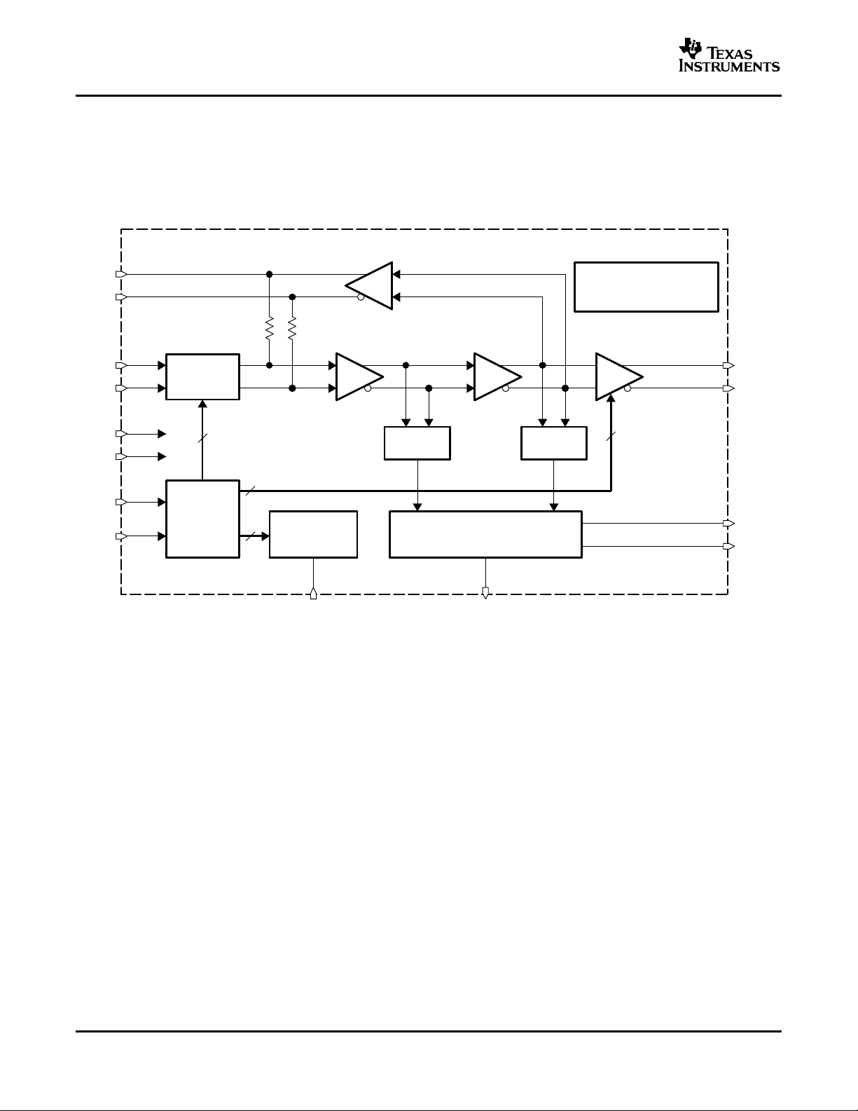
BLOCK DIAGRAM
A simplified block diagram of the ONET4291PA is shown in Figure 1 .
This compact, 3.3-V, low-power, 1-Gbps to 4.25-Gbps rate-selectable limiting amplifier consists of a high-speed
data path with offset cancellation block (dc feedback), a loss-of-signal detection block using two peak detectors,
a programmable resistor, a two-wire interface and control-logic block, and a band-gap voltage reference and
bias-current generation block.
Figure 1. Simplified Block Diagram of the ONET4291PA
HIGH-SPEED DATA PATH
The high-speed data signal is applied to the data path by means of the input signal terminals DIN+ and DIN–.
The data path consists of a digitally controllable bandwidth switch followed by two 50- Ω on-chip line termination
resistors; two gain stages, which provide a typical gain of about 37 dB; and a CML output stage, which provides
another 6-dB gain. The amplified data-output signal is available at the output terminals DOUT+ and DOUT–,
which feature on-chip 2 × 50- Ω back-termination to V
A dc feedback stage compensates for internal offset voltages and thus ensures proper operation even for small
input data signals. This stage is driven by the output signal of the second gain stage. The signal is low-pass
filtered, amplified, and fed back to the input of the first gain stage via the on-chip 50- Ω termination resistors. The
required low-frequency cutoff is determined by an external 0.1- µ F capacitor, which must be differentially
connected to the COC+ and COC– terminals.
LOSS-OF-SIGNAL DETECTION AND PROGRAMMABLE RESISTOR
The peak values of the output signals of the first and second gain stages are monitored by two peak detectors.
The peak values are compared to a predefined loss-of-signal threshold voltage inside the loss-of-signal detection
block. As a result of the comparison, the loss-of-signal detection block generates the SD signal, which indicates a
sufficient input-signal amplitude, or the LOS signal, which indicates that the input signal amplitude is below the
defined threshold level.
2
.
CC
Page 3
www.ti.com
R6
40 kΩ
RTHI
R7
8 kΩ
LOS Threshold Register
R5
20 kΩ
R4
10 kΩ
R3
5 kΩ
R2
2.5 kΩ
R1
1.25 kΩ
From 2-Wire Interface and Control Logic Block
S0098-01
ONET4291PA
SLLS671 – SEPTEMBER 2005
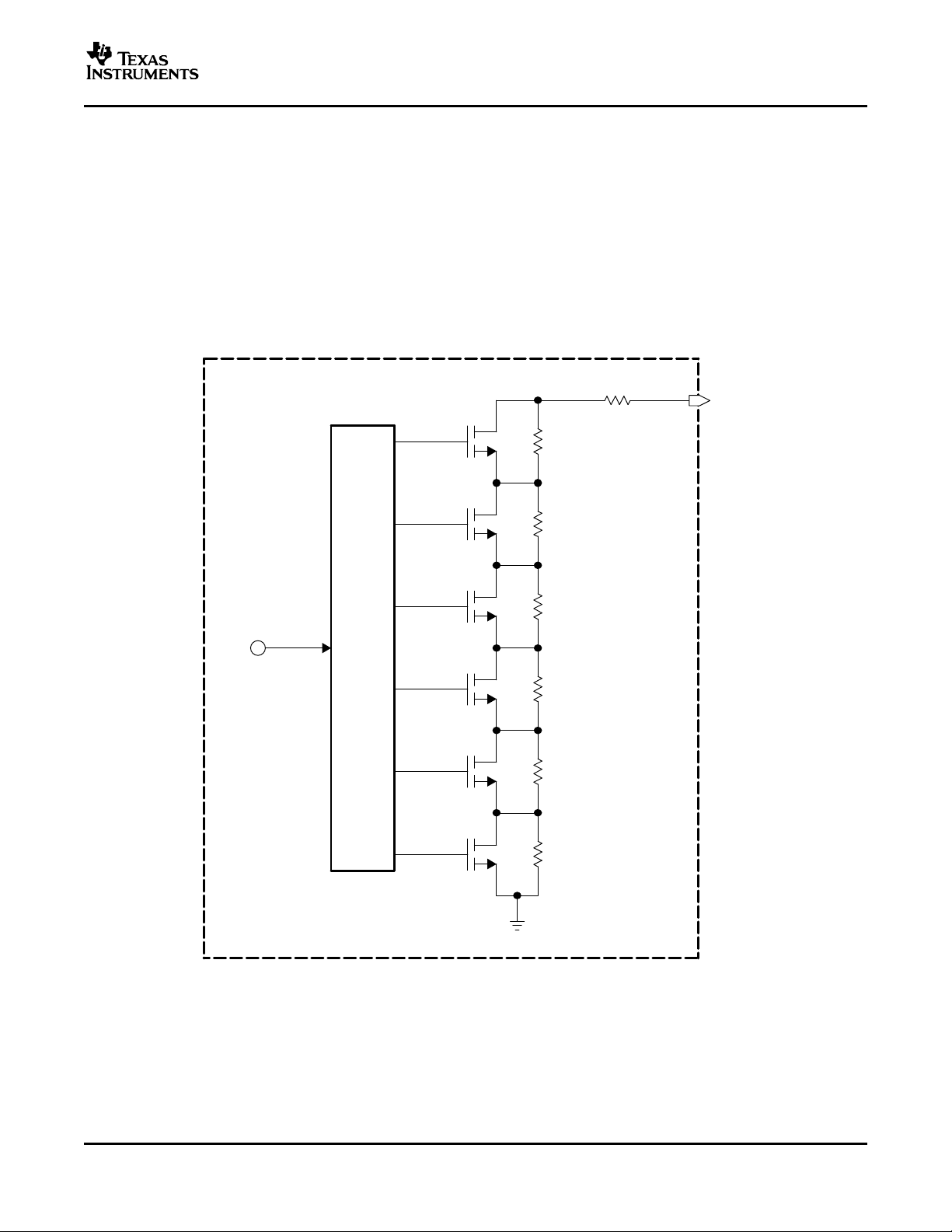
The threshold voltage can be set within a certain range by means of an external resistor connected between the
TH terminal and ground (GND). Alternatively, shorting the TH and RTHI terminals causes an internal, digitally
selectable resistor to be used for threshold adjustment. The resistor value is selectable using the two-wire
interface.
The principle of the digitally selectable resistor is shown in Figure 2 . The complete resistor between the RTHI
terminal and GND consists of seven series-connected resistors.
Six of the resistors have binary-weighted resistance values, and each can be shunted individually by means of a
parallel-connected MOS transistor.
The seventh resistor defines the minimum remaining resistance in case all six MOS devices are conductive.
With the resistor values shown in Figure 2 , the minimum selectable resistance is 8 k Ω , the maximum resistance
is 86.75 k Ω , and the resolution is 1.25 k Ω /step.
Figure 2. Digitally Controllable On-Chip Resistor
3
Page 4
www.ti.com
Start/Stop
Detector
Logic
111
110
101
100
011
010
001
000
START
STOP
SDA
SCK
8-Bit Register
Bandwidth (4 Bits)
Unused (4 Bits)
8
8
8-Bit Register
LOS Threshold (6 Bits)
Output Amplitude (2 Bits)
8
11-Bit Shift Register
8 Bits Data 3 Bits Addr
3-to-8 Decoder
3
B0068-01
ONET4291PA
SLLS671 – SEPTEMBER 2005
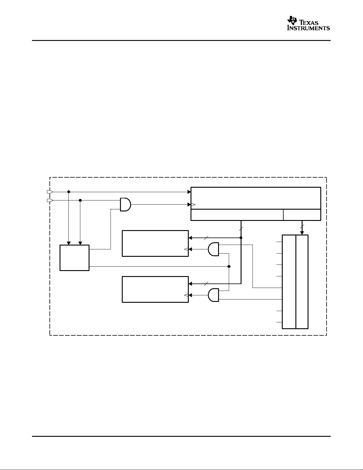
TWO-WIRE INTERFACE AND CONTROL LOGIC
The ONET4291PA uses a two-wire serial interface for digital control of the amplifier bandwidth, output amplitude,
and LOS threshold. A simplified block diagram of this interface is given in Figure 3 .
SDA and SCK are inputs for the serial data and the serial clock, respectively, and can be driven by a
microprocessor. Both inputs have 100-k Ω pullup resistors to V
is recommended.
A write cycle consists of a START command, 3 address bits with MSB first, 8 data bits with MSB first, and a
STOP command. In idle mode, both the SDA and SCK lines are at a high level.
A START command is initiated by a falling edge on SDA with SCK at a high level.
Bits are clocked into an 11-bit-wide shift register while the SCK level is high.
A STOP command is detected on the rising edge of SDA after SCK has changed from a low level to a high level.
At the time of detection of a STOP command, the 8 data bits from the shift register are copied to a selected 8-bit
register. Register selection occurs according to the 3 address bits in the shift register, which are decoded to 8
independent select signals using a 3-to-8 decoder block.
In the ONET4291PA, only addresses 4 (100b) and 5 (101b) are used.
. For driving these inputs, an open-drain output
CC
4
Figure 3. Simplified Two-Wire Interface Block Diagram
Page 5
www.ti.com
START STOP1 0 1 0 1 1
SDA
SCK
DTA
R
DTA
F
STRT
HLD
CLK
R
CLK
F
CLK
HI
DTA
HI
DTA
STP
DTA
WT
DTA
HLD
STOP
STP
T0077-01
ONET4291PA
SLLS671 – SEPTEMBER 2005
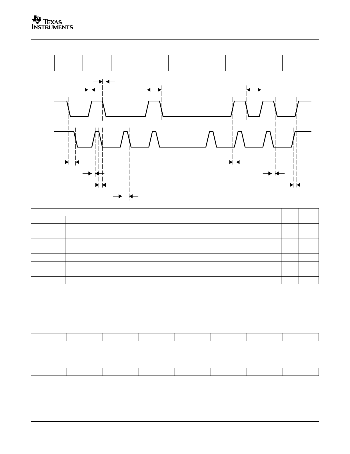
The timing definition for the serial data signal SDA and the serial clock signal SCK is shown in Figure 4 .
PARAMETER DESCRIPTION MIN MAX UNIT
STRT
HLD
CLK
, DTA
R
CLK
, DTA
F
CLK
HI
DTA
HI
DTA
STP
DTA
WT
DTA
HLD
STOP
STP
START hold time Time required from data falling edge to clock falling edge at START 10 ns
Clock and data rise time Clock and data rise time 10 ns
R
Clock and data fall time Clock and data fall time 10 ns
F
Clock high time Minimum clock high period 50 ns
Data high time Minimum data high period 100 ns
Data setup time Minimum time from data rising edge to clock rising edge 10 ns
Data wait time Minimum time from data falling edge to data rising edge 50 ns
Data hold time Minimum time from clock falling edge to data falling edge 10 ns
STOP setup time Minimum time from clock rising edge to data rising edge at STOP 10 ns
Figure 4. Two-Wire Interface Timing Diagram
The register mapping for register addresses 4 (100b) and 5 (101b) is shown in Table 1 and Table 2 , respectively.
Table 1. Register 4 (100b) Mapping
BIT 7 BIT 6 BIT 5 BIT 4 BIT 3 BIT 2 BIT 1 BIT 0
BW3 BW2 BW1 BW0 – – – –
Table 2. Register 5 (101b) Mapping
BIT 7 BIT 6 BIT 5 BIT 4 BIT 3 BIT 2 BIT 1 BIT 0
A1 A0 R5 R4 R3 R2 R1 R0
Table 3 through Table 5 describe circuit functionality based on the register settings.
5
Page 6
www.ti.com
ONET4291PA
SLLS671 – SEPTEMBER 2005
BW3 BW2 BW1 BW0 TYP UNIT
0 0 0 0 4.39 GHz
0 0 0 1 3.91 GHz
0 0 1 0 3.47 GHz
0 0 1 1 3.03 GHz
0 1 0 0 2.81 GHz
0 1 0 1 2.31 GHz
0 1 1 0 1.82 GHz
0 1 1 1 1.60 GHz
1 0 0 0 1.55 GHz
1 0 0 1 1.33 GHz
1 0 1 0 1.11 GHz
1 0 1 1 1.03 GHz
1 1 0 0 0.86 GHz
1 1 0 1 0.82 GHz
1 1 1 0 0.76 GHz
1 1 1 1 0.73 GHz
Table 3. Bandwidth Selection
Table 4. Output Amplitude Selection
A1 A0 TYP UNIT
0 0 400 mV
0 1 600 mV
1 0 800 mV
1 1 1000 mV
p-p
p-p
p-p
p-p
Table 5. LOS-Threshold Digitally Controlled Resistor Selection
R5 R4 R3 R2 R1 R0 TYP UNIT
0 0 0 0 0 0 86.75 k Ω
0 0 0 0 0 1 85.5 k Ω
0 0 0 0 1 0 84.25 k Ω
0 0 0 0 1 1 83 k Ω
0 0 0 1 0 0 81.75 k Ω
0 0 0 1 0 1 80.5 k Ω
0 0 0 1 1 0 79.25 k Ω
0 0 0 1 1 1 78 k Ω
0 0 1 0 0 0 76.75 k Ω
0 0 1 0 0 1 75.5 k Ω
0 0 1 0 1 0 74.25 k Ω
0 0 1 0 1 1 73 k Ω
0 0 1 1 0 0 71.75 k Ω
0 0 1 1 0 1 70.5 k Ω
0 0 1 1 1 0 69.25 k Ω
0 0 1 1 1 1 68 k Ω
0 1 0 0 0 0 66.75 k Ω
0 1 0 0 0 1 65.5 k Ω
0 1 0 0 1 0 64.25 k Ω
0 1 0 0 1 1 63 k Ω
0 1 0 1 0 0 61.75 k Ω
6
Page 7

www.ti.com
ONET4291PA
SLLS671 – SEPTEMBER 2005
Table 5. LOS-Threshold Digitally Controlled Resistor Selection (continued)
R5 R4 R3 R2 R1 R0 TYP UNIT
0 1 0 1 0 1 60.5 k Ω
0 1 0 1 1 0 59.25 k Ω
0 1 0 1 1 1 58 k Ω
0 1 1 0 0 0 56.75 k Ω
0 1 1 0 0 1 55.5 k Ω
0 1 1 0 1 0 54.25 k Ω
0 1 1 0 1 1 53 k Ω
0 1 1 1 0 0 51.75 k Ω
0 1 1 1 0 1 50.5 k Ω
0 1 1 1 1 0 49.25 k Ω
0 1 1 1 1 1 48 k Ω
1 0 0 0 0 0 46.75 k Ω
1 0 0 0 0 1 45.5 k Ω
1 0 0 0 1 0 44.25 k Ω
1 0 0 0 1 1 43 k Ω
1 0 0 1 0 0 41.75 k Ω
1 0 0 1 0 1 40.5 k Ω
1 0 0 1 1 0 39.25 k Ω
1 0 0 1 1 1 38 k Ω
1 0 1 0 0 0 36.75 k Ω
1 0 1 0 0 1 35.5 k Ω
1 0 1 0 1 0 34.25 k Ω
1 0 1 0 1 1 33 k Ω
1 0 1 1 0 0 31.75 k Ω
1 0 1 1 0 1 30.5 k Ω
1 0 1 1 1 0 29.25 k Ω
1 0 1 1 1 1 28 k Ω
1 1 0 0 0 0 26.75 k Ω
1 1 0 0 0 1 25.5 k Ω
1 1 0 0 1 0 24.25 k Ω
1 1 0 0 1 1 23 k Ω
1 1 0 1 0 0 21.75 k Ω
1 1 0 1 0 1 20.5 k Ω
1 1 0 1 1 0 19.25 k Ω
1 1 0 1 1 1 18 k Ω
1 1 1 0 0 0 16.75 k Ω
1 1 1 0 0 1 15.5 k Ω
1 1 1 0 1 0 14.25 k Ω
1 1 1 0 1 1 13 k Ω
1 1 1 1 0 0 11.75 k Ω
1 1 1 1 0 1 10.5 k Ω
1 1 1 1 1 0 9.25 k Ω
1 1 1 1 1 1 8 k Ω
7
Page 8

www.ti.com
GND
DOUT+
DOUT−
GND
1
2
3
4
LOS
SD
SCK
SDA
RGV PACKAGE
(TOP VIEW)
12
11
10
9
16
V
CC
V
CC
TH
RTHI
15 14 13
5 6 7 8
COC−
COC+
DIN+
DIN−
P0030-01
ONET4291PA
SLLS671 – SEPTEMBER 2005
BAND-GAP VOLTAGE AND BIAS GENERATION
The ONET4291PA limiting amplifier is supplied by a single, 3.3-V supply voltage connected to the V
This voltage is referred to GND.
On-chip band-gap voltage circuitry generates a reference voltage, independent of supply voltage, from which all
other internally required voltages and bias currents are derived.
TERMINAL ASSIGNMENTS
For the ONET4291PA, a small-footprint 4-mm × 4-mm, 16-terminal QFN package is used, with a terminal pitch of
0,65 mm.
terminals.
CC
TERMINAL DESCRIPTION
TERMINAL
NAME NO.
COC+ 6 Analog
COC– 5 Analog
DIN+ 7 Analog input
DIN– 8 Analog input
DOUT+ 15 CML output Non-inverted data output. On-chip 50- Ω back-terminated to VCC.
DOUT– 14 CML output Inverted data output. On-chip 50- Ω back-terminated to VCC.
GND 13, 16, EP Supply Circuit ground. Exposed die pad (EP) must be grounded.
LOS 1
RTHI 9 Analog
SCK 3 CMOS input Two-wire interface serial clock. Includes a 100-k Ω pullup resistor to VCC.
SD 2 CMOS output
SDA 4 CMOS input Two-wire interface serial data input. Includes a 100-k Ω pullup resistor to VCC.
TH 10 Analog input
V
CC
8
11, 12 Supply 3.3-V, +10%/–12% supply voltage
TYPE DESCRIPTION
Offset cancellation filter capacitor plus terminal. An external 0.1- µ F filter capacitor must be
connected between this terminal and COC– (terminal 5).
Offset cancellation filter capacitor minus terminal. An external 0.1- µ F filter capacitor must be
connected between this terminal and COC+ (terminal 6).
Non-inverted data input. On-chip 50- Ω terminated to COC+. Differentially 100- Ω terminated
to DIN–.
Inverted data input. On-chip 50- Ω terminated to COC–. Differentially 100- Ω terminated to
DIN+.
Open-drain High level indicates that the input signal amplitude is below the programmed threshold level.
MOS Open-drain output. Requires an external 10-k Ω pullup resistor to V
Digitally controlled internal resistor to ground, which can be used for LOS threshold
adjustment. A 6-bit-wide control register can be set via the two-wire interface.
High level indicates that sufficient input signal amplitude is applied to the device. Low level
indicates that the input signal amplitude is below the programmed threshold level.
LOS threshold adjustment with resistor to GND. For use of the internal digitally controlled
resistor, connect TH with RTHI (terminal 9).
for proper operation.
CC
Page 9

www.ti.com
ONET4291PA
SLLS671 – SEPTEMBER 2005
ABSOLUTE MAXIMUM RATINGS
over operating free-air temperature range (unless otherwise noted)
V
V
V
V
VTH, V
V
I
LOS
I
DIN+
I
DOUT–
CC
, V
DIN+
DIN–
, VSD, V
LOS
, V
COC+
DOUT+
DIN,DIFF
, I
DIN–
COC–
, V
SCK
, V
RTHI
, V
DOUT–
, I
, Continuous current at inputs and outputs 20 mA
DOUT+
Supply voltage
Voltage at DIN+, DIN–
, Voltage at LOS, SD, SCK, SDA, COC+, COC–, RTHI, TH, DOUT+, DOUT–
SDA
,
Differential voltage between DIN+ and DIN– ± 1.25 V
Current into LOS 10 mA
ESD ESD rating at all terminals (HBM) 4 kV
T
J,max
T
stg
T
A
T
LEAD
Maximum junction temperature 125 ° C
Storage temperature range –65 ° C to 85 ° C
Characterized free-air operating temperature range –40 ° C to 85 ° C
Lead temperature 1,6 mm (1/16 inch) from case for 10 seconds 260 ° C
(1) Stresses beyond those listed under "absolute maximum ratings" may cause permanent damage to the device. These are stress ratings
only, and functional operation of the device at these or any other conditions beyond those indicated under "recommended operating
conditions" is not implied. Exposure to absolute-maximum-rated conditions for extended periods may affect device reliability.
(2) All voltage values are with respect to network ground terminal.
(2)
(2)
(1)
–0.3 V to 4 V
0.5 V to 4 V
(2)
–0.3 V to 4 V
RECOMMENDED OPERATING CONDITIONS
over operating free-air temperature range (unless otherwise noted)
MIN NOM MAX UNIT
VCC, V
T
A
Supply voltage 2.9 3.3 3.6 V
CCO
Operating free-air temperature –40 85 ° C
CMOS input high voltage 2 V
CMOS input low voltage 0.8 V
DC ELECTRICAL CHARACTERISTICS
over recommended operating conditions (unless otherwise noted). Typical values are at V
PARAMETER TEST CONDITIONS MIN TYP MAX UNIT
VCC, V
I
VCC
RIN, R
(1) Use of the bandwidth select switch increases current consumption. The MSB bandwidth-select bit, BW3, typically consumes 5 mA, BW2
2.6 mA, BW1 1.3 mA, and BW0 0.7 mA.
Supply voltage 2.9 3.3 3.6 V
CCO
V
= 1000 mV
OD
bandwidth selected
V
= 800 mV
OD
Supply current
Data input/output resistance Single-ended 50 Ω
OUT
(1)
CMOS output high voltage I
CMOS output low voltage I
LOS low voltage I
bandwidth selected
V
= 600 mV
OD
bandwidth selected
V
= 400 mV
OD
bandwidth selected
= 1 mA 2.3 V
SINK
= 1 mA 0.5 V
SOURCE
= 1.5 mA 0.5 V
SOURCE
, maximum 35 50 64
p-p
, maximum 32 46 59
p-p
, maximum 28 41 53
p-p
, maximum 24 36 48
p-p
Optimum LOS threshold resistor 12 62 k Ω
= 3.3 V and TA= 25 ° C.
CC
mA
9
Page 10

www.ti.com
ONET4291PA
SLLS671 – SEPTEMBER 2005
AC ELECTRICAL CHARACTERISTICS
over recommended operating conditions (unless otherwise noted). Typical operating condition is at V
TA= 25 ° C.
PARAMETER TEST CONDITIONS MIN TYP MAX UNIT
Maximum bandwidth selected (BW3 3.5 4.5 6
f
3dB-H
f
3dB-L
High-frequency –3-dB bandwidth GHz
Low-frequency –3-dB bandwidth C
Data rate 4.25 Gbps
v
IN,MIN
Data input sensitivity mV
A Small-signal gain 38 43 46 dB
Small-signal gain vs temperature 2.5 dB
Small-signal gain vs supply voltage
V
CC
v
IN,MAX
Data input overload 2000 mV
DJ Deterministic jitter ps
RJ Random jitter ps
V
OD
t
R
t
F
V
TH
Differential-data output voltage 800-mV output amplitude selected 700 850 1000 mV
Output rise time 20% to 80%, vIN> 25 mV
Output fall time 20% to 80%, vIN> 25 mV
LOS assert threshold range mV
LOS threshold variation vs 1 dB
temperature
LOS threshold variation vs supply 1.5 dB
voltage V
CC
LOS hysteresis K28.5 pattern at 4.25 Gbps 2 7.4 dB
T
LOS_AST
T
LOS_DEA
LOS assert time 400 1500 ns
LOS deassert time 15 80 ns
= BW2 = BW1 = BW0 = 0)
Minimum bandwidth selected (BW3 0.7
= BW2 = BW1 = BW0 = 1)
= 0.1 µ F 23 50 kHz
OC
Maximum bandwidth selected (BW3
= BW2 = BW1 = BW0 = 0)
K28.5 at 4.25 Gbps, BER < 10
–12
(noise limited)
V
≥ 0.95 * V
OD-min
mV
) (gain limited)
p-p
vIN= 5 mV
maximum bandwidth
vIN= 10 mV
maximum bandwidth
vIN= 25 mV
maximum bandwidth
p-p
p-p
p-p
Input = 5 mV
bandwidth
Input = 10 mV
bandwidth
(default), vIN> 25 mV
maximum bandwidth
maximum bandwidth
K28.5 pattern at 4.25 Gbps, R
62 k Ω
K28.5 pattern at 4.25 Gbps, R
12 k Ω
(at VIN= 25
OD
, K28.5 at 4.25 Gbps, 10 18
, K28.5 at 4.25 Gbps, 9 17
, K28.5 at 4.25 Gbps, 8 15
, maximum 3
p-p
, maximum 1.5
p-p
p-p
, 45 90 ps
p-p
, 45 90 ps
p-p
= 5.5
TH
= 30
TH
= 3.3 V and
CC
1.9 2.7
8 14
1 dB
p-p
p-p
p-p
RMS
p-p
p-p
10
Page 11

www.ti.com
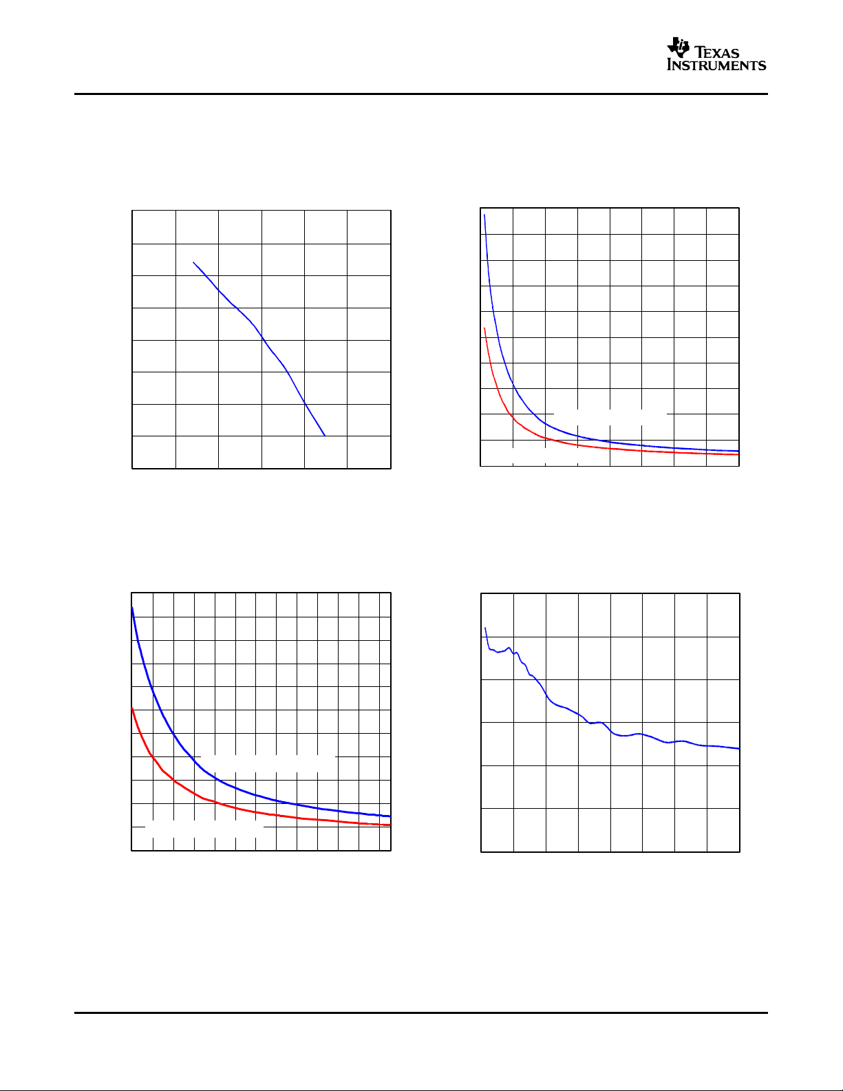
TYPICAL CHARACTERISTICS
60 80 907050
Register 4 Setting − Hex
0
1
2
3
4
5
Bandwidth − GHz
G002
A000 F010 30 4020 E0D0C0B0
25
27
29
31
33
35
37
39
41
43
45
f − Frequency − GHz
Gain − dB
0.1 101
G001
−40
−35
−30
−25
−20
−15
−10
−5
0
SDD11 − Differential Input Return Gain − dB
f − Frequency − GHz
G003
0.01 100.1 1
Differential Input Voltage − mV
PP
0
1
2
3
4
5
6
7
8
0 5 10 15 20 25 30 35 40 45 50
Random Output Jitter − ps
G004
Typical operating condition is at V
FREQUENCY RESPONSE FOR BANDWIDTH
DIFFERENT BANDWIDTH SETTINGS vs
= 3.3 V and TA= 25 ° C.
CC
REGISTER-4 SETTING
ONET4291PA
SLLS671 – SEPTEMBER 2005
DIFFERENTIAL INPUT RETURN GAIN RANDOM JITTER
FREQUENCY (MAXIMUM BANDWIDTH) INPUT AMPLITUDE (4.25 Gbps, MAXIMUM BANDWIDTH)
Figure 5. Figure 6.
vs vs
Figure 7. Figure 8.
11
Page 12
www.ti.com
0
10
20
30
40
50
60
70
80
90
100
LOS Assert/Deassert Voltage − mV
P-P
LOS Deassert Voltage
LOS Assert Voltage
G006
Register 5 Setting − Hex
0x40 0x38 0x30 0x28 0x20 0x18 0x10 0x08 0x00
VID − Differential Input Voltage − mV
P-P
0.0 0.5 1.0 1.5 2.0 2.5 3.0
Bit Error Ratio
10
-16
10
0
10
-2
10
-4
10
-6
10
-8
10
-10
10
-12
10
-14
G005
RTH − Nominal Threshold Resistor − kΩ
0
5
10
15
20
25
30
35
40
45
50
55
12 16 20 24 28 32 36 40 44 48 52 56 60
LOS Deassert Voltage
LOS Assert/Deassert Voltage − mV
PP
G013
LOS Assert Voltage
0
1
2
3
4
5
6
LOS Hysteresis − dB
G007
Register 5 Setting − Hex
0x40 0x38 0x30 0x28 0x20 0x18 0x10 0x08 0x00
ONET4291PA
SLLS671 – SEPTEMBER 2005
TYPICAL CHARACTERISTICS (continued)
Typical operating condition is at V
= 3.3 V and TA= 25 ° C.
CC
BIT-ERROR RATIO LOS ASSERT/DEASSERT VOLTAGE
vs vs
INPUT AMPLITUDE (4.25 Gbps, MAXIMUM BANDWIDTH) DIGITAL CONTROL SETTING
Figure 9. Figure 10.
LOS ASSERT/DEASSERT VOLTAGE LOS HYSTERESIS
vs vs
THRESHOLD RESISTANCE DIGITAL CONTROL SETTING
12
Figure 11. Figure 12.
Page 13

www.ti.com
RTH − Nominal Threshold Resistor − kΩ
0
1
2
3
4
5
6
12 16 20 24 28 32 36 40 44 48 52 56 60
LOS Hysteresis − dB
G014
0.0
0.5
1.0
1.5
2.0
2.5
3.0
3.5
4.0
LOS Assert Voltage Variation − dB
G008
Register 5 Setting − Hex
0x40 0x38 0x30 0x28 0x20 0x18 0x10 0x08 0x00
t − Time − 50 ps/Div
V
OD
− Differential Output Voltage − 160 mV/Div
G009
t − Time − 50 ps/Div
V
OD
− Differential Output Voltage − 160 mV/Div
G010
TYPICAL CHARACTERISTICS (continued)
Typical operating condition is at V
= 3.3 V and TA= 25 ° C.
CC
ONET4291PA
SLLS671 – SEPTEMBER 2005
LOS HYSTERESIS LOS THRESHOLD VARIATION OVER TEMPERATURE
vs vs
THRESHOLD RESISTANCE DIGITAL CONTROL SETTING
Figure 13. Figure 14.
OUTPUT EYE DIAGRAM AT 4.25 Gbps OUTPUT EYE DIAGRAM AT 4.25 Gbps
AND MINIMUM INPUT VOLTAGE (5 mV
(K28.5 PATTERN, MAXIMUM BANDWIDTH) (K28.5 PATTERN, MAXIMUM BANDWIDTH)
) AND MAXIMUM INPUT VOLTAGE (2000 mV
p-p
)
p-p
Figure 15. Figure 16.
13
Page 14

www.ti.com
t − Time − 200 ps/Div
V
OD
− Differential Output Voltage − 160 mV/Div
G012
t − Time − 200 ps/Div
V
OD
− Differential Output Voltage − 160 mV/Div
G011
ONET4291PA
SLLS671 – SEPTEMBER 2005
TYPICAL CHARACTERISTICS (continued)
Typical operating condition is at V
OUTPUT EYE DIAGRAM AT 1.0625 Gbps OUTPUT EYE DIAGRAM AT 1.0625 Gbps
AND MINIMUM INPUT VOLTAGE (5 mV
(K28.5 PATTERN, REGISTER 4 SET TO 0x70) (K28.5 PATTERN, REGISTER 4 SET TO 0x70)
= 3.3 V and TA= 25 ° C.
CC
) AND MAXIMUM INPUT VOLTAGE (2000 mV
p-p
)
p-p
Figure 17. Figure 18.
14
Page 15

www.ti.com
V
CC
V
CC
V
CC
DIN+
DIN−
DOUT−
DOUT+COC−
DIN+
DOUT−
DOUT+
SDA
GND
GND
COC+
DIN−
LOS
TH
ONET4291PA
16-Pin QFN
SCK
SD
RTHI
LOS
C
1
0.1 µF
S0099-01
C
2
0.1 µF
C
5
0.1 µF
From
Transimpedance
Amplifier (ROSA)
SDA
SCK
SD
To/From Microprocessor
R
1
10 kΩ
L
1
BLM11HA102SG
GND
C
6
0.1 µF
C
3
0.1 µF
C
4
0.1 µF
To/From
SFP
Connector
ONET4291PA
SLLS671 – SEPTEMBER 2005
APPLICATION INFORMATION
Figure 19 shows a typical application circuit using the ONET4291PA with a microprocessor for digital control of
the LOS threshold, output amplitude, and bandwidth.
Figure 19. Basic Application Circuit With Digital Control
15
Page 16

www.ti.com
V
CC
V
CC
V
CC
DIN+
DIN−
DOUT−
DOUT+COC−
DIN+
DOUT−
DOUT+
SDA
GND
GND
COC+
DIN−
LOS
TH
ONET4291PA
16-Pin QFN
SCK
SD
RTHI
LOS
C
1
0.1 µF
S0099-02
C
2
0.1 µF
C
5
0.1 µF
From
Transimpedance
Amplifier (ROSA)
R
1
10 kΩ
L
1
BLM11HA102SG
GND
C
6
0.1 µF
C
3
0.1 µF
C
4
0.1 µF
To/From
SFP
Connector
RTH
12 kΩ − 62 kΩ
ONET4291PA
SLLS671 – SEPTEMBER 2005
APPLICATION INFORMATION (continued)
Figure 20 shows a typical application without digital control. In this case, the output amplitude and bandwidth are
fixed. The LOS threshold is adjusted by means of a resistor connected to the TH terminal.
Figure 20. Basic Application Circuit With External LOS Threshold Resistor
16
Page 17

PACKAGE OPTION ADDENDUM
www.ti.com
14-Nov-2005
PACKAGING INFORMATION
Orderable Device Status
(1)
Package
Type
Package
Drawing
Pins Package
Qty
Eco Plan
ONET4291PARGVR ACTIVE QFN RGV 16 3000 Green (RoHS &
no Sb/Br)
ONET4291PARGVRG4 ACTIVE QFN RGV 16 3000 Green (RoHS &
no Sb/Br)
ONET4291PARGVT ACTIVE QFN RGV 16 250 Green (RoHS &
no Sb/Br)
ONET4291PARGVTG4 ACTIVE QFN RGV 16 250 Green (RoHS &
no Sb/Br)
(1)
The marketing status values are defined as follows:
ACTIVE: Product device recommended for new designs.
LIFEBUY: TI has announced that the device will be discontinued, and a lifetime-buy period is in effect.
NRND: Not recommended for new designs. Device is in production to support existing customers, but TI does not recommend using this part in
a new design.
PREVIEW: Device has been announced but is not in production. Samples may or may not be available.
OBSOLETE: TI has discontinued the production of the device.
(2)
Eco Plan - The planned eco-friendly classification: Pb-Free (RoHS) or Green (RoHS & no Sb/Br) - please check
http://www.ti.com/productcontent for the latest availability information and additional product content details.
TBD: The Pb-Free/Green conversion plan has not been defined.
Pb-Free (RoHS): TI's terms "Lead-Free" or "Pb-Free" mean semiconductor products that are compatible with the current RoHS requirements
for all 6 substances, including the requirement that lead not exceed 0.1% by weight in homogeneous materials. Where designed to be soldered
at high temperatures, TI Pb-Free products are suitable for use in specified lead-free processes.
Green (RoHS & no Sb/Br): TI defines "Green" to mean Pb-Free (RoHS compatible), and free of Bromine (Br) and Antimony (Sb) based flame
retardants (Br or Sb do not exceed 0.1% by weight in homogeneous material)
(2)
Lead/Ball Finish MSL Peak Temp
CU NIPDAU Level-2-260C-1 YEAR
CU NIPDAU Level-2-260C-1 YEAR
CU NIPDAU Level-2-260C-1 YEAR
CU NIPDAU Level-2-260C-1 YEAR
(3)
(3)
MSL, Peak Temp. -- The Moisture Sensitivity Level rating according to the JEDEC industry standard classifications, and peak solder
temperature.
Important Information and Disclaimer:The information provided on this page represents TI's knowledge and belief as of the date that it is
provided. TI bases its knowledge and belief on information provided by third parties, and makes no representation or warranty as to the
accuracy of such information. Efforts are underway to better integrate information from third parties. TI has taken and continues to take
reasonable steps to provide representative and accurate information but may not have conducted destructive testing or chemical analysis on
incoming materials and chemicals. TI and TI suppliers consider certain information to be proprietary, and thus CAS numbers and other limited
information may not be available for release.
In no event shall TI's liability arising out of such information exceed the total purchase price of the TI part(s) at issue in this document sold by TI
to Customer on an annual basis.
Addendum-Page 1
Page 18
Page 19
Page 20

IMPORTANT NOTICE
Texas Instruments Incorporated and its subsidiaries (TI) reserve the right to make corrections, modifications,
enhancements, improvements, and other changes to its products and services at any time and to discontinue
any product or service without notice. Customers should obtain the latest relevant information before placing
orders and should verify that such information is current and complete. All products are sold subject to TI’s terms
and conditions of sale supplied at the time of order acknowledgment.
TI warrants performance of its hardware products to the specifications applicable at the time of sale in
accordance with TI’s standard warranty. Testing and other quality control techniques are used to the extent TI
deems necessary to support this warranty. Except where mandated by government requirements, testing of all
parameters of each product is not necessarily performed.
TI assumes no liability for applications assistance or customer product design. Customers are responsible for
their products and applications using TI components. To minimize the risks associated with customer products
and applications, customers should provide adequate design and operating safeguards.
TI does not warrant or represent that any license, either express or implied, is granted under any TI patent right,
copyright, mask work right, or other TI intellectual property right relating to any combination, machine, or process
in which TI products or services are used. Information published by TI regarding third-party products or services
does not constitute a license from TI to use such products or services or a warranty or endorsement thereof.
Use of such information may require a license from a third party under the patents or other intellectual property
of the third party, or a license from TI under the patents or other intellectual property of TI.
Reproduction of information in TI data books or data sheets is permissible only if reproduction is without
alteration and is accompanied by all associated warranties, conditions, limitations, and notices. Reproduction
of this information with alteration is an unfair and deceptive business practice. TI is not responsible or liable for
such altered documentation.
Resale of TI products or services with statements different from or beyond the parameters stated by TI for that
product or service voids all express and any implied warranties for the associated TI product or service and
is an unfair and deceptive business practice. TI is not responsible or liable for any such statements.
Following are URLs where you can obtain information on other Texas Instruments products and application
solutions:
Products Applications
Amplifiers amplifier.ti.com Audio www.ti.com/audio
Data Converters dataconverter.ti.com Automotive www.ti.com/automotive
DSP dsp.ti.com Broadband www.ti.com/broadband
Interface interface.ti.com Digital Control www.ti.com/digitalcontrol
Logic logic.ti.com Military www.ti.com/military
Power Mgmt power.ti.com Optical Networking www.ti.com/opticalnetwork
Microcontrollers microcontroller.ti.com Security www.ti.com/security
Telephony www.ti.com/telephony
Video & Imaging www.ti.com/video
Wireless www.ti.com/wireless
Mailing Address: Texas Instruments
Post Office Box 655303 Dallas, Texas 75265
Copyright 2006, Texas Instruments Incorporated
 Loading...