

Page 1

OMAP5910 Dual-Core Processor
MicroWire Interface
Reference Guide
Literature Number: SPRU686
October 2003
Page 2

IMPORTANT NOTICE
Texas Instruments Incorporated and its subsidiaries (TI) reserve the right to make corrections,
modifications, enhancements, improvements, and other changes to its products and services at any
time and to discontinue any product or service without notice. Customers should obtain the latest
relevant information before placing orders and should verify that such information is current and
complete. All products are sold subject to TI’s terms and conditions of sale supplied at the time of order
acknowledgment.
TI warrants performance of its hardware products to the specifications applicable at the time of sale
in accordance with TI’s standard warranty. Testing and other quality control techniques are used to the
extent TI deems necessary to support this warranty. Except where mandated by government
requirements, testing of all parameters of each product is not necessarily performed.
TI assumes no liability for applications assistance or customer product design. Customers are
responsible for their products and applications using TI components. To minimize the risks associated
with customer products and applications, customers should provide adequate design and operating
safeguards.
TI does not warrant or represent that any license, either express or implied, is granted under any TI
patent right, copyright, mask work right, or other TI intellectual property right relating to any
combination, machine, or process in which TI products or services are used. Information published by
TI regarding third-party products or services does not constitute a license from TI to use such products
or services or a warranty or endorsement thereof. Use of such information may require a license from
a third party under the patents or other intellectual property of the third party, or a license from TI under
the patents or other intellectual property of TI.
Reproduction of information in TI data books or data sheets is permissible only if reproduction is without
alteration and is accompanied by all associated warranties, conditions, limitations, and notices.
Reproduction of this information with alteration is an unfair and deceptive business practice. TI is not
responsible or liable for such altered documentation.
Resale of TI products or services with statements different from or beyond the parameters stated by
TI for that product or service voids all express and any implied warranties for the associated TI product
or service and is an unfair and deceptive business practice. TI is not responsible or liable for any such
statements.
Following are URLs where you can obtain information on other Texas Instruments products and
application solutions:
Products Applications
Amplifiers amplifier.ti.com Audio www.ti.com/audio
Data Converters dataconverter.ti.com Automotive www.ti.com/automotive
DSP dsp.ti.com Broadband www.ti.com/broadband
Interface interface.ti.com Digital Control www.ti.com/digitalcontrol
Logic logic.ti.com Military www.ti.com/military
Power Mgmt power.ti.com Optical Networking www.ti.com/opticalnetwork
Microcontrollers microcontroller.ti.com Security www.ti.com/security
Telephony www.ti.com/telephony
Video & Imaging www.ti.com/video
Wireless www.ti.com/wireless
Mailing Address: Texas Instruments
Post Office Box 655303 Dallas, Texas 75265
Copyright 2003, Texas Instruments Incorporated
Page 3

About This Manual
This serial synchronous interface can drive two serial external components.
For the external devices, this interface is compatible with the MicroWire
standard and is seen as the master.
Notational Conventions
This document uses the following conventions.
- Hexadecimal numbers are shown with the suffix h. For example, the
Preface
Read This First
following number is 40 hexadecimal (decimal 64): 40h.
Related Documentation From Texas Instruments
The following documents describe the OMAP5910 device and related
peripherals. Copies of these documents are available on the Internet at
www.ti.com. Tip: Enter the literature number in the search box provided at
www.ti.com.
OMAP5910 Dual-Core Processor MPU Subsystem Reference Guide (litera-
ture number SPRU671)
OMAP5910 Dual-Core Processor DSP Subsystem Reference Guide
(literature number SPRU672)
OMAP5910 Dual-Core Processor Memory Interface Traffic Controller
Reference Guide (literature number SPRU673)
OMAP5910 Dual-Core Processor System D MA Controller Reference Guide
(literature number SPRU674)
OMAP5910 Dual-Core Processor LCD Controller Reference Guide (litera-
ture number SPRU675)
OMAP5910 Dual-Core Processor Universal Asynchronous
Receiver/Transmitter ( U A RT) Devices Reference Guide (literature number
SPRU676)
5OMAP5910SPRU686
Page 4

Trademarks
Related Documentation From Texas Instruments / Trademarks
OMAP5910 Dual-Core Processor Universal Serial Bus (USB) and Frame
Adjustment Counter (FAC) Reference Guide (literature number SPRU677)
OMAP5910 Dual-Core Processor Clock Generation and System Reset
Management Reference Guide (literature number SPRU678)
OMAP5910 Dual-Core Processor General-Purpose Input/Output (GPIO)
Reference Guide (literature number SPRU679)
OMAP5910 Dual-Core Processor MMC/SD Reference Guide (literature
number SPRU680)
OMAP5910 Dual-Core Processor Inter-Integrated Circuit (I2C) Controller
Reference Guide (literature number SPRU681)
OMAP5910 Dual-Core Processor Timer Reference Guide (literature number
SPRU682)
OMAP5910 Dual-Core Processor Inter-Processor Communication
Reference Guide (literature number SPRU683)
OMAP5910 Dual-Core Processor Camera Interface Reference Guide
(literature number SPRU684)
OMAP5905 Dual-Core Processor Multichannel Serial Interface (MCSI)
Reference Guide (literature number SPRU685)
OMAP5910 Dual-Core Processor Micro-Wire Interface Reference Guide
(literature number SPRU686)
OMAP5910 Dual-Core Processor Real-Time Clock (RTC) Reference Guide
(literature number SPRU687)
OMAP5910 Dual-Core Processor HDQ/1-Wire Interface Reference Guide
(literature number SPRU688)
OMAP5910 Dual-Core Processor PWL, PWT, and LED Peripheral
Reference Guide (literature number SPRU689)
OMAP5910 Dual-Core Processor Multi ch an ne l B u f f er ed Seria l Port ( M cB SP )
Reference Guide (literature number SPRU708)
Trademarks
OMAP and the OMAP symbol are trademarks of Texas Instruments.
6 OMAP5910 SPRU686
Page 5

Contents
Contents
1 MicroWire Interface 11. . . . . . . . . . . . . . . . . . . . . . . . . . . . . . . . . . . . . . . . . . . . . . . . . . . . . . . . . . . . . . .
1.1 MicroWire Registers 11. . . . . . . . . . . . . . . . . . . . . . . . . . . . . . . . . . . . . . . . . . . . . . . . . . . . . . . . .
1.2 Protocol Description 19. . . . . . . . . . . . . . . . . . . . . . . . . . . . . . . . . . . . . . . . . . . . . . . . . . . . . . . . .
1.3 Example of Protocol Using a Serial EEPROM (XL93LC66) 21. . . . . . . . . . . . . . . . . . . . . . . .
1.3.1 Read Cycle 21. . . . . . . . . . . . . . . . . . . . . . . . . . . . . . . . . . . . . . . . . . . . . . . . . . . . . . . . . .
1.3.2 Write Cycle 22. . . . . . . . . . . . . . . . . . . . . . . . . . . . . . . . . . . . . . . . . . . . . . . . . . . . . . . . . .
1.4 Example of Protocol Using an LCD Controller (COP472-3) 23. . . . . . . . . . . . . . . . . . . . . . . .
1.4.1 Loading Sequence 23. . . . . . . . . . . . . . . . . . . . . . . . . . . . . . . . . . . . . . . . . . . . . . . . . . . .
1.5 Example of Protocol Using the Autotransmit Mode 24. . . . . . . . . . . . . . . . . . . . . . . . . . . . . . .
1.6 Example of the Autotransmit Mode With DMA Support 26. . . . . . . . . . . . . . . . . . . . . . . . . . . .
Figures
1 Block Diagram 11. . . . . . . . . . . . . . . . . . . . . . . . . . . . . . . . . . . . . . . . . . . . . . . . . . . . . . . . . . . . . . . . .
2 Behavior of a X25C02 EEPROM Read Cycle 20. . . . . . . . . . . . . . . . . . . . . . . . . . . . . . . . . . . . . .
3 Behavior of a XL93LC66 EEPROM Read Cycle 20. . . . . . . . . . . . . . . . . . . . . . . . . . . . . . . . . . . .
4 Read Cycle in the Autotransmit Mode 26. . . . . . . . . . . . . . . . . . . . . . . . . . . . . . . . . . . . . . . . . . . . .
Tables
1 MicroWire Registers 11. . . . . . . . . . . . . . . . . . . . . . . . . . . . . . . . . . . . . . . . . . . . . . . . . . . . . . . . . . .
2 Transmit-Data Register (TDR) 12. . . . . . . . . . . . . . . . . . . . . . . . . . . . . . . . . . . . . . . . . . . . . . . . . . .
3 Receive-Data Register (RDR) 12. . . . . . . . . . . . . . . . . . . . . . . . . . . . . . . . . . . . . . . . . . . . . . . . . . .
4 Control-and-Status Register (CSR) 13. . . . . . . . . . . . . . . . . . . . . . . . . . . . . . . . . . . . . . . . . . . . . .
5 Setup Register 1 (SR1) 14. . . . . . . . . . . . . . . . . . . . . . . . . . . . . . . . . . . . . . . . . . . . . . . . . . . . . . . .
6 Setup Register 2 (SR2) 16. . . . . . . . . . . . . . . . . . . . . . . . . . . . . . . . . . . . . . . . . . . . . . . . . . . . . . . . .
7 Setup Register 3 (SR3) 17. . . . . . . . . . . . . . . . . . . . . . . . . . . . . . . . . . . . . . . . . . . . . . . . . . . . . . . . .
8 Setup Register 4 (SR4) (Read/Write) 18. . . . . . . . . . . . . . . . . . . . . . . . . . . . . . . . . . . . . . . . . . . . .
9 Setup Register 5 (SR5) (Read/Write) 18. . . . . . . . . . . . . . . . . . . . . . . . . . . . . . . . . . . . . . . . . . . . .
7SPRU686
Page 6

8 SPRU686
Page 7
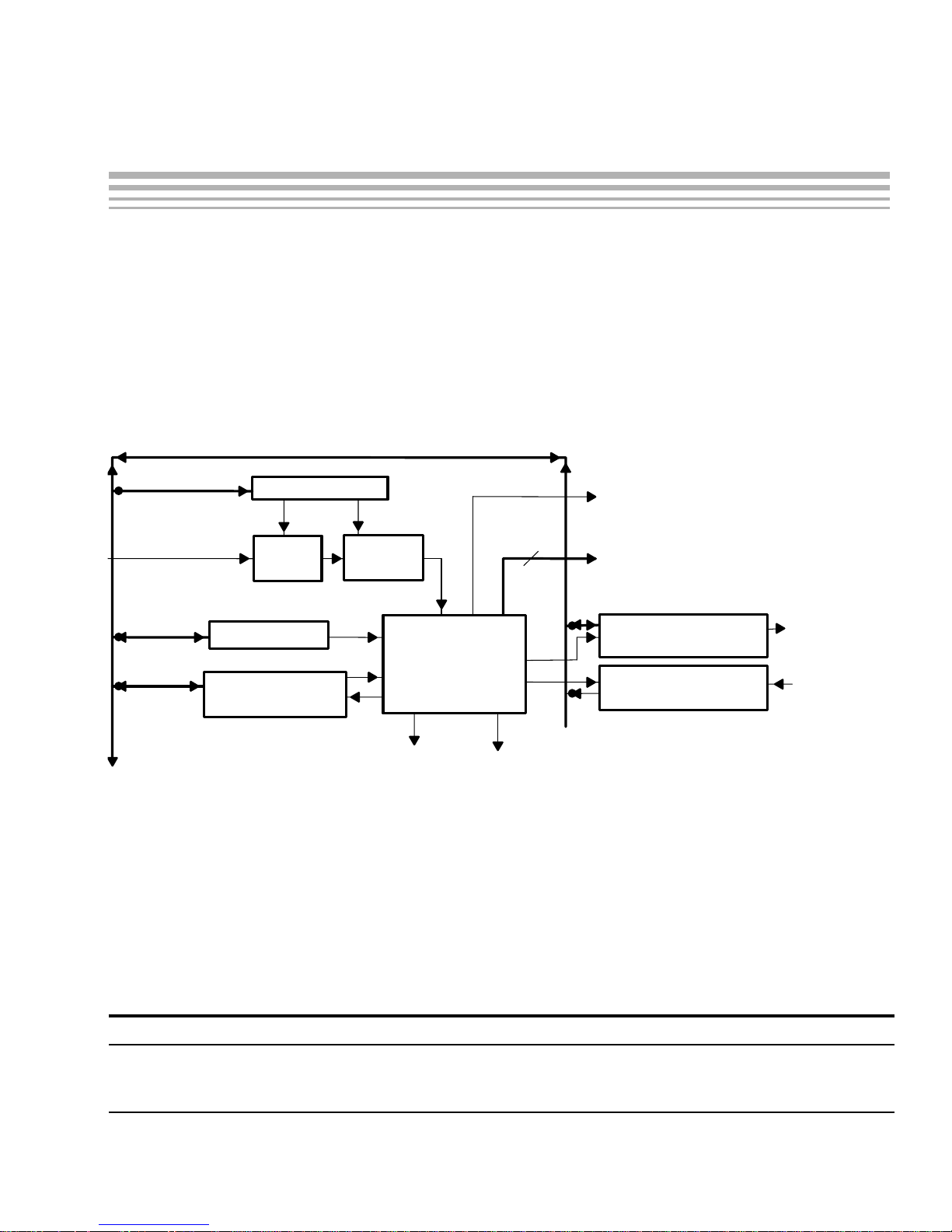
1 MicroWire Interface
This serial synchronous interface can drive two serial external components.
For the external devices, this interface is compatible with the MicroWire
standard and is seen as the master (see Figure 1).
A transmit DMA mode is available.
Figure 1. Block Diagram
MicroWire Interface
Clock register
MPUXOR_CK
IPB
Clock
enable
Setup registers
Control−and−status
register
Clock
divider
UWIRE.CS[3:0]
1.1 MicroWire Registers
The starting address in the peripheral range (hex) is FFFB:3000
Table 1 lists the MicroWire registers. Table 2 through Table 9
describe the individual registers.
Control
logic
2
UWIRE.SCLK
DMA_REQ to system DMA_REQ[6:0]
Inth lvl2 (2,3) - edge
Transmit data register
(16 bits)
Receive data register
(16 bits)
UWIRE.SDO
UWIRE.SDI
Table 1. MicroWire Registers
Register Description R/W Size Address Offset
TDR Transmit data register W 16 bits FFFB:3000 0x00
RDR Receive data register R 16 bits FFFB:3000 0x00
9MicroWire InterfaceSPRU686
Page 8

MicroWire Interface
Table 1. MicroWire Registers (Continued)
Register OffsetAddressSizeR/WDescription
CSR Controland status register R/W 16 bits FFFB:3000 0x04
SR1 Setup register 1 R/W 16 bits FFFB:3000 0x08
SR2 Setup register 2 R/W 16 bits FFFB:3000 0x0C
SR3 Setup register 3 R/W 16 bits FFFB:3000 0x10
SR4 Setup register 4 R/W 16 bits FFFB:3000 0x14
SR5
Setup register 5 R/W 16 bits FFFB:3000 0x18
Table 2. Transmit-Data Register (TDR)
Bits Field Description
15−0 TD Data to transmit Undefined
Whatever its size, the word must be aligned on the most significant bit (MSB)
side.
Note:
The MSB (bit 15) is the first transmitted bit.
Reset
Value
Table 3. Receive-Data Register (RDR)
Bits Field Description
15−0 RD Received data Undefined
Whatever its size, the word is aligned on the least significant bit (LSB) side.
Note:
The LSB (bit 0) is the last received bit.
MicroWire Interface10 SPRU686
Reset
Value
Page 9

Table 4. Control-and-Status Register (CSR)
Bits Field Value Description
MicroWire Interface
Reset
Value
15 RDRB RDRB bit = 1 indicates that the receive (RDR) area is full.
When the controller reads the content of the RDR, this bit
is cleared.
This bit is read only.
14 CSRB CSRB bit = 0 indicates that the control and status register
(CSR) is ready to receive new data.
After starting a MicroWire transfer with the CSR, this bit is
set to 1. When the corresponding action has been done,
the CSRB is reset. This bit is controlled by a MicroWire
internal state machine running on the F_INT internal clock
(12 MHz/N). If the CSR is read just after being written and
the MPU is running at a high frequency (60 MHz or 120
MHz, for instance) compared to the internal clock, the
CSRB status bit may still be low for the first read access.
The CSRB latency is 0 if the transfer was initiated by
modifying the CS_CMD bit, but it can be 0−3 cycles if
initiated by the START bit. Some suggested work-arounds
are to: (a) have a few NOPs between initiating a MicroWire
transfer and checking the CSRB status or( b) check that
the CSRB first has a high value on an initial read before it
goes low on a subsequent read.
This bit is read only.
0
0
13 START 1 Start a write and/or a read process.
This bit is automatically reset by the internal logic when a
write or a read process is activated.
Send the NB_BITS_WR bits (contained in TDR) to the
serial output DO. If the NB_BITS_WR is equal to zero,
then the write process is not started.
Receive the NB_BITS_RD bits from the serial input DI and
store them in the RDR.
12 CS_CMD 1 Set the chip-select of the selected device to its active level. 0
11−10 INDEX Index of the external device Undefined
00 CS0
01 Reserved
10 Reserved
11 CS3
0
11MicroWire InterfaceSPRU686
Page 10

MicroWire Interface
Table 4. Control-and-Status Register (CSR) (Continued)
Reset
Bits
9−5 NB_BITS_WR Number of bits to transmit Undefined
4−0 NB_BITS_RD Number of bits to receive Undefined
DescriptionValueField
Value
This register sets up the serial interface for the first and the second external
components.
Table 5. Setup Register 1 (SR1)
Bits Field Value Description
11−6 Reserved
Reset
Value
5 CS0_CHK Before activating a write process, determines if the
external device is ready.
0 No check is done and the write process is immediately
executed.
1 If the DI signal is low, the interface considers the
external component busy; if the DI is high, the interface
considers that the first external component is ready and
starts the write process.
Used when the CS0 is selected.
4−3 CS0_FRQ Defines the frequency of the serial clock, SCLK, when
the CS0 is selected (F_INT is the frequency of the
internal clock to the MicroWire control logic as defined in
register SR3).
00 F_INT/2
01 F_INT/4
10 F_INT/8
11 Reserved
Undefined
Undefined
2
CS0CS_LVL Defines the active level of the chip-select by CS0 0
MicroWire Interface12 SPRU686
Page 11

Table 5. Setup Register 1 (SR1) (Continued)
Bits
DescriptionValueField
MicroWire Interface
Reset
Value
1 CS0_EDGE_WR When the CS0 is selected, this bit defines the active
edge of the serial clock, SCLK, used to write data to the
serial input D0. (Output data is generated on this edge)
0 Falling (the serial clock is not inverted)
0 Rising (when the serial clock is inverted)
1 Rising (the serial clock is not inverted)
1 Falling (when the serial clock is inverted)
0 CS0_EDGE_RD When the CS0 is selected, this bit defines the active
edge of the serial clock, SCLK, used to read data from
the serial input DI. (Input data is strobed on this edge)
0 Falling (the serial clock is not inverted)
0 Rising (when the serial clock is inverted)
1 Rising (the serial clock is not inverted)
1 Falling (when the serial clock is inverted)
Note:
Undefined
Undefined
The content of this register must not be changed when a read or write process is running.
This register sets up the serial interface for the first and the second external
components.
13MicroWire InterfaceSPRU686
Page 12

MicroWire Interface
Table 6. Setup Register 2 (SR2)
Bits Field Value Description
Reset
Value
11 CS3_CHK Before activating a write process, determines
if the external device is ready.
0 No check is done and the write process is
immediately executed.
1 If the DI signal is low, the interface considers
the external component busy; if the DI is high,
the interface considers that the first external
component is ready and starts the write
process.
Used when the CS3 is selected.
10−9 CS3_FRQ Defines the frequency of the serial clock,
SCLK, when the CS3 is selected
00 F_INT/2
01 F_INT/4
10 F_INT/8
11 Undefined
8 CS3CS_LVL Defines the active level of the CS3 chip-select 0
Undefined
Undefined
7 CS3_EDGE_WR When the CS3 is selected, this bit defines the
active edge of the serial clock, SCLK, used to
write data to the serial input D0. (Output data
is generated on this edge)
0 Falling (the serial clock is not inverted)
0 Rising (when the serial clock is inverted)
1 Rising (the serial clock is not inverted)
1 Falling (when the serial clock is inverted)
MicroWire Interface14 SPRU686
Undefined
Page 13

Table 6. Setup Register 2 (SR2)
Bits
MicroWire Interface
Reset
DescriptionValueField
Value
6 CS3_EDGE_RD When the CS3 is selected, this bit defines the
active edge of the serial clock, SCLK, used to
read data from the serial input DI. (Input data
is strobed on this edge)
0 Falling (the serial clock is not inverted)
0 Rising (when the serial clock is inverted)
1 Rising (the serial clock is not inverted)
1 Falling (when the serial clock is inverted)
5−0
Reserved
Note:
The content of this register must not be changed when a read or write process is running.
This register sets up the serial interface for the internal clock.
Table 7. Setup Register 3 (SR3)
Undefined
Bits Field Value Description
2−1 CK_FREQ Defines the frequency of the internal clock, F_INT, when
the CLK_EN = 1. All the internal logic is controlled by
F_INT (F is the frequency of the external input clock).
00 MPUOXR_CK/2
01 MPUOXR_CK/4
10 MPUOXR_CK/7
11 MPUOXR_CK/10
0 CLK_EN 0 Switch off the clock 0
1 Switch on the clock
Note:
The content of this register must not be changed when a read or write process is running.
Reset
Value
00
15MicroWire InterfaceSPRU686
Page 14

MicroWire Interface
This register sets up the serial-clock polarity.
Table 8. Setup Register 4 (SR4) (Read/Write)
Bits Field Value Description
Reset
Value
0 CLK_IN 0
The serial clock is not inverted
1
The serial clock is inverted
Note:
Content of this register must not be changed when a read or write process is running.
Table 9. Setup Register 5 (SR5) (Read/Write)
Bits Field Value Description
3 CS_TOGGLE_TX_EN CS_TOGGLE_TX_EN is possible only in the
autotransmit mode.
When in the autotransmit mode with
CS_TOGGLE_TX_EN inactive, the CS does not
go to its active level automatically. Control the CS
with the CS_CMD bit of the control and status
register (CSR) in the software.
0
Reset
Value
0
2 AUTO_TX_EN In the autotransmit mode, the CS_CMD and
MicroWire Interface16 SPRU686
0 The CS_toggle transmit mode is disabled.
1 The CS_toggle transmit mode is enabled.
0
START bits of the control and status register
(CSR) are not used. A hardware state machine
detects a TXD write and automatically sets the
programmed CS to its active value, then starts
the transmission.
The CS_CMD and the START bits in the control
and status register (CSR) are not updated during
the autotransmit mode.
0 The autotransmit mode is disabled.
1 The autotransmit mode is enabled.
Page 15

Table 9. Setup Register 5 (SR5) (Read/Write)
Bits
DescriptionValueField
MicroWire Interface
Reset
Value
1 IT_EN In the IT mode, an interrupt is generated each
time a word has been transferred or received.
This interrupt is a negative edge-triggered
interrupt. A status register (IST) allows the CPU
to know which interrupt (receive or/and transmit)
occurred.
0 The IT mode is disabled.
1 The IT mode is enabled.
0 DMA_TX_EN 0 The DMA transmit mode is disabled. 0
1 The DMA transmit mode is enabled.
Note:
The content of this register must not be changed when a read or write
process is running.
Set up the DMA, IT, AUTO_TX, and CS_TOGGLE modes in this register.
In the DMA mode, a DMA request is initiated each time a transmission slot is
available.
0
The maximum word size in the DMA mode is 16 bits.
Notes:
Another CS cannot be used in the normal or DMA mode when a DMA mode
is active on one specific CS.
To use the MicroWire in the DMA transmit modes, the DMA_EN and
AUTO_TX_EN must be enabled, and IT_EN is best disabled. The
AUTO_TX_EN can be active when the DMA_EN is disabled.
1.2 Protocol Description
The serial port must be configured in order to use the setup registers.
This interface can only drive one device at a given time. Therefore, the
chip-select of the selected device must be set to its active level before starting
any read or write process.
17MicroWire InterfaceSPRU686
Page 16

MicroWire Interface
After the loading of the transmit data register (TDR), a write process is
activated by setting the START bit to 1 and by writing a value different from zero
to the NB_BITS_WR field.
A read process is always simultaneous with a write process, which means that
at every serial clock, SCLK, cycle data is read. After having finished a write
process (if necessary), a number (defined by the NB_BITS_RD) of SCLK
cycles is generated to allow the storage of data from the serial input DI.
The transmitted data word is shifted out on the rising or falling edge of the serial
clock (according to the value of the CSx_EDGE_WR bits of the setup
registers). The received data word is shifted in on the falling or rising edge of
the serial clock (according to the value of the CSx_EDGE_RD bits of the setup
registers). When the CSx_EDGE_WR and CSx_EDGE_RD bits have the
same value, it is assumed that the device behavior is the one shown in
Figure 2. Otherwise, the required behavior of the external device is shown in
Figure 3.
Figure 2. Behavior of a X25C02 EEPROM Read Cycle
WIRE_NCS
UWIRE.SCLK
UWIRE.SDO
UWIRE.SDI
000000 A7
1 1 A6 A5 A4 A3 A2 A1 A0
On the DO line, data is generated from the MicroWire interface on the SLCK
falling edge and read by the EEPROM interface on the SCLK rising edge.
On the DI line, data is generated from the EEPROM interface on the SCLK
falling edge and read by the MicroWire interface on the SCLK falling edge.
Figure 3. Behavior of a XL93LC66 EEPROM Read Cycle
WIRE_NCS
UWIRE_SCLK
UWIRESDO
UWIRE_SDI
110
A7 A6 A5 A4 A3 A2 A1 A0
D15
D6 D5 D4 D1 D0
D7
D14 D13 D1 D0
On the DO line, data is generated from the MicroWire interface on the SLCK
falling edge and read by the EEPROM interface on the SCLK rising edge.
MicroWire Interface18 SPRU686
Page 17

MicroWire Interface
On the DI line, data is generated from the EEPROM interface on the SCLK
rising edge and read by the MicroWire interface on the SCLK rising edge.
1.3 Example of Protocol Using a Serial EEPROM (XL93LC66)
Set up the interface by writing the following values in setup register 1 (SR1):
- CS_EDGE_RD = 1
- CS_EDGE_WR = 0
- CSCS_LVL = 1
- CS_FRQ = 00
- CS_CHK = 1
In this example, only two cycles (read and write) are described.
1.3.1 Read Cycle
1) Set the following fields of the control and status register (CSR):
J NB_BITS_RD: 0
J NB_BITS_WR: 0
J INDEX: 00
J CS_CMD: 1
J START: 0
2) Load the transmit data register (TDR) with:
J 1 1 0 A7 A6 A5 A4 A3 A2 A1 A0 x x x x x x: Don’t care
J A7 ... A0: Address of the selected memory register
3) Wait for the CSRB bit of the CSR to be reset.
4) Set the following fields of the control and status register (CSR):
J NB_BITS_RD: 16 (decimal)
J NB_BITS_WR: 11 (decimal)
J INDEX: 00
J CS_CMD: 1
J START: 1
5) Wait until the CSRB = 0 and RDRB = 1 (status bits of the CSR).
6) Read the content of the receive data register (RDR).
7) To continue reading the data external component, the EEPROM, go to 8.
Else go to 9.
19MicroWire InterfaceSPRU686
Page 18

MicroWire Interface
1.3.2 Write Cycle
8) Set the following fields of the control and status register (CSR):
J NB_BITS_RD: 16 (decimal)
J NB_BITS_WR: 0 (decimal)
J INDEX: 00
J CS_CMD: 1
J START: 1
J Go to 5.
9) Set the following fields of the control and status register (CSR):
J INDEX: 00
J CS_CMD: 0
J START: 0
1) Set the following fields of the control and status register (CSR):
J NB_BITS_RD: 0
J NB_BITS_WR: 0
J INDEX: 00
J CS_CMD: 1
J START: 0
2) Load the transmit data register (TDR) with:
J 1 0 1 A7 A6 A5 A4 A3 A2 A1 A0 x x x x x x: Don’t care
J A7 ... A0: Address of the selected memory register
3) Wait for the CSRB bit of the control and status register (CSR) to be reset.
4) Set the following fields of the control and status register (CSR):
J NB_BITS_RD: 0
J NB_BITS_WR: 11 (decimal)
J INDEX: 00
J CS_CMD: 1
J START: 1
5) Wait for the CSRB bit of the control and status register (CSR) to be reset.
6) Load the transmit data register (TDR) with:
J D15 D14 ... D0
J D15 ... D0: Data
MicroWire Interface20 SPRU686
Page 19

MicroWire Interface
7) Set the following fields of the control and status register (CSR):
J NB_BITS_RD: 0
J NB_BITS_WR: 16 (decimal)
J INDEX: 00
J CS_CMD 1
J START: 1
8) Wait for the CSRB bit of the CSR to be reset.
9) Set the following fields of the control and status register (CSR):
J INDEX: 00
J CS_CMD: 0
J START: 0
1.4 Example of Protocol Using an LCD Controller (COP472-3)
Set up the interface by writing in the setup register 1 (SR1) the following value:
J CS_EDGE_RD = 1
J CS_EDGE_WR = 0
J CSCS_LVL = 0
J CS_FRQ = 10
J CS_CHK = 0
This example describes a loading sequence to drive a four-digit display.
1.4.1 Loading Sequence
1) Set the following fields of the control and status register (CSR):
J NB_BITS_RD: 0
J NB_BITS_WR: 0
J INDEX: 01
J CS_CMD: 1
J START: 0
2) Wait for the CSRB bit of the control and status register (CSR) to be reset.
3) Load the transmit data register (TDR) with:
J D7d1...D0d1 D7d2...D0d2 D7d1...D0d1: Data for digit 1
J D7d2...D0d2: Data for digit 2
4) Set the following fields of the control and status register (CSR):
J NB_BITS_RD: 0
J NB_BITS_WR: 16 (decimal)
J INDEX: 01
J CS_CMD: 1
J START: 1
21MicroWire InterfaceSPRU686
Page 20

MicroWire Interface
5) Wait for the CSRB bit of the control and status register (CSR) to be reset.
6) Load the transmit data register (TDR) with:
J D7d3...D0d3 D7d4...D0d4 D7d3...D0d3: Data for digit 3
J D7d4...D0d4: Data for digit 4
7) Set the following fields of the control and status register (CSR):
J NB_BITS_RD: 0
J NB_BITS_WR: 16 (decimal)
J INDEX: 01
J CS_CMD: 1
J START: 1
8) Wait for the CSRB bit of the control and status register (CSR) to be reset.
9) Load the transmit data register (TDR) with:
J D7...D0 x x x x x x x x x: Don’t care
J D7...D0: Data for the special segment and control function
10) Set the following fields of the control and status register (CSR):
J NB_BITS_RD: 0
J NB_BITS_WR: 8 (decimal)
J INDEX: 01
J CS_CMD: 1
J START: 1
11) Wait for CSRB to go low, which indicates the CSR is ready to receive new
data. It is advised to read the bit before and after every write access to the
CSR to check the status.
12) Set the following fields of the control and status register (CSR):
J INDEX: 01
J CS_CMD: 0
J START: 0
1.5 Example of Protocol Using the Autotransmit Mode
The autotransmit mode is controlled by the setup register 5 (SR5). The
following example configures the MicroWire for a read access on the CS0 with
the serial clock out inverted, the CS autotoggle enabled, the DMA request
disabled, and the interrupt enabled:
MicroWire Interface22 SPRU686
Page 21

MicroWire Interface
1) SR5 = DMA_TX_EN: 0
IT_EN: 1
AUTO_TX_EN: 1
CS_TOGGLE_TX_EN: 1
2) SR1 = CS0_EDGE_RD: 0
CS0_EDGE_WR: 1
CS0CS_LVL: 0
CS0_FREQ: 00
CS0_CHK: 1
Note:
The data out is latched on the falling edge of the serial clock. The data in is
sampled on the rising edge.
3) SR3 = CLK_EN: 1
CK_FREQ: 00 (must wait for 1 external clock + 1 F_INT cycle before any
other register access)
4) SR4 = CLK_IN: 1
5) Set the following fields of the control and status register (CSR):
J NB_BITS_RD: 5
J NB_BITS_WR: 7
J INDEX: 00
J CS_CMD: 0
J START: 0
6) Wait for the CSRB = 0 of the control and status register (CSR).
7) Load the transmit data register (TDR) with:
J A6 A5 A4 A3 A2 A1 A0 x x x x x x x x x x: Don’t care
J A6 ... A0: Address of the selected memory register
The transfer is automatically started.
8) Wait until the CSRB = 0 and RDRB = 1 (status bits of CSR).
9) Read the content of the receive data register (RDR).
10) To continue reading the data external component, go to 5 else go to 11.
23MicroWire InterfaceSPRU686
Page 22

MicroWire Interface
11) Release the autotransmit mode: SR5 = AUTO_TX_EN: 0.
12) END
The corresponding behavior of the serial interface is described in Figure 4.
Figure 4. Read Cycle in the Autotransmit Mode
WIRE_NCS
UWIRE_SCCLK
UWIRE_SDO
UWIRE_SDI
A6 A5 A4 A3 A2 A1 A0
D4 D3 D2 D1 D0
1.6 Example of the Autotransmit Mode With DMA Support
The autotransmit mode and DMA mode are controlled by the setup register 5
(SR5). The following example configures the MicroWire for a 16-bit write
access on the CS1 with the serial clock out not inverted, the CS auto toggle
enabled, the DMA request enabled, and the interrupt disabled:
1) Set up and enable the DMA channel.
2) Program the configuration registers SR1, SR3, and SR4.
3) Check the CSRB status to ensure that the peripheral is ready to receive
(low).
4) Program the control and status register (CSR) as follows:
J NB_BITS_RD = 0
J NB_BITS_WR = 16
J INDEX = 00
J CS_CMD: = 1
J START = 0
5) Write to the setup register 5 (SR5) to configure and initiate the transfer:
J DMA_TX_EN = 1
J IT_EN = 0
J AUTO_TX_EN = 1
J CS_TOGGLE_TX_EN = 1 (In AUTO TX mode, setting the
MicroWire Interface24 SPRU686
DMA_TX_EN bit to 1 starts the transfer)
Page 23

MicroWire Interface
6) When the DMA transfer is complete, check the status of the CSRB to find
whether or not the MicroWire has finished the serial data transfer.
7) Write to the setup register (SR5) to disable DMA and AUTO TX mode:
J DMA_TX_EN = 0
J IT_EN = 0
J AUTO_TX_EN = 0
J CS_TOGGLE_TX_EN = 0
Using Autostart and Autotoggle CS Mode
A minimum wait period of 2 x F_INT clock cycles must occur after
the end of the transfer (transition 1 to 0 detected on the CSRB)
before setting the SR3 register to turn off the internal clock.
25MicroWire InterfaceSPRU686
Page 24

MicroWire Interface26 SPRU686
Page 25

Index
Index
A
autotransit mode protocol 22
E
EEPROM interface, protocol, MicroWire
interface 18
example, protocol
autotransit mode 22
LCD controller 21
serial EEPROM 19
I
interface, MicroWire 9
L
LCD controller, protocol 21
M
MicroWire interface, MPU public peripherals 9
MPU public peripherals, MicroWire interface
protocol 17
registers 9
P
protocol
autotransit mode, example 22
LCD controller, example 21
MicroWire interface 17
serial EEPROM, example 19
S
serial EEPROM protocol 19
27SPRU686
Page 26

28 SPRU686
 Loading...