

Texas Instruments MSP430G2533, MSP430G2433, MSP430G2333, MSP430G2233, MSP430G2403 Datasheet
...
Product
Folder
Sample &
Buy
Technical
Documents
Tools &
Software
Support &
Community
Reference
Design
MSP430G2533,MSP430G2433,MSP430G2333,MSP430G2233
MSP430G2x33, MSP430G2x03 Mixed-Signal Microcontrollers
1 Device Overview
1.1 Features
1
• Low Supply-Voltage Range: 1.8 V to 3.6 V
• Ultra-Low Power Consumption
– Active Mode: 230 µA at 1 MHz, 2.2 V
– Standby Mode: 0.5 µA
– Off Mode (RAM Retention): 0.1 µA
• Five Power-Saving Modes
• Ultra-Fast Wake up From Standby Mode in Less
Than 1 µs
• 16-Bit RISC Architecture, 62.5-ns Instruction Cycle
Time
• Basic Clock Module Configurations
– Internal Frequencies up to 16 MHz With Four
Calibrated Frequencies
– Internal Very-Low-Power Low-Frequency (LF)
Oscillator
– 32-kHz Crystal
– External Digital Clock Source
• Two 16-Bit Timer_A With Three Capture/Compare
Registers
• Up to 24 Capacitive-Touch Enabled I/O Pins
MSP430G2403, MSP430G2303, MSP430G2203
SLAS734G –APRIL 2011–REVISED APRIL 2016
• Universal Serial Communication Interface (USCI)
– Enhanced UART Supports Automatic Baud-
Rate Detection (LIN)
– IrDA Encoder and Decoder
– Synchronous SPI
– I2C
• 10-Bit 200-ksps Analog-to-Digital Converter (ADC)
With Internal Reference, Sample-and-Hold, and
Autoscan (See Table 3-1)
• Brownout Detector
• Serial Onboard Programming,
No External Programming Voltage Needed,
Programmable Code Protection by Security Fuse
• On-Chip Emulation Logic With Spy-Bi-Wire
Interface
• Section 3 Summarizes Available Family Members
• Package Options
– TSSOP: 20 Pin, 28 Pin
– PDIP: 20 Pin
– QFN: 32 Pin
• For Complete Module Descriptions, See the
MSP430x2xx Family User’s Guide (SLAU144)
1.2 Applications
• Power Management
• Sensor Interface
1.3 Description
The TI MSP family of ultra-low-power microcontrollers consists of several devices that feature different
sets of peripherals targeted for various applications. The architecture, combined with five low-power
modes, is optimized to achieve extended battery life in portable measurement applications. The device
features a powerful 16-bit RISC CPU, 16-bit registers, and constant generators that contribute to
maximum code efficiency. The digitally controlled oscillator (DCO) allows the device to wake up from lowpower modes to active mode in less than 1 µs.
The MSP430G2x03 and MSP430G2x33 devices are ultra-low-power mixed-signal microcontrollers with
built-in 16-bit timers, up to 24 I/O capacitive-touch enabled pins, and built-in communication capability
using the USCI. In addition, the MSP430G2x33 family members have a 10-bit ADC. See Section 3 for
configuration details.
Typical applications include low-cost sensor systems that capture analog signals, convert them to digital
values, and then process the data for display or for transmission to a host system.
1
• Capacitive Touch
An IMPORTANT NOTICE at the end of this data sheet addresses availability, warranty, changes, use in safety-critical applications,
intellectual property matters and other important disclaimers. PRODUCTION DATA.

Clock
System
Brownout
Protection
RST/NMI
DVCC DVSS
MCLK
Watchdog
WDT+
15-Bit
Timer0_A3
3 CC
registers
16-MHz
CPU
including
16 registers
Emulation
2BP
JTAG
interface
SMCLK
ACLK
Port P1
8 I/Os,
interrupt
capability,
pullup or
pulldown
resistors
P1.x
8
P2.x
Port P2
8 I/Os,
interrupt
capability,
pullup or
pulldown
resistors
Spy-Bi-
Wire
Timer1_A3
3 CC
registers
XIN
XOUT
Port P3
8 I/Os,
pullup or
pulldown
resistors
P3.x
8 8
RAM
512B
256B
Flash
16KB
8KB
4KB
2KB
USCI A0
UART,
LIN, IrDA,
SPI
USCI B0
SPI, I C
2
ADC
10 bit,
8 channel,
autoscan,
1-channel
DMA
MDB
MAB
Copyright © 2016, Texas Instruments Incorporated
MSP430G2533,MSP430G2433,MSP430G2333,MSP430G2233
MSP430G2403, MSP430G2303, MSP430G2203
SLAS734G –APRIL 2011–REVISED APRIL 2016
www.ti.com
PART NUMBER PACKAGE BODY SIZE
MSP430G2533IRHB VQFN (32) 5 mm × 5 mm
MSP430G2533IPW
MSP430G2533IN PDIP (20) 24.33 mm × 6.35 mm
(1) For the most current part, package, and ordering information, see the Package Option Addendum in
Section 8, or see the TI website at www.ti.com.
(2) The sizes shown here are approximations. For the package dimensions with tolerances, see the
Mechanical Data in Section 8.
1.4 Functional Block Diagrams
Figure 1-1 shows the functional block diagram of the MSP430G2x33 MCUs.
Device Information
(1)
TSSOP (28) 9.7 mm × 4.4 mm
TSSOP (20) 6.5 mm × 4.4 mm
(2)
NOTE: Port P3 is available on 28-pin and 32-pin devices only.
2
Device Overview Copyright © 2011–2016, Texas Instruments Incorporated
Product Folder Links: MSP430G2533 MSP430G2433 MSP430G2333 MSP430G2233 MSP430G2403 MSP430G2303
Figure 1-1. Functional Block Diagram, MSP430G2x33
Submit Documentation Feedback
MSP430G2203

Clock
System
Brownout
Protection
RST/NMI
DVCC DVSS
MCLK
Watchdog
WDT+
15-Bit
Timer0_A3
3 CC
registers
16-MHz
CPU
including
16 registers
Emulation
2BP
JTAG
interface
SMCLK
ACLK
Port P1
8 I/Os,
interrupt
capability,
pullup or
pulldown
resistors
P1.x
8
P2.x
Port P2
8 I/Os,
interrupt
capability,
pullup or
pulldown
resistors
Spy-Bi-
Wire
Timer1_A3
3 CC
registers
XIN
XOUT
Port P3
8 I/Os,
pullup or
pulldown
resistors
P3.x
8 8
RAM
256B
Flash
8KB
4KB
2KB
USCI A0
UART,
LIN, IrDA,
SPI
USCI B0
SPI, I C
2
MDB
MAB
Copyright © 2016, Texas Instruments Incorporated
www.ti.com
Figure 1-2 shows the functional block diagram of the MSP430G2x03 MCUs.
MSP430G2533,MSP430G2433,MSP430G2333,MSP430G2233
MSP430G2403, MSP430G2303, MSP430G2203
SLAS734G –APRIL 2011–REVISED APRIL 2016
NOTE: Port P3 is available on 28-pin and 32-pin devices only.
Figure 1-2. Functional Block Diagram, MSP430G2x03
Product Folder Links: MSP430G2533 MSP430G2433 MSP430G2333 MSP430G2233 MSP430G2403 MSP430G2303
Submit Documentation Feedback
MSP430G2203
Device OverviewCopyright © 2011–2016, Texas Instruments Incorporated
3

MSP430G2533,MSP430G2433,MSP430G2333,MSP430G2233
MSP430G2403, MSP430G2303, MSP430G2203
SLAS734G –APRIL 2011–REVISED APRIL 2016
Table of Contents
www.ti.com
1 Device Overview ......................................... 1
1.1 Features .............................................. 1
1.2 Applications........................................... 1
1.3 Description............................................ 1
1.4 Functional Block Diagrams........................... 2
2 Revision History ......................................... 5
3 Device Comparison ..................................... 6
3.1 Related Products ..................................... 7
4 Terminal Configuration and Functions.............. 8
4.1 Pin Diagrams ......................................... 8
4.2 Signal Descriptions.................................. 10
5 Specifications........................................... 13
5.1 Absolute Maximum Ratings ........................ 13
5.2 ESD Ratings ........................................ 13
5.3 Recommended Operating Conditions............... 13
5.4 Active Mode Supply Current Into VCCExcluding
External Current..................................... 14
5.5 Typical Characteristics, Active Mode Supply Current
(Into V
5.6 Low-Power Mode Supply Currents (Into VCC)
Excluding External Current.......................... 16
5.7 Typical Characteristics, Low-Power Mode Supply
Currents ............................................. 17
5.8 Thermal Resistance Characteristics ................ 18
5.9 Schmitt-Trigger Inputs, Ports Px .................... 19
5.10 Leakage Current, Ports Px.......................... 19
5.11 Outputs, Ports Px ................................... 19
5.12 Output Frequency, Ports Px ........................ 19
5.13 Typical Characteristics – Outputs................... 20
5.14 Pin-Oscillator Frequency – Ports Px ................ 21
5.15 Typical Characteristics – Pin-Oscillator Frequency. 21
5.16 POR, BOR .......................................... 22
5.17 Main DCO Characteristics .......................... 24
5.18 DCO Frequency..................................... 24
5.19 Calibrated DCO Frequencies, Tolerance ........... 25
5.20 Wake-up Times From Lower-Power Modes (LPM3,
LPM4) .............................................. 26
5.21 Typical Characteristics, DCO Clock Wake-up Time
From LPM3 or LPM4................................ 26
5.22 Crystal Oscillator, XT1, Low-Frequency Mode ..... 27
5.23 Internal Very-Low-Power Low-Frequency Oscillator
(VLO)................................................ 27
5.24 Timer_A ............................................. 27
)............................................ 15
CC
5.25 USCI (UART Mode)................................. 28
5.26 USCI (SPI Master Mode)............................ 28
5.27 USCI (SPI Slave Mode)............................. 29
5.28 USCI (I
5.29 10-Bit ADC, Power Supply and Input Range
5.30 10-Bit ADC, Built-In Voltage Reference
5.31 10-Bit ADC, External Reference (MSP430G2x33
5.32 10-Bit ADC, Timing Parameters (MSP430G2x33
5.33 10-Bit ADC, Linearity Parameters (MSP430G2x33
5.34 10-Bit ADC, Temperature Sensor and Built-In V
5.35 Flash Memory ....................................... 34
5.36 RAM................................................. 35
5.37 JTAG and Spy-Bi-Wire Interface.................... 35
5.38 JTAG Fuse .......................................... 35
2
C Mode) .................................... 30
Conditions (MSP430G2x33 Only)................... 31
(MSP430G2x33 Only)............................... 32
Only)................................................. 33
Only)................................................. 33
Only)................................................. 33
(MSP430G2x33 Only)............................... 34
MID
6 Detailed Description ................................... 36
6.1 CPU ................................................. 36
6.2 Instruction Set....................................... 37
6.3 Operating Modes.................................... 38
6.4 Interrupt Vector Addresses.......................... 39
6.5 Special Function Registers (SFRs) ................. 40
6.6 Memory Organization ............................... 41
6.7 Bootloader (BSL).................................... 41
6.8 Flash Memory ....................................... 42
6.9 Peripherals .......................................... 42
6.10 I/O Port Diagrams................................... 48
7 Device and Documentation Support ............... 64
7.1 Getting Started and Next Steps..................... 64
7.2 Device Nomenclature ............................... 64
7.3 Tools and Software ................................. 66
7.4 Documentation Support ............................. 68
7.5 Related Links........................................ 70
7.6 Community Resources .............................. 71
7.7 Trademarks.......................................... 71
7.8 Electrostatic Discharge Caution..................... 71
7.9 Glossary............................................. 71
8 Mechanical, Packaging, and Orderable
Information .............................................. 72
4
Table of Contents Copyright © 2011–2016, Texas Instruments Incorporated
Product Folder Links: MSP430G2533 MSP430G2433 MSP430G2333 MSP430G2233 MSP430G2403 MSP430G2303
Submit Documentation Feedback
MSP430G2203

MSP430G2533,MSP430G2433,MSP430G2333,MSP430G2233
MSP430G2403, MSP430G2303, MSP430G2203
www.ti.com
SLAS734G –APRIL 2011–REVISED APRIL 2016
2 Revision History
NOTE: Page numbers for previous revisions may differ from page numbers in the current version.
Changes from May 2, 2013 to April 27, 2016 Page
• Document format and organization changes throughout, including addition of section numbering........................ 1
• Added Device Information table .................................................................................................... 2
• Added Section 3.1, Related Products ............................................................................................. 7
• Moved Section 5, Specifications .................................................................................................. 13
• Added Section 5.2, ESD Ratings.................................................................................................. 13
• Added Section 5.8, Thermal Resistance Characteristics ...................................................................... 18
• Throughout document, changed all instances of "bootstrap loader" to "bootloader"....................................... 39
• Changed all instances of "INCHx = 0x1010" to "INCHx = 1010b" in Table 6-11, Labels Used by the ADC
Calibration Tags ..................................................................................................................... 43
• Moved and renamed Section 6.10, I/O Port Diagrams......................................................................... 48
• Added notes to UCB0STE and UCA0CLK in Table 6-18 ...................................................................... 53
• Added notes to UCB0CLK and UCA0STE in Table 6-19 ...................................................................... 55
• Added "and PW28" to title of Section 6.10.8 .................................................................................... 62
• Added "and PW28" to title of Table 6-23......................................................................................... 63
• Added Section 7, Device and Documentation Support......................................................................... 64
• Added Section 8, Mechanical, Packaging, and Orderable Information ...................................................... 72
Product Folder Links: MSP430G2533 MSP430G2433 MSP430G2333 MSP430G2233 MSP430G2403 MSP430G2303
Submit Documentation Feedback
MSP430G2203
Revision HistoryCopyright © 2011–2016, Texas Instruments Incorporated
5

MSP430G2533,MSP430G2433,MSP430G2333,MSP430G2233
MSP430G2403, MSP430G2303, MSP430G2203
SLAS734G –APRIL 2011–REVISED APRIL 2016
3 Device Comparison
Table 3-1 compares the available family members.
www.ti.com
Table 3-1. Device Comparison
DEVICE BSL EEM
MSP430G2533 1 1 16 512 2x TA3 8 1
MSP430G2433 1 1 8 512 2x TA3 8 1
MSP430G2333 1 1 4 256 2x TA3 8 1
MSP430G2233 1 1 2 256 2x TA3 8 1
MSP430G2403 1 1 8 512 2x TA3 – 1
MSP430G2303 1 1 4 256 2x TA3 – 1
MSP430G2203 1 1 2 256 2x TA3 – 1
(1) For the most current device, package, and ordering information, see the Package Option Addendum in Section 8, or see the TI website
at www.ti.com.
(2) Package drawings, thermal data, and symbolization are available at www.ti.com/packaging.
FLASH
(KB)
RAM
(B)
Timer_A
ADC10
CHANNELS
(1)(2)
USCI_A0,
USCI_B0
CLOCK I/O PACKAGE
24 32-QFN
LF, DCO,
VLO
LF, DCO,
VLO
LF, DCO,
VLO
LF, DCO,
VLO
LF, DCO,
VLO
LF, DCO,
VLO
LF, DCO,
VLO
24 28-TSSOP
16 20-TSSOP
16 20-PDIP
24 32-QFN
24 28-TSSOP
16 20-TSSOP
16 20-PDIP
24 32-QFN
24 28-TSSOP
16 20-TSSOP
16 20-PDIP
24 32-QFN
24 28-TSSOP
16 20-TSSOP
16 20-PDIP
24 32-QFN
24 28-TSSOP
16 20-TSSOP
16 20-PDIP
24 32-QFN
24 28-TSSOP
16 20-TSSOP
16 20-PDIP
24 32-QFN
24 28-TSSOP
16 20-TSSOP
16 20-PDIP
6
Device Comparison Copyright © 2011–2016, Texas Instruments Incorporated
Product Folder Links: MSP430G2533 MSP430G2433 MSP430G2333 MSP430G2233 MSP430G2403 MSP430G2303
Submit Documentation Feedback
MSP430G2203

www.ti.com
3.1 Related Products
For information about other devices in this family of products or related products, see the following links.
Products for MSP 16-Bit and 32-Bit MCUs Low-power mixed-signal processors with smart analog and
digital peripherals for a wide range of industrial and consumer applications.
Products for Ultra-low Power MCUs MSP Ultra-Low-Power microcontrollers (MCUs) from Texas
Instruments (TI) offer the lowest power consumption and the perfect mix of integrated
peripherals for a wide range of low-power and portable applications.
Products for MSP430G2x/i2x Low-Cost Industrial MCUs MSP430G2x microcontrollers (MCUs) from
the MSP ultra-low-power MCU series, offers the low power and performance of 16-bit MSP
microcontrollers with a feature set targeted at cost sensitive applications.
Companion Products for MSP430G2533 Review products that are frequently purchased or used in
conjunction with this product.
Reference Designs for MSP430G2533 TI Designs Reference Design Library is a robust reference
design library that spans analog, embedded processor, and connectivity. Created by TI
experts to help you jump start your system design, all TI Designs include schematic or block
diagrams, BOMs, and design files to speed your time to market. Search and download
designs at ti.com/tidesigns.
MSP430G2533,MSP430G2433,MSP430G2333,MSP430G2233
MSP430G2403, MSP430G2303, MSP430G2203
SLAS734G –APRIL 2011–REVISED APRIL 2016
Product Folder Links: MSP430G2533 MSP430G2433 MSP430G2333 MSP430G2233 MSP430G2403 MSP430G2303
Submit Documentation Feedback
MSP430G2203
Device ComparisonCopyright © 2011–2016, Texas Instruments Incorporated
7

PW28
(TOP VIEW)
1
DVCC
2
P1.0/TA0CLK/ACLK/A0
3
4
5
P1.3/ADC10CLK/VREF-/VEREF-/A3
6
7
8
P3.0/TA0.2
9
P3.1/TA1.0
10
P2.0/TA1.0
19
P3.5/TA0.1
20
P3.6/TA0.2
21
P3.7/TA1CLK
22
23
24
RST/NMI/SBWTDIO
25
TEST/SBWTCK
26
XOUT/P2.7
27
XIN/P2.6/TA0.1
28
DVSS
P1.6/TA0.1/ TDI/TCLKUCB0SOMI/UCB0SCL/A6/
P1.7/ /A7/TDO/TDIUCB0SIMO/UCB0SDA
P1.1/TA0.0/ A1/UCA0RXD/UCA0SOMI
P1.2/TA0.1/ A2/UCA0TXD/UCA0SIMO
P1.4/SMCLK/ TCK/VREF+/VEREF+/A4/UCB0STE/UCA0CLK
P1.5/TA0.0/ A5/TMS/UCB0CLK/UCA0STE
11
12
P2.2/TA1.1
13
P3.2/TA1.1
14
P3.3/TA1.2
15
P3.4/TA0.0
16
P2.3/TA1.0
17
P2.4/TA1.2
18
P2.5/TA1.2
P2.1/TA1.1
1
DVCC
2
P1.0/TA0CLK/ACLK/A0
3
4
5
P1.3/ADC10CLK/VREF-/VEREF-/A3
6
7
8
P2.0/TA1.0
9
P2.1/TA1.1
10
P2.2/TA1.1
11
P2.3/TA1.0
12
P2.4/TA1.2
13
P2.5/TA1.2
14
15
16
RST/NMI/SBWTDIO
17
TEST/SBWTCK
18
XOUT/P2.7
19
XIN/P2.6/TA0.1
20
DVSS
P1.6/TA0.1/ /TDI/TCLKUC
B0SOMI/UCB0SCL/A6
P1.7/ /A7/TDO/TDIUCB0SIMO/UCB0SDA
P1.1/TA0.0/ A1/UCA0RXD/UCA0SOMI
P1.2/TA0.1/ A2/UCA0TXD/UCA0SIMO
P1.4/SMCLK/ /TCK/VREF+/VEREF+/A4UCB0STE/UCA0CLK
P1.5/TA0.0/ A5/TMS/UCB0CLK/UCA0STE
N20
PW20
(TOP VIEW)
MSP430G2533,MSP430G2433,MSP430G2333,MSP430G2233
MSP430G2403, MSP430G2303, MSP430G2203
SLAS734G –APRIL 2011–REVISED APRIL 2016
4 Terminal Configuration and Functions
4.1 Pin Diagrams
Figure 4-1 shows the pinout for the MSP430G2x03 and MSP430G2x33 devices in the 20-pin N or PW
package.
NOTE: ADC10 is available on MSP430G2x33 devices only.
NOTE: The pulldown resistors of port P3 should be enabled by setting P3REN.x = 1.
Figure 4-1. 20-Pin N or PW Package (Top View), MSP430G2x03 and MSP430G2x33
www.ti.com
Figure 4-2 shows the pinout for the MSP430G2x03 and MSP430G2x33 devices in the 28-pin PW
package.
NOTE: ADC10 is available on MSP430G2x33 devices only.
Figure 4-2. 28-Pin PW Package (Top View), MSP430G2x03 and MSP430G2x33
8
Terminal Configuration and Functions Copyright © 2011–2016, Texas Instruments Incorporated
Product Folder Links: MSP430G2533 MSP430G2433 MSP430G2333 MSP430G2233 MSP430G2403 MSP430G2303
Submit Documentation Feedback
MSP430G2203

RHB32
(TOP VIEW)
1
2
3
4
5
6
7
P2.1/TA1.1
8NC
9
P2.2/TA1.1
10
P3.0/TA0.2
11
P3.1/TA1.0
12
P3.2/TA1.1
131415
P3.5/TA0.1
16
17
18
P2.5/TA1.2
19
20
P3.6/TA0.2
21
P3.7/TA1CLK
22
23 RST/NMI/SBWTDIO
24 TEST/SBWTCK
25
XOUT/P2.7
26
XIN/P2.6/TA0.1
27
AVSS
28
DVSS
29
AVCC
30
DVCC
31
P1.0/TA0CLK/ACLK/A0/CA0
32
NC
P1.3/ADC10CLK/VREF-/VEREF-/A3
P1.1/TA0.0/ A1/
UCA0RXD/UCA0SOMI
P1.2/TA0.1/ A2/UCA0TXD/UCA0SIMO
P1.4/SMCLK/ /TCK/VREF+/VEREF+/A4UCB0STE/UCA0CLK
P1.5/TA0.0/ A5/TMS/UCB0CLK/UCA0STE
P1.6/TA0.1/ /TDI/TCLKUCB0SOMI/UCB0SCL/A6
P1.7 /TDO/TDI/UCB0SIMO/UCB0SDA/A7
www.ti.com
Figure 4-3 shows the pinout for the MSP430G2x03 and MSP430G2x33 devices in the 32-pin RHB
package.
MSP430G2533,MSP430G2433,MSP430G2333,MSP430G2233
MSP430G2403, MSP430G2303, MSP430G2203
SLAS734G –APRIL 2011–REVISED APRIL 2016
NOTE: ADC10 is available on MSP430G2x33 devices only.
Figure 4-3. 32-Pin RHB Package (Top View), MSP430G2x03 and MSP430G2x33
Product Folder Links: MSP430G2533 MSP430G2433 MSP430G2333 MSP430G2233 MSP430G2403 MSP430G2303
Submit Documentation Feedback
MSP430G2203
Terminal Configuration and FunctionsCopyright © 2011–2016, Texas Instruments Incorporated
9

MSP430G2533,MSP430G2433,MSP430G2333,MSP430G2233
MSP430G2403, MSP430G2303, MSP430G2203
SLAS734G –APRIL 2011–REVISED APRIL 2016
4.2 Signal Descriptions
Table 4-1 describes the signals.
Table 4-1. Terminal Functions
TERMINAL
NO.
NAME
PW20,
N20
PW28 RHB32
P1.0/
TA0CLK/ Timer0_A, clock signal TACLK input
ACLK/ ACLK signal output
2 2 31 I/O
A0 ADC10 analog input A0
P1.1/
TA0.0/ Timer0_A, capture: CCI0A input, compare: Out0 output / BSL transmit
UCA0RXD/ USCI_A0 receive data input in UART mode
3 3 1 I/O
UCA0SOMI/ USCI_A0 slave data out/master in SPI mode
A1 ADC10 analog input A1
P1.2/
TA0.1/ Timer0_A, capture: CCI1A input, compare: Out1 output
UCA0TXD/ USCI_A0 transmit data output in UART mode
4 4 2 I/O
UCA0SIMO/ USCI_A0 slave data in/master out in SPI mode
A2 ADC10 analog input A2
P1.3/
ADC10CLK/ ADC10, conversion clock output
A3/ ADC10 analog input A3
5 5 3 I/O
VREF-/VEREF- ADC10 negative reference voltage
P1.4/
SMCLK/ SMCLK signal output
UCB0STE/ USCI_B0 slave transmit enable
UCA0CLK/ USCI_A0 clock input/output
6 6 4 I/O
A4/ ADC10 analog input A4
VREF+/VEREF+ ADC10 positive reference voltage
TCK JTAG test clock, input terminal for device programming and test
P1.5/
TA0.0/ Timer0_A, compare: Out0 output / BSL receive
UCB0CLK/ USCI_B0 clock input/output
UCA0STE/ USCI_A0 slave transmit enable
7 7 5 I/O
A5/ ADC10 analog input A5
TMS JTAG test mode select, input terminal for device programming and test
P1.6/
TA0.1/ Timer0_A, compare: Out1 output
A6/ ADC10 analog input A6
UCB0SOMI/ USCI_B0 slave out/master in SPI mode,
14 22 21 I/O
UCB0SCL/ USCI_B0 SCL I2C clock in I2C mode
TDI/TCLK JTAG test data input or test clock input during programming and test
I/O DESCRIPTION
General-purpose digital I/O pin
(1)
General-purpose digital I/O pin
(1)
General-purpose digital I/O pin
(1)
General-purpose digital I/O pin
(1)
(1)
(1)
General-purpose digital I/O pin
(1)
(1)
General-purpose digital I/O pin
(1)
General-purpose digital I/O pin
(1)
www.ti.com
(1) MSP430G2x33 devices only
10
Terminal Configuration and Functions Copyright © 2011–2016, Texas Instruments Incorporated
Product Folder Links: MSP430G2533 MSP430G2433 MSP430G2333 MSP430G2233 MSP430G2403 MSP430G2303
Submit Documentation Feedback
MSP430G2203

MSP430G2533,MSP430G2433,MSP430G2333,MSP430G2233
MSP430G2403, MSP430G2303, MSP430G2203
www.ti.com
SLAS734G –APRIL 2011–REVISED APRIL 2016
Table 4-1. Terminal Functions (continued)
TERMINAL
NO.
NAME
PW20,
N20
PW28 RHB32
P1.7/
A7/ ADC10 analog input A7
UCB0SIMO/ USCI_B0 slave in/master out in SPI mode
15 23 22 I/O
UCB0SDA/ USCI_B0 SDA I2C data in I2C mode
TDO/TDI
P2.0/
TA1.0 Timer1_A, capture: CCI0A input, compare: Out0 output
P2.1/
TA1.1 Timer1_A, capture: CCI1A input, compare: Out1 output
P2.2/
TA1.1 Timer1_A, capture: CCI1B input, compare: Out1 output
P2.3/
TA1.0 Timer1_A, capture: CCI0B input, compare: Out0 output
P2.4/
TA1.2 Timer1_A, capture: CCI2A input, compare: Out2 output
P2.5/
TA1.2 Timer1_A, capture: CCI2B input, compare: Out2 output
8 10 9 I/O
9 11 10 I/O
10 12 11 I/O
11 16 15 I/O
12 17 16 I/O
13 18 17 I/O
XIN/
P2.6/ General-purpose digital I/O pin
19 27 26 I/O
TA0.1 Timer0_A, compare: Out1 output
XOUT/
P2.7 General-purpose digital I/O pin
P3.0/
TA0.2 Timer0_A, capture: CCI2A input, compare: Out2 output
P3.1/
TA1.0 Timer1_A, compare: Out0 output
P3.2/
TA1.1 Timer1_A, compare: Out1 output
P3.3/
TA1.2 Timer1_A, compare: Out2 output
P3.4/
TA0.0 Timer0_A, compare: Out0 output
P3.5/
TA0.1 Timer0_A, compare: Out1 output
P3.6/
TA0.2 Timer0_A, compare: Out2 output
P3.7/
TA1CLK Timer1_A, clock signal TACLK input
18 26 25 I/O
- 9 7 I/O
- 8 6 I/O
- 13 12 I/O
- 14 13 I/O
- 15 14 I/O
- 19 18 I/O
- 20 19 I/O
- 21 20 I/O
RST/
NMI/ Nonmaskable interrupt input
16 24 23 I
SBWTDIO Spy-Bi-Wire test data input/output during programming and test
I/O DESCRIPTION
General-purpose digital I/O pin
(1)
JTAG test data output terminal or test data input during programming and
(2)
test
General-purpose digital I/O pin
General-purpose digital I/O pin
General-purpose digital I/O pin
General-purpose digital I/O pin
General-purpose digital I/O pin
General-purpose digital I/O pin
Input terminal of crystal oscillator
Output terminal of crystal oscillator
(3)
General-purpose digital I/O pin
General-purpose digital I/O pin
General-purpose digital I/O pin
General-purpose digital I/O
General-purpose digital I/O
General-purpose digital I/O
General-purpose digital I/O
General-purpose digital I/O
Reset
(2) TDO or TDI is selected by JTAG instruction.
(3) If XOUT/P2.7 is used as an input, excess current flows until P2SEL.7 is cleared. This is due to the oscillator output driver connection to
this pad after reset.
Product Folder Links: MSP430G2533 MSP430G2433 MSP430G2333 MSP430G2233 MSP430G2403 MSP430G2303
Submit Documentation Feedback
MSP430G2203
Terminal Configuration and FunctionsCopyright © 2011–2016, Texas Instruments Incorporated
11

MSP430G2533,MSP430G2433,MSP430G2333,MSP430G2233
MSP430G2403, MSP430G2303, MSP430G2203
SLAS734G –APRIL 2011–REVISED APRIL 2016
Table 4-1. Terminal Functions (continued)
TERMINAL
NO.
NAME
TEST/
SBWTCK Spy-Bi-Wire test clock input during programming and test
AVCC NA NA 29 NA Analog supply voltage
DVCC 1 1 30 NA Digital supply voltage
DVSS 20 28 27, 28 NA Ground reference
NC NA NA 8, 32 NA Not connected
QFN Pad NA NA Pad NA QFN package pad connection to VSS recommended.
PW20,
N20
17 25 24 I
PW28 RHB32
I/O DESCRIPTION
Selects test mode for JTAG pins on Port 1. The device protection fuse is
connected to TEST.
www.ti.com
12
Terminal Configuration and Functions Copyright © 2011–2016, Texas Instruments Incorporated
Product Folder Links: MSP430G2533 MSP430G2433 MSP430G2333 MSP430G2233 MSP430G2403 MSP430G2303
Submit Documentation Feedback
MSP430G2203

www.ti.com
5 Specifications
MSP430G2533,MSP430G2433,MSP430G2333,MSP430G2233
MSP430G2403, MSP430G2303, MSP430G2203
SLAS734G –APRIL 2011–REVISED APRIL 2016
5.1 Absolute Maximum Ratings
(1)
over operating free-air temperature range (unless otherwise noted)
MIN MAX UNIT
Voltage applied at VCCto V
Voltage applied to any pin
SS
(2)
–0.3 4.1 V
–0.3 VCC+ 0.3 V
Diode current at any device pin ±2 mA
Storage temperature, T
(3)
stg
Unprogrammed device –55 150
Programmed device –55 150
°C
(1) Stresses beyond those listed under Absolute Maximum Ratings may cause permanent damage to the device. These are stress ratings
only, and functional operation of the device at these or any other conditions beyond those indicated under Recommended Operating
Conditions is not implied. Exposure to absolute-maximum-rated conditions for extended periods may affect device reliability.
(2) All voltages referenced to VSS. The JTAG fuse-blow voltage, VFB, is allowed to exceed the absolute maximum rating. The voltage is
applied to the TEST pin when blowing the JTAG fuse.
(3) Higher temperature may be applied during board soldering according to the current JEDEC J-STD-020 specification with peak reflow
temperatures not higher than classified on the device label on the shipping boxes or reels.
5.2 ESD Ratings
VALUE UNIT
V
Electrostatic discharge
(ESD)
Human-body model (HBM), per ANSI/ESDA/JEDEC JS-001
Charged-device model (CDM), per JEDEC specification JESD22-C101
(1) JEDEC document JEP155 states that 500-V HBM allows safe manufacturing with a standard ESD control process. Pins listed as
±1000 V may actually have higher performance.
(2) JEDEC document JEP157 states that 250-V CDM allows safe manufacturing with a standard ESD control process. Pins listed as ±250 V
may actually have higher performance.
(1)
(2)
±1000
±250
V
5.3 Recommended Operating Conditions
Typical values are specified at VCC= 3.3 V and TA= 25°C (unless otherwise noted)
MIN NOM MAX UNIT
V
CC
V
SS
T
A
f
SYSTEM
Supply voltage
Supply voltage 0 V
Operating free-air temperature –40 85 °C
Processor frequency (maximum MCLK frequency
using the USART module)
(1)(2)
(1) The MSP430 CPU is clocked directly with MCLK. Both the high and low phases of MCLK must not exceed the pulse duration of the
specified maximum frequency.
(2) Modules might have a different maximum input clock specification. See the specification of the respective module in this data sheet.
During program execution 1.8 3.6
During flash programming or erase 2.2 3.6
VCC= 1.8 V,
Duty cycle = 50% ±10%
VCC= 2.7 V,
Duty cycle = 50% ±10%
VCC= 3.3 V,
Duty cycle = 50% ±10%
DC 6
DC 12
DC 16
V
MHz
Product Folder Links: MSP430G2533 MSP430G2433 MSP430G2333 MSP430G2233 MSP430G2403 MSP430G2303
Submit Documentation Feedback
MSP430G2203
SpecificationsCopyright © 2011–2016, Texas Instruments Incorporated
13
Supply voltage range,
during flash memory
programming
Supply voltage range,
during program execution
Legend:
16 MHz
System Frequency - MHz
12 MHz
6 MHz
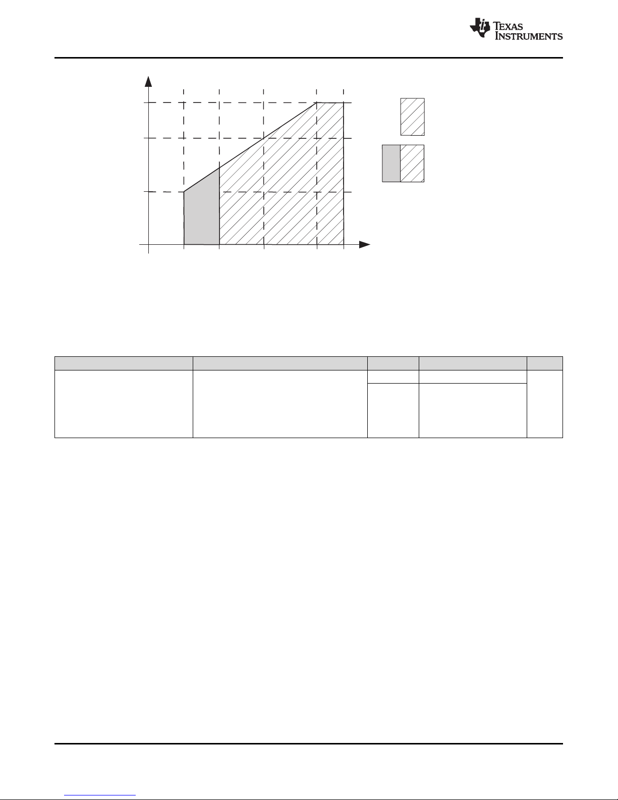
1.8 V
Supply Voltage - V
3.3 V
2.7 V
2.2 V
3.6 V
MSP430G2533,MSP430G2433,MSP430G2333,MSP430G2233
MSP430G2403, MSP430G2303, MSP430G2203
SLAS734G –APRIL 2011–REVISED APRIL 2016
www.ti.com
Note: Minimum processor frequency is defined by system clock. Flash program or erase operations require a minimum V
of 2.2 V.
CC
Figure 5-1. Safe Operating Area
5.4 Active Mode Supply Current Into VCCExcluding External Current
over recommended ranges of supply voltage and operating free-air temperature (unless otherwise noted)
I
AM,1MHz
PARAMETER TEST CONDITIONS V
f
= f
Active mode (AM)
current at 1 MHz
MCLK
= 0 Hz,
= f
DCO
f
ACLK
Program executes in flash,
BCSCTL1 = CALBC1_1MHZ,
DCOCTL = CALDCO_1MHZ,
SMCLK
= 1 MHz,
CC
2.2 V 230
3 V 330 420
CPUOFF = 0, SCG0 = 0, SCG1 = 0,
OSCOFF = 0
(1) All inputs are tied to 0 V or to VCC. Outputs do not source or sink any current.
(2) The currents are characterized with a Micro Crystal CC4V-T1A SMD crystal with a load capacitance of 9 pF. The internal and external
load capacitance is chosen to closely match the required 9 pF.
MIN TYP MAX UNIT
(1)(2)
µA
14
Specifications Copyright © 2011–2016, Texas Instruments Incorporated
Product Folder Links: MSP430G2533 MSP430G2433 MSP430G2333 MSP430G2233 MSP430G2403 MSP430G2303
Submit Documentation Feedback
MSP430G2203

0.0
1.0
2.0
3.0
4.0
5.0
1.5 2.0 2.5 3.0 3.5 4.0
VCC− Supply Voltage − V
Active Mode Current − mA
f
DCO
= 1 MHz
f
DCO
= 8 MHz
f
DCO
= 12 MHz
f
DCO
= 16 MHz
0.0
1.0
2.0
3.0
4.0
0.0 4.0 8.0 12.0 16.0
f
DCO
− DCO Frequency − MHz
Active Mode Current − mA
TA= 25 °C
TA= 85 °C
VCC= 2.2 V
VCC= 3 V
TA= 25 °C
TA= 85 °C
MSP430G2533,MSP430G2433,MSP430G2333,MSP430G2233
MSP430G2403, MSP430G2303, MSP430G2203
www.ti.com
SLAS734G –APRIL 2011–REVISED APRIL 2016
5.5 Typical Characteristics, Active Mode Supply Current (Into VCC)
Figure 5-2. Active Mode Current vs VCC, TA= 25°C Figure 5-3. Active Mode Current vs DCO Frequency
Product Folder Links: MSP430G2533 MSP430G2433 MSP430G2333 MSP430G2233 MSP430G2403 MSP430G2303
Submit Documentation Feedback
MSP430G2203
SpecificationsCopyright © 2011–2016, Texas Instruments Incorporated
15

MSP430G2533,MSP430G2433,MSP430G2333,MSP430G2233
MSP430G2403, MSP430G2303, MSP430G2203
SLAS734G –APRIL 2011–REVISED APRIL 2016
www.ti.com
5.6 Low-Power Mode Supply Currents (Into VCC) Excluding External Current
over recommended ranges of supply voltage and operating free-air temperature (unless otherwise noted)
I
LPM0,1MHz
PARAMETER TEST CONDITIONS T
f
= 0 MHz,
MCLK
f
= f
= 1 MHz,
DCO
= 32768 Hz,
Low-power mode 0
(LPM0) current
(3)
SMCLK
f
ACLK
BCSCTL1 = CALBC1_1MHZ,
DCOCTL = CALDCO_1MHZ,
A
25°C 2.2 V 56 µA
CPUOFF = 1, SCG0 = 0, SCG1 = 0,
OSCOFF = 0
f
I
LPM2
Low-power mode 2
(LPM2) current
(4)
= f
MCLK
f
= 1 MHz,
DCO
f
= 32768 Hz,
ACLK
BCSCTL1 = CALBC1_1MHZ,
DCOCTL = CALDCO_1MHZ,
SMCLK
= 0 MHz,
25°C 2.2 V 22 µA
CPUOFF = 1, SCG0 = 0, SCG1 = 1,
OSCOFF = 0
f
= f
I
LPM3,LFXT1
Low-power mode 3
(LPM3) current
(4)
DCO
f
ACLK
CPUOFF = 1, SCG0 = 1, SCG1 = 1,
= f
MCLK
= 32768 Hz,
SMCLK
= 0 MHz,
25°C 2.2 V 0.7 1.5 µA
OSCOFF = 0
f
= f
I
LPM3,VLO
Low-power mode 3
current, (LPM3)
(4)
DCO
f
ACLK
CPUOFF = 1, SCG0 = 1, SCG1 = 1,
= f
MCLK
from internal LF oscillator (VLO),
SMCLK
= 0 MHz,
25°C 2.2 V 0.5 0.7 µA
OSCOFF = 0
f
= f
I
LPM4
Low-power mode 4
(LPM4) current
(5)
MCLK
= 0 Hz,
= f
DCO
f
ACLK
CPUOFF = 1, SCG0 = 1, SCG1 = 1,
OSCOFF = 1
SMCLK
= 0 MHz,
25°C
85°C 0.8 1.7
(1) All inputs are tied to 0 V or to VCC. Outputs do not source or sink any current.
(2) The currents are characterized with a Micro Crystal CC4V-T1A SMD crystal with a load capacitance of 9 pF. The internal and external
load capacitance is chosen to closely match the required 9 pF.
(3) Current for brownout and WDT clocked by SMCLK included.
(4) Current for brownout and WDT clocked by ACLK included.
(5) Current for brownout included.
V
CC
2.2 V
(1) (2)
MIN TYP MAX UNIT
0.1 0.5
µA
16
Specifications Copyright © 2011–2016, Texas Instruments Incorporated
Product Folder Links: MSP430G2533 MSP430G2433 MSP430G2333 MSP430G2233 MSP430G2403 MSP430G2303
Submit Documentation Feedback
MSP430G2203

0.00
0.25
0.50
0.75
1.00
1.25
1.50
1.75
2.00
2.25
2.50
2.75
3.00
-40
I – Low-Power Mode Current – µA
LPM3
V = 3.6 V
CC
T – Temperature – °C
A
VCC= 1.8 V
VCC= 3 V
VCC= 2.2 V
-20
0
20
40 60 80
0.00
0.25
0.50
0.75
1.00
1.25
1.50
1.75
2.00
2.25
2.50
-40
I – Low-Power Mode Current – µA
LPM4
V = 3.6 V
CC
T – Temperature – °C
A
VCC= 1.8 V
VCC= 3 V
VCC= 2.2 V
-20
0
20
40 60 80
MSP430G2533,MSP430G2433,MSP430G2333,MSP430G2233
MSP430G2403, MSP430G2303, MSP430G2203
www.ti.com
SLAS734G –APRIL 2011–REVISED APRIL 2016
5.7 Typical Characteristics, Low-Power Mode Supply Currents
over recommended ranges of supply voltage and operating free-air temperature (unless otherwise noted)
Figure 5-4. LPM3 Current vs Temperature
Product Folder Links: MSP430G2533 MSP430G2433 MSP430G2333 MSP430G2233 MSP430G2403 MSP430G2303
Figure 5-5. LPM4 Current vs Temperature
Submit Documentation Feedback
MSP430G2203
SpecificationsCopyright © 2011–2016, Texas Instruments Incorporated
17

MSP430G2533,MSP430G2433,MSP430G2333,MSP430G2233
MSP430G2403, MSP430G2303, MSP430G2203
SLAS734G –APRIL 2011–REVISED APRIL 2016
www.ti.com
5.8 Thermal Resistance Characteristics
PARAMETER VALUE
VQFN (RHB-32) 32.1
Rθ
JA
Junction-to-ambient thermal resistance, still air
(2)
TSSOP (PW-28) 72.2
TSSOP (PW-20) 86.5
PDIP (N-20) 49.3
VQFN (RHB-32) 22.3
Rθ
JC(TOP)
Junction-to-case (top) thermal resistance
(3)
TSSOP (PW-28) 18.3
TSSOP (PW-20) 20.8
PDIP (N-20) 41
VQFN (RHB-32) 1.4
Rθ
JC(BOTTOM)
Junction-to-case (bottom) thermal resistance
TSSOP (PW-28) N/A
TSSOP (PW-20) N/A
PDIP (N-20) N/A
VQFN (RHB-32) 6.1
θ
JB
Junction-to-board thermal resistance
(4)
TSSOP (PW-28) 30.4
TSSOP (PW-20) 39
PDIP (N-20) 30.2
VQFN (RHB-32) 0.3
Ψ
JT
Junction-to-package-top characterization parameter
TSSOP (PW-28) 0.7
TSSOP (PW-20) 0.8
PDIP (N-20) 18.1
VQFN (RHB-32) 6.1
Ψ
JB
Junction-to-board characterization parameter
TSSOP (PW-28) 29.9
TSSOP (PW-20) 38.1
PDIP (N-20) 30.1
(1) These values are based on a JEDEC-defined 2S2P system (with the exception of the Theta JC (RθJC) value, which is based on a
JEDEC-defined 1S0P system) and will change based on environment and application. For more information, see these EIA/JEDEC
standards:
• JESD51-2, Integrated Circuits Thermal Test Method Environmental Conditions - Natural Convection (Still Air)
• JESD51-3, Low Effective Thermal Conductivity Test Board for Leaded Surface Mount Packages
• JESD51-7, High Effective Thermal Conductivity Test Board for Leaded Surface Mount Packages
• JESD51-9, Test Boards for Area Array Surface Mount Package Thermal Measurements
(2) The junction-to-ambient thermal resistance under natural convection is obtained in a simulation on a JEDEC-standard, High-K board, as
specified in JESD51-7, in an environment described in JESD51-2a.
(3) The junction-to-case (top) thermal resistance is obtained by simulating a cold plate test on the package top. No specific JEDEC-
standard test exists, but a close description can be found in the ANSI SEMI standard G30-88.
(4) The junction-to-board thermal resistance is obtained by simulating in an environment with a ring cold plate fixture to control the PCB
temperature, as described in JESD51-8.
(1)
UNIT
°C/W
°C/W
°C/W
°C/W
°C/W
°C/W
18
Specifications Copyright © 2011–2016, Texas Instruments Incorporated
Product Folder Links: MSP430G2533 MSP430G2433 MSP430G2333 MSP430G2233 MSP430G2403 MSP430G2303
Submit Documentation Feedback
MSP430G2203

MSP430G2533,MSP430G2433,MSP430G2333,MSP430G2233
MSP430G2403, MSP430G2303, MSP430G2203
www.ti.com
SLAS734G –APRIL 2011–REVISED APRIL 2016
5.9 Schmitt-Trigger Inputs, Ports Px
over recommended ranges of supply voltage and operating free-air temperature (unless otherwise noted)
PARAMETER TEST CONDITIONS V
V
Positive-going input threshold voltage
IT+
V
Negative-going input threshold voltage
IT–
V
Input voltage hysteresis (V
hys
R
Pullup or pulldown resistor
Pull
C
Input capacitance VIN= VSSor V
I
IT+
– V
) 3 V 0.3 1 V
IT–
For pullup: VIN= V
For pulldown: VIN= V
SS
CC
CC
CC
3 V 1.35 2.25
3 V 0.75 1.65
3 V 20 35 50 kΩ
MIN TYP MAX UNIT
0.45 V
0.25 V
CC
CC
0.75 V
0.55 V
5 pF
CC
CC
5.10 Leakage Current, Ports Px
over recommended ranges of supply voltage and operating free-air temperature (unless otherwise noted)
I
lkg(Px.y)
PARAMETER TEST CONDITIONS V
High-impedance leakage current See
(1) (2)
CC
3 V ±50 nA
(1) The leakage current is measured with VSSor VCCapplied to the corresponding pins, unless otherwise noted.
(2) The leakage of the digital port pins is measured individually. The port pin is selected for input and the pullup/pulldown resistor is
disabled.
MIN MAX UNIT
V
V
5.11 Outputs, Ports Px
over recommended ranges of supply voltage and operating free-air temperature (unless otherwise noted)
PARAMETER TEST CONDITIONS V
V
V
High-level output voltage I
OH
Low-level output voltage I
OL
(1) The maximum total current, I
specified.
(OHmax)
and I
= –6 mA
(OHmax)
= 6 mA
(OLmax)
, for all outputs combined should not exceed ±48 mA to hold the maximum voltage drop
(OLmax)
(1)
(1)
CC
3 V VCC– 0.3 V
3 V VSS+ 0.3 V
MIN TYP MAX UNIT
5.12 Output Frequency, Ports Px
over recommended ranges of supply voltage and operating free-air temperature (unless otherwise noted)
f
Px.y
f
Port_CLK
PARAMETER TEST CONDITIONS V
Port output frequency (with load) Px.y, CL= 20 pF, RL= 1 kΩ
Clock output frequency Px.y, CL= 20 pF
(2)
(1) (2)
CC
3 V 12 MHz
3 V 16 MHz
(1) A resistive divider with two 50-kΩ resistors between VCCand VSSis used as load. The output is connected to the center tap of the
divider.
(2) The output voltage reaches at least 10% and 90% VCCat the specified toggle frequency.
MIN TYP MAX UNIT
Product Folder Links: MSP430G2533 MSP430G2433 MSP430G2333 MSP430G2233 MSP430G2403 MSP430G2303
Submit Documentation Feedback
MSP430G2203
SpecificationsCopyright © 2011–2016, Texas Instruments Incorporated
19

VOH− High-Level Output Voltage − V
−25
−20
−15
−10
−5
0
0 0.5 1 1.5 2 2.5
VCC= 2.2 V
P1.7
TA= 25°C
TA= 85°C
OH
I − Typical High-Level Output Current − mA
VOH− High-Level Output Voltage − V
−50
−40
−30
−20
−10
0
0 0.5 1 1.5 2 2.5 3 3.5
VCC= 3 V
P1.7
TA= 25°C
TA= 85°C
OH
I − Typical High-Level Output Current − mA
VOL− Low-Level Output Voltage − V
0
5
10
15
20
25
30
0 0.5 1 1.5 2 2.5
VCC= 2.2 V
P1.7
TA= 25°C
TA= 85°C
OL
I − Typical Low-Level Output Current − mA
VOL− Low-Level Output Voltage − V
0
10
20
30
40
50
0 0.5 1 1.5 2 2.5 3 3.5
VCC= 3 V
P1.7
TA= 25°C
TA= 85°C
OL
I − Typical Low-Level Output Current − mA
MSP430G2533,MSP430G2433,MSP430G2333,MSP430G2233
MSP430G2403, MSP430G2303, MSP430G2203
SLAS734G –APRIL 2011–REVISED APRIL 2016
5.13 Typical Characteristics – Outputs
over recommended ranges of supply voltage and operating free-air temperature (unless otherwise noted)
www.ti.com
Figure 5-6. Typical Low-Level Output Current vs Low-Level
Figure 5-8. Typical High-Level Output Current vs High-Level
Output Voltage
Output Voltage
Figure 5-7. Typical Low-Level Output Current vs Low-Level
Figure 5-9. Typical High-Level Output Current vs High-Level
Output Voltage
Output Voltage
20
Specifications Copyright © 2011–2016, Texas Instruments Incorporated
Product Folder Links: MSP430G2533 MSP430G2433 MSP430G2333 MSP430G2233 MSP430G2403 MSP430G2303
Submit Documentation Feedback
MSP430G2203

C − External Capacitance − pF
LOAD
0.00
0.15
0.30
0.45
0.60
0.75
0.90
1.05
1.20
1.35
1.50
10 50 100
P1.y
P2.0 to P2.5
P2.6, P2.7
V = 3.0 V
CC
f − Typical Oscillation Frequency − MHz
osc
C − External Capacitance − pF
LOAD
0.00
0.15
0.30
0.45
0.60
0.75
0.90
1.05
1.20
1.35
1.50
10 50 100
P1.y
P2.0 to P2.5
P2.6, P2.7
V = 2.2 V
CC
f − Typical Oscillation Frequency − MHz
osc
MSP430G2533,MSP430G2433,MSP430G2333,MSP430G2233
MSP430G2403, MSP430G2303, MSP430G2203
www.ti.com
SLAS734G –APRIL 2011–REVISED APRIL 2016
5.14 Pin-Oscillator Frequency – Ports Px
over recommended ranges of supply voltage and operating free-air temperature (unless otherwise noted)
PARAMETER TEST CONDITIONS V
fo
fo
fo
fo
Port output oscillation frequency
P1.x
Port output oscillation frequency
P2.x
Port output oscillation frequency
P2.6/7
Port output oscillation frequency
P3.x
P1.y, CL= 10 pF, RL= 100 kΩ
P1.y, CL= 20 pF, RL= 100 kΩ
P2.0 to P2.5, CL= 10 pF, RL= 100 kΩ
P2.0 to P2.5, CL= 20 pF, RL= 100 kΩ
P2.6 and P2.7, CL= 20 pF, RL= 100
(1)(2)
kΩ
P3.y, CL= 10 pF, RL= 100 kΩ
P3.y, CL= 20 pF, RL= 100 kΩ
(1)(2)
(1)(2)
(1)(2)
(1)(2)
(1)(2)
(1)(2)
3 V
3 V
3 V 700 kHz
3 V
(1) A resistive divider with two 50-kΩ resistors between VCCand VSSis used as load. The output is connected to the center tap of the
divider.
(2) The output voltage reaches at least 10% and 90% VCCat the specified toggle frequency.
MIN TYP MAX UNIT
CC
1400
900
1800
1000
1800
1000
5.15 Typical Characteristics – Pin-Oscillator Frequency
kHz
kHz
kHz
Figure 5-10. Typical Oscillating Frequency vs Load Capacitance
Product Folder Links: MSP430G2533 MSP430G2433 MSP430G2333 MSP430G2233 MSP430G2403 MSP430G2303
One output active at a time.
Figure 5-11. Typical Oscillating Frequency vs Load Capacitance
Submit Documentation Feedback
MSP430G2203
One output active at a time.
SpecificationsCopyright © 2011–2016, Texas Instruments Incorporated
21

V
CC(drop)
V
CC
3 V
t
pw
0
0.5
1
1.5
2
0.001 1 1000
Typical Conditions
1 ns 1 ns
tpw− Pulse Width − µs
V
CC(drop)
− V
tpw− Pulse Width − µs
VCC= 3 V
0
1
t
d(BOR)
V
CC
V
(B_IT−)
V
hys(B_IT−)
V
CC(s tar t)
MSP430G2533,MSP430G2433,MSP430G2333,MSP430G2233
MSP430G2403, MSP430G2303, MSP430G2203
SLAS734G –APRIL 2011–REVISED APRIL 2016
www.ti.com
5.16 POR, BOR
(1)(2)
over recommended ranges of supply voltage and operating free-air temperature (unless otherwise noted)
PARAMETER
V
CC(start)
V
(B_IT–)
V
hys(B_IT–)
t
d(BOR)
t
(reset)
See Figure 5-12 dVCC/dt ≤ 3 V/s 0.7 V
See Figure 5-12 through Figure 5-14 dVCC/dt ≤ 3 V/s 1.35 V
See Figure 5-12 dVCC/dt ≤ 3 V/s 140 mV
See Figure 5-12 2000 µs
Pulse duration needed at RST/NMI pin to accepted
reset internally
(1) The current consumption of the brownout module is already included in the ICCcurrent consumption data. The voltage level V
V
hys(B_IT–)
(2) During power up, the CPU begins code execution following a period of t
must not be changed until VCC≥ V
is ≤ 1.8 V.
CC(min)
, where V
is the minimum supply voltage for the desired operating frequency.
CC(min)
TEST
CONDITIONS
d(BOR)
V
CC
MIN TYP MAX UNIT
(B_IT--)
2.2 V 2 µs
after VCC= V
(B_IT–)
+ V
. The default DCO settings
hys(B_IT–)
(B_IT–)
V
+
Figure 5-12. POR and BOR vs Supply Voltage
Figure 5-13. V
CC(drop)
Level With a Square Voltage Drop to Generate a POR or BOR Signal
22
Specifications Copyright © 2011–2016, Texas Instruments Incorporated
Product Folder Links: MSP430G2533 MSP430G2433 MSP430G2333 MSP430G2233 MSP430G2403 MSP430G2303
Submit Documentation Feedback
MSP430G2203

V
CC
0
0.5
1
1.5
2
V
CC(drop)
t
pw
tpw− Pulse Width − µs
V
CC(drop)
− V
3 V
0.001 1 1000
t
f
t
r
tpw− Pulse Width − µs
tf= t
r
Typical Conditions
VCC= 3 V
www.ti.com
MSP430G2533,MSP430G2433,MSP430G2333,MSP430G2233
MSP430G2403, MSP430G2303, MSP430G2203
SLAS734G –APRIL 2011–REVISED APRIL 2016
Figure 5-14. V
CC(drop)
Level With a Triangle Voltage Drop to Generate a POR or BOR Signal
Product Folder Links: MSP430G2533 MSP430G2433 MSP430G2333 MSP430G2233 MSP430G2403 MSP430G2303
Submit Documentation Feedback
MSP430G2203
SpecificationsCopyright © 2011–2016, Texas Instruments Incorporated
23

DCO(RSEL,DCO+1)
DCO(RSEL,DCO)
average
DCO(RSEL,DCO) DCO(RSEL,DCO+1)
32 × f × f
f =
MOD × f + (32 – MOD) × f
MSP430G2533,MSP430G2433,MSP430G2333,MSP430G2233
MSP430G2403, MSP430G2303, MSP430G2203
SLAS734G –APRIL 2011–REVISED APRIL 2016
5.17 Main DCO Characteristics
• All ranges selected by RSELx overlap with RSELx + 1: RSELx = 0 overlaps RSELx = 1, ... RSELx = 14 overlaps RSELx = 15.
• DCO control bits DCOx have a step size as defined by parameter S
• Modulation control bits MODx select how often f
f
DCO(RSEL,DCO)
is used for the remaining cycles. The frequency is an average equal to:
DCO(RSEL,DCO+1)
.
DCO
is used within the period of 32 DCOCLK cycles. The frequency
5.18 DCO Frequency
over recommended ranges of supply voltage and operating free-air temperature (unless otherwise noted)
PARAMETER TEST CONDITIONS V
CC
RSELx < 14 1.8 3.6
V
CC
Supply voltage
RSELx = 15 3 3.6
f
DCO(0,0)
f
DCO(0,3)
f
DCO(1,3)
f
DCO(2,3)
f
DCO(3,3)
f
DCO(4,3)
f
DCO(5,3)
f
DCO(6,3)
f
DCO(7,3)
f
DCO(8,3)
f
DCO(9,3)
f
DCO(10,3)
f
DCO(11,3)
f
DCO(12,3)
f
DCO(13,3)
f
DCO(14,3)
f
DCO(15,3)
f
DCO(15,7)
S
RSEL
S
DCO
DCO frequency (0, 0) RSELx = 0, DCOx = 0, MODx = 0 3 V 0.06 0.14 MHz
DCO frequency (0, 3) RSELx = 0, DCOx = 3, MODx = 0 3 V 0.07 0.17 MHz
DCO frequency (1, 3) RSELx = 1, DCOx = 3, MODx = 0 3 V 0.15 MHz
DCO frequency (2, 3) RSELx = 2, DCOx = 3, MODx = 0 3 V 0.21 MHz
DCO frequency (3, 3) RSELx = 3, DCOx = 3, MODx = 0 3 V 0.30 MHz
DCO frequency (4, 3) RSELx = 4, DCOx = 3, MODx = 0 3 V 0.41 MHz
DCO frequency (5, 3) RSELx = 5, DCOx = 3, MODx = 0 3 V 0.58 MHz
DCO frequency (6, 3) RSELx = 6, DCOx = 3, MODx = 0 3 V 0.54 1.06 MHz
DCO frequency (7, 3) RSELx = 7, DCOx = 3, MODx = 0 3 V 0.80 1.50 MHz
DCO frequency (8, 3) RSELx = 8, DCOx = 3, MODx = 0 3 V 1.6 MHz
DCO frequency (9, 3) RSELx = 9, DCOx = 3, MODx = 0 3 V 2.3 MHz
DCO frequency (10, 3) RSELx = 10, DCOx = 3, MODx = 0 3 V 3.4 MHz
DCO frequency (11, 3) RSELx = 11, DCOx = 3, MODx = 0 3 V 4.25 MHz
DCO frequency (12, 3) RSELx = 12, DCOx = 3, MODx = 0 3 V 4.30 7.30 MHz
DCO frequency (13, 3) RSELx = 13, DCOx = 3, MODx = 0 3 V 6.00 9.60 MHz
DCO frequency (14, 3) RSELx = 14, DCOx = 3, MODx = 0 3 V 8.60 13.9 MHz
DCO frequency (15, 3) RSELx = 15, DCOx = 3, MODx = 0 3 V 12.0 18.5 MHz
DCO frequency (15, 7) RSELx = 15, DCOx = 7, MODx = 0 3 V 16.0 26.0 MHz
Frequency step between
range RSEL and RSEL+1
Frequency step between
tap DCO and DCO+1
S
S
= f
RSEL
DCO(RSEL+1,DCO)/fDCO(RSEL,DCO)
= f
DCO
DCO(RSEL,DCO+1)/fDCO(RSEL,DCO)
3 V 1.35 ratio
3 V 1.08 ratio
Duty cycle Measured at SMCLK output 3 V 50%
MIN TYP MAX UNIT
www.ti.com
VRSELx = 14 2.2 3.6
24
Specifications Copyright © 2011–2016, Texas Instruments Incorporated
Product Folder Links: MSP430G2533 MSP430G2433 MSP430G2333 MSP430G2233 MSP430G2403 MSP430G2303
Submit Documentation Feedback
MSP430G2203

MSP430G2533,MSP430G2433,MSP430G2333,MSP430G2233
MSP430G2403, MSP430G2303, MSP430G2203
www.ti.com
SLAS734G –APRIL 2011–REVISED APRIL 2016
5.19 Calibrated DCO Frequencies, Tolerance
over recommended ranges of supply voltage and operating free-air temperature (unless otherwise noted)
PARAMETER TEST CONDITIONS T
1-MHz tolerance over
temperature
(1)
BCSCTL1 = CALBC1_1MHZ,
DCOCTL = CALDCO_1MHZ,
calibrated at 30°C and 3 V
A
0°C to 85°C 3 V –3% ±0.5% +3%
BCSCTL1 = CALBC1_1MHZ,
1-MHz tolerance over V
CC
DCOCTL = CALDCO_1MHZ,
calibrated at 30°C and 3 V
30°C 1.8 V to 3.6 V –3% ±2% +3%
BCSCTL1 = CALBC1_1MHZ,
1-MHz tolerance overall
DCOCTL = CALDCO_1MHZ,
–40°C to 85°C 1.8 V to 3.6 V –6% ±3% +6%
calibrated at 30°C and 3 V
8-MHz tolerance over
temperature
(1)
BCSCTL1 = CALBC1_8MHZ,
DCOCTL = CALDCO_8MHZ,
calibrated at 30°C and 3 V
0°C to 85°C 3 V –3% ±0.5% +3%
BCSCTL1 = CALBC1_8MHZ,
8-MHz tolerance over V
CC
DCOCTL = CALDCO_8MHZ,
calibrated at 30°C and 3 V
30°C 2.2 V to 3.6 V –3% ±2% +3%
BCSCTL1 = CALBC1_8MHZ,
8-MHz tolerance overall
DCOCTL = CALDCO_8MHZ,
–40°C to 85°C 2.2 V to 3.6 V –6% ±3% +6%
calibrated at 30°C and 3 V
12-MHz tolerance over
temperature
(1)
BCSCTL1 = CALBC1_12MHZ,
DCOCTL = CALDCO_12MHZ,
calibrated at 30°C and 3 V
0°C to 85°C 3 V –3% ±0.5% +3%
BCSCTL1 = CALBC1_12MHZ,
12-MHz tolerance over V
CC
DCOCTL = CALDCO_12MHZ,
calibrated at 30°C and 3 V
30°C 2.7 V to 3.6 V –3% ±2% +3%
BCSCTL1 = CALBC1_12MHZ,
12-MHz tolerance overall
DCOCTL = CALDCO_12MHZ,
–40°C to 85°C 2.7 V to 3.6 V –6% ±3% +6%
calibrated at 30°C and 3 V
16-MHz tolerance over
temperature
(1)
BCSCTL1 = CALBC1_16MHZ,
DCOCTL = CALDCO_16MHZ,
calibrated at 30°C and 3 V
0°C to 85°C 3 V –3% ±0.5% +3%
BCSCTL1 = CALBC1_16MHZ,
16-MHz tolerance over V
CC
DCOCTL = CALDCO_16MHZ,
calibrated at 30°C and 3 V
30°C 3.3 V to 3.6 V –3% ±2% +3%
BCSCTL1 = CALBC1_16MHZ,
16-MHz tolerance overall
DCOCTL = CALDCO_16MHZ,
–40°C to 85°C 3.3 V to 3.6 V –6% ±3% +6%
calibrated at 30°C and 3 V
(1) This is the frequency change from the measured frequency at 30°C over temperature.
V
CC
MIN TYP MAX UNIT
Product Folder Links: MSP430G2533 MSP430G2433 MSP430G2333 MSP430G2233 MSP430G2403 MSP430G2303
Submit Documentation Feedback
MSP430G2203
SpecificationsCopyright © 2011–2016, Texas Instruments Incorporated
25

DCO Frequency − MHz
0.10
1.00
10.00
0.10 1.00 10.00
DCO Wake Time − µs
RSELx = 0...11
RSELx = 12...15
MSP430G2533,MSP430G2433,MSP430G2333,MSP430G2233
MSP430G2403, MSP430G2303, MSP430G2203
SLAS734G –APRIL 2011–REVISED APRIL 2016
www.ti.com
5.20 Wake-up Times From Lower-Power Modes (LPM3, LPM4)
over recommended ranges of supply voltage and operating free-air temperature (unless otherwise noted)
t
DCO,LPM3/4
t
CPU,LPM3/4
PARAMETER TEST CONDITIONS V
DCO clock wake-up time from LPM3 or
(1)
LPM4
CPU wake-up time from LPM3 or
(2)
LPM4
BCSCTL1 = CALBC1_1MHz,
DCOCTL = CALDCO_1MHz
CC
3 V 1.5 µs
(1) The DCO clock wake-up time is measured from the edge of an external wake-up signal (for example, port interrupt) to the first clock
edge observable externally on a clock pin (MCLK or SMCLK).
(2) Parameter applicable only if DCOCLK is used for MCLK.
MIN TYP MAX UNIT
1/f
+
MCLK
t
Clock,LPM3/4
5.21 Typical Characteristics, DCO Clock Wake-up Time From LPM3 or LPM4
Figure 5-15. DCO Wake-up Time From LPM3 vs DCO Frequency
26
Specifications Copyright © 2011–2016, Texas Instruments Incorporated
Product Folder Links: MSP430G2533 MSP430G2433 MSP430G2333 MSP430G2233 MSP430G2403 MSP430G2303
Submit Documentation Feedback
MSP430G2203

www.ti.com
MSP430G2533,MSP430G2433,MSP430G2333,MSP430G2233
MSP430G2403, MSP430G2303, MSP430G2203
SLAS734G –APRIL 2011–REVISED APRIL 2016
5.22 Crystal Oscillator, XT1, Low-Frequency Mode
(1)
over recommended ranges of supply voltage and operating free-air temperature (unless otherwise noted)
f
LFXT1,LF
PARAMETER TEST CONDITIONS V
LFXT1 oscillator crystal
frequency, LF mode 0, 1
XTS = 0, LFXT1Sx = 0 or 1 1.8 V to 3.6 V 32768 Hz
CC
LFXT1 oscillator logic level
f
LFXT1,LF,logic
square-wave input frequency,
LF mode
XTS = 0, XCAPx = 0, LFXT1Sx = 3 1.8 V to 3.6 V 10000 32768 50000 Hz
XTS = 0, LFXT1Sx = 0,
OA
LF
Oscillation allowance for
LF crystals
f
XTS = 0, LFXT1Sx = 0,
f
LFXT1,LF
LFXT1,LF
= 32768 Hz, C
= 32768 Hz, C
L,eff
L,eff
= 6 pF
= 12 pF
XTS = 0, XCAPx = 0 1
C
L,eff
Integrated effective load
capacitance, LF mode
(2)
XTS = 0, XCAPx = 1 5.5
XTS = 0, XCAPx = 2 8.5
XTS = 0, XCAPx = 3 11
XTS = 0, Measured at P2.0/ACLK,
f
LFXT1,LF
= 32768 Hz
XTS = 0, XCAPx = 0, LFXT1Sx = 3
2.2 V 30% 50% 70%
(4)
2.2 V 10 10000 Hz
f
Fault,LF
Duty cycle, LF mode
Oscillator fault frequency,
LF mode
(3)
(1) To improve EMI on the XT1 oscillator, the following guidelines should be observed.
• Keep the trace between the device and the crystal as short as possible.
• Design a good ground plane around the oscillator pins.
• Prevent crosstalk from other clock or data lines into oscillator pins XIN and XOUT.
• Avoid running PCB traces underneath or adjacent to the XIN and XOUT pins.
• Use assembly materials and processes that avoid any parasitic load on the oscillator XIN and XOUT pins.
• If conformal coating is used, make sure that it does not induce capacitive or resistive leakage between the oscillator pins.
• Do not route the XOUT line to the JTAG header to support the serial programming adapter as shown in other documentation. This
signal is no longer required for the serial programming adapter.
(2) Includes parasitic bond and package capacitance (approximately 2 pF per pin).
Because the PCB adds additional capacitance, verify the correct load by measuring the ACLK frequency. For a correct setup, the
effective load capacitance should always match the specification of the used crystal.
(3) Frequencies below the MIN specification set the fault flag. Frequencies above the MAX specification do not set the fault flag.
Frequencies in between might set the flag.
(4) Measured with logic-level input frequency but also applies to operation with crystals.
MIN TYP MAX UNIT
500
200
kΩ
pF
5.23 Internal Very-Low-Power Low-Frequency Oscillator (VLO)
over recommended ranges of supply voltage and operating free-air temperature (unless otherwise noted)
PARAMETER T
f
VLO
df
VLO/dT
df
VLO
VLO frequency –40°C to 85°C 3 V 4 12 20 kHz
VLO frequency temperature drift –40°C to 85°C 3 V 0.5 %/°C
/dVCCVLO frequency supply voltage drift 25°C 1.8 V to 3.6 V 4 %/V
5.24 Timer_A
over recommended ranges of supply voltage and operating free-air temperature (unless otherwise noted)
PARAMETER TEST CONDITIONS V
f
TA
t
TA,cap
Timer_A input clock frequency SMCLK, duty cycle = 50% ±10% f
Timer_A capture timing TA0, TA1 3 V 20 ns
Product Folder Links: MSP430G2533 MSP430G2433 MSP430G2333 MSP430G2233 MSP430G2403 MSP430G2303
A
Submit Documentation Feedback
MSP430G2203
V
CC
CC
MIN TYP MAX UNIT
MIN TYP MAX UNIT
SYSTEM
MHz
SpecificationsCopyright © 2011–2016, Texas Instruments Incorporated
27

t
SU,MI
t
HD,MI
UCLK
SOMI
SIMO
t
VALID,MO
CKPL = 0
CKPL = 1
1/f
UCxCLK
t
HD,MO
t
LO/HI
t
LO/HI
t
SU,MI
t
HD,MI
UCLK
SOMI
SIMO
t
VALID,MO
t
HD,MO
CKPL = 0
CKPL = 1
t
LO/HI
t
LO/HI
1/f
UCxCLK
MSP430G2533,MSP430G2433,MSP430G2333,MSP430G2233
MSP430G2403, MSP430G2303, MSP430G2203
SLAS734G –APRIL 2011–REVISED APRIL 2016
www.ti.com
5.25 USCI (UART Mode)
over recommended ranges of supply voltage and operating free-air temperature (unless otherwise noted)
PARAMETER TEST CONDITIONS V
f
USCI
f
max,BITCLK
t
τ
USCI input clock frequency SMCLK, duty cycle = 50% ±10% f
Maximum BITCLK clock frequency
(equals baud rate in MBaud)
UART receive deglitch time
(1)
(2)
3 V 2 MHz
3 V 50 100 600 ns
(1) The DCO wake-up time must be considered in LPM3 and LPM4 for baud rates above 1 MHz.
(2) Pulses on the UART receive input (UCxRX) shorter than the UART receive deglitch time are suppressed. To ensure that pulses are
correctly recognized, their duration should exceed the maximum specification of the deglitch time.
MIN TYP MAX UNIT
CC
SYSTEM
MHz
5.26 USCI (SPI Master Mode)
over recommended ranges of supply voltage and operating free-air temperature (unless otherwise noted) (see Figure 5-16
and Figure 5-17)
f
USCI
t
SU,MI
t
HD,MI
t
VALID,MO
PARAMETER TEST CONDITIONS V
CC
USCI input clock frequency SMCLK, duty cycle = 50% ±10% f
SOMI input data setup time 3 V 75 ns
SOMI input data hold time 3 V 0 ns
SIMO output data valid time UCLK edge to SIMO valid, CL= 20 pF 3 V 20 ns
MIN MAX UNIT
SYSTEM
MHz
28
Specifications Copyright © 2011–2016, Texas Instruments Incorporated
Product Folder Links: MSP430G2533 MSP430G2433 MSP430G2333 MSP430G2233 MSP430G2403 MSP430G2303
Figure 5-16. SPI Master Mode, CKPH = 0
Figure 5-17. SPI Master Mode, CKPH = 1
Submit Documentation Feedback
MSP430G2203
STE
UCLK
CKPL = 0
CKPL = 1
SOMI
SIMO
t
SU,SI
t
HD,SI
t
VALID,SO
t
STE,LEAD
1/f
UCxCLK
t
STE,LAG
t
STE,DIS
t
STE,ACC
t
HD,MO
t
LO/HI
t
LO/HI
STE
UCLK
CKPL = 0
CKPL = 1
SOMI
SIMO
t
SU,SI
t
HD,SI
t
VALID,SO
t
STE,LEAD
1/f
UCxCLK
t
LO/HI
t
LO/HI
t
STE,LAG
t
STE,DIS
t
STE,ACC
t
HD,SO
MSP430G2533,MSP430G2433,MSP430G2333,MSP430G2233
MSP430G2403, MSP430G2303, MSP430G2203
www.ti.com
SLAS734G –APRIL 2011–REVISED APRIL 2016
5.27 USCI (SPI Slave Mode)
over recommended ranges of supply voltage and operating free-air temperature (unless otherwise noted) (see Figure 5-18
and Figure 5-19)
t
STE,LEAD
t
STE,LAG
t
STE,ACC
t
STE,DIS
t
SU,SI
t
HD,SI
t
VALID,SO
PARAMETER TEST CONDITIONS V
CC
STE lead time, STE low to clock 3 V 50 ns
STE lag time, Last clock to STE high 3 V 10 ns
STE access time, STE low to SOMI data out 3 V 50 ns
STE disable time, STE high to SOMI high
impedance
3 V 50 ns
SIMO input data setup time 3 V 15 ns
SIMO input data hold time 3 V 10 ns
SOMI output data valid time
UCLK edge to SOMI valid,
CL= 20 pF
3 V 50 75 ns
MIN TYP MAX UNIT
Product Folder Links: MSP430G2533 MSP430G2433 MSP430G2333 MSP430G2233 MSP430G2403 MSP430G2303
Figure 5-18. SPI Slave Mode, CKPH = 0
Figure 5-19. SPI Slave Mode, CKPH = 1
Submit Documentation Feedback
MSP430G2203
SpecificationsCopyright © 2011–2016, Texas Instruments Incorporated
29
SDA
SCL
t
HD,DAT
t
SU,DAT
t
HD,STA
t
HIGH
t
LOW
t
BUF
t
HD,STA
t
SU,STA
t
SP
t
SU,STO
MSP430G2533,MSP430G2433,MSP430G2333,MSP430G2233
MSP430G2403, MSP430G2303, MSP430G2203
SLAS734G –APRIL 2011–REVISED APRIL 2016
www.ti.com
5.28 USCI (I2C Mode)
over recommended ranges of supply voltage and operating free-air temperature (unless otherwise noted) (see Figure 5-20)
f
USCI
f
SCL
t
HD,STA
t
SU,STA
t
HD,DAT
t
SU,DAT
t
SU,STO
t
SP
PARAMETER TEST CONDITIONS V
CC
USCI input clock frequency SMCLK, duty cycle = 50% ±10% f
SCL clock frequency 3 V 0 400 kHz
f
≤ 100 kHz
Hold time (repeated) START
Setup time for a repeated START
SCL
f
> 100 kHz 0.6
SCL
f
≤ 100 kHz
SCL
f
> 100 kHz 0.6
SCL
3 V
3 V
Data hold time 3 V 0 ns
Data setup time 3 V 250 ns
Setup time for STOP 3 V 4.0 µs
Pulse duration of spikes suppressed by
input filter
3 V 50 100 600 ns
MIN TYP MAX UNIT
SYSTEM
MHz
4.0
4.7
µs
µs
Figure 5-20. I2C Mode Timing
Specifications Copyright © 2011–2016, Texas Instruments Incorporated
30
Product Folder Links: MSP430G2533 MSP430G2433 MSP430G2333 MSP430G2233 MSP430G2403 MSP430G2303
Submit Documentation Feedback
MSP430G2203
MSP430G2533,MSP430G2433,MSP430G2333,MSP430G2233
MSP430G2403, MSP430G2303, MSP430G2203
www.ti.com
SLAS734G –APRIL 2011–REVISED APRIL 2016
5.29 10-Bit ADC, Power Supply and Input Range Conditions (MSP430G2x33 Only)
over recommended ranges of supply voltage and operating free-air temperature (unless otherwise noted)
V
CC
V
Ax
I
ADC10
PARAMETER TEST CONDITIONS T
Analog supply voltage VSS= 0 V 2.2 3.6 V
Analog input voltage
ADC10 supply current
(2)
(3)
All Ax terminals, Analog inputs
selected in ADC10AE register
f
ADC10CLK
ADC10ON = 1, REFON = 0,
= 5.0 MHz,
ADC10SHT0 = 1, ADC10SHT1 = 0,
A
25°C 3 V 0.6 mA
ADC10DIV = 0
I
REF+
Reference supply current,
reference buffer disabled
f
ADC10CLK
ADC10ON = 0, REF2_5V = 0,
(4)
REFON = 1, REFOUT = 0
f
ADC10CLK
ADC10ON = 0, REF2_5V = 1,
= 5.0 MHz,
= 5.0 MHz,
25°C 3 V
REFON = 1, REFOUT = 0
I
REFB,0
Reference buffer supply current
with ADC10SR = 0
(4)
f
ADC10CLK
ADC10ON = 0, REFON = 1,
REF2_5V = 0, REFOUT = 1,
= 5.0 MHz,
25°C 3 V 1.1 mA
ADC10SR = 0
I
REFB,1
Reference buffer supply current
with ADC10SR = 1
(4)
f
ADC10CLK
ADC10ON = 0, REFON = 1,
REF2_5V = 0, REFOUT = 1,
= 5.0 MHz,
25°C 3 V 0.5 mA
ADC10SR = 1
C
R
Input capacitance
I
Input MUX ON resistance 0 V ≤ VAx≤ V
I
Only one terminal Ax can be selected
at one time
CC
25°C 3 V 27 pF
25°C 3 V 1000 Ω
(1) The leakage current is defined in the leakage current table with Px.y/Ax parameter.
(2) The analog input voltage range must be within the selected reference voltage range VR+to VR–for valid conversion results.
(3) The internal reference supply current is not included in current consumption parameter I
(4) The internal reference current is supplied through terminal VCC. Consumption is independent of the ADC10ON control bit, unless a
conversion is active. The REFON bit enables the built-in reference to settle before starting an A/D conversion.
V
CC
3 V 0 V
.
ADC10
(1)
MIN TYP MAX UNIT
CC
0.25
0.25
V
mA
Product Folder Links: MSP430G2533 MSP430G2433 MSP430G2333 MSP430G2233 MSP430G2403 MSP430G2303
Submit Documentation Feedback
MSP430G2203
SpecificationsCopyright © 2011–2016, Texas Instruments Incorporated
31

MSP430G2533,MSP430G2433,MSP430G2333,MSP430G2233
MSP430G2403, MSP430G2303, MSP430G2203
SLAS734G –APRIL 2011–REVISED APRIL 2016
5.30 10-Bit ADC, Built-In Voltage Reference (MSP430G2x33 Only)
over recommended ranges of supply voltage and operating free-air temperature (unless otherwise noted)
V
CC,REF+
V
REF+
I
LD,VREF+
C
VREF+
TC
REF+
t
REFON
t
REFBURST
PARAMETER TEST CONDITIONS V
I
≤ 1 mA, REF2_5V = 0 2.2
Positive built-in reference
analog supply voltage range
Positive built-in reference
voltage
VREF+
I
≤ 1 mA, REF2_5V = 1 2.9
VREF+
I
≤ I
VREF+
I
VREF+
max, REF2_5V = 0
VREF+
≤ I
max, REF2_5V = 1 2.35 2.5 2.65
VREF+
CC
3 V
Maximum VREF+ load current 3 V ±1 mA
I
= 500 µA ±100 µA,
VREF+
Analog input voltage VAx≈ 0.75 V,
VREF+ load regulation
REF2_5V = 0
I
= 500 µA ±100 µA,
VREF+
Analog input voltage VAx≈ 1.25 V,
3 V
REF2_5V = 1
I
= 100 µA → 900 µA,
V
load regulation response
REF+
time
VREF+
VAx≈ 0.5 × VREF+,
Error of conversion result ≤ 1 LSB,
3 V 400 ns
ADC10SR = 0
Maximum capacitance at pin
VREF+
Temperature coefficient I
Settling time of internal
reference voltage to 99.9%
VREF
Settling time of reference buffer
to 99.9% VREF
I
≤ ±1 mA, REFON = 1, REFOUT = 1 3 V 100 pF
VREF+
= const with 0 mA ≤ I
VREF+
I
= 0.5 mA, REF2_5V = 0,
VREF+
REFON = 0 → 1
I
= 0.5 mA,
VREF+
REF2_5V = 1, REFON = 1,
≤ 1 mA 3 V ±100
VREF+
3.6 V 30 µs
3 V 2 µs
REFBURST = 1, ADC10SR = 0
MIN TYP MAX UNIT
1.41 1.5 1.59
www.ti.com
V
V
±2
LSB
±2
ppm/
°C
32
Specifications Copyright © 2011–2016, Texas Instruments Incorporated
Product Folder Links: MSP430G2533 MSP430G2433 MSP430G2333 MSP430G2233 MSP430G2403 MSP430G2303
Submit Documentation Feedback
MSP430G2203

www.ti.com
MSP430G2533,MSP430G2433,MSP430G2333,MSP430G2233
MSP430G2403, MSP430G2303, MSP430G2203
SLAS734G –APRIL 2011–REVISED APRIL 2016
5.31 10-Bit ADC, External Reference
(1)
(MSP430G2x33 Only)
over recommended ranges of supply voltage and operating free-air temperature (unless otherwise noted)
PARAMETER TEST CONDITIONS V
CC
VEREF+ > VEREF–,
VEREF+
VEREF–
ΔVEREF
Positive external reference input
voltage range
Negative external reference input
voltage range
(2)
(4)
Differential external reference input
voltage range,
SREF1 = 1, SREF0 = 0
VEREF– ≤ VEREF+ ≤ VCC– 0.15 V,
SREF1 = 1, SREF0 = 1
(3)
VEREF+ > VEREF– 0 1.2 V
VEREF+ > VEREF–
(5)
ΔVEREF = VEREF+ – VEREF–
I
VEREF+
I
VEREF–
0 V ≤ VEREF+ ≤ VCC,
Static input current into VEREF+
SREF1 = 1, SREF0 = 0
0 V ≤ VEREF+ ≤ VCC– 0.15 V ≤ 3 V,
SREF1 = 1, SREF0 = 1
Static input current into VEREF– 0 V ≤ VEREF– ≤ V
(3)
CC
3 V ±1
3 V 0
3 V ±1 µA
(1) The external reference is used during conversion to charge and discharge the capacitance array. The input capacitance, CI, is also the
dynamic load for an external reference during conversion. The dynamic impedance of the reference supply should follow the
recommendations on analog-source impedance to allow the charge to settle for 10-bit accuracy.
(2) The accuracy limits the minimum positive external reference voltage. Lower reference voltage levels may be applied with reduced
accuracy requirements.
(3) Under this condition, the external reference is internally buffered. The reference buffer is active and requires the reference buffer supply
current I
(4) The accuracy limits the maximum negative external reference voltage. Higher reference voltage levels may be applied with reduced
. The current consumption can be limited to the sample and conversion period with REBURST = 1.
REFB
accuracy requirements.
(5) The accuracy limits the minimum external differential reference voltage. Lower differential reference voltage levels may be applied with
reduced accuracy requirements.
MIN TYP MAX UNIT
1.4 V
CC
V
1.4 3
1.4 V
CC
V
µA
5.32 10-Bit ADC, Timing Parameters (MSP430G2x33 Only)
over recommended ranges of supply voltage and operating free-air temperature (unless otherwise noted)
PARAMETER TEST CONDITIONS V
f
ADC10CLK
f
ADC10OSC
ADC10 input clock
frequency
ADC10 built-in
oscillator frequency
For specified performance of
ADC10 linearity parameters
ADC10DIVx = 0, ADC10SSELx = 0,
f
ADC10CLK
= f
ADC10OSC
ADC10 built-in oscillator, ADC10SSELx = 0,
t
CONVERT
t
ADC10ON
Conversion time
Turnon settling time
of the ADC
f
ADC10CLK
f
ADC10CLK
ADC10SSELx ≠ 0
(1)
= f
ADC10OSC
from ACLK, MCLK, or SMCLK:
(1) The condition is that the error in a conversion started after t
settled.
CC
ADC10SR = 0
ADC10SR = 1 0.45 1.5
3 V
3 V 3.7 6.3 MHz
3 V 2.06 3.51
ADC10ON
is less than ±0.5 LSB. The reference and input signal are already
MIN TYP MAX UNIT
0.45 6.3
13 ×
ADC10DIV ×
1 / f
ADC10CLK
5.33 10-Bit ADC, Linearity Parameters (MSP430G2x33 Only)
over recommended ranges of supply voltage and operating free-air temperature (unless otherwise noted)
PARAMETER TEST CONDITIONS V
E
Integral linearity error 3 V ±1 LSB
I
E
Differential linearity error 3 V ±1 LSB
D
E
Offset error Source impedance RS< 100 Ω 3 V ±1 LSB
O
E
Gain error 3 V ±1.1 ±2 LSB
G
E
Total unadjusted error 3 V ±2 ±5 LSB
T
CC
MIN TYP MAX UNIT
MHz
µs
100 ns
Product Folder Links: MSP430G2533 MSP430G2433 MSP430G2333 MSP430G2233 MSP430G2403 MSP430G2303
Submit Documentation Feedback
MSP430G2203
SpecificationsCopyright © 2011–2016, Texas Instruments Incorporated
33

MSP430G2533,MSP430G2433,MSP430G2333,MSP430G2233
MSP430G2403, MSP430G2303, MSP430G2203
SLAS734G –APRIL 2011–REVISED APRIL 2016
www.ti.com
5.34 10-Bit ADC, Temperature Sensor and Built-In V
(MSP430G2x33 Only)
MID
over recommended ranges of supply voltage and operating free-air temperature (unless otherwise noted)
PARAMETER TEST CONDITIONS V
I
SENSOR
TC
SENSOR
t
Sensor(sample)
I
VMID
V
MID
t
VMID(sample)
Temperature sensor supply
current
Sample time required if channel 10
is selected
Current into divider at channel 11 ADC10ON = 1, INCHx = 0Bh 3 V
VCCdivider at channel 11
Sample time required if channel 11
is selected
(1) The sensor current I
high). When REFON = 1, I
input (INCH = 0Ah).
(1)
SENSOR
REFON = 0, INCHx = 0Ah, TA= 25°C 3 V 60 µA
ADC10ON = 1, INCHx = 0Ah
(3)
ADC10ON = 1, INCHx = 0Ah,
Error of conversion result ≤ 1 LSB
(2)
ADC10ON = 1, INCHx = 0Bh,
V
≈ 0.5 × V
MID
(5)
ADC10ON = 1, INCHx = 0Bh,
Error of conversion result ≤ 1 LSB
CC
is consumed if (ADC10ON = 1 and REFON = 1) or (ADC10ON = 1 and INCH = 0Ah and sample signal is
SENSOR
is included in I
. When REFON = 0, I
REF+
applies during conversion of the temperature sensor
SENSOR
CC
3 V 3.55 mV/°C
3 V 30 µs
3 V 1.5 V
3 V 1220 ns
(2) The following formula can be used to calculate the temperature sensor output voltage:
V
Sensor,typ
V
Sensor,typ
(3) The typical equivalent impedance of the sensor is 51 kΩ. The sample time required includes the sensor-on time t
(4) No additional current is needed. The V
(5) The on-time t
= TC
= TC
(273 + T [°C] ) + V
Sensor
T [°C] + V
Sensor
is included in the sampling time t
VMID(on)
Sensor(TA
Offset,sensor
= 0°C) [mV]
MID
[mV] or
is used during sampling.
VMID(sample)
; no additional on time is needed.
MIN TYP MAX UNIT
(4)
µA
SENSOR(on)
.
5.35 Flash Memory
over recommended ranges of supply voltage and operating free-air temperature (unless otherwise noted)
PARAMETER
V
CC(PGM/ERASE)
f
FTG
I
PGM
I
ERASE
t
CPT
t
CMErase
Program and erase supply voltage 2.2 3.6 V
Flash timing generator frequency 257 476 kHz
Supply current from VCCduring program 2.2 V, 3.6 V 1 5 mA
Supply current from VCCduring erase 2.2 V, 3.6 V 1 7 mA
Cumulative program time
(1)
Cumulative mass erase time 2.2 V, 3.6 V 20 ms
Program and erase endurance 10
t
Retention
t
Word
t
Block, 0
t
Block, 1-63
t
Block, End
t
Mass Erase
t
Seg Erase
Data retention duration TJ= 25°C 100 years
Word or byte program time See
Block program time for first byte or word See
Block program time for each additional byte or
word
Block program end-sequence wait time See
Mass erase time See
Segment erase time See
(1) Do not exceed the cumulative program time when writing to a 64-byte flash block. This parameter applies to all programming methods:
individual word or byte write and block write modes.
(2) These values are hardwired into the state machine of the flash controller (t
TEST
CONDITIONS
(2)
(2)
(2)
See
(2)
(2)
(2)
FTG
V
CC
MIN TYP MAX UNIT
2.2 V, 3.6 V 10 ms
4
5
10
30 t
25 t
18 t
6 t
10593 t
4819 t
= 1/f
).
FTG
cycles
FTG
FTG
FTG
FTG
FTG
FTG
34
Specifications Copyright © 2011–2016, Texas Instruments Incorporated
Product Folder Links: MSP430G2533 MSP430G2433 MSP430G2333 MSP430G2233 MSP430G2403 MSP430G2303
Submit Documentation Feedback
MSP430G2203

MSP430G2533,MSP430G2433,MSP430G2333,MSP430G2233
MSP430G2403, MSP430G2303, MSP430G2203
www.ti.com
SLAS734G –APRIL 2011–REVISED APRIL 2016
5.36 RAM
over recommended ranges of supply voltage and operating free-air temperature (unless otherwise noted)
PARAMETER TEST CONDITIONS MIN MAX UNIT
V
RAM retention supply voltage
(RAMh)
(1) This parameter defines the minimum supply voltage VCCwhen the data in RAM remains unchanged. No program execution should
happen during this supply voltage condition.
(1)
CPU halted 1.6 V
5.37 JTAG and Spy-Bi-Wire Interface
over recommended ranges of supply voltage and operating free-air temperature (unless otherwise noted)
PARAMETER V
f
SBW
t
SBW,Low
t
SBW,En
t
SBW,Ret
f
TCK
R
Internal
Spy-Bi-Wire input frequency 2.2 V 0 20 MHz
Spy-Bi-Wire low clock pulse duration 2.2 V 0.025 15 µs
Spy-Bi-Wire enable time
(TEST high to acceptance of first clock edge
(1)
)
Spy-Bi-Wire return to normal operation time 2.2 V 15 100 µs
TCK input frequency
(2)
Internal pulldown resistance on TEST 2.2 V 25 60 90 kΩ
(1) Tools that access the Spy-Bi-Wire interface must wait for the maximum t
applying the first SBWCLK clock edge.
(2) f
5.38 JTAG Fuse
may be restricted to meet the timing requirements of the module selected.
TCK
(1)
time after pulling the TEST/SBWCLK pin high before
SBW,En
CC
2.2 V 1 µs
2.2 V 0 5 MHz
over recommended ranges of supply voltage and operating free-air temperature (unless otherwise noted)
PARAMETER TEST CONDITIONS MIN MAX UNIT
V
CC(FB)
V
FB
I
FB
t
FB
Supply voltage during fuse-blow condition TA= 25°C 2.5 V
Voltage level on TEST for fuse blow 6 7 V
Supply current into TEST during fuse blow 100 mA
Time to blow fuse 1 ms
MIN TYP MAX UNIT
(1) After the fuse is blown, no further access to the JTAG/Test, Spy-Bi-Wire, and emulation features is possible, and JTAG is switched to
bypass mode.
Product Folder Links: MSP430G2533 MSP430G2433 MSP430G2333 MSP430G2233 MSP430G2403 MSP430G2303
Submit Documentation Feedback
MSP430G2203
SpecificationsCopyright © 2011–2016, Texas Instruments Incorporated
35

Program Counter
PC/R0
Stack Pointer SP/R1
Status Register
SR/CG1/R2
Constant Generator CG2/R3
General-Purpose Register
R4
General-Purpose Register
R5
General-Purpose Register
R6
General-Purpose Register
R7
General-Purpose Register
R8
General-Purpose Register
R9
General-Purpose Register
R10
General-Purpose Register
R11
General-Purpose Register
R12
General-Purpose Register
R13
General-Purpose Register
R15
General-Purpose Register
R14
MSP430G2533,MSP430G2433,MSP430G2333,MSP430G2233
MSP430G2403, MSP430G2303, MSP430G2203
SLAS734G –APRIL 2011–REVISED APRIL 2016
6 Detailed Description
6.1 CPU
The MSP430 CPU has a 16-bit RISC architecture that is highly transparent to the application. All
operations, other than program-flow instructions, are performed as register operations in conjunction with
seven addressing modes for source operand and four addressing modes for destination operand.
The CPU is integrated with 16 registers that provide reduced instruction execution time. The register-toregister operation execution time is one cycle of the CPU clock. Four of the registers, R0 to R3, are
dedicated as program counter, stack pointer, status register, and constant generator, respectively. The
remaining registers are general-purpose registers (see Figure 6-1).
Peripherals are connected to the CPU using data, address, and control buses, and can be handled with all
instructions.
The instruction set consists of the original 51 instructions with three formats and seven address modes
and additional instructions for the expanded address range. Each instruction can operate on word and
byte data.
www.ti.com
36
Detailed Description Copyright © 2011–2016, Texas Instruments Incorporated
Product Folder Links: MSP430G2533 MSP430G2433 MSP430G2333 MSP430G2233 MSP430G2403 MSP430G2303
Figure 6-1. Integrated CPU Registers
Submit Documentation Feedback
MSP430G2203

MSP430G2533,MSP430G2433,MSP430G2333,MSP430G2233
MSP430G2403, MSP430G2303, MSP430G2203
www.ti.com
SLAS734G –APRIL 2011–REVISED APRIL 2016
6.2 Instruction Set
The instruction set consists of 51 instructions with three formats and seven address modes. Each
instruction can operate on word and byte data. Table 6-1 lists examples of the three types of instruction
formats. Table 6-2 lists the address modes.
Table 6-1. Instruction Word Formats
INSTRUCTION FORMAT EXAMPLE OPERATION
Dual operands, source-destination ADD R4,R5 R4 + R5 → R5
Single operands, destination only CALL R8 PC → (TOS), R8 → PC
Relative jump, unconditional or conditional JNE Jump-on-equal bit = 0
Table 6-2. Address Mode Descriptions
ADDRESS MODE S
Register ✓ ✓ MOV Rs,Rd MOV R10,R11 R10 → R11
Indexed ✓ ✓ MOV X(Rn),Y(Rm) MOV 2(R5),6(R6) M(2+R5) → M(6+R6)
Symbolic (PC relative) ✓ ✓ MOV EDE,TONI M(EDE) → M(TONI)
Absolute ✓ ✓ MOV &MEM,&TCDAT M(MEM) → M(TCDAT)
Indirect ✓ MOV @Rn,Y(Rm) MOV @R10,Tab(R6) M(R10) → M(Tab+R6)
Indirect autoincrement ✓ MOV @Rn+,Rm MOV @R10+,R11
Immediate ✓ MOV #X,TONI MOV #45,TONI #45 → M(TONI)
(1) S = source, D = destination
(1)
D SYNTAX EXAMPLE OPERATION
M(R10) → R11
R10 + 2 → R10
Product Folder Links: MSP430G2533 MSP430G2433 MSP430G2333 MSP430G2233 MSP430G2403 MSP430G2303
Submit Documentation Feedback
MSP430G2203
Detailed DescriptionCopyright © 2011–2016, Texas Instruments Incorporated
37

MSP430G2533,MSP430G2433,MSP430G2333,MSP430G2233
MSP430G2403, MSP430G2303, MSP430G2203
SLAS734G –APRIL 2011–REVISED APRIL 2016
6.3 Operating Modes
These microcontrollers have one active mode and five software-selectable low-power modes of operation.
An interrupt event can wake the device from any of the low-power modes, service the request, and restore
back to the low-power mode on return from the interrupt program.
Software can configure the following operating modes:
• Active mode (AM)
– All clocks are active
• Low-power mode 0 (LPM0)
– CPU is disabled
– ACLK and SMCLK remain active, MCLK is disabled
• Low-power mode 1 (LPM1)
– CPU is disabled
– ACLK and SMCLK remain active, MCLK is disabled
– DC generator of the DCO is disabled if DCO not used in active mode
• Low-power mode 2 (LPM2)
– CPU is disabled
– MCLK and SMCLK are disabled
– DC generator of the DCO remains enabled
– ACLK remains active
• Low-power mode 3 (LPM3)
– CPU is disabled
– MCLK and SMCLK are disabled
– DC generator of the DCO is disabled
– ACLK remains active
• Low-power mode 4 (LPM4)
– CPU is disabled
– ACLK is disabled
– MCLK and SMCLK are disabled
– DC generator of the DCO is disabled
– Crystal oscillator is stopped
www.ti.com
38
Detailed Description Copyright © 2011–2016, Texas Instruments Incorporated
Product Folder Links: MSP430G2533 MSP430G2433 MSP430G2333 MSP430G2233 MSP430G2403 MSP430G2303
Submit Documentation Feedback
MSP430G2203

www.ti.com
6.4 Interrupt Vector Addresses
The interrupt vectors and the power-up starting address are in the address range 0FFFFh to 0FFC0h (see
Table 6-3). The vector contains the 16-bit address of the appropriate interrupt handler instruction
sequence.
If the reset vector (at address 0FFFEh) contains 0FFFFh (for example, if the flash is not programmed), the
CPU goes into LPM4 immediately after power-up.
Table 6-3. Interrupt Sources, Flags, and Vectors
MSP430G2533,MSP430G2433,MSP430G2333,MSP430G2233
MSP430G2403, MSP430G2303, MSP430G2203
SLAS734G –APRIL 2011–REVISED APRIL 2016
INTERRUPT SOURCE INTERRUPT FLAG
Power up
External reset
Watchdog Timer+
Flash key violation
PC out of range
(1)
NMI
Oscillator fault
Flash memory access violation
PORIFG
RSTIFG
WDTIFG
KEYV
NMIIFG
OFIFG
ACCVIFG
Timer1_A3 TACCR0 CCIFG
Timer1_A3 TACCR2 TACCR1 CCIFG, TAIFG
SYSTEM
INTERRUPT
Reset 0FFFEh 31, highest
(2)
(non)-maskable
(2)(4)
(non)-maskable
(non)-maskable
maskable 0FFFAh 29
maskable 0FFF8h 28
(2)
(4)
(3)
WORD
ADDRESS
PRIORITY
0FFFCh 30
0FFF6h 27
Watchdog Timer+ WDTIFG maskable 0FFF4h 26
Timer0_A3 TACCR0 CCIFG
Timer0_A3
USCI_A0, USCI_B0 receive
USCI_B0 I2C status
USCI_A0, USCI_B0 transmit
USCI_B0 I2C receive or transmit
ADC10
(MSP430G2x33 only)
TACCR2 TACCR1 CCIFG, TAIFG
(5)(4)
UCA0RXIFG, UCB0RXIFG
UCA0TXIFG, UCB0TXIFG
ADC10IFG
(4)
maskable 0FFF2h 25
maskable 0FFF0h 24
(2)(5)
(2)(6)
(4)
maskable 0FFEEh 23
maskable 0FFECh 22
maskable 0FFEAh 21
0FFE8h 20
I/O Port P2 (up to eight flags) P2IFG.0 to P2IFG.7
I/O Port P1 (up to eight flags) P1IFG.0 to P1IFG.7
(2)(4)
(2)(4)
maskable 0FFE6h 19
maskable 0FFE4h 18
0FFE2h 17
0FFE0h 16
(7)
See
See
(8)
0FFDEh 15
0FFDEh to
0FFC0h
14 to 0, lowest
(1) A reset is generated if the CPU tries to fetch instructions from within the module register memory address range (0h to 01FFh) or from
within unused address ranges.
(2) Multiple source flags
(3) (non)-maskable: the individual interrupt-enable bit can disable an interrupt event, but the general interrupt enable cannot.
(4) Interrupt flags are in the module.
(5) In SPI mode: UCB0RXIFG. In I2C mode: UCALIFG, UCNACKIFG, ICSTTIFG, UCSTPIFG.
(6) In UART or SPI mode: UCB0TXIFG. In I2C mode: UCB0RXIFG, UCB0TXIFG.
(7) This location is used as bootloader security key (BSLSKEY). A 0xAA55 at this location disables the BSL completely. A zero (0h)
disables the erasure of the flash if an invalid password is supplied.
(8) The interrupt vectors at addresses 0FFDEh to 0FFC0h are not used in this device and can be used for regular program code if
necessary.
Product Folder Links: MSP430G2533 MSP430G2433 MSP430G2333 MSP430G2233 MSP430G2403 MSP430G2303
Submit Documentation Feedback
MSP430G2203
Detailed DescriptionCopyright © 2011–2016, Texas Instruments Incorporated
39

MSP430G2533,MSP430G2433,MSP430G2333,MSP430G2233
MSP430G2403, MSP430G2303, MSP430G2203
SLAS734G –APRIL 2011–REVISED APRIL 2016
6.5 Special Function Registers (SFRs)
Most interrupt and module enable bits are collected into the lowest address space. Special function
register bits not allocated to a functional purpose are not physically present in the device. Simple software
access is provided with this arrangement.
Legend
rw Bit can be read and written.
rw-0, rw-1 Bit can be read and written. It is reset or set by PUC.
rw-(0), rw-(1) Bit can be read and written. It is reset or set by POR.
SFR bit is not present in device.
Figure 6-2. Interrupt Enable Register 1 (Address = 00h)
7 6 5 4 3 2 1 0
ACCVIE NMIIE OFIE WDTIE
rw-0 rw-0 rw-0 rw-0
Table 6-4. Interrupt Enable Register 1 Description
Bit Field Type Reset Description
5 ACCVIE RW 0h Flash access violation interrupt enable
4 NMIIE RW 0h (Non)maskable interrupt enable
1 OFIE RW 0h Oscillator fault interrupt enable
0 WDTIE RW 0h
Watchdog Timer interrupt enable. Inactive if watchdog mode is selected. Active if
Watchdog Timer is configured in interval timer mode.
www.ti.com
Figure 6-3. Interrupt Enable Register 2 (Address = 01h)
7 6 5 4 3 2 1 0
UCB0TXIE UCB0RXIE UCA0TXIE UCA0RXIE
rw-0 rw-0 rw-0 rw-0
Table 6-5. Interrupt Enable Register 2 Description
Bit Field Type Reset Description
3 UCB0TXIE RW 0h USCI_B0 transmit interrupt enable
2 UCB0RXIE RW 0h USCI_B0 receive interrupt enable
1 UCA0TXIE RW 0h USCI_A0 transmit interrupt enable
0 UCA0RXIE RW 0h USCI_A0 receive interrupt enable
Figure 6-4. Interrupt Flag Register 1 (Address = 02h)
7 6 5 4 3 2 1 0
NMIIFG RSTIFG PORIFG OFIFG WDTIFG
rw-0 rw-(0) rw-(1) rw-1 rw-(0)
Table 6-6. Interrupt Flag Register 1 Description
Bit Field Type Reset Description
4 NMIIFG RW 0h Set by the RST/NMI pin
3 RSTIFG RW 0h
2 PORIFG RW 1h Power-On Reset interrupt flag. Set on VCCpower-up.
1 OFIFG RW 1h Flag set on oscillator fault.
0 WDTIFG RW 0h
External reset interrupt flag. Set on a reset condition at RST/NMI pin in reset
mode. Reset on VCCpower-up.
Set on watchdog timer overflow (in watchdog mode) or security key violation.
Reset on VCCpower-on or a reset condition at the RST/NMI pin in reset mode.
40
Detailed Description Copyright © 2011–2016, Texas Instruments Incorporated
Product Folder Links: MSP430G2533 MSP430G2433 MSP430G2333 MSP430G2233 MSP430G2403 MSP430G2303
Submit Documentation Feedback
MSP430G2203

MSP430G2533,MSP430G2433,MSP430G2333,MSP430G2233
MSP430G2403, MSP430G2303, MSP430G2203
www.ti.com
SLAS734G –APRIL 2011–REVISED APRIL 2016
Figure 6-5. Interrupt Flag Register 2 (Address = 03h)
7 6 5 4 3 2 1 0
UCB0TXIFG UCB0RXIFG UCA0TXIFG UCA0RXIFG
rw-1 rw-0 rw-1 rw-0
Table 6-7. Interrupt Flag Register 2 Description
Bit Field Type Reset Description
3 UCB0TXIFG RW 0h USCI_B0 transmit interrupt flag
2 UCB0RXIFG RW 1h USCI_B0 receive interrupt flag
1 UCA0TXIFG RW 1h USCI_A0 transmit interrupt flag
0 UCA0RXIFG RW 0h USCI_A0 receive interrupt flag
6.6 Memory Organization
Table 6-8 summarizes the memory map.
Table 6-8. Memory Organization
MSP430G2233
MSP430G2203
Memory Size 2KB 4KB 8KB 16KB
Main: interrupt vector Flash FFFFh to FFC0h FFFFh to FFC0h FFFFh to FFC0h FFFFh to FFC0h
Main: code memory Flash FFFFh to F800h FFFFh to F000h FFFFh to E000h FFFFh to C000h
Information memory Size 256 byte 256 byte 256 byte 256 byte
Flash 010FFh to 01000h 010FFh to 01000h 010FFh to 01000h 010FFh to 01000h
RAM Size 256 byte 256 byte 512 byte 512 byte
02FFh to 0200h 02FFh to 0200h 03FFh to 0200h 03FFh to 0200h
Peripherals 16-bit 01FFh to 0100h 01FFh to 0100h 01FFh to 0100h 01FFh to 0100h
8-bit 0FFh to 010h 0FFh to 010h 0FFh to 010h 0FFh to 010h
8-bit SFR 0Fh to 00h 0Fh to 00h 0Fh to 00h 0Fh to 00h
MSP430G2333
MSP430G2303
MSP430G2433
MSP430G2403
MSP430G2533
6.7 Bootloader (BSL)
The MSP430 BSL enables users to program the flash memory or RAM using a UART serial interface.
Access to the MSP430 memory through the BSL is protected by user-defined password. For complete
description of the features of the BSL and its implementation, see the MSP430 Programming With the
Bootloader User's Guide (SLAU319). Table 6-9 lists the BSL function pins.
Table 6-9. BSL Function Pins
BSL FUNCTION
Data transmit 3 - P1.1 3 - P1.1 1 - P1.1
Data receive 7 - P1.5 7 - P1.5 5 - P1.5
20-PIN PW PACKAGE
20-PIN N PACKAGE
28-PIN PW PACKAGE 32-PIN RHB PACKAGE
Product Folder Links: MSP430G2533 MSP430G2433 MSP430G2333 MSP430G2233 MSP430G2403 MSP430G2303
Submit Documentation Feedback
MSP430G2203
Detailed DescriptionCopyright © 2011–2016, Texas Instruments Incorporated
41

MSP430G2533,MSP430G2433,MSP430G2333,MSP430G2233
MSP430G2403, MSP430G2303, MSP430G2203
SLAS734G –APRIL 2011–REVISED APRIL 2016
6.8 Flash Memory
The flash memory can be programmed through the Spy-Bi-Wire/JTAG port or in-system by the CPU. The
CPU can perform single-byte and single-word writes to the flash memory. Features of the flash memory
include:
• Flash memory has n segments of main memory and four segments of information memory (A to D) of
64 bytes each. Each segment in main memory is 512 bytes in size.
• Segments 0 to n may be erased in one step, or each segment may be individually erased.
• Segments A to D can be erased individually or as a group with segments 0 to n. Segments A to D are
also called information memory.
• Segment A contains calibration data. After reset segment A is protected against programming and
erasing. It can be unlocked but care should be taken not to erase this segment if the device-specific
calibration data is required.
6.9 Peripherals
Peripherals are connected to the CPU through data, address, and control buses. The peripherals can be
managed using all instructions. For complete module descriptions, see the MSP430x2xx Family User's
Guide (SLAU144).
6.9.1 Oscillator and System Clock
www.ti.com
The clock system is supported by the basic clock module that includes support for a 32768-Hz watch
crystal oscillator, an internal very-low-power low-frequency oscillator and an internal digitally controlled
oscillator (DCO). The basic clock module is designed to meet the requirements of both low system cost
and low power consumption. The internal DCO provides a fast turnon clock source and stabilizes in less
than 1 µs. The basic clock module provides the following clock signals:
• Auxiliary clock (ACLK), sourced either from a 32768-Hz watch crystal or the internal LF oscillator.
• Main clock (MCLK), the system clock used by the CPU.
• Sub-Main clock (SMCLK), the subsystem clock used by the peripheral modules.
The DCO settings to calibrate the DCO output frequency are stored in the information memory segment A.
42
Detailed Description Copyright © 2011–2016, Texas Instruments Incorporated
Product Folder Links: MSP430G2533 MSP430G2433 MSP430G2333 MSP430G2233 MSP430G2403 MSP430G2303
Submit Documentation Feedback
MSP430G2203

MSP430G2533,MSP430G2433,MSP430G2333,MSP430G2233
MSP430G2403, MSP430G2303, MSP430G2203
www.ti.com
6.9.2 Calibration Data Stored in Information Memory Segment A
Calibration data is stored for both the DCO and for ADC10 organized in a tag-length-value structure (see
Table 6-10 and Table 6-11).
Table 6-10. Tags Used by the ADC Calibration Tags
NAME ADDRESS VALUE DESCRIPTION
TAG_DCO_30 0x10F6 0x01 DCO frequency calibration at VCC= 3 V and TA= 30°C
TAG_ADC10_1 0x10DA 0x10 ADC10_1 calibration tag
TAG_EMPTY – 0xFE Identifier for empty memory areas
Table 6-11. Labels Used by the ADC Calibration Tags
SLAS734G –APRIL 2011–REVISED APRIL 2016
LABEL
CAL_ADC_25T85 0x0010 word INCHx = 1010b, REF2_5 = 1, TA= 85°C
CAL_ADC_25T30 0x000E word INCHx = 1010b, REF2_5 = 1, TA= 30°C
CAL_ADC_25VREF_FACTOR 0x000C word REF2_5 = 1, TA= 30°C, I
CAL_ADC_15T85 0x000A word INCHx = 1010b, REF2_5 = 0, TA= 85°C
CAL_ADC_15T30 0x0008 word INCHx = 1010b, REF2_5 = 0, TA= 30°C
CAL_ADC_15VREF_FACTOR 0x0006 word REF2_5 = 0, TA= 30°C, I
CAL_ADC_OFFSET 0x0004 word External VREF = 1.5 V, f
CAL_ADC_GAIN_FACTOR 0x0002 word External VREF = 1.5 V, f
CAL_BC1_1MHZ 0x0009 byte –
CAL_DCO_1MHZ 0x0008 byte –
CAL_BC1_8MHZ 0x0007 byte –
CAL_DCO_8MHZ 0x0006 byte –
CAL_BC1_12MHZ 0x0005 byte –
CAL_DCO_12MHZ 0x0004 byte –
CAL_BC1_16MHZ 0x0003 byte –
CAL_DCO_16MHZ 0x0002 byte –
ADDRESS
OFFSET
SIZE CONDITION AT CALIBRATION
6.9.3 Brownout
The brownout circuit is implemented to provide the proper internal reset signal to the device during power
on and power off.
VREF+
VREF+
ADC10CLK
ADC10CLK
= 1 mA
= 0.5 mA
= 5 MHz
= 5 MHz
6.9.4 Digital I/O
Up to three 8-bit I/O ports are implemented:
• All individual I/O bits are independently programmable.
• Any combination of input, output, and interrupt condition (port P1 and port P2 only) is possible.
• Edge-selectable interrupt input capability for all bits of port P1 and port P2 (if available).
• Read/write access to port-control registers is supported by all instructions.
• Each I/O has an individually programmable pullup or pulldown resistor.
• Each I/O has an individually programmable pin oscillator enable bit to enable low-cost capacitive touch
detection.
Product Folder Links: MSP430G2533 MSP430G2433 MSP430G2333 MSP430G2233 MSP430G2403 MSP430G2303
Submit Documentation Feedback
MSP430G2203
Detailed DescriptionCopyright © 2011–2016, Texas Instruments Incorporated
43

MSP430G2533,MSP430G2433,MSP430G2333,MSP430G2233
MSP430G2403, MSP430G2303, MSP430G2203
SLAS734G –APRIL 2011–REVISED APRIL 2016
6.9.5 WDT+ Watchdog Timer
The primary function of the watchdog timer (WDT+) module is to perform a controlled system restart after
a software problem occurs. If the selected time interval expires, a system reset is generated. If the
watchdog function is not needed in an application, the module can be disabled or configured as an interval
timer and can generate interrupts at selected time intervals.
6.9.6 Timer_A3 (TA0, TA1)
Timer0_A3 and Timer1_A3 are 16-bit timers/counters with three capture/compare registers. Timer_A3 can
support multiple capture/compares, PWM outputs, and interval timing (see Table 6-12 and Table 6-13).
Timer_A3 also has extensive interrupt capabilities. Interrupts may be generated from the counter on
overflow conditions and from each of the capture/compare registers.
Table 6-12. Timer0_A3 Signal Connections
www.ti.com
INPUT PIN NUMBER DEVICE
PW20, N20 PW28 RHB32 PW20, N20 PW28 RHB32
P1.0-2 P1.0-2 P1.0-31 TACLK TACLK
PinOsc PinOsc PinOsc TACLK INCLK
P1.1-3 P1.1-3 P1.1-1 TA0.0 CCI0A
P1.2-4 P1.2-4 P1.2-2 TA0.1 CCI1A
– P3.0-9 P3.0-7 TA0.2 CCI2A
PinOsc PinOsc PinOsc TA0.2 CCI2B – P3.6-20 P3.6-19
INPUT
SIGNAL
ACLK ACLK
SMCLK SMCLK
ACLK CCI0B P1.5-7 P1.5-7 P1.5-5
V
SS
V
CC
CAOUT CCI1B P1.6-14 P1.6-22 P1.6-21
V
SS
V
CC
V
SS
V
CC
MODULE
INPUT
NAME
GND – P3.4-15 P3.4-14
V
CC
GND P2.6-19 P2.6-27 P2.6-26
V
CC
GND
V
CC
MODULE
BLOCK
Timer NA
CCR0 TA0
CCR1 TA1
CCR2 TA2
MODULE
OUTPUT
SIGNAL
OUTPUT PIN NUMBER
P1.1-3 P1.1-3 P1.1-1
P1.2-4 P1.2-4 P1.2-2
– P3.5-19 P3.5-18
– P3.0-9 P3.0-7
44
Detailed Description Copyright © 2011–2016, Texas Instruments Incorporated
Product Folder Links: MSP430G2533 MSP430G2433 MSP430G2333 MSP430G2233 MSP430G2403 MSP430G2303
Submit Documentation Feedback
MSP430G2203

www.ti.com
MSP430G2533,MSP430G2433,MSP430G2333,MSP430G2233
MSP430G2403, MSP430G2303, MSP430G2203
SLAS734G –APRIL 2011–REVISED APRIL 2016
Table 6-13. Timer1_A3 Signal Connections
INPUT PIN NUMBER DEVICE
PW20, N20 PW28 RHB32 PW20, N20 PW28 RHB32
– P3.7-21 P3.7-20 TACLK TACLK
– P3.7-21 P3.7-20 TACLK INCLK
P2.0-8 P2.0-10 P2.0-9 TA1.0 CCI0A
P2.3-11 P2.3-16 P2.3-12 TA1.0 CCI0B P2.3-11 P2.3-16 P2.3-15
P2.1-9 P2.1-11 P2.1-10 TA1.1 CCI1A
P2.2-10 P2.2-12 P2.2-11 TA1.1 CCI1B P2.2-10 P2.2-12 P2.2-11
P2.4-12 P2.4-17 P2.4-16 TA1.2 CCI2A
P2.5-13 P2.5-18 P2.5-17 TA1.2 CCI2B P2.5-13 P2.5-18 P2.5-17
INPUT
SIGNAL
ACLK ACLK
SMCLK SMCLK
V
SS
V
CC
V
SS
V
CC
V
SS
V
CC
MODULE
INPUT
NAME
GND P3.1-8 P3.1-6
V
CC
GND P3.2-13 P3.2-12
V
CC
GND P3.3-14 P3.3-13
V
CC
MODULE
BLOCK
Timer NA
CCR0 TA0
CCR1 TA1
CCR2 TA2
MODULE
OUTPUT
SIGNAL
OUTPUT PIN NUMBER
P2.0-8 P2.0-10 P2.0-9
P2.1-9 P2.1-11 P2.1-10
P2.4-12 P2.4-17 P2.4-16
6.9.7 Universal Serial Communications Interface (USCI)
The USCI module is used for serial data communication. The USCI module supports synchronous
communication protocols such as SPI (3-pin or 4-pin) and I2C, and asynchronous communication
protocols such as UART, enhanced UART with automatic baud rate detection (LIN), and IrDA. Not all
packages support the USCI functionality.
USCI_A0 provides support for SPI (3-pin or 4-pin), UART, enhanced UART, and IrDA.
USCI_B0 provides support for SPI (3-pin or 4-pin) and I2C.
6.9.8 ADC10 (MSP430G2x33 Only)
The ADC10 module supports fast 10-bit analog-to-digital conversions. The module implements a 10-bit
SAR core, sample select control, reference generator, and data transfer controller (DTC) for automatic
conversion result handling, allowing ADC samples to be converted and stored without any CPU
intervention.
Product Folder Links: MSP430G2533 MSP430G2433 MSP430G2333 MSP430G2233 MSP430G2403 MSP430G2303
Submit Documentation Feedback
MSP430G2203
Detailed DescriptionCopyright © 2011–2016, Texas Instruments Incorporated
45
MSP430G2533,MSP430G2433,MSP430G2333,MSP430G2233
MSP430G2403, MSP430G2303, MSP430G2203
SLAS734G –APRIL 2011–REVISED APRIL 2016
www.ti.com
6.9.9 Peripheral File Map
Table 6-14 lists the registers that support word access. Table 6-15 that support byte access.
Table 6-14. Peripherals With Word Access
MODULE REGISTER DESCRIPTION ACRONYM OFFSET
ADC data transfer start address ADC10SA 1BCh
ADC10 (MSP430G2x33 only)
Timer1_A3
Timer0_A3
Flash Memory
Watchdog Timer+ Watchdog timer control WDTCTL 0120h
ADC memory ADC10MEM 1B4h
ADC control register 1 ADC10CTL1 1B2h
ADC control register 0 ADC10CTL0 1B0h
Capture/compare register TA1CCR2 0196h
Capture/compare register TA1CCR1 0194h
Capture/compare register TA1CCR0 0192h
Timer_A register TA1R 0190h
Capture/compare control TA1CCTL2 0186h
Capture/compare control TA1CCTL1 0184h
Capture/compare control TA1CCTL0 0182h
Timer_A control TA1CTL 0180h
Timer_A interrupt vector TA1IV 011Eh
Capture/compare register TA0CCR2 0176h
Capture/compare register TA0CCR1 0174h
Capture/compare register TA0CCR0 0172h
Timer_A register TA0R 0170h
Capture/compare control TA0CCTL2 0166h
Capture/compare control TA0CCTL1 0164h
Capture/compare control TA0CCTL0 0162h
Timer_A control TA0CTL 0160h
Timer_A interrupt vector TA0IV 012Eh
Flash control 3 FCTL3 012Ch
Flash control 2 FCTL2 012Ah
Flash control 1 FCTL1 0128h
MODULE REGISTER DESCRIPTION ACRONYM OFFSET
USCI_B0 transmit buffer UCB0TXBUF 06Fh
USCI_B0 receive buffer UCB0RXBUF 06Eh
USCI_B0 status UCB0STAT 06Dh
USCI B0 I2C Interrupt enable UCB0CIE 06Ch
USCI_B0
46
Detailed Description Copyright © 2011–2016, Texas Instruments Incorporated
Product Folder Links: MSP430G2533 MSP430G2433 MSP430G2333 MSP430G2233 MSP430G2403 MSP430G2303
USCI_B0 bit rate control 1 UCB0BR1 06Bh
USCI_B0 bit rate control 0 UCB0BR0 06Ah
USCI_B0 control 1 UCB0CTL1 069h
USCI_B0 control 0 UCB0CTL0 068h
USCI_B0 I2C slave address UCB0SA 011Ah
USCI_B0 I2C own address UCB0OA 0118h
Table 6-15. Peripherals With Byte Access
Submit Documentation Feedback
MSP430G2203
www.ti.com
MODULE REGISTER DESCRIPTION ACRONYM OFFSET
USCI_A0
ADC10 (MSP430G2x33 only)
Basic Clock System+
Port P3
(28-pin PW and 32-pin RHB only)
Port P2
Port P1
Special Function
MSP430G2533,MSP430G2433,MSP430G2333,MSP430G2233
MSP430G2403, MSP430G2303, MSP430G2203
SLAS734G –APRIL 2011–REVISED APRIL 2016
Table 6-15. Peripherals With Byte Access (continued)
USCI_A0 transmit buffer UCA0TXBUF 067h
USCI_A0 receive buffer UCA0RXBUF 066h
USCI_A0 status UCA0STAT 065h
USCI_A0 modulation control UCA0MCTL 064h
USCI_A0 baud rate control 1 UCA0BR1 063h
USCI_A0 baud rate control 0 UCA0BR0 062h
USCI_A0 control 1 UCA0CTL1 061h
USCI_A0 control 0 UCA0CTL0 060h
USCI_A0 IrDA receive control UCA0IRRCTL 05Fh
USCI_A0 IrDA transmit control UCA0IRTCTL 05Eh
USCI_A0 auto baud rate control UCA0ABCTL 05Dh
ADC analog enable 0 ADC10AE0 04Ah
ADC analog enable 1 ADC10AE1 04Bh
ADC data transfer control register 1 ADC10DTC1 049h
ADC data transfer control register 0 ADC10DTC0 048h
Basic clock system control 3 BCSCTL3 053h
Basic clock system control 2 BCSCTL2 058h
Basic clock system control 1 BCSCTL1 057h
DCO clock frequency control DCOCTL 056h
Port P3 selection 2. pin P3SEL2 043h
Port P3 resistor enable P3REN 010h
Port P3 selection P3SEL 01Bh
Port P3 direction P3DIR 01Ah
Port P3 output P3OUT 019h
Port P3 input P3IN 018h
Port P2 selection 2 P2SEL2 042h
Port P2 resistor enable P2REN 02Fh
Port P2 selection P2SEL 02Eh
Port P2 interrupt enable P2IE 02Dh
Port P2 interrupt edge select P2IES 02Ch
Port P2 interrupt flag P2IFG 02Bh
Port P2 direction P2DIR 02Ah
Port P2 output P2OUT 029h
Port P2 input P2IN 028h
Port P1 selection 2 P1SEL2 041h
Port P1 resistor enable P1REN 027h
Port P1 selection P1SEL 026h
Port P1 interrupt enable P1IE 025h
Port P1 interrupt edge select P1IES 024h
Port P1 interrupt flag P1IFG 023h
Port P1 direction P1DIR 022h
Port P1 output P1OUT 021h
Port P1 input P1IN 020h
SFR interrupt flag 2 IFG2 003h
SFR interrupt flag 1 IFG1 002h
SFR interrupt enable 2 IE2 001h
SFR interrupt enable 1 IE1 000h
Product Folder Links: MSP430G2533 MSP430G2433 MSP430G2333 MSP430G2233 MSP430G2403 MSP430G2303
Submit Documentation Feedback
MSP430G2203
Detailed DescriptionCopyright © 2011–2016, Texas Instruments Incorporated
47

PxDIR.y
From Timer
P1.0/TA0CLK/ ACLK/A0*
P1.1/TA0.0/
UCA0RXD/UCA0SOMI/A1*
P1.2/TA0.1/
UCA0TXD/UCA0SIMO/A2*
From USCI
1
* Note: MSP430G2x33 devices only. MSP430G2x03 devices have no ADC10.
To Module
From Timer
PxOUT.y
DVSS
DVCC
1
TAx.y
TAxCLK
Bus
Keeper
EN
1
0
PxIN.y
EN
D
PxSEL.y
PxREN.y
1
0
PxSEL2.y
1
0
INCHx = y *
ADC10AE0.y *
To ADC10 *
PxSEL.y
1
3
2
1
0
PxSEL2.y
PxIRQ.y
PxIE.y
EN
Set
Q
Interrupt
Edge
Select
PxSEL.y
PxIES.y
PxIFG.y
Direction
0: Input
1: Output
PxSEL.y
3
2
1
0
PxSEL2.y
0
MSP430G2533,MSP430G2433,MSP430G2333,MSP430G2233
MSP430G2403, MSP430G2303, MSP430G2203
SLAS734G –APRIL 2011–REVISED APRIL 2016
6.10 I/O Port Diagrams
6.10.1 Port P1 Pin Diagram: P1.0 to P1.2, Input/Output With Schmitt Trigger
Figure 6-6 shows the port diagram. Table 6-16 summarizes the selection of the pin functions.
www.ti.com
48
Detailed Description Copyright © 2011–2016, Texas Instruments Incorporated
Product Folder Links: MSP430G2533 MSP430G2433 MSP430G2333 MSP430G2233 MSP430G2403 MSP430G2303
Figure 6-6. Port P1 (P1.0 to P1.2) Diagram
Submit Documentation Feedback
MSP430G2203
MSP430G2533,MSP430G2433,MSP430G2333,MSP430G2233
MSP430G2403, MSP430G2303, MSP430G2203
www.ti.com
SLAS734G –APRIL 2011–REVISED APRIL 2016
Table 6-16. Port P1 (P1.0 to P1.2) Pin Functions
PIN NAME
(P1.x)
P1.0/
x FUNCTION
P1DIR.x P1SEL.x P1SEL2.x
P1.x (I/O) I: 0; O: 1 0 0 0
CONTROL BITS OR SIGNALS
TA0CLK/ TA0.TACLK 0 1 0 0
ACLK/ ACLK 1 1 0 0
(2)
A0
/ A0 X X X 1 (y = 0)
0
Pin Osc Capacitive sensing X 0 1 0
P1.1/
P1.x (I/O) I: 0; O: 1 0 0 0
TA0.0/ TA0.0 1 1 0 0
TA0.CCI0A 0 1 0 0
UCA0RXD/ UCA0RXD from USCI 1 1 0
1
UCA0SOMI/ UCA0SOMI from USCI 1 1 0
(2)
A1
/ A1 X X X 1 (y = 1)
Pin Osc Capacitive sensing X 0 1 0
P1.2/
P1.x (I/O) I: 0; O: 1 0 0 0
TA0.1/ TA0.1 1 1 0 0
TA0.CCI1A 0 1 0 0
UCA0TXD/ UCA0TXD from USCI 1 1 0
2
UCA0SIMO/ UCA0SIMO from USCI 1 1 0
(2)
A2
/ A2 X X X 1 (y = 2)
Pin Osc Capacitive sensing X 0 1 0
(1) X = don't care
(2) MSP430G2x33 devices only
(1)
ADC10AE.x
(INCH.y = 1)
(2)
Product Folder Links: MSP430G2533 MSP430G2433 MSP430G2333 MSP430G2233 MSP430G2403 MSP430G2303
Submit Documentation Feedback
MSP430G2203
Detailed DescriptionCopyright © 2011–2016, Texas Instruments Incorporated
49

* Note: MSP430G2x33 devices only. MSP430G2x03 devices have no ADC10.
P1.3/ADC10CLK*/
A3*/VREF-*/VEREF-*
Direction
0: Input
1: Output
To Module
From ADC10 *
PxOUT.y
DVSS
DVCC
1
TAx.y
TAxCLK
Bus
Keeper
EN
1
0
PxIN.y
EN
D
PxSEL.y
PxREN.y
1
0
PxDIR.y
1
0,2,3
PxSEL2.y
PxSEL.y
1
0
INCHx = y *
To ADC10 *
To ADC10 VREF- *
1
0
VSS
SREF2 *
PxSEL.y
1
3
2
1
0
PxSEL2.y
PxIRQ.y
PxIE.y
EN
Set
Q
Interrupt
Edge
Select
PxSEL.y
PxIES.y
PxIFG.y
ADC10AE0.y *
PxSEL2.y
MSP430G2533,MSP430G2433,MSP430G2333,MSP430G2233
MSP430G2403, MSP430G2303, MSP430G2203
SLAS734G –APRIL 2011–REVISED APRIL 2016
6.10.2 Port P1 Pin Diagram: P1.3, Input/Output With Schmitt Trigger
Figure 6-7 shows the port diagram. Table 6-17 summarizes the selection of the pin functions.
www.ti.com
50
Detailed Description Copyright © 2011–2016, Texas Instruments Incorporated
Product Folder Links: MSP430G2533 MSP430G2433 MSP430G2333 MSP430G2233 MSP430G2403 MSP430G2303
Figure 6-7. Port P1 (P1.3) Diagram
Submit Documentation Feedback
MSP430G2203
MSP430G2533,MSP430G2433,MSP430G2333,MSP430G2233
MSP430G2403, MSP430G2303, MSP430G2203
www.ti.com
SLAS734G –APRIL 2011–REVISED APRIL 2016
Table 6-17. Port P1 (P1.3) Pin Functions
PIN NAME
(P1.x)
P1.3/
ADC10CLK
(2)
A3
/ A3 X X X 1 (y = 3)
(2)
VREFVEREF-
/ VREF- X X X 1
(2)
/ VEREF- X X X 1
x FUNCTION
P1DIR.x P1SEL.x P1SEL2.x
P1.x (I/O) I: 0; O: 1 0 0 0
(2)
/ ADC10CLK 1 1 0 0
3
CONTROL BITS OR SIGNALS
Pin Osc Capacitive sensing X 0 1 0
(1) X = don't care
(2) MSP430G2x33 devices only
(1)
ADC10AE.x
(INCH.y = 1)
(2)
Product Folder Links: MSP430G2533 MSP430G2433 MSP430G2333 MSP430G2233 MSP430G2403 MSP430G2303
Submit Documentation Feedback
MSP430G2203
Detailed DescriptionCopyright © 2011–2016, Texas Instruments Incorporated
51

P1.4/SMCLK/UCB0STE/UCA0CLK/
VREF+/VEREF+/A4/TCK
Direction
0: Input
1: Output
To Module
SMCLK
PxOUT.y
DVSS
DVCC
1
TAx.y
TAxCLK
Bus
Keeper
EN
1
0
PxIN.y
EN
D
PxSEL.y
PxREN.y
1
0
PxDIR.y
1
0
PxSEL2.y
PxSEL.y
1
0
INCHx = y *
To ADC10 *
From/To ADC10 Ref+ *
PxSEL.y
1
3
2
1
0
PxSEL2.y
From JTAG
To JTAG
PxIRQ.y
PxIE.y
EN
Set
Q
Interrupt
Edge
Select
PxSEL.y
PxIES.y
PxIFG.y
ADC10AE0.y *
* Note: MSP430G2x33 devices only. MSP430G2x03 devices have no ADC10.
from Module
MSP430G2533,MSP430G2433,MSP430G2333,MSP430G2233
MSP430G2403, MSP430G2303, MSP430G2203
SLAS734G –APRIL 2011–REVISED APRIL 2016
6.10.3 Port P1 Pin Diagram: P1.4, Input/Output With Schmitt Trigger
www.ti.com
Figure 6-8 shows the port diagram. Table 6-18 summarizes the selection of the pin functions.
Figure 6-8. Port P1 (P1.4) Diagram
Submit Documentation Feedback
52
Detailed Description Copyright © 2011–2016, Texas Instruments Incorporated
Product Folder Links: MSP430G2533 MSP430G2433 MSP430G2333 MSP430G2233 MSP430G2403 MSP430G2303
MSP430G2203

MSP430G2533,MSP430G2433,MSP430G2333,MSP430G2233
MSP430G2403, MSP430G2303, MSP430G2203
www.ti.com
SLAS734G –APRIL 2011–REVISED APRIL 2016
Table 6-18. Port P1 (P1.4) Pin Functions
CONTROL BITS OR SIGNALS
PIN NAME
(P1.x)
P1.4/
x FUNCTION
P1DIR.x P1SEL.x P1SEL2.x
P1.x (I/O) I: 0; O: 1 0 0 0 0
SMCLK/ SMCLK 1 1 0 0 0
UCB0STE/ UCB0STE
UCA0CLK/ UCA0CLK
(2)
VREF+
VEREF+
A4
/ VREF+ X X X 1 0
(2)
(2)
/ A4 X X X 1 (y = 4) 0
4
/ VEREF+ X X X 1 0
(3)(4)
(3)(4)
from USCI 1 1 0 0
from USCI 1 1 0 0
TCK/ TCK X X X 0 1
Pin Osc Capacitive sensing X 0 1 0 0
(1) X = don't care
(2) MSP430G2x33 devices only
(3) The pin direction is controlled by the USCI module.
(4) UCA0CLK function takes precedence over UCB0STE function. If the pin is required as UCA0CLK input or output, USCI_B0 is forced to
3-wire SPI mode if 4-wire SPI mode is selected.
(1)
ADC10AE.x
(INCH.y =
(2)
1)
JTAG Mode
Product Folder Links: MSP430G2533 MSP430G2433 MSP430G2333 MSP430G2233 MSP430G2403 MSP430G2303
Submit Documentation Feedback
MSP430G2203
Detailed DescriptionCopyright © 2011–2016, Texas Instruments Incorporated
53
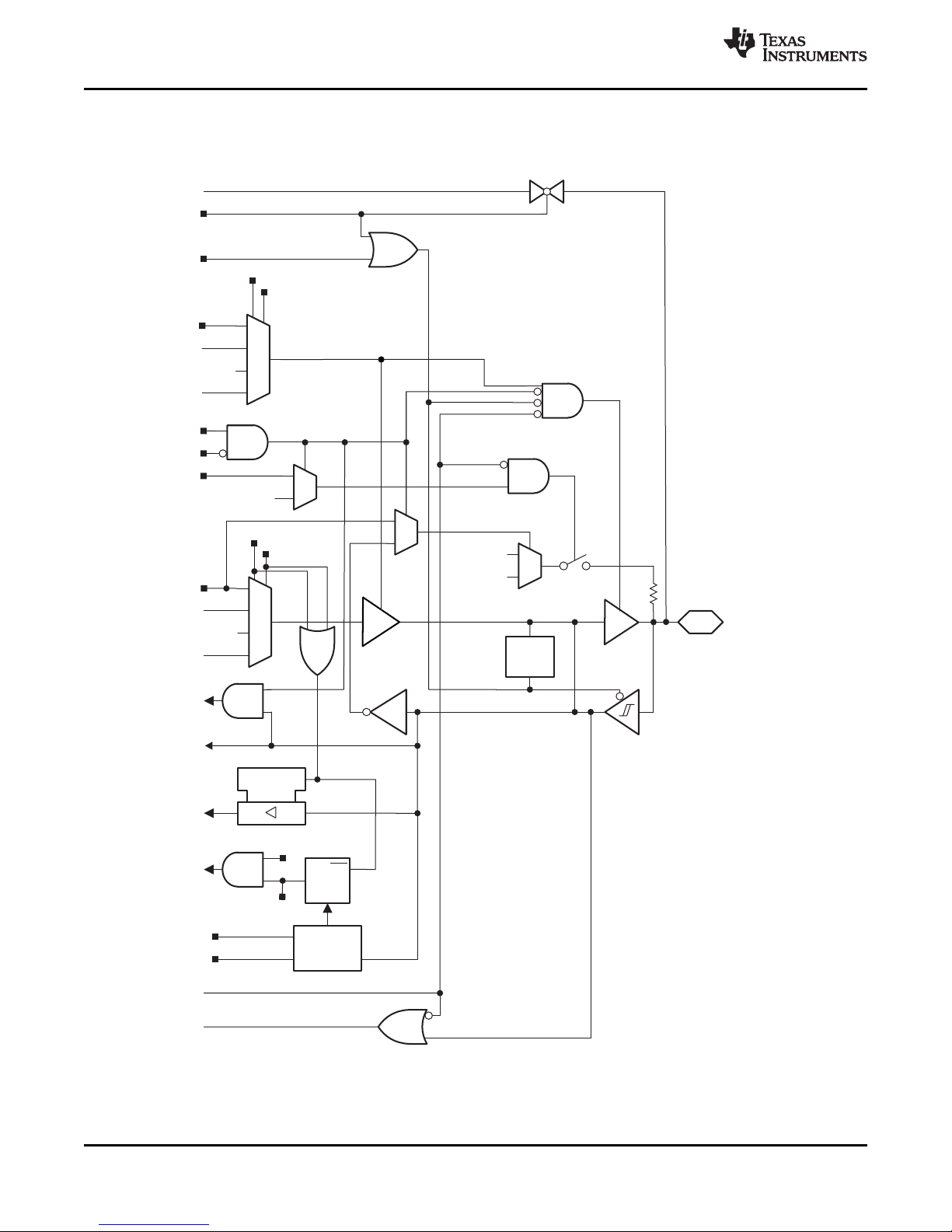
P1.5/TA0.0/UCB0CLK/
UCA0STE/A5*/TMS
P1.6/TA0.1/UCB0SOMI/
UCB0SCL/A6*/TDI/TCLK
P1.7/CAOUT/UCB0SIMO/
UCB0SDA/A7*/TDO/TDI
From Module
From Module
* Note: MSP430G2x33 devices only. MSP430G2x03 devices have no ADC10.
To Module
From Module
PxOUT.y
DV
SS
DV
CC
1
TAx.y
TAxCLK
Bus
Keeper
EN
1
0
PxIN.y
EN
D
PxSEL.y
PxREN.y
1
0
PxSEL2.y
1
0
INCHx = y *
To ADC10 *
PxSEL.y
1
3
2
1
0
PxSEL2.y
From JTAG
To JTAG
PxIRQ.y
PxIE.y
EN
Set
Q
Interrupt
Edge
Select
PxSEL.y
PxIES.y
PxIFG.y
Direction
0: Input
1: Output
PxDIR.y
From Module
PxSEL.y
3
2
1
0
PxSEL2.y
ADC10AE0.y *
MSP430G2533,MSP430G2433,MSP430G2333,MSP430G2233
MSP430G2403, MSP430G2303, MSP430G2203
SLAS734G –APRIL 2011–REVISED APRIL 2016
6.10.4 Port P1 Pin Diagram: P1.5 to P1.7, Input/Output With Schmitt Trigger
Figure 6-9 shows the port diagram. Table 6-19 summarizes the selection of the pin functions.
www.ti.com
54
Detailed Description Copyright © 2011–2016, Texas Instruments Incorporated
Product Folder Links: MSP430G2533 MSP430G2433 MSP430G2333 MSP430G2233 MSP430G2403 MSP430G2303
Figure 6-9. Port P1 (P1.5 to P1.7) Diagram
Submit Documentation Feedback
MSP430G2203

MSP430G2533,MSP430G2433,MSP430G2333,MSP430G2233
MSP430G2403, MSP430G2303, MSP430G2203
www.ti.com
SLAS734G –APRIL 2011–REVISED APRIL 2016
Table 6-19. Port P1 (P1.5 to P1.7) Pin Functions
CONTROL BITS OR SIGNALS
PIN NAME
(P1.x)
P1.5/
x FUNCTION
P1DIR.x P1SEL.x P1SEL2.x
P1.x (I/O) I: 0; O: 1 0 0 0 0
TA0.0/ TA0.0 1 1 0 0 0
UCB0CLK/ UCB0CLK
UCA0STE/ UCA0STE
(2)
A5
/ A5 X X X 1 (y = 5) 0
5
(3)(4)
(3)(4)
from USCI 1 1 0 0
from USCI 1 1 0 0
TMS TMS X X X 0 1
Pin Osc Capacitive sensing X 0 1 0 0
P1.6/
P1.x (I/O) I: 0; O: 1 0 0 0 0
TA0.1/ TA0.1 1 1 0 0 0
UCB0SOMI/ UCB0SOMI from USCI 1 1 0 0
UCB0SCL/ UCB0SCL from USCI 1 1 0 0
(2)
A6
/ A6 X X X 1 (y = 6) 0
6
TDI/TCLK/ TDI/TCLK X X X 0 1
Pin Osc Capacitive sensing X 0 1 0 0
P1.7/
P1.x (I/O) I: 0; O: 1 0 0 0 0
UCB0SIMO/ UCB0SIMO from USCI 1 1 0 0
UCB0SDA/ UCB0SDA from USCI 1 1 0 0
(2)
A7
/ A7 X X X 1 (y = 7) 0
7
TDO/TDI/ TDO/TDI X X X 0 1
Pin Osc Capacitive sensing X 0 1 0 0
(1) X = don't care
(2) MSP430G2x33 devices only
(3) The pin direction is controlled by the USCI module.
(4) UCB0CLK function takes precedence over UCA0STE function. If the pin is required as UCB0CLK input or output, USCI_A0 is forced to
3-wire SPI mode if 4-wire SPI mode is selected.
(1)
ADC10AE.x
(INCH.y =
(2)
1)
JTAG Mode
Product Folder Links: MSP430G2533 MSP430G2433 MSP430G2333 MSP430G2233 MSP430G2403 MSP430G2303
Submit Documentation Feedback
MSP430G2203
Detailed DescriptionCopyright © 2011–2016, Texas Instruments Incorporated
55

P2.0/TA1.0
P2.1/TA1.1
P2.2/TA1.1
P2.3/TA1.0
P2.4/TA1.2
P2.5/TA1.2
From Timer
Direction
0: Input
1: Output
To Module
PxOUT.y
DVSS
DVCC
1
TAx.y
TAxCLK
1
0
PxIN.y
EN
D
PxSEL.y
PxREN.y
1
0
PxSEL2.y
1
0
PxSEL.y
1
3
2
1
0
PxSEL2.y
PxIRQ.y
PxIE.y
EN
Set
Q
Interrupt
Edge
Select
PxSEL.y
PxIES.y
PxIFG.y
PxDIR.y
1
0
PxSEL.y
0
MSP430G2533,MSP430G2433,MSP430G2333,MSP430G2233
MSP430G2403, MSP430G2303, MSP430G2203
SLAS734G –APRIL 2011–REVISED APRIL 2016
6.10.5 Port P2 Pin Diagram: P2.0 to P2.5, Input/Output With Schmitt Trigger
Figure 6-10 shows the port diagram. Table 6-20 summarizes the selection of the pin functions.
www.ti.com
Figure 6-10. Port P2 (P2.0 to P2.5) Diagram
56
Detailed Description Copyright © 2011–2016, Texas Instruments Incorporated
Product Folder Links: MSP430G2533 MSP430G2433 MSP430G2333 MSP430G2233 MSP430G2403 MSP430G2303
Submit Documentation Feedback
MSP430G2203

MSP430G2533,MSP430G2433,MSP430G2333,MSP430G2233
MSP430G2403, MSP430G2303, MSP430G2203
www.ti.com
SLAS734G –APRIL 2011–REVISED APRIL 2016
Table 6-20. Port P2 (P2.0 to P2.5) Pin Functions
PIN NAME
(P2.x)
P2.0/
TA1.0/ Timer1_A3.CCI0A 0 1 0
Pin Osc Capacitive sensing X 0 1
P2.1/
TA1.1/ Timer1_A3.CCI1A 0 1 0
Pin Osc Capacitive sensing X 0 1
P2.2/
TA1.1/ Timer1_A3.CCI1B 0 1 0
Pin Osc Capacitive sensing X 0 1
P2.3/
TA1.0/ Timer1_A3.CCI0B 0 1 0
Pin Osc Capacitive sensing X 0 1
P2.4/
TA1.2/ Timer1_A3.CCI2A 0 1 0
Pin Osc Capacitive sensing X 0 1
P2.5/
TA1.2/ Timer1_A3.CCI2B 0 1 0
Pin Osc Capacitive sensing X 0 1
(1) X = don't care
x FUNCTION
P2.x (I/O) I: 0; O: 1 0 0
0
Timer1_A3.TA0 1 1 0
P2.x (I/O) I: 0; O: 1 0 0
1
Timer1_A3.TA1 1 1 0
P2.x (I/O) I: 0; O: 1 0 0
2
Timer1_A3.TA1 1 1 0
P2.x (I/O) I: 0; O: 1 0 0
3
Timer1_A3.TA0 1 1 0
P2.x (I/O) I: 0; O: 1 0 0
4
Timer1_A3.TA2 1 1 0
P2.x (I/O) I: 0; O: 1 0 0
5
Timer1_A3.TA2 1 1 0
CONTROL BITS OR SIGNALS
P2DIR.x P2SEL.x P2SEL2.x
(1)
Product Folder Links: MSP430G2533 MSP430G2433 MSP430G2333 MSP430G2233 MSP430G2403 MSP430G2303
Submit Documentation Feedback
MSP430G2203
Detailed DescriptionCopyright © 2011–2016, Texas Instruments Incorporated
57
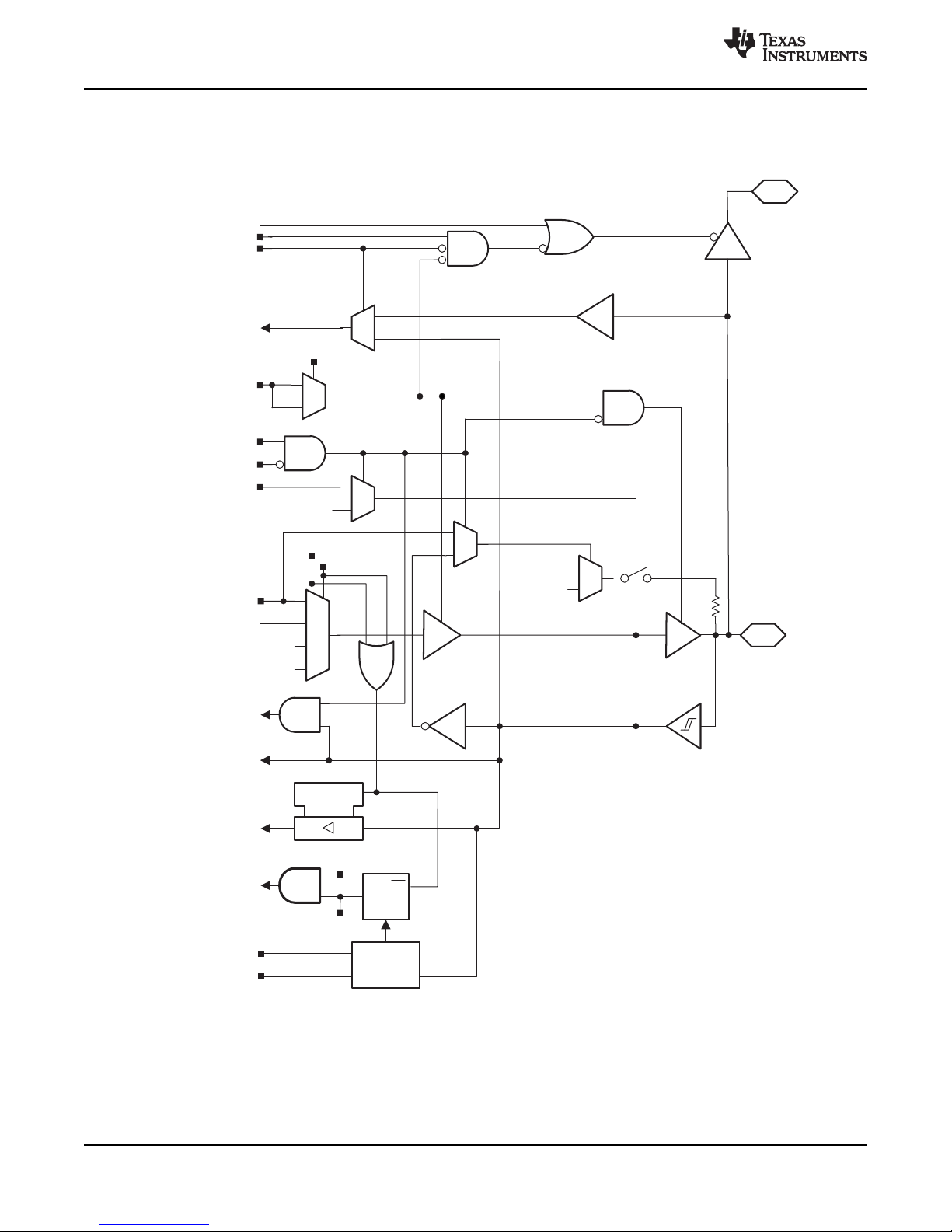
XIN/P2.6/TA0.1
Direction
0: Input
1: Output
To Module
From Module
PxOUT.y
DVSS
DVCC
1
TAx.y
TAxCLK
1
0
PxIN.y
EN
D
PxSEL.y
PxREN.y
1
0
PxDIR.y
1
0
PxSEL2.y
PxSEL.y
1
0
PxSEL.y
1
3
2
1
0
PxSEL2.y
PxIRQ.y
PxIE.y
EN
Set
Q
Interrupt
Edge
Select
PxSEL.y
PxIES.y
PxIFG.y
1
0
XOUT/P2.7
LF off
LFXT1CLK
PxSEL.6, PxSEL.7
BCSCTL3.LFXT1Sx = 11
MSP430G2533,MSP430G2433,MSP430G2333,MSP430G2233
MSP430G2403, MSP430G2303, MSP430G2203
SLAS734G –APRIL 2011–REVISED APRIL 2016
6.10.6 Port P2 Pin Diagram: P2.6, Input/Output With Schmitt Trigger
Figure 6-11 shows the port diagram. Table 6-21 summarizes the selection of the pin functions.
www.ti.com
58
Detailed Description Copyright © 2011–2016, Texas Instruments Incorporated
Product Folder Links: MSP430G2533 MSP430G2433 MSP430G2333 MSP430G2233 MSP430G2403 MSP430G2303
Figure 6-11. Port P2 (P2.6) Diagram
Submit Documentation Feedback
MSP430G2203

MSP430G2533,MSP430G2433,MSP430G2333,MSP430G2233
MSP430G2403, MSP430G2303, MSP430G2203
www.ti.com
SLAS734G –APRIL 2011–REVISED APRIL 2016
Table 6-21. Port P2 (P2.6) Pin Functions
PIN NAME
(P2.x)
XIN
P2.6 P2.x (I/O) I: 0; O: 1
TA0.1 Timer0_A3.TA1 1
Pin Osc Capacitive sensing X
(1) X = don't care
x FUNCTION
XIN 0
6
CONTROL BITS OR SIGNALS
P2DIR.x
P2SEL.6
P2SEL.7
1
1
0
X
1
0
0
X
(1)
P2SEL2.6
P2SEL2.7
0
0
0
0
0
0
1
X
Product Folder Links: MSP430G2533 MSP430G2433 MSP430G2333 MSP430G2233 MSP430G2403 MSP430G2303
Submit Documentation Feedback
MSP430G2203
Detailed DescriptionCopyright © 2011–2016, Texas Instruments Incorporated
59

XOUT/P2.7
Direction
0: Input
1: Output
To Module
From Module
PxOUT.y
DVSS
DVCC
1
TAx.y
TAxCLK
1
0
PxIN.y
EN
D
PxSEL.y
PxREN.y
1
0
PxDIR.y
1
0
PxSEL2.y
PxSEL.y
1
0
PxSEL.y
1
3
2
1
0
PxSEL2.y
PxIRQ.y
PxIE.y
EN
Set
Q
Interrupt
Edge
Select
PxSEL.y
PxIES.y
PxIFG.y
1
0
XIN
LF off
LFXT1CLK
PxSEL.6, PxSEL.7
BCSCTL3.LFXT1Sx = 11
from P2.6
MSP430G2533,MSP430G2433,MSP430G2333,MSP430G2233
MSP430G2403, MSP430G2303, MSP430G2203
SLAS734G –APRIL 2011–REVISED APRIL 2016
6.10.7 Port P2 Pin Diagram: P2.7, Input/Output With Schmitt Trigger
Figure 6-12 shows the port diagram. Table 6-22 summarizes the selection of the pin functions.
www.ti.com
60
Detailed Description Copyright © 2011–2016, Texas Instruments Incorporated
Product Folder Links: MSP430G2533 MSP430G2433 MSP430G2333 MSP430G2233 MSP430G2403 MSP430G2303
Figure 6-12. Port P2 (P2.7) Diagram
Submit Documentation Feedback
MSP430G2203
MSP430G2533,MSP430G2433,MSP430G2333,MSP430G2233
MSP430G2403, MSP430G2303, MSP430G2203
www.ti.com
SLAS734G –APRIL 2011–REVISED APRIL 2016
Table 6-22. Port P2 (P2.7) Pin Functions
PIN NAME
(P2.x)
XOUT/
P2.7/ P2.x (I/O) I: 0; O: 1
Pin Osc Capacitive sensing X
(1) X = don't care
x FUNCTION
XOUT 1
7
CONTROL BITS OR SIGNALS
P2DIR.x
P2SEL.6
P2SEL.7
1
1
0
X
0
X
(1)
P2SEL2.6
P2SEL2.7
0
0
0
0
1
X
Product Folder Links: MSP430G2533 MSP430G2433 MSP430G2333 MSP430G2233 MSP430G2403 MSP430G2303
Submit Documentation Feedback
MSP430G2203
Detailed DescriptionCopyright © 2011–2016, Texas Instruments Incorporated
61
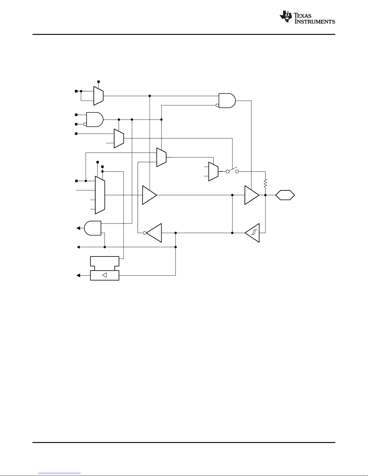
P3.0/TA0.2
P3.1/TA1.0
P3.2/TA1.1
P3.3/TA1.2
P3.4/TA0.0
P3.5/TA0.1
P3.6/TA0.2
P3.7/TA1CLK/CAOUT
Direction
0: Input
1: Output
To Module
From Module
PxOUT.y
DVSS
DVCC
1
TAx.y
TAxCLK
1
0
PxIN.y
EN
D
PxSEL.y
PxREN.y
1
0
PxDIR.y
1
0
PxSEL2.y
PxSEL.y
1
0
PxSEL.y
1
3
2
1
0
PxSEL2.y
MSP430G2533,MSP430G2433,MSP430G2333,MSP430G2233
MSP430G2403, MSP430G2303, MSP430G2203
SLAS734G –APRIL 2011–REVISED APRIL 2016
6.10.8 Port P3 Pin Diagram: P3.0 to P3.7, Input/Output With Schmitt Trigger (RHB and
PW28 Package Only)
Figure 6-13 shows the port diagram. Table 6-23 summarizes the selection of the pin functions.
www.ti.com
62
Detailed Description Copyright © 2011–2016, Texas Instruments Incorporated
Product Folder Links: MSP430G2533 MSP430G2433 MSP430G2333 MSP430G2233 MSP430G2403 MSP430G2303
Figure 6-13. Port P3 (P3.0 to P3.7) Diagram (RHB and PW28 Package Only)
Submit Documentation Feedback
MSP430G2203
MSP430G2533,MSP430G2433,MSP430G2333,MSP430G2233
MSP430G2403, MSP430G2303, MSP430G2203
www.ti.com
SLAS734G –APRIL 2011–REVISED APRIL 2016
Table 6-23. Port P3 (P3.0 to P3.7) Pin Functions (RHB and PW28 Package Only)
PIN NAME
(P3.x)
P3.0/
TA0.2/ Timer0_A3.CCI2A 0 1 0
Pin Osc Capacitive sensing X 0 1
P3.1/
TA1.0/ Timer1_A3.TA0 1 1 0
Pin Osc Capacitive sensing X 0 1
P3.2/
TA1.1/ Timer1_A3.TA1 1 1 0
Pin Osc Capacitive sensing X 0 1
P3.3/
TA1.2/ Timer1_A3.TA2 1 1 0
Pin Osc Capacitive sensing X 0 1
P3.4/
TA0.0/ Timer0_A3.TA0 1 1 0
Pin Osc Capacitive sensing X 0 1
P3.5/
TA0.1/ Timer0_A3.TA1 1 1 0
Pin Osc Capacitive sensing X 0 1
P3.6/
TA0.2/ Timer0_A3.TA2 1 1 0
Pin Osc Capacitive sensing X 0 1
P3.7/
TA1CLK/ Timer1_A3.TACLK 0 1 0
Pin Osc Capacitive sensing X 0 1
(1) X = don't care
x FUNCTION
P3.x (I/O) I: 0; O: 1 0 0
0
Timer0_A3.TA2 1 1 0
P3.x (I/O) I: 0; O: 1 0 0
1
P3.x (I/O) I: 0; O: 1 0 0
2
P3.x (I/O) I: 0; O: 1 0 0
3
P3.x (I/O) I: 0; O: 1 0 0
4
P3.x (I/O) I: 0; O: 1 0 0
5
P3.x (I/O) I: 0; O: 1 0 0
6
P3.x (I/O) I: 0; O: 1 0 0
7
CONTROL BITS OR SIGNALS
P3DIR.x P3SEL.x P3SEL2.x
(1)
Product Folder Links: MSP430G2533 MSP430G2433 MSP430G2333 MSP430G2233 MSP430G2403 MSP430G2303
Submit Documentation Feedback
MSP430G2203
Detailed DescriptionCopyright © 2011–2016, Texas Instruments Incorporated
63

MSP430G2533,MSP430G2433,MSP430G2333,MSP430G2233
MSP430G2403, MSP430G2303, MSP430G2203
SLAS734G –APRIL 2011–REVISED APRIL 2016
7 Device and Documentation Support
7.1 Getting Started and Next Steps
For more information on the MSP430™ family of devices and the tools and libraries that are available to
help with your development, visit the Getting Started page.
7.2 Device Nomenclature
To designate the stages in the product development cycle, TI assigns prefixes to the part numbers of all
MSP430 MCU devices and support tools. Each MSP430 MCU commercial family member has one of
three prefixes: MSP, PMS, or XMS (for example, MSP430F5438A). TI recommends two of three possible
prefix designators for its support tools: MSP and MSPX. These prefixes represent evolutionary stages of
product development from engineering prototypes (with XMS for devices and MSPX for tools) through fully
qualified production devices and tools (with MSP for devices and MSP for tools).
Device development evolutionary flow:
XMS – Experimental device that is not necessarily representative of the electrical specifications for the
final device
PMS – Final silicon die that conforms to the electrical specifications for the device but has not completed
quality and reliability verification
www.ti.com
MSP – Fully qualified production device
Support tool development evolutionary flow:
MSPX – Development-support product that has not yet completed TI's internal qualification testing.
MSP – Fully-qualified development-support product
XMS and PMS devices and MSPX development-support tools are shipped against the following
disclaimer:
"Developmental product is intended for internal evaluation purposes."
MSP devices and MSP development-support tools have been characterized fully, and the quality and
reliability of the device have been demonstrated fully. TI's standard warranty applies.
Predictions show that prototype devices (XMS and PMS) have a greater failure rate than the standard
production devices. TI recommends that these devices not be used in any production system because
their expected end-use failure rate still is undefined. Only qualified production devices are to be used.
TI device nomenclature also includes a suffix with the device family name. This suffix indicates the
package type (for example, PZP) and temperature range (for example, T). Figure 7-1 provides a legend
for reading the complete device name for any family member.
64
Device and Documentation Support Copyright © 2011–2016, Texas Instruments Incorporated
Product Folder Links: MSP430G2533 MSP430G2433 MSP430G2333 MSP430G2233 MSP430G2403 MSP430G2303
Submit Documentation Feedback
MSP430G2203

Processor Family
CC = Embedded RF Radio
MSP = Mixed-Signal Processor
XMS = Experimental Silicon
PMS = Prototype Device
MCU Platform 430 = MSP430 low-power microcontroller platform
Device Type Memory Type
C = ROM
F = Flash
FR = FRAM
G = Flash or FRAM (Value Line)
L = No Nonvolatile Memory
Specialized Application
AFE = Analog Front End
BT = Preprogrammed with
BQ = Contactless Power
CG = ROM Medical
FE = Flash Energy Meter
FG = Flash Medical
FW = Flash Electronic Flow Meter
Bluetooth
Series 1 Series = Up to 8 MHz
2 Series = Up to 16 MHz
3 Series = Legacy
4 Series = Up to 16 MHz with LCD
5 Series = Up to 25 MHz
6 Series = Up to 25 MHz with LCD
0 = Low-Voltage Series
Feature Set Various Levels of Integration Within a Series
Optional: A = Revision N/A
Optional: Temperature Range S = 0°C to 50 C
C to 70 C
I = 40 C to 85 C
T = –40 C to 105 C
°
C = 0° °
– ° °
° °
Packaging
http://www.ti.com/packaging
Optional: Tape and Reel T = Small Reel
R = Large Reel
No Markings = Tube or Tray
Optional: Additional Features -EP = Enhanced Product ( 40°C to 105°C)
-HT = Extreme Temperature Parts ( 55°C to 150°C)
-Q1 = Automotive Q100 Qualified
–
–
MSP 430 F 5 438 A I ZQW T -EP
Processor Family
Series
Optional: Temperature Range
MCU Platform
Packaging
Device Type
Optional: A = Revision
Optional: Tape and Reel
Feature Set
Optional: Additional Features
www.ti.com
MSP430G2533,MSP430G2433,MSP430G2333,MSP430G2233
MSP430G2403, MSP430G2303, MSP430G2203
SLAS734G –APRIL 2011–REVISED APRIL 2016
Product Folder Links: MSP430G2533 MSP430G2433 MSP430G2333 MSP430G2233 MSP430G2403 MSP430G2303
Figure 7-1. Device Nomenclature
Submit Documentation Feedback
MSP430G2203
Device and Documentation SupportCopyright © 2011–2016, Texas Instruments Incorporated
65

MSP430G2533,MSP430G2433,MSP430G2333,MSP430G2233
MSP430G2403, MSP430G2303, MSP430G2203
SLAS734G –APRIL 2011–REVISED APRIL 2016
7.3 Tools and Software
All MSP microcontrollers are supported by a wide variety of software and hardware development tools.
Tools are available from TI and various third parties. See them all at MSP Tools.
Table 7-1 lists the debug features of these devices. See the Code Composer Studio for MSP430 User's
Guide (SLAU157) for details on the available features.
Table 7-1. Hardware Features
www.ti.com
MSP430
ARCHITECTURE
MSP430 Yes Yes 2 No Yes No No No
4-WIRE
JTAG
2-WIRE
JTAG
BREAK-
POINTS
(N)
RANGE
BREAK-
POINTS
CLOCK
CONTROL
STATE
SEQUENCER
TRACE
BUFFER
DEBUGGING
Design Kits and Evaluation Modules
28-Pin Target Development Board and MSP-FET USB Programmer Bundle for MSP430F2x and
MSP430G2x MCUs The MSP-FET430U28A kit includes all of the hardware and software
required to quickly begin application development on the MSP430 MCU. This kit includes a
ZIF socket target board (MSP-TS430PW28A) that accepts some MSP430 devices in 20- or
28-pin TSSOP packages (TI Package Code: PW). It is also bundled with a USB flash
emulation tool (MSP-FET) that interfaces the target board to a PC, allowing developers to
program and debug their MSP430 devices through in-system emulation through the JTAG
interface or the pin-saving Spy Bi-Wire (2-wire JTAG) protocol.
MSP430 LaunchPad™ Value Line Development Kit The MSP-EXP430G2 LaunchPad Development Kit
is an easy-to-use microcontroller development board for the low-power and low-cost
MSP430G2x MCUs. It has on-board emulation for programming and debugging and features
a 14- or 20-pin DIP socket, on-board buttons and LEDs and BoosterPack Plug-in Module
pinouts that support a wide range of modules for added functionality such as wireless,
displays, and more.
MSP430 Capacitive Touch BoosterPack™ Plug-in Module The Capacitive Touch BoosterPack
(430BOOST-SENSE1) is a plug-in module for MCU LaunchPad Development Kits. This
BoosterPack also includes a preprogrammed MSP430G2452IN20 Value Line device for the
MSP-EXP430G2 LaunchPad. Developers can use this BoosterPack as a solution for adding
capacitive touch differentiation in many applications such as consumer electronics, point of
sales machines, and other devices with a physical button.
LPMx.5
SUPPORT
Software
MSP430G2x53, MSP430G2x33, MSP430G2x13, MSP430G2x03 Code Examples C Code examples are
available for every MSP device that configures each of the integrated peripherals for various
application needs.
MSPWare™ Software MSPWare software is a collection of code examples, data sheets, and other
design resources for all MSP devices delivered in a convenient package. In addition to
providing a complete collection of existing MSP design resources, MSPWare software also
includes a high-level API called MSP Driver Library. This library makes it easy to program
MSP hardware. MSPWare software is available as a component of CCS or as a stand-alone
package.
MSP Driver Library Driver Library's abstracted API keeps you above the bits and bytes of the MSP430
hardware by providing easy-to-use function calls. Thorough documentation is delivered
through a helpful API Guide, which includes details on each function call and the recognized
parameters. Developers can use Driver Library functions to write complete projects with
minimal overhead.
66
Device and Documentation Support Copyright © 2011–2016, Texas Instruments Incorporated
Product Folder Links: MSP430G2533 MSP430G2433 MSP430G2333 MSP430G2233 MSP430G2403 MSP430G2303
Submit Documentation Feedback
MSP430G2203

www.ti.com
Capacitive Touch Software Library Free C libraries for enabling capacitive touch capabilities on
MSP EnergyTrace™ Technology EnergyTrace technology for MSP430 microcontrollers is an energy-
ULP (Ultra-Low Power) Advisor ULP Advisor™ software is a tool for guiding developers to write more
IEC60730 Software Package The IEC60730 MSP430 software package was developed to be useful in
MSP430G2533,MSP430G2433,MSP430G2333,MSP430G2233
MSP430G2403, MSP430G2303, MSP430G2203
SLAS734G –APRIL 2011–REVISED APRIL 2016
MSP430 MCUs and MSP432 MCUs. The MSP430 MCU version of the library features
several capacitive touch implementations including the RO and RC method.
based code analysis tool that measures and displays the application’s energy profile and
helps to optimize it for ultra-low-power consumption.
efficient code to fully utilize the unique ultra-low power features of MSP and MSP432
microcontrollers. Aimed at both experienced and new microcontroller developers, ULP
Advisor checks your code against a thorough ULP checklist to squeeze every last nano amp
out of your application. At build time, ULP Advisor will provide notifications and remarks to
highlight areas of your code that can be further optimized for lower power.
assisting customers in complying with IEC 60730-1:2010 (Automatic Electrical Controls for
Household and Similar Use – Part 1: General Requirements) for up to Class B products,
which includes home appliances, arc detectors, power converters, power tools, e-bikes, and
many others. The IEC60730 MSP430 software package can be embedded in customer
applications running on MSP430s to help simplify the customer’s certification efforts of
functional safety-compliant consumer devices to IEC 60730-1:2010 Class B.
Fixed-Point Math Library for MSP The MSP IQmath and Qmath Libraries are a collection of highly
optimized and high-precision mathematical functions for C programmers to seamlessly port a
floating-point algorithm into fixed-point code on MSP430 and MSP432 devices. These
routines are typically used in computationally intensive real-time applications where optimal
execution speed, high accuracy, and ultra-low energy are critical. By using the IQmath and
Qmath libraries, it is possible to achieve execution speeds considerably faster and energy
consumption considerably lower than equivalent code written using floating-point math.
Development Tools
Code Composer Studio™ Integrated Development Environment for MSP Microcontrollers Code
Composer Studio is an integrated development environment (IDE) that supports all MSP
microcontroller devices. Code Composer Studio comprises a suite of embedded software
utilities used to develop and debug embedded applications. It includes an optimizing C/C++
compiler, source code editor, project build environment, debugger, profiler, and many other
features. The intuitive IDE provides a single user interface taking you through each step of
the application development flow. Familiar utilities and interfaces allow users to get started
faster than ever before. Code Composer Studio combines the advantages of the Eclipse
software framework with advanced embedded debug capabilities from TI resulting in a
compelling feature-rich development environment for embedded developers. When using
CCS with an MSP MCU, a unique and powerful set of plugins and embedded software
utilities are made available to fully leverage the MSP microcontroller.
Grace – Graphical Peripheral Configuration Tool Enable and configure ADCs, DACs, timers, clocks,
serial communication interfaces, and more, by interacting with buttons, drop-down menus,
and text fields. Navigate through the MSP430 MCUs highly integrated peripheral set with
ease.
MSP Flasher - Command Line Programmer MSP Flasher is an open-source shell-based interface for
programming MSP microcontrollers through a FET programmer or eZ430 using JTAG or
Spy-Bi-Wire (SBW) communication. MSP Flasher can download binary files (.txt or .hex) files
directly to the MSP microcontroller without an IDE.
Product Folder Links: MSP430G2533 MSP430G2433 MSP430G2333 MSP430G2233 MSP430G2403 MSP430G2303
Submit Documentation Feedback
MSP430G2203
Device and Documentation SupportCopyright © 2011–2016, Texas Instruments Incorporated
67

MSP430G2533,MSP430G2433,MSP430G2333,MSP430G2233
MSP430G2403, MSP430G2303, MSP430G2203
SLAS734G –APRIL 2011–REVISED APRIL 2016
MSP MCU Programmer and Debugger The MSP-FET is a powerful emulation development tool – often
called a debug probe – which allows users to quickly begin application development on MSP
low-power microcontrollers (MCU). Creating MCU software usually requires downloading the
resulting binary program to the MSP device for validation and debugging. The MSP-FET
provides a debug communication pathway between a host computer and the target MSP.
Furthermore, the MSP-FET also provides a Backchannel UART connection between the
computer's USB interface and the MSP UART. This affords the MSP programmer a
convenient method for communicating serially between the MSP and a terminal running on
the computer. It also supports loading programs (often called firmware) to the MSP target
using the BSL (bootloader) through the UART and I2C communication protocols.
MSP-GANG Production Programmer The MSP Gang Programmer is an MSP430 or MSP432 device
programmer that can program up to eight identical MSP430 or MSP432 Flash or FRAM
devices at the same time. The MSP Gang Programmer connects to a host PC using a
standard RS-232 or USB connection and provides flexible programming options that allow
the user to fully customize the process. The MSP Gang Programmer is provided with an
expansion board, called the Gang Splitter, that implements the interconnections between the
MSP Gang Programmer and multiple target devices. Eight cables are provided that connect
the expansion board to eight target devices (through JTAG or Spy-Bi-Wire connectors). The
programming can be done with a PC or as a stand-alone device. A PC-side graphical user
interface is also available and is DLL-based.
www.ti.com
7.4 Documentation Support
The following documents describe the MSP430G2x33 and MSP430G2x03 devices. Copies of these
documents are available on the Internet at www.ti.com.
Receiving Notification of Document Updates
To receive notification of documentation updates—including silicon errata—go to the product folder for
your device on ti.com (for example, MSP430G2533). In the upper right corner, click the "Alert me" button.
This registers you to receive a weekly digest of product information that has changed (if any). For change
details, check the revision history of any revised document.
Errata
MSP430G2533 Device Erratasheet Describes the known exceptions to the functional specifications for
the MSP430G2533 device.
MSP430G2433 Device Erratasheet Describes the known exceptions to the functional specifications for
the MSP430G2433 device.
MSP430G2333 Device Erratasheet Describes the known exceptions to the functional specifications for
the MSP430G2333 device.
MSP430G2233 Device Erratasheet Describes the known exceptions to the functional specifications for
the MSP430G2233 device.
MSP430G2403 Device Erratasheet Describes the known exceptions to the functional specifications for
the MSP430G2403 device.
MSP430G2303 Device Erratasheet Describes the known exceptions to the functional specifications for
the MSP430G2303 device.
MSP430G2203 Device Erratasheet Describes the known exceptions to the functional specifications for
the MSP430G2203 device.
68
Device and Documentation Support Copyright © 2011–2016, Texas Instruments Incorporated
Product Folder Links: MSP430G2533 MSP430G2433 MSP430G2333 MSP430G2233 MSP430G2403 MSP430G2303
Submit Documentation Feedback
MSP430G2203

www.ti.com
User's Guides
MSP430x2xx Family User's Guide Detailed information on the modules and peripherals available in this
Code Composer Studio v6.1 for MSP430 User's Guide This manual describes the use of TI Code
IAR Embedded Workbench Version 3+ for MSP430 User's Guide This manual describes the use of
MSP430 Programming With the Bootloader (BSL) The MSP430 bootloader (BSL, formerly known as
MSP430 Programming Via the JTAG Interface This document describes the functions that are required
MSP430G2533,MSP430G2433,MSP430G2333,MSP430G2233
MSP430G2403, MSP430G2303, MSP430G2203
SLAS734G –APRIL 2011–REVISED APRIL 2016
device family.
Composer Studio IDE v6.1 (CCS v6.1) with the MSP430 ultra-low-power microcontrollers.
This document applies only for the Windows version of the Code Composer Studio IDE. The
Linux version is similar and, therefore, is not described separately.
IAR Embedded Workbench (EW430) with the MSP430 ultra-low-power microcontrollers.
the bootstrap loader) allows users to communicate with embedded memory in the MSP430
microcontroller during the prototyping phase, final production, and in service. Both the
programmable memory (flash memory) and the data memory (RAM) can be modified as
required. Do not confuse the bootloader with the bootstrap loader programs found in some
digital signal processors (DSPs) that automatically load program code (and data) from
external memory to the internal memory of the DSP.
to erase, program, and verify the memory module of the MSP430 flash-based and FRAMbased microcontroller families using the JTAG communication port. In addition, it describes
how to program the JTAG access security fuse that is available on all MSP430 devices. This
document describes device access using both the standard 4-wire JTAG interface and the 2wire JTAG interface, which is also referred to as Spy-Bi-Wire (SBW).
MSP430 Hardware Tools User's Guide This manual describes the hardware of the TI MSP-FET430
Flash Emulation Tool (FET). The FET is the program development tool for the MSP430 ultralow-power microcontroller. Both available interface types, the parallel port interface and the
USB interface, are described.
Application Reports
MSP430 32-kHz Crystal Oscillators Selection of the right crystal, correct load circuit, and proper board
layout are important for a stable crystal oscillator. This application report summarizes crystal
oscillator function and explains the parameters to select the correct crystal for MSP430 ultralow-power operation. In addition, hints and examples for correct board layout are given. The
document also contains detailed information on the possible oscillator tests to ensure stable
oscillator operation in mass production.
MSP430 System-Level ESD Considerations System-Level ESD has become increasingly demanding
with silicon technology scaling towards lower voltages and the need for designing costeffective and ultra-low-power components. This application report addresses three different
ESD topics to help board designers and OEMs understand and design robust system-level
designs: (1) Component-level ESD testing and system-level ESD testing, their differences
and why component-level ESD rating does not ensure system-level robustness. (2) General
design guidelines for system-level ESD protection at different levels including enclosures,
cables, PCB layout, and on-board ESD protection devices. (3) Introduction to System
Efficient ESD Design (SEED), a co-design methodology of on-board and on-chip ESD
protection to achieve system-level ESD robustness, with example simulations and test
results. A few real-world system-level ESD protection design examples and their results are
also discussed.
Product Folder Links: MSP430G2533 MSP430G2433 MSP430G2333 MSP430G2233 MSP430G2403 MSP430G2303
Submit Documentation Feedback
MSP430G2203
Device and Documentation SupportCopyright © 2011–2016, Texas Instruments Incorporated
69

MSP430G2533,MSP430G2433,MSP430G2333,MSP430G2233
MSP430G2403, MSP430G2303, MSP430G2203
SLAS734G –APRIL 2011–REVISED APRIL 2016
General Oversampling of MSP ADCs for Higher Resolution Multiple MSP ultra-low-power
microcontrollers offer analog-to-digital converters (ADCs) to convert physical quantities into
digital numbers, a function that is widely used across numerous applications. There are
times, however, when a customer design demands a higher resolution than the ADC of the
selected MSP can offer. This application report, which is based on the previously-published
Oversampling the ADC12 for Higher Resolution (SLAA323), therefore describes how an
oversampling method can be incorporated to increase ADC resolution past the currently
available number of bits.
Capacitive Touch Hardware Design Guide Capacitive touch detection is sometimes considered more
art than science. This often results in multiple design iterations before the optimum
performance is achieved. There are, however, good design practices for circuit layout and
principles of materials that need to be understood to keep the number of iterations to a
minimum. This design guide describes a process for creating and designing capacitive touch
solutions, starting with the schematic, working through the mechanicals, and finally designing
the electrodes for the application.
Capacitive Touch Sensing, MSP430 Slider and Wheel Tuning Guide This application report provides
guidelines on how to tune capacitive touch sliders and wheels running on the MSP430™
microcontrollers. It identifies the hardware and software parameters as well as explains the
steps used in tuning sliders and wheels. The slider and wheel tuning is based on the APIs
defined in the Capacitive Touch Sense Library (CAPSENSELIBRARY).
www.ti.com
Capacitive Touch Sensing, MSP430 Button Gate Time Optimization and Tuning Guide MSP430™
microcontroller based capacitive touch buttons can offer increased performance when
properly optimized and tuned for their specific application. Performance benefits that result
from button optimization can include, but are not limited to, decreased power consumption,
improved response time, and the ability to grow a design to include more buttons. This
application report provides the reader with a starting point for button design at the system
and software level.
7.5 Related Links
Table 7-2 lists quick access links. Categories include technical documents, support and community
resources, tools and software, and quick access to sample or buy.
Table 7-2. Related Links
PARTS PRODUCT FOLDER SAMPLE & BUY
MSP430G2533 Click here Click here Click here Click here Click here
MSP430G2433 Click here Click here Click here Click here Click here
MSP430G2333 Click here Click here Click here Click here Click here
MSP430G2233 Click here Click here Click here Click here Click here
MSP430G2403 Click here Click here Click here Click here Click here
MSP430G2303 Click here Click here Click here Click here Click here
MSP430G2203 Click here Click here Click here Click here Click here
TECHNICAL
DOCUMENTS
TOOLS &
SOFTWARE
SUPPORT &
COMMUNITY
70
Device and Documentation Support Copyright © 2011–2016, Texas Instruments Incorporated
Product Folder Links: MSP430G2533 MSP430G2433 MSP430G2333 MSP430G2233 MSP430G2403 MSP430G2303
Submit Documentation Feedback
MSP430G2203

www.ti.com
7.6 Community Resources
The following links connect to TI community resources. Linked contents are provided "AS IS" by the
respective contributors. They do not constitute TI specifications and do not necessarily reflect TI's views;
see TI's Terms of Use.
TI E2E™ Community
TI's Engineer-to-Engineer (E2E) Community. Created to foster collaboration among engineers. At
e2e.ti.com, you can ask questions, share knowledge, explore ideas, and help solve problems with fellow
engineers.
TI Embedded Processors Wiki
Texas Instruments Embedded Processors Wiki. Established to help developers get started with embedded
processors from Texas Instruments and to foster innovation and growth of general knowledge about the
hardware and software surrounding these devices.
7.7 Trademarks
MSP430, LaunchPad, BoosterPack, MSPWare, EnergyTrace, ULP Advisor, Code Composer Studio, E2E
are trademarks of Texas Instruments.
All other trademarks are the property of their respective owners.
7.8 Electrostatic Discharge Caution
These devices have limited built-in ESD protection. The leads should be shorted together or the device placed in conductive foam
during storage or handling to prevent electrostatic damage to the MOS gates.
MSP430G2533,MSP430G2433,MSP430G2333,MSP430G2233
MSP430G2403, MSP430G2303, MSP430G2203
SLAS734G –APRIL 2011–REVISED APRIL 2016
7.9 Glossary
TI Glossary This glossary lists and explains terms, acronyms, and definitions.
Product Folder Links: MSP430G2533 MSP430G2433 MSP430G2333 MSP430G2233 MSP430G2403 MSP430G2303
Submit Documentation Feedback
MSP430G2203
Device and Documentation SupportCopyright © 2011–2016, Texas Instruments Incorporated
71

MSP430G2533,MSP430G2433,MSP430G2333,MSP430G2233
MSP430G2403, MSP430G2303, MSP430G2203
SLAS734G –APRIL 2011–REVISED APRIL 2016
8 Mechanical, Packaging, and Orderable Information
The following pages include mechanical, packaging, and orderable information. This information is the
most current data available for the designated devices. This data is subject to change without notice and
revision of this document. For browser-based versions of this data sheet, refer to the left-hand navigation.
www.ti.com
72
Mechanical, Packaging, and Orderable Information Copyright © 2011–2016, Texas Instruments Incorporated
Product Folder Links: MSP430G2533 MSP430G2433 MSP430G2333 MSP430G2233 MSP430G2403 MSP430G2303
Submit Documentation Feedback
MSP430G2203

PACKAGE OPTION ADDENDUM
www.ti.com
30-Apr-2015
Addendum-Page 1
PACKAGING INFORMATION
Orderable Device Status
(1)
Package Type Package
Drawing
Pins Package
Qty
Eco Plan
(2)
Lead/Ball Finish
(6)
MSL Peak Temp
(3)
Op Temp (°C) Device Marking
(4/5)
Samples
MSP430G2203IN20 ACTIVE PDIP N 20 20 Pb-Free
(RoHS)
CU NIPDAU Level-1-260C-UNLIM -40 to 85 M430G2203
MSP430G2203IPW20 ACTIVE TSSOP PW 20 70 Green (RoHS
& no Sb/Br)
CU NIPDAU Level-1-260C-UNLIM -40 to 85 430G2203
MSP430G2203IPW20R ACTIVE TSSOP PW 20 2000 Green (RoHS
& no Sb/Br)
CU NIPDAU Level-1-260C-UNLIM -40 to 85 430G2203
MSP430G2203IPW28 ACTIVE TSSOP PW 28 50 Green (RoHS
& no Sb/Br)
CU NIPDAU Level-1-260C-UNLIM -40 to 85 430G2203
MSP430G2203IPW28R ACTIVE TSSOP PW 28 2000 Green (RoHS
& no Sb/Br)
CU NIPDAU Level-1-260C-UNLIM -40 to 85 430G2203
MSP430G2203IRHB32R ACTIVE VQFN RHB 32 3000 Green (RoHS
& no Sb/Br)
CU NIPDAU Level-2-260C-1 YEAR -40 to 85 MSP430
G2203
MSP430G2233IN20 ACTIVE PDIP N 20 20 Pb-Free
(RoHS)
CU NIPDAU Level-1-260C-UNLIM -40 to 85 M430G2233
MSP430G2233IPW20 ACTIVE TSSOP PW 20 70 Green (RoHS
& no Sb/Br)
CU NIPDAU Level-1-260C-UNLIM -40 to 85 430G2233
MSP430G2233IPW20R ACTIVE TSSOP PW 20 2000 Green (RoHS
& no Sb/Br)
CU NIPDAU Level-1-260C-UNLIM -40 to 85 430G2233
MSP430G2233IPW28 ACTIVE TSSOP PW 28 50 Green (RoHS
& no Sb/Br)
CU NIPDAU Level-1-260C-UNLIM -40 to 85 430G2233
MSP430G2233IPW28R ACTIVE TSSOP PW 28 2000 Green (RoHS
& no Sb/Br)
CU NIPDAU Level-1-260C-UNLIM -40 to 85 430G2233
MSP430G2233IRHB32R ACTIVE VQFN RHB 32 3000 Green (RoHS
& no Sb/Br)
CU NIPDAU Level-2-260C-1 YEAR -40 to 85 MSP430
G2233
MSP430G2233IRHB32T ACTIVE VQFN RHB 32 250 Green (RoHS
& no Sb/Br)
CU NIPDAU Level-2-260C-1 YEAR -40 to 85 MSP430
G2233
MSP430G2303IN20 ACTIVE PDIP N 20 20 Pb-Free
(RoHS)
CU NIPDAU Level-1-260C-UNLIM -40 to 85 M430G2303
MSP430G2303IPW20 ACTIVE TSSOP PW 20 70 Green (RoHS
& no Sb/Br)
CU NIPDAU Level-1-260C-UNLIM -40 to 85 430G2303
MSP430G2303IPW20R ACTIVE TSSOP PW 20 2000 Green (RoHS
& no Sb/Br)
CU NIPDAU Level-1-260C-UNLIM -40 to 85 430G2303
MSP430G2303IPW28 ACTIVE TSSOP PW 28 50 Green (RoHS
& no Sb/Br)
CU NIPDAU Level-1-260C-UNLIM -40 to 85 430G2303

PACKAGE OPTION ADDENDUM
www.ti.com
30-Apr-2015
Addendum-Page 2
Orderable Device Status
(1)
Package Type Package
Drawing
Pins Package
Qty
Eco Plan
(2)
Lead/Ball Finish
(6)
MSL Peak Temp
(3)
Op Temp (°C) Device Marking
(4/5)
Samples
MSP430G2303IPW28R ACTIVE TSSOP PW 28 2000 Green (RoHS
& no Sb/Br)
CU NIPDAU Level-1-260C-UNLIM -40 to 85 430G2303
MSP430G2303IRHB32R ACTIVE VQFN RHB 32 3000 Green (RoHS
& no Sb/Br)
CU NIPDAU Level-2-260C-1 YEAR -40 to 85 MSP430
G2303
MSP430G2303IRHB32T ACTIVE VQFN RHB 32 250 Green (RoHS
& no Sb/Br)
CU NIPDAU Level-2-260C-1 YEAR -40 to 85 MSP430
G2303
MSP430G2333IN20 ACTIVE PDIP N 20 20 Pb-Free
(RoHS)
CU NIPDAU Level-1-260C-UNLIM -40 to 85 M430G2333
MSP430G2333IPW20 ACTIVE TSSOP PW 20 70 Green (RoHS
& no Sb/Br)
CU NIPDAU Level-1-260C-UNLIM -40 to 85 430G2333
MSP430G2333IPW20R ACTIVE TSSOP PW 20 2000 Green (RoHS
& no Sb/Br)
CU NIPDAU Level-1-260C-UNLIM -40 to 85 430G2333
MSP430G2333IPW28 ACTIVE TSSOP PW 28 50 Green (RoHS
& no Sb/Br)
CU NIPDAU Level-1-260C-UNLIM -40 to 85 430G2333
MSP430G2333IPW28R ACTIVE TSSOP PW 28 2000 Green (RoHS
& no Sb/Br)
CU NIPDAU Level-1-260C-UNLIM -40 to 85 430G2333
MSP430G2333IRHB32R ACTIVE VQFN RHB 32 3000 Green (RoHS
& no Sb/Br)
CU NIPDAU Level-2-260C-1 YEAR -40 to 85 MSP430
G2333
MSP430G2333IRHB32T ACTIVE VQFN RHB 32 250 Green (RoHS
& no Sb/Br)
CU NIPDAU Level-2-260C-1 YEAR -40 to 85 MSP430
G2333
MSP430G2403IN20 ACTIVE PDIP N 20 20 Pb-Free
(RoHS)
CU NIPDAU Level-1-260C-UNLIM -40 to 85 M430G2403
MSP430G2403IPW20 ACTIVE TSSOP PW 20 70 Green (RoHS
& no Sb/Br)
CU NIPDAU Level-1-260C-UNLIM -40 to 85 430G2403
MSP430G2403IPW20R ACTIVE TSSOP PW 20 2000 Green (RoHS
& no Sb/Br)
CU NIPDAU Level-1-260C-UNLIM -40 to 85 430G2403
MSP430G2403IPW28 ACTIVE TSSOP PW 28 50 Green (RoHS
& no Sb/Br)
CU NIPDAU Level-1-260C-UNLIM -40 to 85 430G2403
MSP430G2403IPW28R ACTIVE TSSOP PW 28 2000 Green (RoHS
& no Sb/Br)
CU NIPDAU Level-1-260C-UNLIM -40 to 85 430G2403
MSP430G2403IRHB32R ACTIVE VQFN RHB 32 3000 Green (RoHS
& no Sb/Br)
CU NIPDAU Level-2-260C-1 YEAR -40 to 85 MSP430
G2403
MSP430G2403IRHB32T ACTIVE VQFN RHB 32 250 Green (RoHS
& no Sb/Br)
CU NIPDAU Level-2-260C-1 YEAR -40 to 85 MSP430
G2403
MSP430G2433IN20 ACTIVE PDIP N 20 20 Pb-Free
(RoHS)
CU NIPDAU Level-1-260C-UNLIM -40 to 85 M430G2433

PACKAGE OPTION ADDENDUM
www.ti.com
30-Apr-2015
Addendum-Page 3
Orderable Device Status
(1)
Package Type Package
Drawing
Pins Package
Qty
Eco Plan
(2)
Lead/Ball Finish
(6)
MSL Peak Temp
(3)
Op Temp (°C) Device Marking
(4/5)
Samples
MSP430G2433IPW20 ACTIVE TSSOP PW 20 70 Green (RoHS
& no Sb/Br)
CU NIPDAU Level-1-260C-UNLIM -40 to 85 430G2433
MSP430G2433IPW20R ACTIVE TSSOP PW 20 2000 Green (RoHS
& no Sb/Br)
CU NIPDAU Level-1-260C-UNLIM -40 to 85 430G2433
MSP430G2433IPW28 ACTIVE TSSOP PW 28 50 Green (RoHS
& no Sb/Br)
CU NIPDAU Level-1-260C-UNLIM -40 to 85 430G2433
MSP430G2433IPW28R ACTIVE TSSOP PW 28 2000 Green (RoHS
& no Sb/Br)
CU NIPDAU Level-1-260C-UNLIM -40 to 85 430G2433
MSP430G2433IRHB32R ACTIVE VQFN RHB 32 3000 Green (RoHS
& no Sb/Br)
CU NIPDAU Level-2-260C-1 YEAR -40 to 85 MSP430
G2433
MSP430G2433IRHB32T ACTIVE VQFN RHB 32 250 Green (RoHS
& no Sb/Br)
CU NIPDAU Level-2-260C-1 YEAR -40 to 85 MSP430
G2433
MSP430G2533IN20 ACTIVE PDIP N 20 20 Pb-Free
(RoHS)
CU NIPDAU Level-1-260C-UNLIM -40 to 85 M430G2533
MSP430G2533IPW20 ACTIVE TSSOP PW 20 70 Green (RoHS
& no Sb/Br)
CU NIPDAU Level-1-260C-UNLIM -40 to 85 430G2533
MSP430G2533IPW20R ACTIVE TSSOP PW 20 2000 Green (RoHS
& no Sb/Br)
CU NIPDAU Level-1-260C-UNLIM -40 to 85 430G2533
MSP430G2533IPW28 ACTIVE TSSOP PW 28 50 Green (RoHS
& no Sb/Br)
CU NIPDAU Level-1-260C-UNLIM -40 to 85 430G2533
MSP430G2533IPW28R ACTIVE TSSOP PW 28 2000 Green (RoHS
& no Sb/Br)
CU NIPDAU Level-1-260C-UNLIM -40 to 85 430G2533
MSP430G2533IRHB32R ACTIVE VQFN RHB 32 3000 Green (RoHS
& no Sb/Br)
CU NIPDAU Level-2-260C-1 YEAR -40 to 85 MSP430
G2533
MSP430G2533IRHB32T ACTIVE VQFN RHB 32 250 Green (RoHS
& no Sb/Br)
CU NIPDAU Level-2-260C-1 YEAR -40 to 85 MSP430
G2533
(1)
The marketing status values are defined as follows:
ACTIVE: Product device recommended for new designs.
LIFEBUY: TI has announced that the device will be discontinued, and a lifetime-buy period is in effect.
NRND: Not recommended for new designs. Device is in production to support existing customers, but TI does not recommend using this part in a new design.
PREVIEW: Device has been announced but is not in production. Samples may or may not be available.
OBSOLETE: TI has discontinued the production of the device.
(2)
Eco Plan - The planned eco-friendly classification: Pb-Free (RoHS), Pb-Free (RoHS Exempt), or Green (RoHS & no Sb/Br) - please check http://www.ti.com/productcontent for the latest availability
information and additional product content details.
TBD: The Pb-Free/Green conversion plan has not been defined.

PACKAGE OPTION ADDENDUM
www.ti.com
30-Apr-2015
Addendum-Page 4
Pb-Free (RoHS): TI's terms "Lead-Free" or "Pb-Free" mean semiconductor products that are compatible with the current RoHS requirements for all 6 substances, including the requirement that
lead not exceed 0.1% by weight in homogeneous materials. Where designed to be soldered at high temperatures, TI Pb-Free products are suitable for use in specified lead-free processes.
Pb-Free (RoHS Exempt): This component has a RoHS exemption for either 1) lead-based flip-chip solder bumps used between the die and package, or 2) lead-based die adhesive used between
the die and leadframe. The component is otherwise considered Pb-Free (RoHS compatible) as defined above.
Green (RoHS & no Sb/Br): TI defines "Green" to mean Pb-Free (RoHS compatible), and free of Bromine (Br) and Antimony (Sb) based flame retardants (Br or Sb do not exceed 0.1% by weight
in homogeneous material)
(3)
MSL, Peak Temp. - The Moisture Sensitivity Level rating according to the JEDEC industry standard classifications, and peak solder temperature.
(4)
There may be additional marking, which relates to the logo, the lot trace code information, or the environmental category on the device.
(5)
Multiple Device Markings will be inside parentheses. Only one Device Marking contained in parentheses and separated by a "~" will appear on a device. If a line is indented then it is a continuation
of the previous line and the two combined represent the entire Device Marking for that device.
(6)
Lead/Ball Finish - Orderable Devices may have multiple material finish options. Finish options are separated by a vertical ruled line. Lead/Ball Finish values may wrap to two lines if the finish
value exceeds the maximum column width.
Important Information and Disclaimer:The information provided on this page represents TI's knowledge and belief as of the date that it is provided. TI bases its knowledge and belief on information
provided by third parties, and makes no representation or warranty as to the accuracy of such information. Efforts are underway to better integrate information from third parties. TI has taken and
continues to take reasonable steps to provide representative and accurate information but may not have conducted destructive testing or chemical analysis on incoming materials and chemicals.
TI and TI suppliers consider certain information to be proprietary, and thus CAS numbers and other limited information may not be available for release.
In no event shall TI's liability arising out of such information exceed the total purchase price of the TI part(s) at issue in this document sold by TI to Customer on an annual basis.
OTHER QUALIFIED VERSIONS OF MSP430G2333 :
•
Automotive: MSP430G2333-Q1
NOTE: Qualified Version Definitions:
•
Automotive - Q100 devices qualified for high-reliability automotive applications targeting zero defects
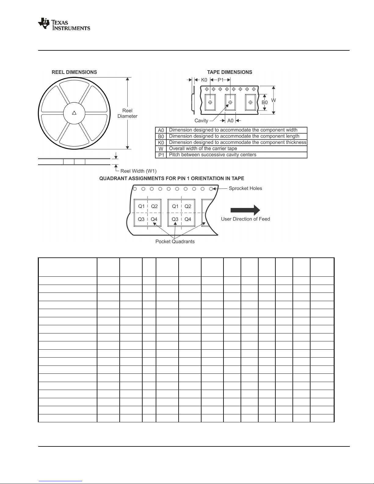
PACKAGE MATERIALS INFORMATION
www.ti.com 15-Oct-2015
TAPE AND REEL INFORMATION
*All dimensions are nominal
Device Package
MSP430G2203IPW20R TSSOP PW 20 2000 330.0 16.4 6.95 7.1 1.6 8.0 16.0 Q1
MSP430G2203IPW20R TSSOP PW 20 2000 330.0 16.4 6.95 7.1 1.6 8.0 16.0 Q1
MSP430G2203IPW28R TSSOP PW 28 2000 330.0 16.4 6.9 10.2 1.8 12.0 16.0 Q1
MSP430G2203IPW28R TSSOP PW 28 2000 330.0 16.4 6.9 10.2 1.8 12.0 16.0 Q1
MSP430G2203IRHB32R VQFN RHB 32 3000 330.0 12.4 5.3 5.3 1.1 8.0 12.0 Q2
MSP430G2233IPW20R TSSOP PW 20 2000 330.0 16.4 6.95 7.1 1.6 8.0 16.0 Q1
MSP430G2233IPW20R TSSOP PW 20 2000 330.0 16.4 6.95 7.1 1.6 8.0 16.0 Q1
MSP430G2233IPW28R TSSOP PW 28 2000 330.0 16.4 6.9 10.2 1.8 12.0 16.0 Q1
MSP430G2233IPW28R TSSOP PW 28 2000 330.0 16.4 6.9 10.2 1.8 12.0 16.0 Q1
MSP430G2233IRHB32R VQFN RHB 32 3000 330.0 12.4 5.3 5.3 1.1 8.0 12.0 Q2
MSP430G2233IRHB32T VQFN RHB 32 250 180.0 12.4 5.3 5.3 1.1 8.0 12.0 Q2
MSP430G2303IPW20R TSSOP PW 20 2000 330.0 16.4 6.95 7.1 1.6 8.0 16.0 Q1
MSP430G2303IPW28R TSSOP PW 28 2000 330.0 16.4 6.9 10.2 1.8 12.0 16.0 Q1
MSP430G2303IPW28R TSSOP PW 28 2000 330.0 16.4 6.9 10.2 1.8 12.0 16.0 Q1
MSP430G2303IRHB32R VQFN RHB 32 3000 330.0 12.4 5.3 5.3 1.1 8.0 12.0 Q2
MSP430G2303IRHB32T VQFN RHB 32 250 180.0 12.4 5.3 5.3 1.1 8.0 12.0 Q2
MSP430G2333IPW20R TSSOP PW 20 2000 330.0 16.4 6.95 7.1 1.6 8.0 16.0 Q1
MSP430G2333IPW28R TSSOP PW 28 2000 330.0 16.4 6.9 10.2 1.8 12.0 16.0 Q1
Type
Package
Drawing
Pins SPQ Reel
Diameter
(mm)
Reel
Width
W1 (mm)
A0
(mm)B0(mm)K0(mm)P1(mm)W(mm)
Quadrant
Pin1
Pack Materials-Page 1
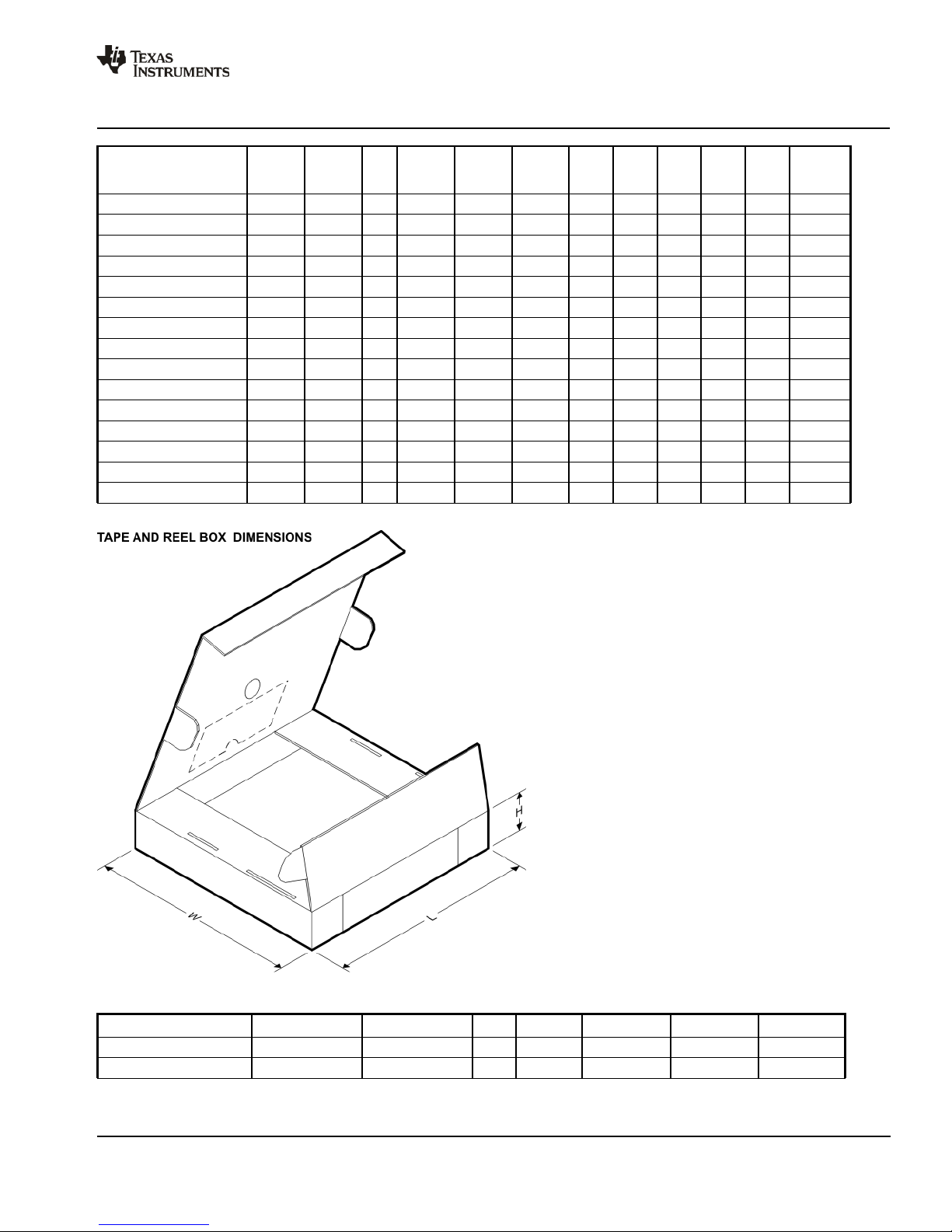
PACKAGE MATERIALS INFORMATION
www.ti.com 15-Oct-2015
Device Package
MSP430G2333IRHB32R VQFN RHB 32 3000 330.0 12.4 5.3 5.3 1.1 8.0 12.0 Q2
MSP430G2333IRHB32T VQFN RHB 32 250 180.0 12.4 5.3 5.3 1.1 8.0 12.0 Q2
MSP430G2403IPW20R TSSOP PW 20 2000 330.0 16.4 6.95 7.1 1.6 8.0 16.0 Q1
MSP430G2403IPW28R TSSOP PW 28 2000 330.0 16.4 6.9 10.2 1.8 12.0 16.0 Q1
MSP430G2403IRHB32R VQFN RHB 32 3000 330.0 12.4 5.3 5.3 1.1 8.0 12.0 Q2
MSP430G2403IRHB32T VQFN RHB 32 250 180.0 12.4 5.3 5.3 1.1 8.0 12.0 Q2
MSP430G2433IPW20R TSSOP PW 20 2000 330.0 16.4 6.95 7.1 1.6 8.0 16.0 Q1
MSP430G2433IPW28R TSSOP PW 28 2000 330.0 16.4 6.9 10.2 1.8 12.0 16.0 Q1
MSP430G2433IRHB32R VQFN RHB 32 3000 330.0 12.4 5.3 5.3 1.1 8.0 12.0 Q2
MSP430G2433IRHB32T VQFN RHB 32 250 180.0 12.4 5.3 5.3 1.1 8.0 12.0 Q2
MSP430G2533IPW20R TSSOP PW 20 2000 330.0 16.4 6.95 7.1 1.6 8.0 16.0 Q1
MSP430G2533IPW28R TSSOP PW 28 2000 330.0 16.4 6.9 10.2 1.8 12.0 16.0 Q1
MSP430G2533IPW28R TSSOP PW 28 2000 330.0 16.4 6.9 10.2 1.8 12.0 16.0 Q1
MSP430G2533IRHB32R VQFN RHB 32 3000 330.0 12.4 5.3 5.3 1.1 8.0 12.0 Q2
MSP430G2533IRHB32T VQFN RHB 32 250 180.0 12.4 5.3 5.3 1.1 8.0 12.0 Q2
Type
Package
Drawing
Pins SPQ Reel
Diameter
(mm)
Reel
Width
W1 (mm)
A0
(mm)B0(mm)K0(mm)P1(mm)W(mm)
Pin1
Quadrant
*All dimensions are nominal
Device Package Type Package Drawing Pins SPQ Length (mm) Width (mm) Height (mm)
MSP430G2203IPW20R TSSOP PW 20 2000 367.0 367.0 38.0
MSP430G2203IPW20R TSSOP PW 20 2000 367.0 367.0 38.0
Pack Materials-Page 2
PACKAGE MATERIALS INFORMATION
www.ti.com 15-Oct-2015
Device Package Type Package Drawing Pins SPQ Length (mm) Width (mm) Height (mm)
MSP430G2203IPW28R TSSOP PW 28 2000 367.0 367.0 38.0
MSP430G2203IPW28R TSSOP PW 28 2000 367.0 367.0 38.0
MSP430G2203IRHB32R VQFN RHB 32 3000 367.0 367.0 35.0
MSP430G2233IPW20R TSSOP PW 20 2000 367.0 367.0 38.0
MSP430G2233IPW20R TSSOP PW 20 2000 367.0 367.0 38.0
MSP430G2233IPW28R TSSOP PW 28 2000 367.0 367.0 38.0
MSP430G2233IPW28R TSSOP PW 28 2000 367.0 367.0 38.0
MSP430G2233IRHB32R VQFN RHB 32 3000 367.0 367.0 35.0
MSP430G2233IRHB32T VQFN RHB 32 250 210.0 185.0 35.0
MSP430G2303IPW20R TSSOP PW 20 2000 367.0 367.0 38.0
MSP430G2303IPW28R TSSOP PW 28 2000 367.0 367.0 38.0
MSP430G2303IPW28R TSSOP PW 28 2000 367.0 367.0 38.0
MSP430G2303IRHB32R VQFN RHB 32 3000 367.0 367.0 35.0
MSP430G2303IRHB32T VQFN RHB 32 250 210.0 185.0 35.0
MSP430G2333IPW20R TSSOP PW 20 2000 367.0 367.0 38.0
MSP430G2333IPW28R TSSOP PW 28 2000 367.0 367.0 38.0
MSP430G2333IRHB32R VQFN RHB 32 3000 367.0 367.0 35.0
MSP430G2333IRHB32T VQFN RHB 32 250 210.0 185.0 35.0
MSP430G2403IPW20R TSSOP PW 20 2000 367.0 367.0 38.0
MSP430G2403IPW28R TSSOP PW 28 2000 367.0 367.0 38.0
MSP430G2403IRHB32R VQFN RHB 32 3000 367.0 367.0 35.0
MSP430G2403IRHB32T VQFN RHB 32 250 210.0 185.0 35.0
MSP430G2433IPW20R TSSOP PW 20 2000 367.0 367.0 38.0
MSP430G2433IPW28R TSSOP PW 28 2000 367.0 367.0 38.0
MSP430G2433IRHB32R VQFN RHB 32 3000 367.0 367.0 35.0
MSP430G2433IRHB32T VQFN RHB 32 250 210.0 185.0 35.0
MSP430G2533IPW20R TSSOP PW 20 2000 367.0 367.0 38.0
MSP430G2533IPW28R TSSOP PW 28 2000 367.0 367.0 38.0
MSP430G2533IPW28R TSSOP PW 28 2000 367.0 367.0 38.0
MSP430G2533IRHB32R VQFN RHB 32 3000 367.0 367.0 35.0
MSP430G2533IRHB32T VQFN RHB 32 250 210.0 185.0 35.0
Pack Materials-Page 3
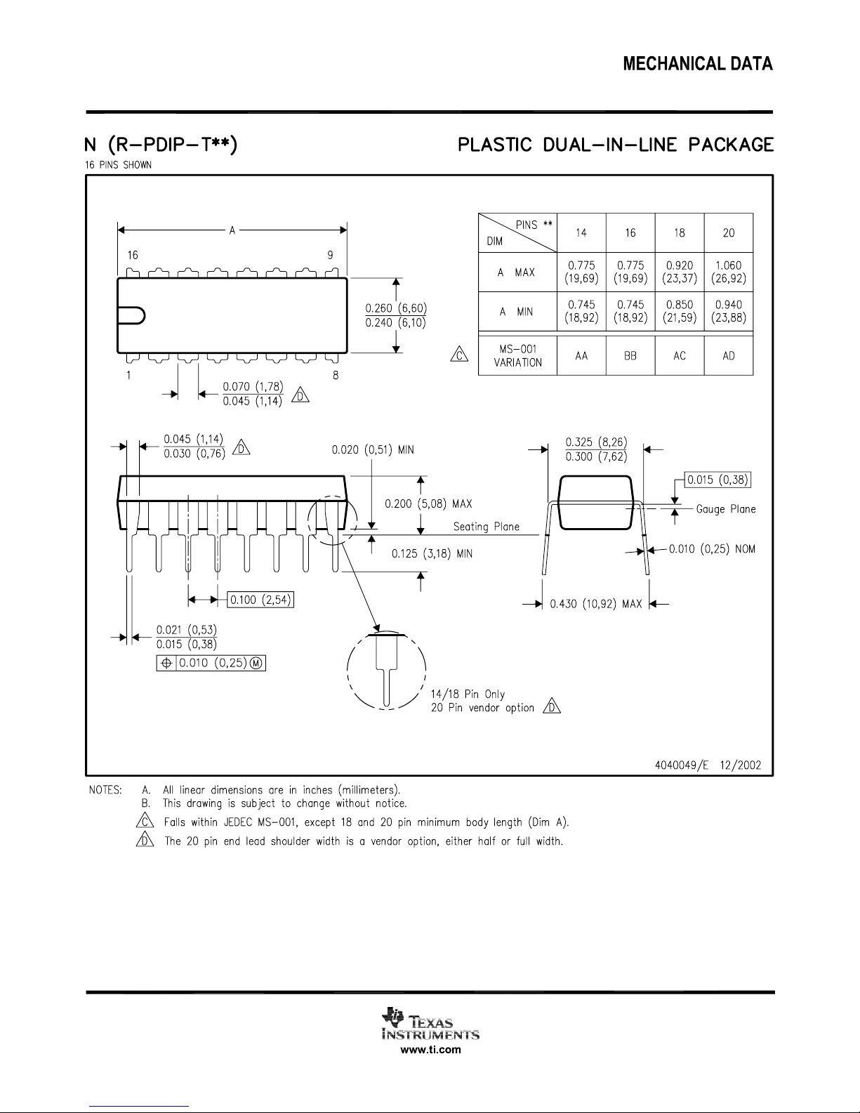


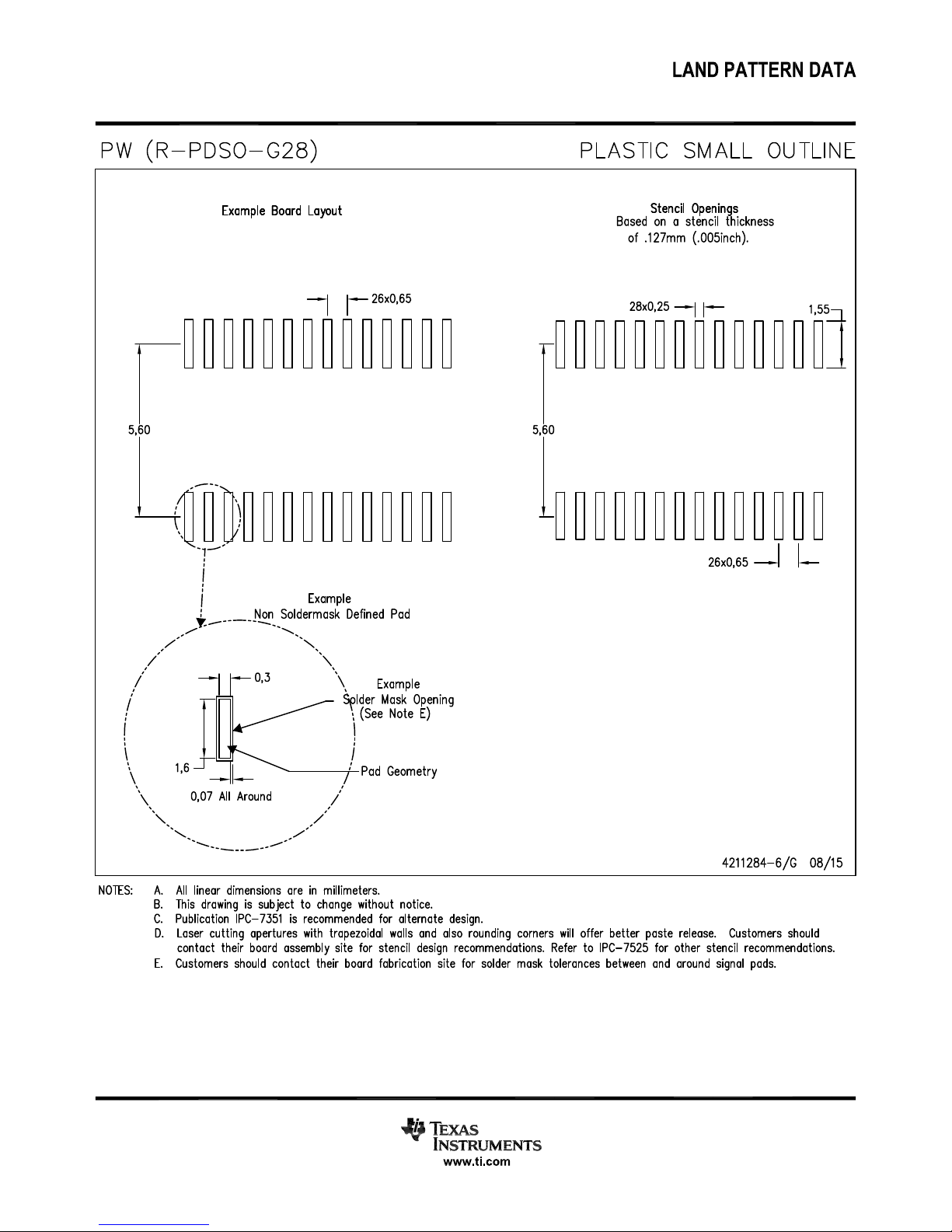
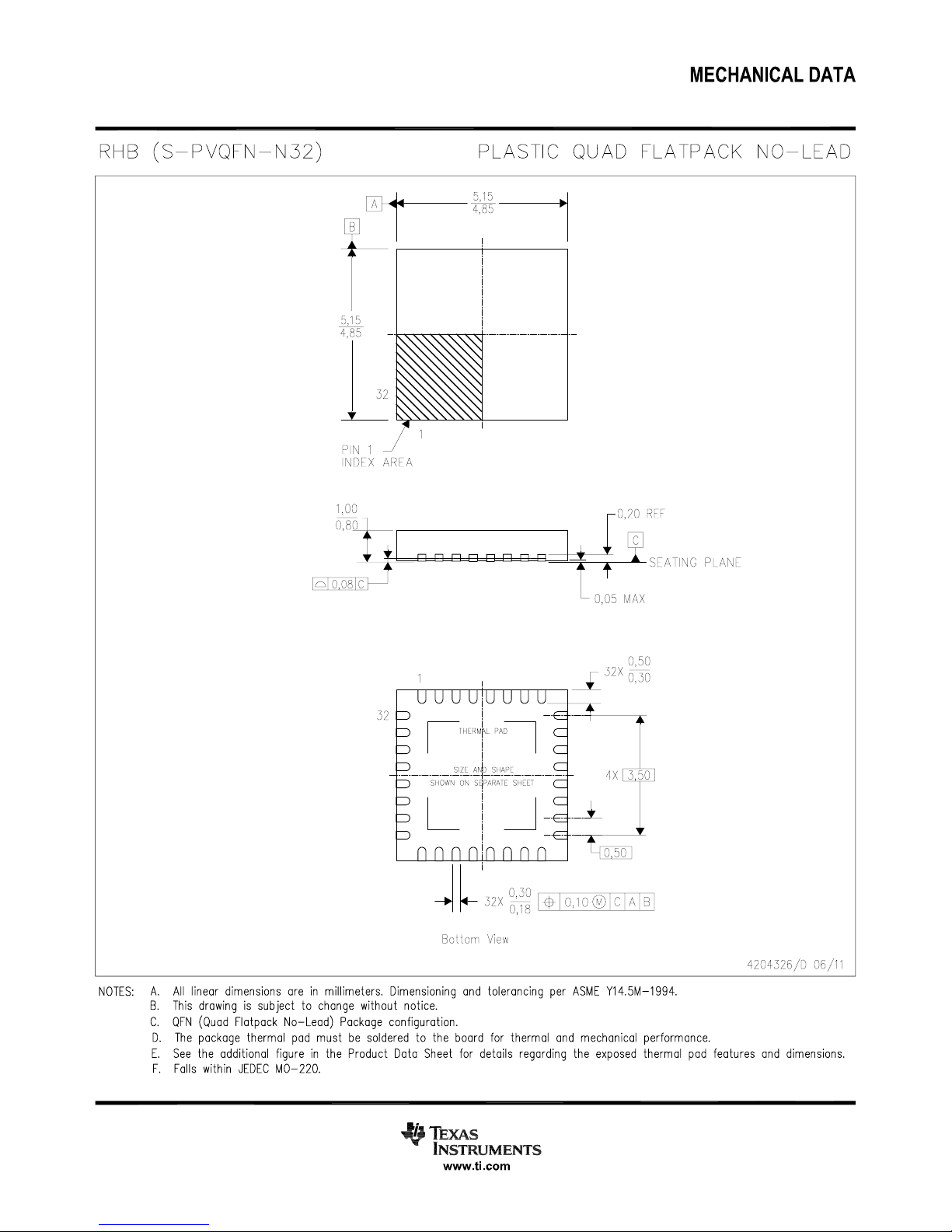


PACKAGE OUTLINE
PIN 1 INDEX AREA
0.9 MAX
0.05
0.00
28X 0.5
SCALE 3.000
VQFN - 0.9 mm max heightRHB0032N
PLASTIC QUAD FLATPACK - NO LEAD
A
9
8
5.1
4.9
2X 3.5
3.45 0.1
16
B
5.1
4.9
EXPOSED
THERMAL PAD
17
C
SEATING PLANE
0.08 C
0.05
SECTION A-A
A-A 30.000
TYPICAL
0.08
(0.2) TYP
2X
3.5
1
PIN 1 ID
(OPTIONAL)
32
NOTES:
1. All linear dimensions are in millimeters. Any dimensions in parenthesis are for reference only. Dimensioning and tolerancing
per ASME Y14.5M.
2. This drawing is subject to change without notice.
3. The package thermal pad must be soldered to the printed circuit board for thermal and mechanical performance.
33
SYMM
25
0.5
32X
0.3
www.ti.com
24
AA
SYMM
0.3
32X
0.2
0.1 C A B
0.05 C
4222893/A 04/2016

32X (0.6)
32
EXAMPLE BOARD LAYOUT
VQFN - 0.9 mm max heightRHB0032N
PLASTIC QUAD FLATPACK - NO LEAD
( 3.45)
SYMM
25
32X (0.25)
28X (0.5)
( ) TYP
0.2
(R )
0.05
TYP
VIA
1
33
8
9
(4.8)
(1.475)
16
24
(1.475)
SYMM
(4.8)
17
LAND PATTERN EXAMPLE
SCALE:18X
0.07 MAX
ALL AROUND
NON SOLDER MASK
DEFINED
(PREFERRED)
NOTES: (continued)
4. This package is designed to be soldered to a thermal pad on the board. For more information, see Texas Instruments literature
number SLUA271 (www.ti.com/lit/slua271).
5. Vias are optional depending on application, refer to device data sheet. If any vias are implemented, refer to their locations shown
on this view. It is recommended that vias under paste be filled, plugged or tented.
METAL
SOLDER MASK
OPENING
SOLDER MASK DETAILS
www.ti.com
0.07 MIN
ALL AROUND
SOLDER MASK
OPENING
METAL UNDER
SOLDER MASK
SOLDER MASK
DEFINED
4222893/A 04/2016

(R ) TYP0.05
32X (0.6)
32
EXAMPLE STENCIL DESIGN
VQFN - 0.9 mm max heightRHB0032N
PLASTIC QUAD FLATPACK - NO LEAD
4X ( 1.49)
(0.845)
25
32X (0.25)
28X (0.5)
METAL
TYP
1
33
8
9
SYMM
16
24
(0.845)
SYMM
(4.8)
17
75% PRINTED SOLDER COVERAGE BY AREA UNDER PACKAGE
NOTES: (continued)
6. Laser cutting apertures with trapezoidal walls and rounded corners may offer better paste release. IPC-7525 may have alternate
design recommendations.
(4.8)
SOLDER PASTE EXAMPLE
BASED ON 0.125 mm THICK STENCIL
EXPOSED PAD 33:
SCALE:20X
4222893/A 04/2016
www.ti.com


IMPORTANT NOTICE
Texas Instruments Incorporated and its subsidiaries (TI) reserve the right to make corrections, enhancements, improvements and other
changes to its semiconductor products and services per JESD46, latest issue, and to discontinue any product or service per JESD48, latest
issue. Buyers should obtain the latest relevant information before placing orders and should verify that such information is current and
complete. All semiconductor products (also referred to herein as “components”) are sold subject to TI’s terms and conditions of sale
supplied at the time of order acknowledgment.
TI warrants performance of its components to the specifications applicable at the time of sale, in accordance with the warranty in TI’s terms
and conditions of sale of semiconductor products. Testing and other quality control techniques are used to the extent TI deems necessary
to support this warranty. Except where mandated by applicable law, testing of all parameters of each component is not necessarily
performed.
TI assumes no liability for applications assistance or the design of Buyers’ products. Buyers are responsible for their products and
applications using TI components. To minimize the risks associated with Buyers’ products and applications, Buyers should provide
adequate design and operating safeguards.
TI does not warrant or represent that any license, either express or implied, is granted under any patent right, copyright, mask work right, or
other intellectual property right relating to any combination, machine, or process in which TI components or services are used. Information
published by TI regarding third-party products or services does not constitute a license to use such products or services or a warranty or
endorsement thereof. Use of such information may require a license from a third party under the patents or other intellectual property of the
third party, or a license from TI under the patents or other intellectual property of TI.
Reproduction of significant portions of TI information in TI data books or data sheets is permissible only if reproduction is without alteration
and is accompanied by all associated warranties, conditions, limitations, and notices. TI is not responsible or liable for such altered
documentation. Information of third parties may be subject to additional restrictions.
Resale of TI components or services with statements different from or beyond the parameters stated by TI for that component or service
voids all express and any implied warranties for the associated TI component or service and is an unfair and deceptive business practice.
TI is not responsible or liable for any such statements.
Buyer acknowledges and agrees that it is solely responsible for compliance with all legal, regulatory and safety-related requirements
concerning its products, and any use of TI components in its applications, notwithstanding any applications-related information or support
that may be provided by TI. Buyer represents and agrees that it has all the necessary expertise to create and implement safeguards which
anticipate dangerous consequences of failures, monitor failures and their consequences, lessen the likelihood of failures that might cause
harm and take appropriate remedial actions. Buyer will fully indemnify TI and its representatives against any damages arising out of the use
of any TI components in safety-critical applications.
In some cases, TI components may be promoted specifically to facilitate safety-related applications. With such components, TI’s goal is to
help enable customers to design and create their own end-product solutions that meet applicable functional safety standards and
requirements. Nonetheless, such components are subject to these terms.
No TI components are authorized for use in FDA Class III (or similar life-critical medical equipment) unless authorized officers of the parties
have executed a special agreement specifically governing such use.
Only those TI components which TI has specifically designated as military grade or “enhanced plastic” are designed and intended for use in
military/aerospace applications or environments. Buyer acknowledges and agrees that any military or aerospace use of TI components
which have not been so designated is solely at the Buyer's risk, and that Buyer is solely responsible for compliance with all legal and
regulatory requirements in connection with such use.
TI has specifically designated certain components as meeting ISO/TS16949 requirements, mainly for automotive use. In any case of use of
non-designated products, TI will not be responsible for any failure to meet ISO/TS16949.
Products Applications
Audio www.ti.com/audio Automotive and Transportation www.ti.com/automotive
Amplifiers amplifier.ti.com Communications and Telecom www.ti.com/communications
Data Converters dataconverter.ti.com Computers and Peripherals www.ti.com/computers
DLP® Products www.dlp.com Consumer Electronics www.ti.com/consumer-apps
DSP dsp.ti.com Energy and Lighting www.ti.com/energy
Clocks and Timers www.ti.com/clocks Industrial www.ti.com/industrial
Interface interface.ti.com Medical www.ti.com/medical
Logic logic.ti.com Security www.ti.com/security
Power Mgmt power.ti.com Space, Avionics and Defense www.ti.com/space-avionics-defense
Microcontrollers microcontroller.ti.com Video and Imaging www.ti.com/video
RFID www.ti-rfid.com
OMAP Applications Processors www.ti.com/omap TI E2E Community e2e.ti.com
Wireless Connectivity www.ti.com/wirelessconnectivity
Mailing Address: Texas Instruments, Post Office Box 655303, Dallas, Texas 75265
Copyright © 2016, Texas Instruments Incorporated
 Loading...