Texas Instruments LT1030CN, LT1030CDR, LT1030CD Datasheet

LT1030C
QUADRUPLE LOW-POWER LINE DRIVER
SLLS048F – APRIL 1989 – REVISED APRIL 1998
1
POST OFFICE BOX 655303 • DALLAS, TEXAS 75265
D
Low Supply Voltage . . . ±5 V to ±15 V
D
Supply Current...500 µA Typical
D
Zero Supply Current When Shut Down
D
Outputs Can Be Driven ±30 V
D
Output Open When Off (3-State)
D
10-mA Output Drive
D
Outputs of Several Devices Can Be
Connected in Parallel
D
Meets or Exceeds the Requirements of
ANSI EIA/TIA-232-F Specifications
D
Designed to Be Interchangeable With
Linear Technology LT1030
description
The L T1030C is an EIA/TIA-232-F line driver that operates over a ±5-V to ±15-V supply-voltage range on low
supply current. The device can be shut down to zero supply current. Current limiting fully protects the outputs
from externally applied voltages of ±30 V . Since the output swings to within 200 mV of the positive supply and
to within 1 V of the negative supply, supply-voltage requirements are minimized.
A major advantage of the L T1030C is the high-impedance output state when the device is off or powered down.
This feature allows several different drivers on the same bus.
The device can be used as an EIA/TIA-232-F driver, micropower interface, or level translator, among others.
The LT1030C is characterized for operation from 0°C to 70°C.
AVAILABLE OPTIONS
PACKAGE
SMALL OUTLINE
(D)
PLASTIC DIP
(N)
LT1030CD LT1030CN
The D package is available taped and reeled.
Add the suffix R to the device type (i.e.,
LT1030CDR).
Copyright 1998, Texas Instruments Incorporated
PRODUCTION DATA information is current as of publication date.
Products conform to specifications per the terms of Texas Instruments
standard warranty. Production processing does not necessarily include
testing of all parameters.
Please be aware that an important notice concerning availability, standard warranty, and use in critical applications of
Texas Instruments semiconductor products and disclaimers thereto appears at the end of this data sheet.
1
2
3
4
5
6
7
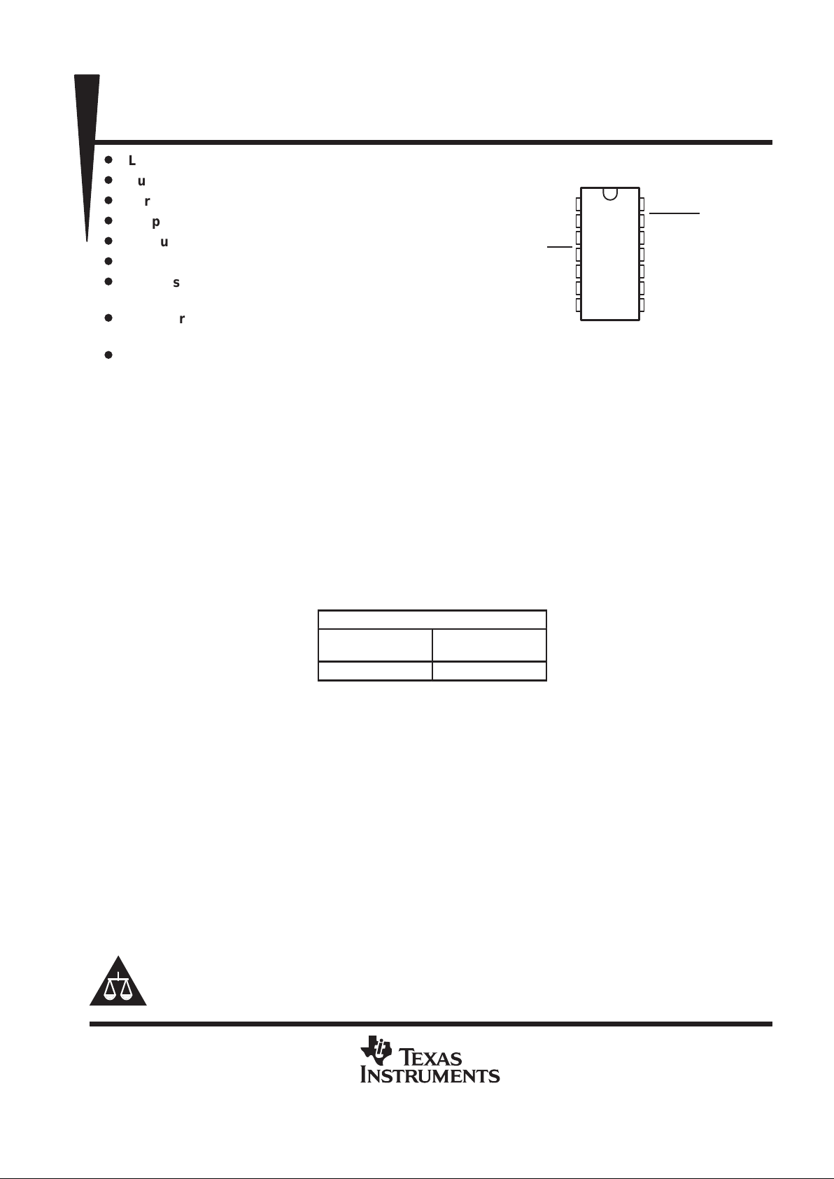
14
13
12
11
10
9
8
V
CC–
IN1
OUT1
ON/OFF
IN2
OUT2
GND
V
CC+
STROBE
IN4
OUT4
NC
IN3
OUT3
D OR N PACKAGE
(TOP VIEW)
NC – No internal connection

LT1030C
QUADRUPLE LOW-POWER LINE DRIVER
SLLS048F – APRIL 1989 – REVISED APRIL 1998
2
POST OFFICE BOX 655303 • DALLAS, TEXAS 75265
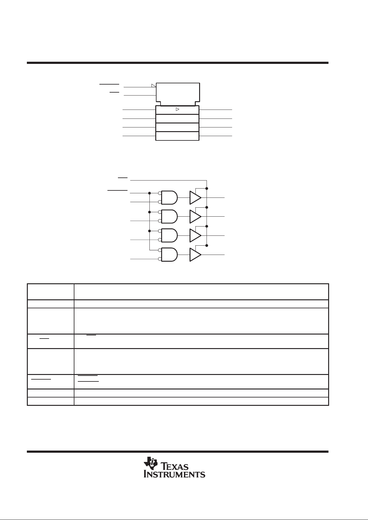
logic symbol
†
STROBE
ON/OFF
G1
13
EN
4
†
This symbol is in accordance with ANSI/IEEE Std 91-1984 and IEC Publication 617-12.
OUT1
3
OUT2
6
OUT3
8
OUT4
11
1
2
IN1
5
IN2
9
IN3
12
IN4
logic diagram
OUT1
ON/OFF
STROBE
IN1
3
13
4
2
OUT2
IN2
6
5
OUT3
IN3
8
9
OUT4
IN4
11
12
Terminal Functions
TERMINAL
NAME NO.
DESCRIPTION
GND 7 Ground terminal
IN1
IN2
IN3
IN4
2
5
9
12
Logic inputs. INx operate properly on TTL or CMOS levels. Output valid from VI = V
CC–
+ 2 V to 15 V . Connect to 5 V
when not used.
ON/OFF
4
ON/OFF shuts down the entire circuit. It cannot be left open. For normally on operation, connect between 5 V and 10 V .
If VIL is at or near 0.8 V, significant settling time may be required.
OUT1
OUT2
OUT3
OUT4
3
6
8
11
Line driver outputs
STROBE
13
STROBE forces all outputs low. Drive with 3 V. Strobe terminal input impedance is approximately 2 k Ω to GND. Leave
STROBE
open when not used.
V
CC+
14 Positive supply
V
CC–
1 Negative supply

LT1030C
QUADRUPLE LOW-POWER LINE DRIVER
SLLS048F – APRIL 1989 – REVISED APRIL 1998
3
POST OFFICE BOX 655303 • DALLAS, TEXAS 75265
absolute maximum ratings over operating free-air temperature range (unless otherwise noted)
†
Supply voltage range, V
CC+
(see Note 1) 0 V to 15 V. . . . . . . . . . . . . . . . . . . . . . . . . . . . . . . . . . . . . . . . . . . . . . .
Supply voltage range, V
CC–
0 V to –15 V. . . . . . . . . . . . . . . . . . . . . . . . . . . . . . . . . . . . . . . . . . . . . . . . . . . . . . . . . .
Input voltage range, logic inputs, V
I
V
CC–
to 25 V. . . . . . . . . . . . . . . . . . . . . . . . . . . . . . . . . . . . . . . . . . . . . . . . . .
Input voltage range at ON/OFF
, VI 0 V to 12 V. . . . . . . . . . . . . . . . . . . . . . . . . . . . . . . . . . . . . . . . . . . . . . . . . . . . .
Output voltage range, V
O
(any output) V
CC+
– 30 V to V
CC–
+ 30 V. . . . . . . . . . . . . . . . . . . . . . . . . . . . . . . . . .
Duration of output short circuit to ±30 V at (or below) 25°C (see Note 2) Unlimited. . . . . . . . . . . . . . . . . . . . . . .
Package thermal impedance, θ
JA
(see Note 3): D package 127°C/W. . . . . . . . . . . . . . . . . . . . . . . . . . . . . . . . . .
N package 78°C/W. . . . . . . . . . . . . . . . . . . . . . . . . . . . . . . . . . .
Storage temperature range, T
stg
–65°C to 150°C. . . . . . . . . . . . . . . . . . . . . . . . . . . . . . . . . . . . . . . . . . . . . . . . . . .
Lead temperature 1,6 mm (1/16 inch) from case for 10 seconds 260°C. . . . . . . . . . . . . . . . . . . . . . . . . . . . . . .
†
Stresses beyond those listed under “absolute maximum ratings” may cause permanent damage to the device. These are stress ratings only, and
functional operation of the device at these or any other conditions beyond those indicated under “recommended operating conditions” is not
implied. Exposure to absolute-maximum-rated conditions for extended periods may affect device reliability.
NOTES: 1. All voltage values, except differential voltages, are with respect to GND.
2. The output may be shorted to either supply. Temperature and/or supply voltages must be limited to ensure that the maximum
dissipation rating is not exceeded.
3. The package thermal impedance is calculated in accordance with JESD 51, except for through-hole packages, which use a trace
length of zero.
recommended operating conditions
MIN MAX UNIT
Supply voltage, V
CC+
5 15 V
Supply voltage, V
CC–
–5 –15 V
High-level input voltage, VIH (see Note 4) 2 15 V
Low-level input voltage, VIL (see Note 4) 0.8 V
Operating free-air temperature, T
A
0 70 °C
NOTE 4: These VIH and VIL specifications apply only for inputs IN1–IN4. For operating levels for ON/OFF, see Figure 2.
electrical characteristics over operating free-air temperature range, V
CC±
= ±5 V to ±15 V (unless
otherwise noted)
PARAMETER TEST CONDITIONS MIN TYP
‡
MAX UNIT
V
OM+
Maximum positive peak output voltage swing IO = –2 mA, TA = 25°C V
CC+
–0.3 V
CC+
–0.1 V
V
OM–
Maximum negative peak output voltage swing IO = 2 mA, TA = 25°C V
CC–
+0.9 V
CC–
+1.4 V
I
IH
High-level input current VI ≥ 2 V, TA = 25°C 2 20 µA
I
IL
Low-level input current VI ≤ 0.8 V, TA = 25°C –10 –20 µA
VI = 0 –0.1 –10
II
I
nput current,
ON/OFF
VI = 5 V 30 65
µ
A
I
O
Output current TA = 25°C 5 12 mA
I
OZ
Off-state output current
VO = ±15 V , TA = 25°C,
ON/OFF
at 0.4 V
±2 ±100 µA
I
CC
Supply current (all outputs low) VI ≥ at 2.4 V, IO = 0 500 1000 µA
pp
ON/OFF at 0.4 V 10
I
CC(off)
Off-state supply current
ON/OFF at 0.1 V 10 150
µ
A
‡
All typical values are at V
CC±
= ±12 V , TA = 25°C.
 Loading...