

查询5962-89677012A供应商
LT1014, LT1014A, LT1014D
QUAD PRECISION OPERATIONAL AMPLIFIERS
SLOS039C – JULY 1989 – REVISED SEPTEMBER 1999
D
Single-Supply Operation:
Input Voltage Range Extends to Ground,
and Output Swings to Ground While
Sinking Current
D
Input Offset Voltage 300 µV Max at 25°C for
LT1014
D
Offset Voltage Temperature Coefficient
2.5 µV/°C Max for LT1014
D
Input Offset Current 1.5 nA Max at 25°C for
LT1014
D
High Gain 1.2 V/µV Min (R
Min (R
D
Low Supply Current 2.2 mA Max at 25°C for
= 600 Ω) for LT1014
L
= 2 kΩ), 0.5 V/µV
L
LT 1014
D
Low Peak-to-Peak Noise Voltage
0.55 µV Typ
D
Low Current Noise 0.07 pA/√Hz Typ
description
The LT1014, LT1014A, and LT1014D are quad
precision operational amplifiers with 14-pin
industry-standard configuration. They feature low
offset-voltage temperature coefficient, high gain,
low supply current, and low noise.
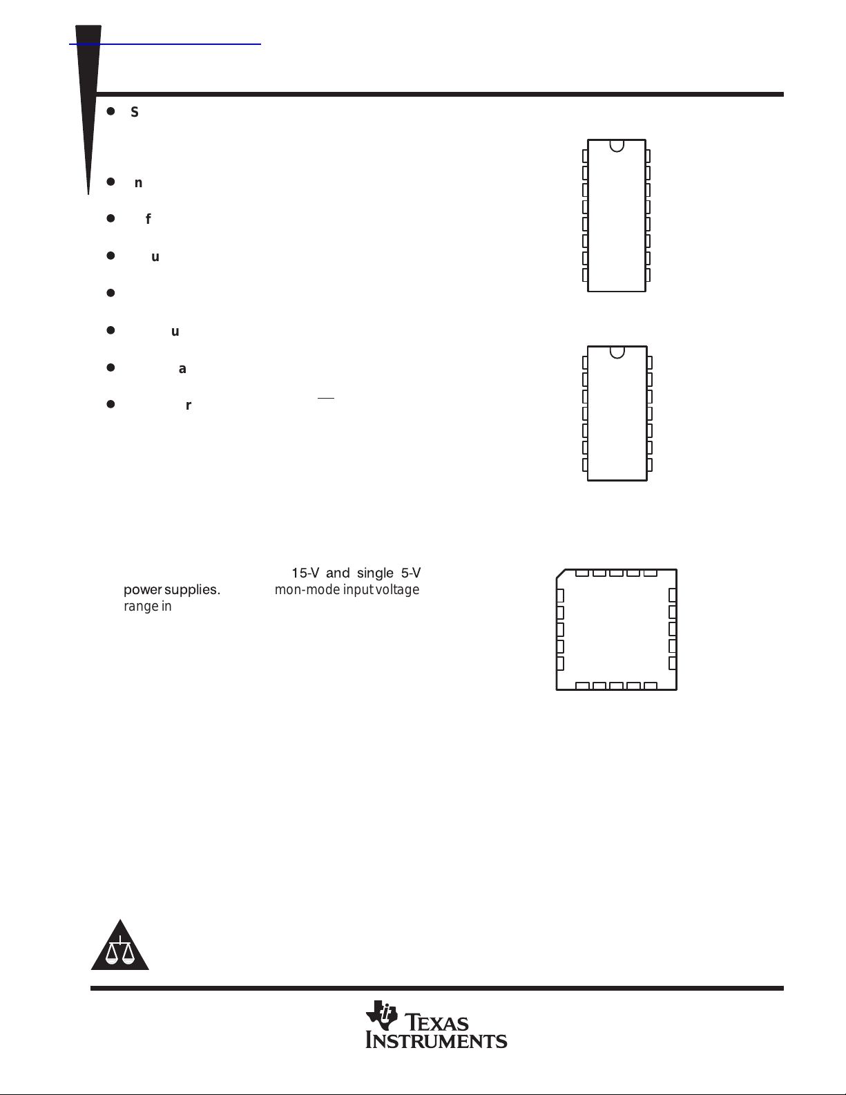
DW PACKAGE
(TOP VIEW)
1OUT
V
2OUT
1OUT
V
2OUT
1
1IN–
2
3
1IN+
4
CC+
5
2IN+
6
2IN–
7
8
NC
J OR N PACKAGE
(TOP VIEW)
1
1IN–
2
1IN+
3
4
CC+
2IN+
5
2IN–
6
7
FK PACKAGE
(TOP VIEW)
16
15
14
13
12
11
10
14
13
12
10
4OUT
4IN–
4IN+
V
/GND
CC–
3IN+
3IN–
3OUT
9
NC
4OUT
4IN–
4IN+
V
11
CC–
3IN+
3IN–
9
3OUT
8
The LT1014, LT1014A, and LT1014D can be
operated with both dual ±
powersupplies.
The common-mode input voltage
15ĆV and single 5ĆV
range includes ground, and the output voltage can
also swing to within a few milivolts of ground.
Crossover distortion is eliminated.
The LT1014C and LT1014 AC are characterized
for operation from 0°C to 70°C. The L T1014I and
1IN+
V
CC+
2IN+
NC
NC
1IN–
1OUT
NC
3212019
4
5
6
7
8
910111213
4IN–
4OUT
18
17
16
15
14
4IN+
NC
V
CC–
NC
3IN+
LT1014DI are characterized for operation from
–40°C to 105°C. The LT1014M, LT1014AM and
LT1014DM are characterized for operation over
the full military temperature range of –55°C to
2IN–
2OUTNC3OUT
NC – No internal connection
3IN–
125°C.
Please be aware that an important notice concerning availability, standard warranty, and use in critical applications of
Texas Instruments semiconductor products and disclaimers thereto appears at the end of this data sheet.
/GND
PRODUCTION DATA information is current as of publication date.
Products conform to specifications per the terms of Texas Instruments
standard warranty. Production processing does not necessarily include
testing of all parameters.
POST OFFICE BOX 655303 • DALLAS, TEXAS 75265
Copyright 1999, Texas Instruments Incorporated
1
LT1014, LT1014A, LT1014D
0°C to 70°C
µ
40°C to 105°C
µ
180 µV
LT1014AMFK
LT1014AMJ
µ
QUAD PRECISION OPERATIONAL AMPLIFIERS
SLOS039C – JULY 1989 – REVISED SEPTEMBER 1999
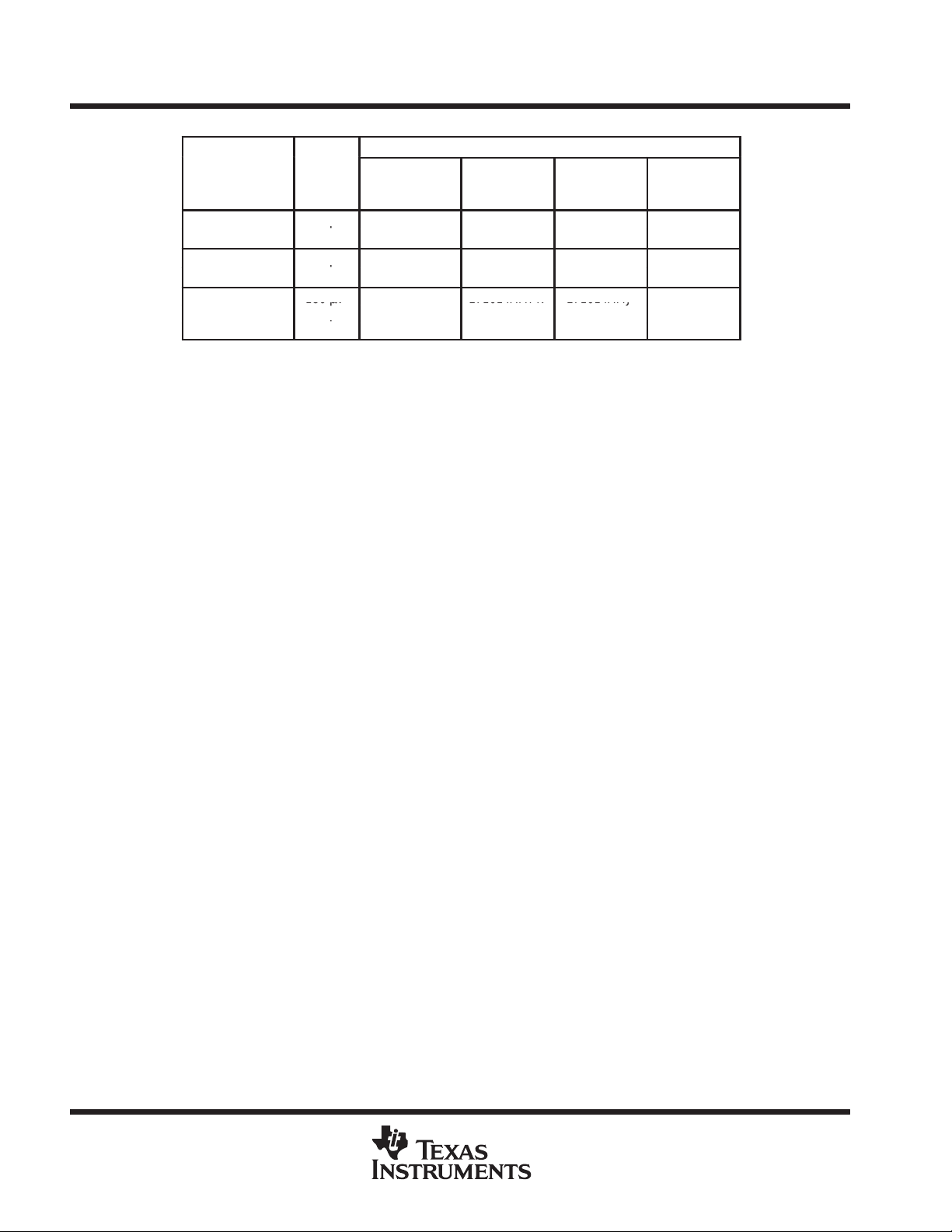
AVAILABLE OPTIONS
T
A
°
°
°
–
–55°C to 125°C
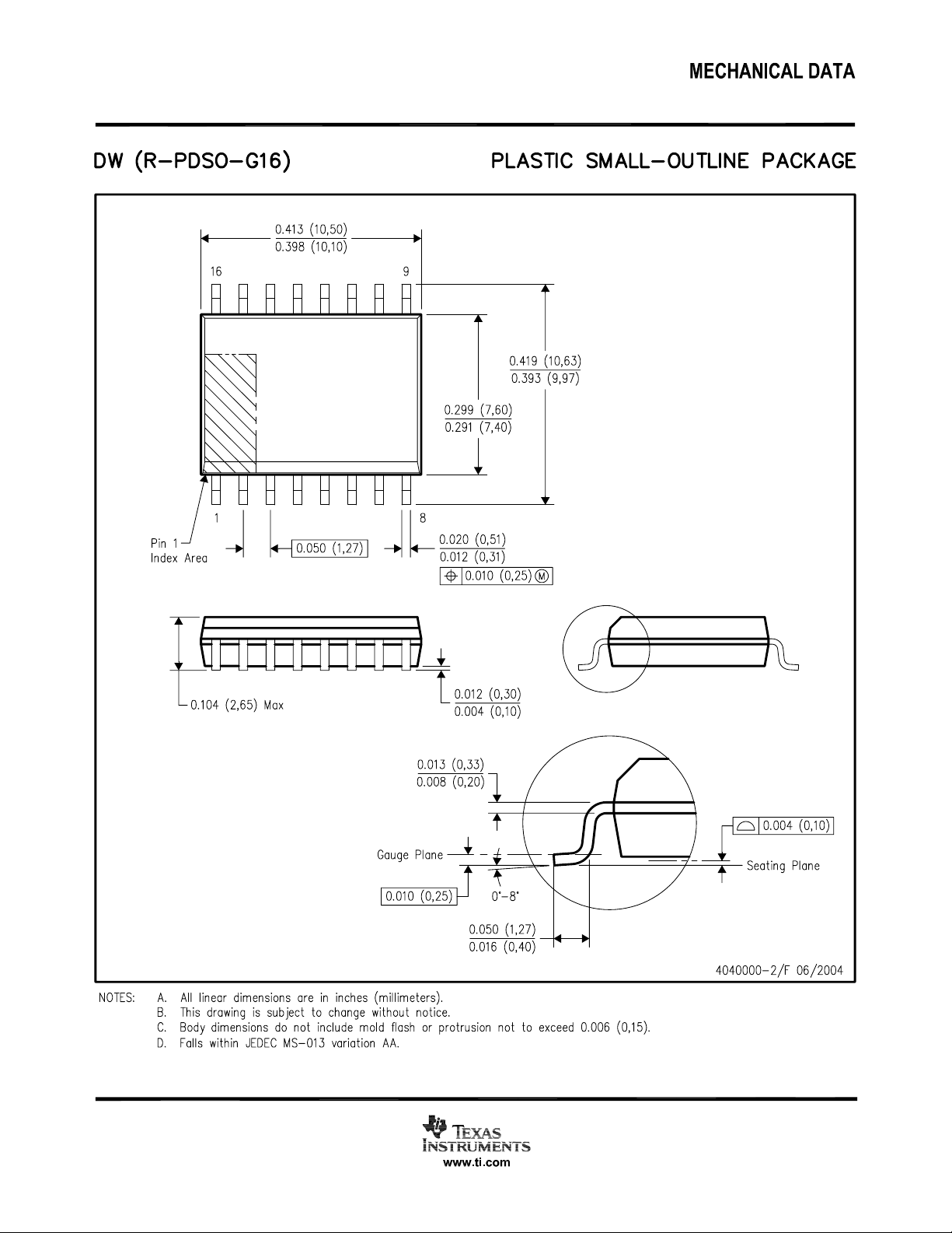
The DW package is available taped and reeled. Add the suffix R to the device type (e.g., L T1014DDWR).
VIO max
AT 25°C
300 µV — — — LT1014CN
800 µV LT1014DDW — — LT1014DN
300 µV — — — LT1014IN
°
800 µV LT1014DIDW — — LT1014DIN
180 µV — LT1014AMFK LT1014AMJ —
300 µV —
800 µV LT1014DMDW — — LT1014DMN
SMALL
OUTLINE
(DW)
PACKAGED DEVICES
CHIP
CARRIER
(FK)
LT1014MFK
CERAMIC
LT1014MJ LT1014MN
DIP
(J)
PLASTIC
DIP
(N)
2
POST OFFICE BOX 655303 • DALLAS, TEXAS 75265
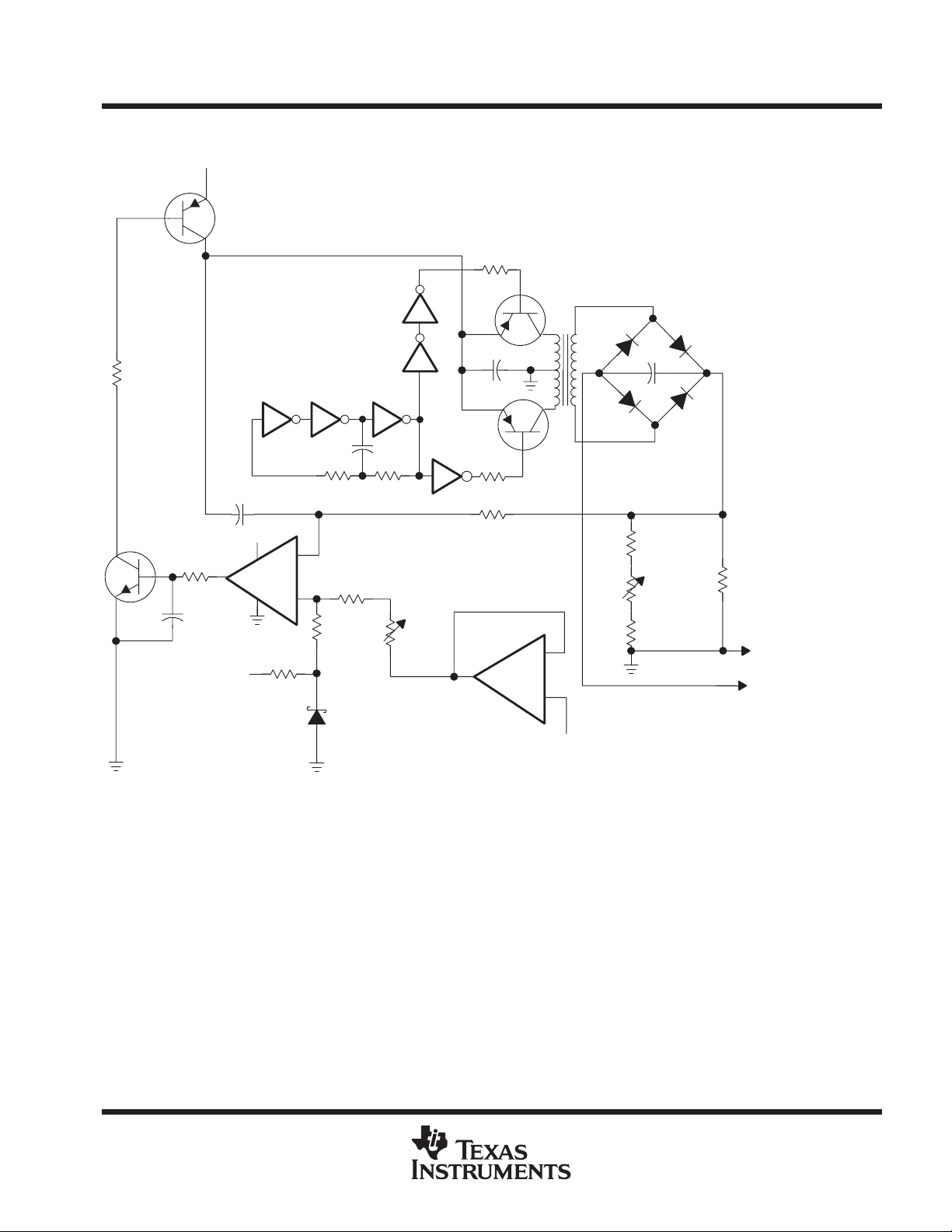
schematic (each amplifier)
LT1014, LT1014A, LT1014D
QUAD PRECISION OPERATIONAL AMPLIFIERS
SLOS039C – JULY 1989 – REVISED SEPTEMBER 1999
Q36
Q35
Q30
Q41
J1
Q37
Q33
Q26
Q25
Ωk3.9
Q38
Ωk14
OUT
Ω18
Ωk2.4
2.5 pF
21 pF
Q39
Q40
Q31
4 pF
Q18
Q10
Q34
Ωk2
Q19
10 pF
Q23
Q17
10 pF
Q24
Q20
Ω600
Ωk42
Ω30
Ωk2
Ωk1.3
Ωk2
V
CC+
Ωk9 Ωk9 Ωk1.6 Ωk1.6 Ωk1.6 Ω100 Ωk1 Ω800
Q5
Q6 Q13 Q16 Q14 Q15 Q32
Q3
Q4
Q27
Q1
Ω400
IN–
Q28
Q2
Q21
Ω400
IN+
Q12
Q22
Q29
Q8
Q7
Q11
Q9
Ωk5 Ωk5
75 pF
CC–
Component values are nominal.
V
POST OFFICE BOX 655303 • DALLAS, TEXAS 75265
3
LT1014, LT1014A, LT1014D
QUAD PRECISION OPERATIONAL AMPLIFIERS
SLOS039C – JULY 1989 – REVISED SEPTEMBER 1999
absolute maximum ratings over operating free-air temperature range (unless otherwise noted)
Supply voltage (see Note 1): V
Differential input voltage (see Note 2) ±30 V. . . . . . . . . . . . . . . . . . . . . . . . . . . . . . . . . . . . . . . . . . . . . . . . . . . . . . . .
Input voltage range, VI (any input) (see Note 1) V
Duration of short-circuit current at (or below) T
Continuous total power dissipation See Dissipation Rating Table. . . . . . . . . . . . . . . . . . . . . . . . . . . . . . . . . . . . .
Operating free-air temperature range, TA: LT1014C, LT1014DC –0°C to 70°C. . . . . . . . . . . . . . . . . . . . . . . . . .
Lead temperature 1,6 mm (1/16 inch) from case for 60 seconds: J package 300°C. . . . . . . . . . . . . . . . . . . . .
Lead temperature 1,6 mm (1/16 inch) from case for 10 seconds: DW or N package 260°C. . . . . . . . . . . . . . .
Case temperature for 60 seconds: FK package 260°C. . . . . . . . . . . . . . . . . . . . . . . . . . . . . . . . . . . . . . . . . . . . . .
Storage temperature range, T
†
Stresses beyond those listed under “absolute maximum ratings” may cause permanent damage to the device. These are stress ratings only, and
functional operation of the device at these or any other conditions beyond those indicated under “recommended operating conditions” is not
implied. Exposure to absolute-maximum-rated conditions for extended periods may affect device reliability.
NOTES: 1. All voltage values, except differential voltages, are with respect to the midpoint between V
2. Differential voltages are at the noninverting input with respect to the inverting input.
3. The output may be shorted to either supply.
PACKAGE
DW 1025 mV 8.2 mW/°C 656 mW 369 mW 205 mW
FK 1375 mV 11.0 mW/°C 880 mW 495 mW 275 mW
J 1375 mV 11.0 mW/°C 880 mW 495 mW 275 mW
N 1150 mV 9.2 mW/°C 736 mW 414 mW 230 mW
TA ≤ 25°C
POWER RATING
22 V. . . . . . . . . . . . . . . . . . . . . . . . . . . . . . . . . . . . . . . . . . . . . . . . . . . . . . . . . .
CC+
V
–22 V. . . . . . . . . . . . . . . . . . . . . . . . . . . . . . . . . . . . . . . . . . . . . . . . . . . . . . . . . .
CC–
. . . . . . . . . . . . . . . . . . . . . . . . . . . . . . . . . .
= 25°C (see Note 3) Unlimited. . . . . . . . . . . . . . . . . . . . . . . . .
A
CC–
LT1014I, LT1014DI –40°C to 105°C. . . . . . . . . . . . . . . . . . . . . . . . . .
LT1014M, LT1014AM, LT1014DM –55°C to 125°C. . . . . . . . . . . . .
–65°C to 150°C. . . . . . . . . . . . . . . . . . . . . . . . . . . . . . . . . . . . . . . . . . . . . . . . . . .
stg
and V
DISSIPATION RATING TABLE
DERATING FACTOR
ABOVE TA = 25°C
TA = 70°C
POWER RATING
CC+
TA = 105°C
POWER RATING
CC–.
TA = 125°C
POWER RATING
– 5 V to V
CC+
†
4
POST OFFICE BOX 655303 • DALLAS, TEXAS 75265
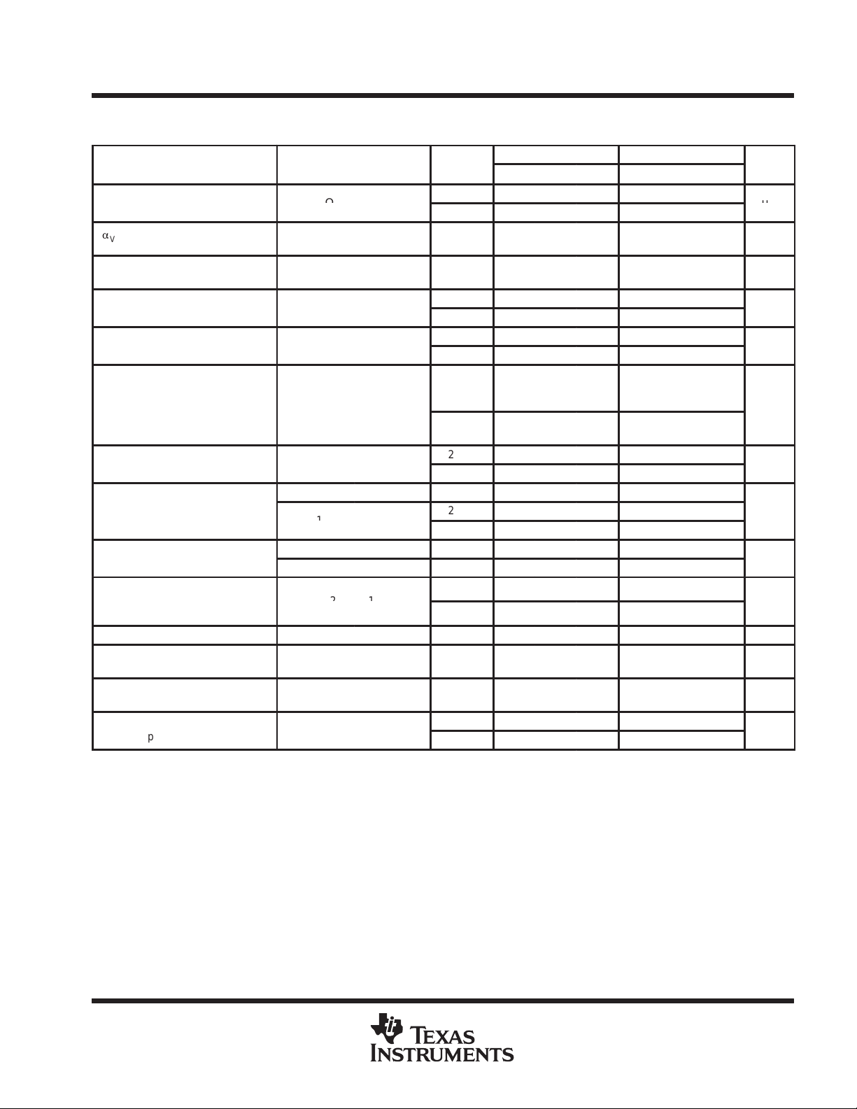
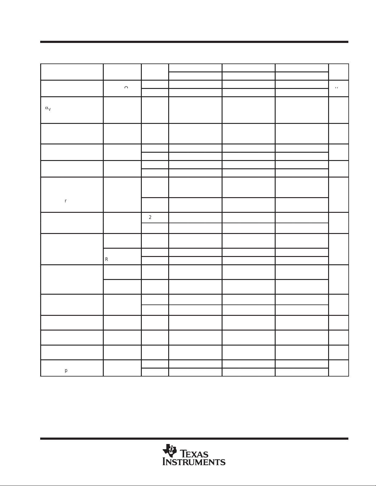
PARAMETER
TEST CONDITIONS
T
†
UNIT
VIOInput offset voltage
R
Ω
V
IIOInput offset current
nA
IIBInput bias current
nA
ICR
i
V
R
2 kΩ
V
voltage am lification
V
±10 V
R
kΩ
CMRR
dB
k
V
±18 V
dB
I
y
mA
LT1014, LT1014A, LT1014D
QUAD PRECISION OPERATIONAL AMPLIFIERS
SLOS039C – JULY 1989 – REVISED SEPTEMBER 1999
electrical characteristics at specified free-air temperature, V
noted)
p
a
V
A
r
id
r
ic
CC
†
Full range is 0°C to 70°C.
‡
All typical values are at TA = 25°C.
T emperature coeficient
V
IO
of input offset voltage
Long-term drift
of input offset voltage
p
p
Common-mode
p
nput voltage range
Maximum peak output
OM
voltage swing
Large-signal differential
VD
Common-mode
rejection ratio
Supply-voltage
rejection ratio
SVR
(∆VCC/∆VIO)
Channel separation VO = ±10 V, RL = 2 kΩ 25°C 120 137 120 137 dB
Differential
input resistance
Common-mode
input resistance
Supply current
per amplifier
p
A
= 50
S
=
L
VO = ±10 V, RL = 600 Ω 25°C 0.5 2 0.5 2
=
,
O
VIC = –15 V to 13.5 V 25°C 97 117 97 117
VIC = –15 V to 13 V
= ±2 V to
CC±
L
= 2
25°C 60 300 200 800
Full range 550 1000
Full range 0.4 2.5 0.7 5 µV/°C
25°C 0.5 0.5 µV/mo
25°C 0.15 1.5 0.15 1.5
Full range 2.8 2.8
25°C –12 –30 –12 –30
Full range –38 –38
25°C
Full range
25°C ±12.5 ±14 ±12.5 ±14
Full range ±12 ±12
25°C 1.2 8 1.2 8
Full range 0.7 0.7
Full range 94 94
25°C 100 117 100 117
Full range 97 97
25°C 70 300 70 300 MΩ
25°C 4 4 GΩ
25°C 0.35 0.55 0.35 0.55
Full range 0.6 0.6
MIN
–15
13.5
–15
to 13
= ±15 V , VIC = 0 (unless otherwise
CC±
LT1014C LT1014DC
‡
to
13.8
MAX MIN
–15
to
13.5
–15
to 13
TYP
–15.3
to
TYP
–15.3
13.8
‡
MAX
to
µ
V
V/µV
POST OFFICE BOX 655303 • DALLAS, TEXAS 75265
5
LT1014, LT1014A, LT1014D
PARAMETER
TEST CONDITIONS
T
†
UNIT
VIOInput offset voltage
R
50 Ω
V
IIOInput offset current
nA
IIBInput bias current
nA
ICR
in ut voltage range
,
mV
voltage swing
g,
I
y
mA
VnEquivalent input noise voltage
V/√H
QUAD PRECISION OPERATIONAL AMPLIFIERS
SLOS039C – JULY 1989 – REVISED SEPTEMBER 1999
electrical characteristics at specified free-air temperature, V
(unless otherwise noted)
p
p
p
V
V
A
CC
†
Full range is 0°C to 70°C.
Common-mode
p
Maximum peak output
OM
Large-signal differential
VD
voltage amplification
Supply current
per amplifier
A
=
S
Output low, No load 25°C 15 25 15 25
Output low,
RL = 600 Ω to GND
Output low, I
Output high, No load 25°C 4 4.4 4 4.4
Output high,
RL = 600 Ω to GND
VO = 5 mV to 4 V,
RL = 500 Ω
= 1 mA 25°C 220 350 220 350
sink
25°C 90 450 250 950
Full range 570 1200
25°C 0.2 2 0.2 2
Full range 6 6
25°C –15 –50 –15 –50
Full range –90 –90
25°C
Full range 0 to 3 0 to 3
25°C 5 10 5 10
Full range 13 13
25°C 3.4 4 3.4 4
Full range 3.2 3.2
25°C 1 1 V/µV
25°C 0.3 0.5 0.3 0.5
Full range 0.55 0.55
MIN TYP MAX MIN TYP MAX
to 3.5
= 5 V , V
CC±
LT1014C LT1014DC
0
–0.3
to 3.8
= 0, VO = 1.4 V , V
CC–
0
to 3.5
–0.3
to 3.8
IC
= 0
µ
V
V
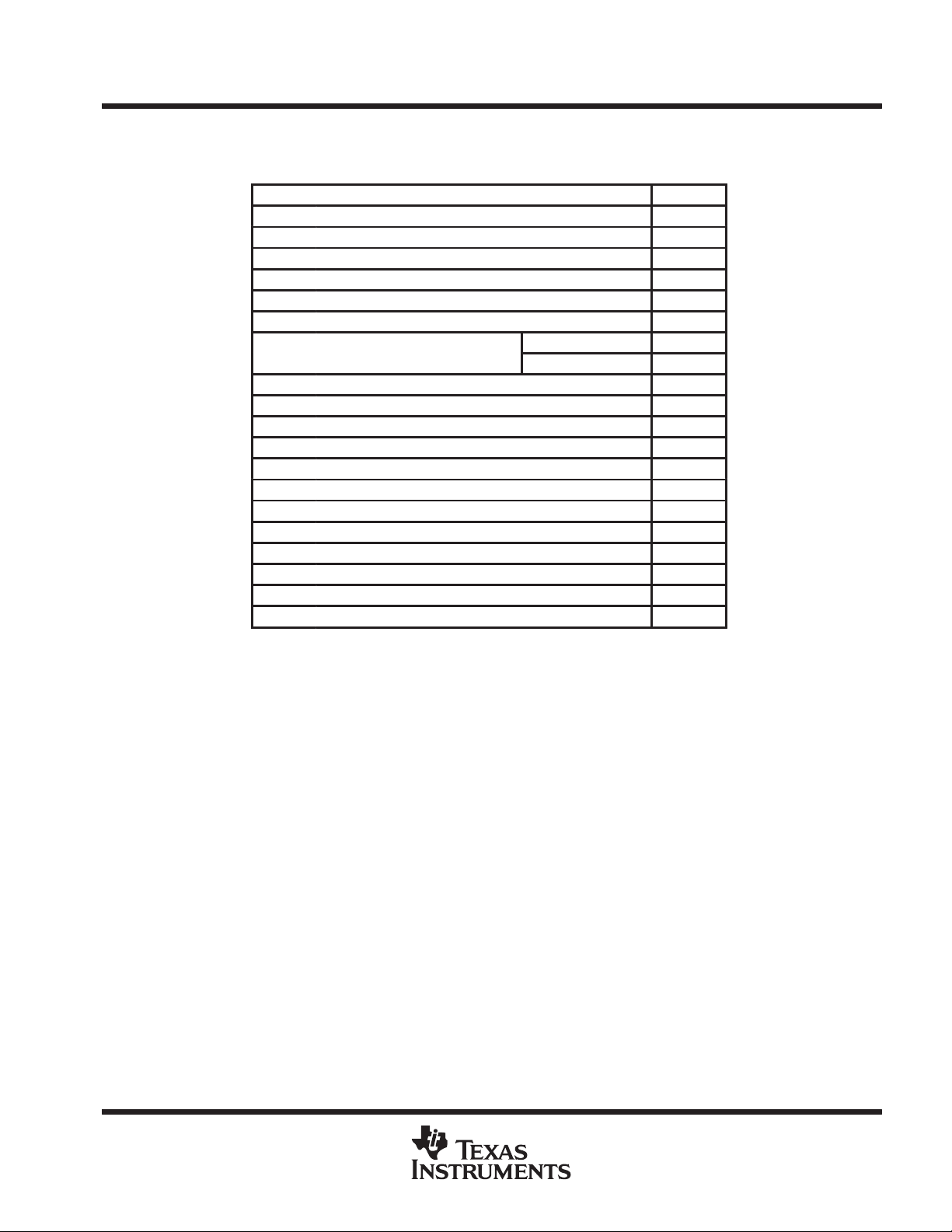
operating characteristics, VCC± = ±15 V, V
PARAMETER TEST CONDITIONS MIN TYP MAX
SR Slew rate 0.2 0.4 V/µs
p
V
N(PP)
I
n
Peak-to-peak equivalent input noise voltage f = 0.1 Hz to 10 Hz 0.55 µV
Equivalent input noise current f = 10 Hz 0.07 pA/√Hz
= 0, TA = 25°C
IC
f = 10 Hz 24
f = 1 kHz 22
UNIT
n
z
6
POST OFFICE BOX 655303 • DALLAS, TEXAS 75265
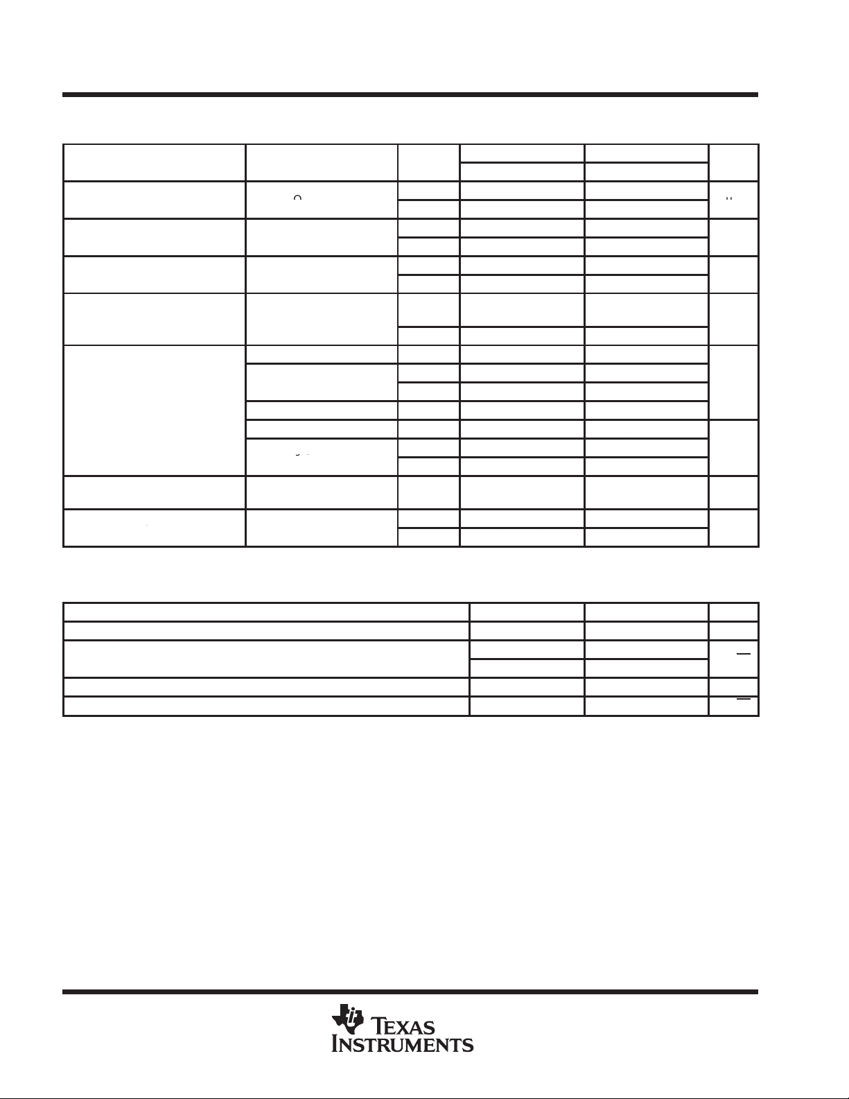
PARAMETER
TEST CONDITIONS
T
†
UNIT
VIOInput offset voltage
R
Ω
V
IIOInput offset current
nA
IIBInput bias current
nA
ICR
i
V
R
2 kΩ
V
voltage am lification
V
±10 V
R
kΩ
CMRR
V
V
dB
k
V
±18 V
dB
I
y
mA
LT1014, LT1014A, LT1014D
QUAD PRECISION OPERATIONAL AMPLIFIERS
SLOS039C – JULY 1989 – REVISED SEPTEMBER 1999
electrical characteristics at specified free-air temperature, V
noted)
p
a
V
A
r
id
r
ic
CC
†
Full range is –40°C to 105°C.
‡
All typical values are at TA = 25°C.
T emperature coeficient
V
IO
of input offset voltage
Long-term drift
of input offset voltage
p
p
Common-mode
p
nput voltage range
Maximum peak
OM
output voltage swing
Large-signal differential
VD
Common-mode
rejection ratio
Supply-voltage
rejection ratio
SVR
(∆VCC/∆VIO)
Channel separation VO = ±10 V, RL = 2 kΩ 25°C 120 137 120 137 dB
Differential
input resistance
Common-mode
input resistance
Supply current
per amplifier
p
A
= 50
S
=
L
VO = ±10 V, RL = 600 Ω 25°C 0.5 2 0.5 2
=
,
O
= –15 V to 13.5
IC
= ±2 V to
CC±
L
= 2
25°C 60 300 200 800
Full range 550 1000
Full range 0.4 2.5 0.7 5 µV/°C
25°C 0.5 0.5 µV/mo
25°C 0.15 1.5 0.15 1.5
Full range 2.8 2.8
25°C –12 –30 –12 –30
Full range –38 –38
25°C
Full range
25°C ±12.5 ±14 ±12.5 ±14
Full range ±12 ±12
25°C 1.2 8 1.2 8
Full range 0.7 0.7
25°C 97 117 97 117
Full range 94 94
25°C 100 117 100 117
Full range 97 97
25°C 70 300 70 300 MΩ
25°C 4 4 GΩ
25°C 0.35 0.55 0.35 0.55
Full range 0.6 0.6
MIN
–15
13.5
–15
to 13
= ±15 V , VIC = 0 (unless otherwise
CC±
LT1014I LT1014DI
‡
to
13.8
MAX MIN
–15
to
13.5
–15
to 13
TYP
–15.3
to
TYP
–15.3
13.8
‡
MAX
to
µ
V
V/µV
POST OFFICE BOX 655303 • DALLAS, TEXAS 75265
7
LT1014, LT1014A, LT1014D
PARAMETER
TEST CONDITIONS
T
†
UNIT
VIOInput offset voltage
R
Ω
V
IIOInput offset current
nA
IIBInput bias current
nA
ICR
in ut voltage range
,
mV
out ut voltage swing
g,
I
y
mA
VnEquivalent input noise voltage
V/√H
QUAD PRECISION OPERATIONAL AMPLIFIERS
SLOS039C – JULY 1989 – REVISED SEPTEMBER 1999
electrical characteristics at specified free-air temperature, V
(unless otherwise noted)
p
p
p
V
V
A
CC
†
Full range is –40°C to 105°C.
Common-mode
p
Maximum peak
OM
VD
p
Large-signal differential
voltage amplification
Supply current
per amplifier
A
= 50
S
Output low, No load 25°C 15 25 15 25
Output low,
RL = 600 Ω to GND
Output low, I
Output high, No load 25°C 4 4.4 4 4.4
Output high,
RL = 600 Ω to GND
VO = 5 mV to 4 V,
RL = 500 Ω
= 1 mA 25°C 220 350 220 350
sink
25°C 90 450 250 950
Full range 570 1200
25°C 0.2 2 0.2 2
Full range 6 6
25°C –15 –50 –15 –50
Full range –90 –90
25°C
Full range 0 to 3 0 to 3
25°C 5 10 5 10
Full range 13 13
25°C 3.4 4 3.4 4
Full range 3.2 3.2
25°C 1 1 V/µV
25°C 0.3 0.5 0.3 0.5
Full range 0.55 0.55
MIN
to 3.5
= 5 V , V
CC+
LT1014I LT1014DI
MAX MIN
TYP
0
–0.3
to 3.8
= 0, VO = 1.4 V , V
CC–
0
to 3.5
to 3.8
TYP
–0.3
MAX
IC
= 0
µ
V
V
operating characteristics, VCC+ = ±15 V, V
PARAMETER TEST CONDITIONS MIN TYP MAX
SR Slew rate 0.2 0.4 V/µs
p
V
N(PP)
I
n
Peak-to-peak equivalent input noise voltage f = 0.1 Hz to 10 Hz 0.55 µV
Equivalent input noise current f = 10 Hz 0.07 pA/√Hz
= 0, TA = 25°C
IC
f = 10 Hz 24
f = 1 kHz 22
UNIT
n
z
8
POST OFFICE BOX 655303 • DALLAS, TEXAS 75265
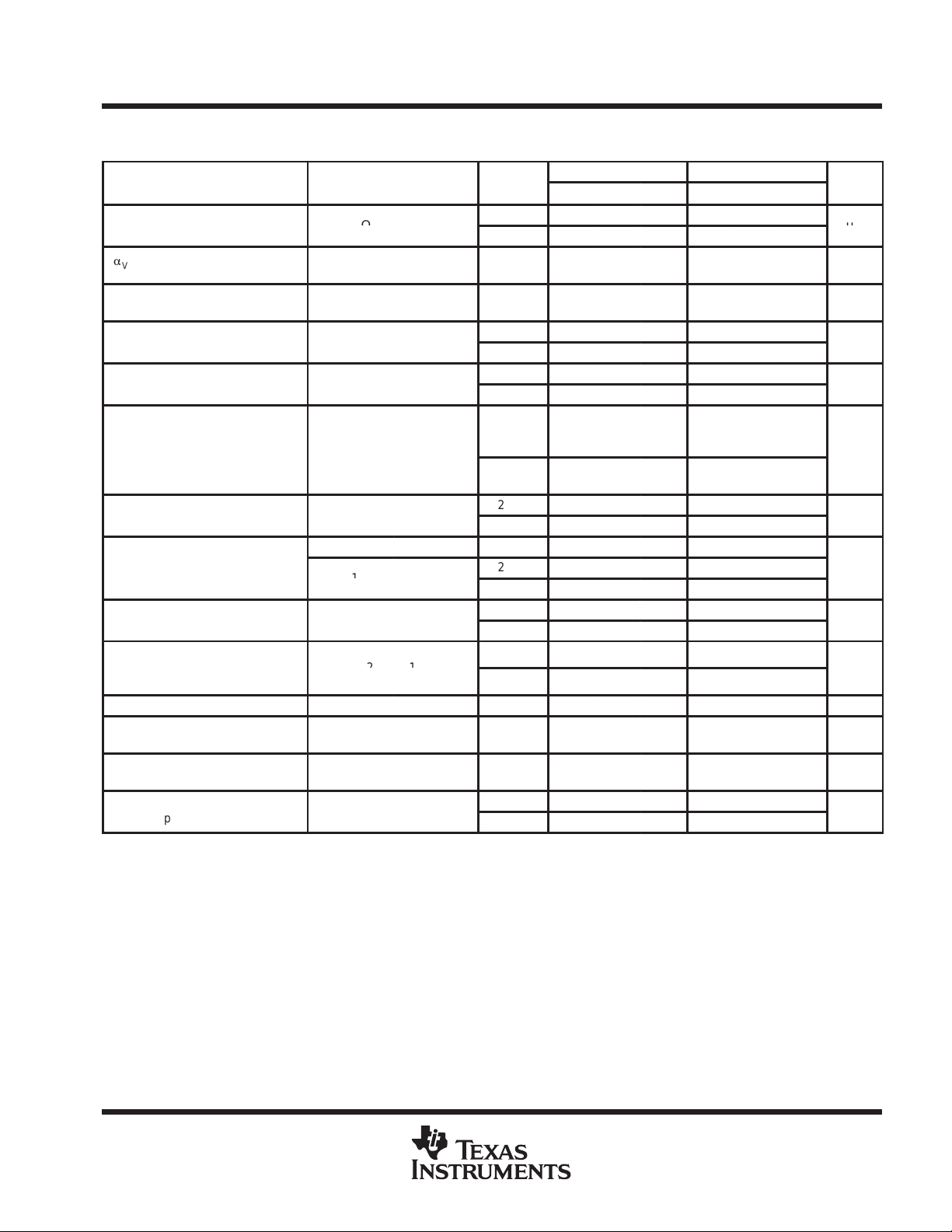
PARAMETER
T
†
UNIT
V
R
50 Ω
V
I
nA
I
nA
g
ICR
g
V
R
kΩ
V
differential
O
,
CMRR
dB
k
CC±
dB
I
y
mA
LT1014, LT1014A, LT1014D
QUAD PRECISION OPERATIONAL AMPLIFIERS
SLOS039C – JULY 1989 – REVISED SEPTEMBER 1999
electrical characteristics at specified free-air temperature, V
noted)
LT1014M LT1014AM LT1014DM
MIN TYP‡MAX MIN TYP‡MAX MIN TYP‡MAX
–15
–15.3
to
13.5
–14.9
to 13
to
13.8
CONDITIONS
Input offset
IO
voltage
Temperature
V
IO
OM
VD
SVR
coefficient of
input offset
voltage
Long-term drift
of input offset
voltage
Input offset
current
Input bias
current
Common-mode
input volta
range
Maximum peak
output voltage
swing
Large-signal
differential
voltage
amplification
Common-mode
rejection ratio
Supply-voltage
rejection ratio
(∆VCC/∆VIO)
Channel
separation
Differential input
resistance
Common-mode
input resistance
Supply current
per amplifier
e
p
VO = ±10 V,
RL = 600 Ω
V
RL = 2 kΩ
VIC = –15 V to
13.5 V
VIC = –14.9 V
to 13 V
V
±18 V
VO = ±10 V,
RL = 2 kΩ
a
IO
IB
V
A
r
id
r
ic
CC
†
Full range is –55°C to 125°C.
‡
All typical values are at TA = 25°C.
TEST
=
S
= 2
L
= ±10 V,
= ±2 V to
A
25°C 60 300 60 180 200 800
Full range 550 350 1000
Full range 0.5 2.5 0.5 2 0.5 2.5 µV/°C
25°C 0.5 0.5 0.5 µV/mo
25°C 0.15 1.5 0.15 0.8 0.15 1.5
Full range 5 2.8 5
25°C –12 –30 –12 –20 –12 –30
Full range –45 –30 –45
25°C
Full range
25°C ±12.5 ±14 ±13 ±14 ±12.5 ±14
Full range ±11.5 ±12 ±11.5
25°C 0.5 2 0.8 2.2 0.5 2
25°C 1.2 8 1.5 8 1.2 8
Full range 0.25 0.4 0.25
25°C 97 117 100 117 97 117
Full range 94 96 94
25°C 100 117 103 117 100 117
Full range 97 100 97
25°C 120 137 123 137 120 137 dB
25°C 70 300 100 300 70 300 MΩ
25°C 4 4 4 GΩ
25°C 0.35 0.55 0.35 0.50 0.35 0.55
Full range 0.7 0.6 0.7
= ±15 V , VIC = 0 (unless otherwise
CC±
–15
13.5
–14.9
to 13
–15.3
to
to
13.8
–15
13.5
–14.9
to 13
–15.3
to
to
13.8
µ
V
V/µV
POST OFFICE BOX 655303 • DALLAS, TEXAS 75265
9

LT1014, LT1014A, LT1014D
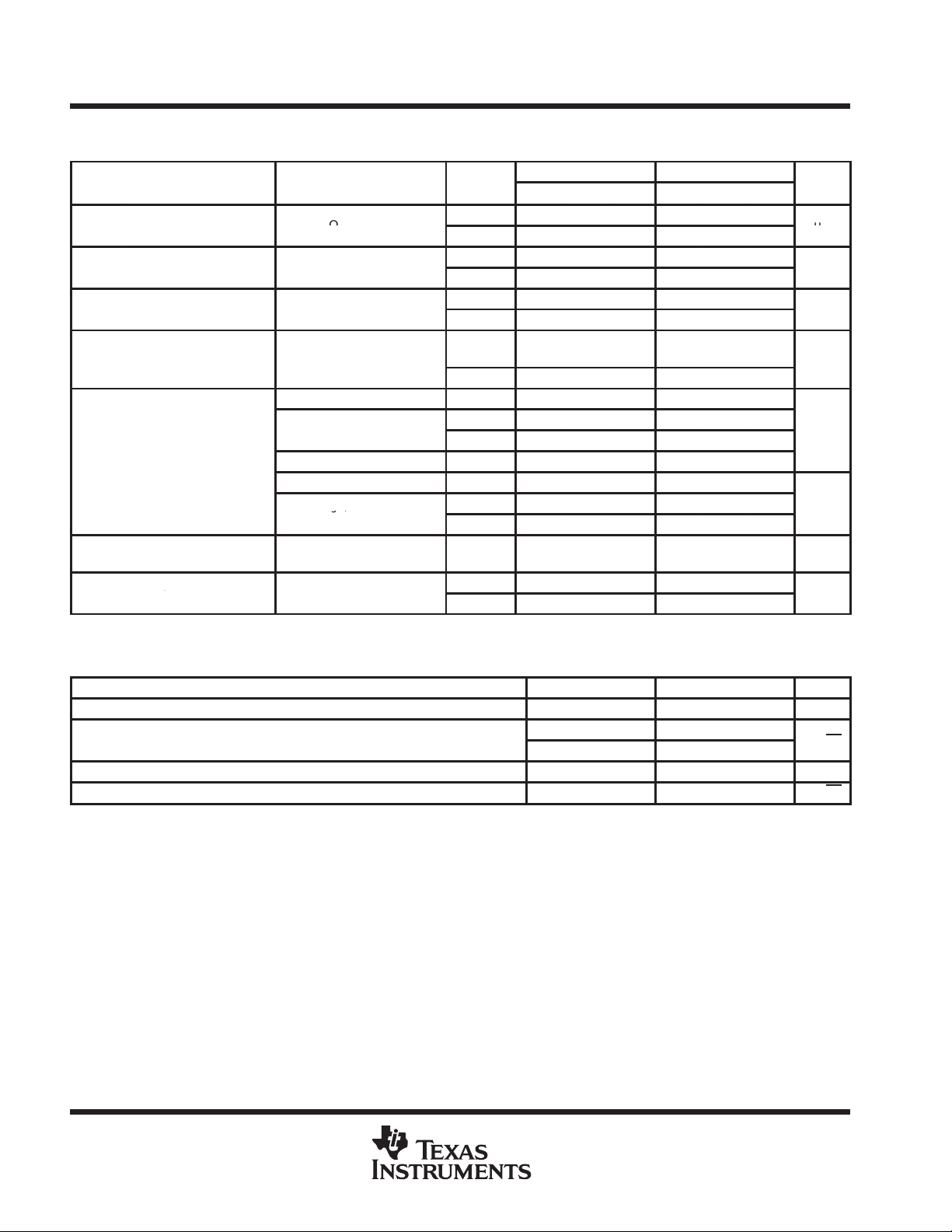
PARAMETER
T
†
UNIT
R
50Ω
V
IO
µV
I
nA
I
V
t
V
R
600Ω t
mV
voltage swing
I
y
mA
VnEquivalent input noise voltage
V/√H
QUAD PRECISION OPERATIONAL AMPLIFIERS
SLOS039C – JULY 1989 – REVISED SEPTEMBER 1999
electrical characteristics at specified free-air temperature, V
(unless otherwise noted)
LT1014M LT1014AM LT1014DM
MIN TYP MAX MIN TYP MAX MIN TYP MAX
0
to 3.5
–0.3
to 3.8
0.1
to 3
Input
offset voltage
Input
IO
offset current
Input
IB
bias current
Commonmode inpu
ICR
V
OM
A
VD
CC
†
Full range is –55°C to 125°C.
p
voltage range
Maximum
peak output
Large-signal
differential
voltage
amplification
Supply current
per amplifier
TEST
CONDITIONS
=
S
RS = 50Ω,
VIC = 0.1 V
Output low,
No load
Output low,
=
L
GND
Output low,
I
sink
Output high,
No load
Output high, 25°C 3.4 4 3.4 4 3.4 4
RL = 600Ω to
GND
VO = 5 mV to 4 V,
RL = 500Ω
o
= 1 mA
A
25°C 90 450 90 280 250 950
Full range 400 1500 400 960 800 2000
125°C 200 750 200 480 560 1200
25°C 0.2 2 0.2 1.3 0.2 2
Full range 10 7 10
25°C –15 –50 –15 –35 –15 –50
Full range –120 –90 –120
25°C
Full range
25°C 15 25 15 25 15 25
25°C 5 10 5 10 5 10
Full range 18 15 18
25°C 220 350 220 350 220 350
25°C 4 4.4 4 4.4 4 4.4
Full range 3.1 3.2 3.1
25°C 1 1 1 V/µV
25°C 0.3 0.5 0.3 0.45 0.3 0.5
Full range 0.65 0.55 0.65
CC+
to 3.5
0.1
to 3
= 5 V , V
0
–0.3
to 3.8
CC–
= 0, V
0
to 3.5
0.1
to 3
= 1.4 V , VIC = 0
O
–0.3
to 3.8
V
operating characteristics, V
SR Slew rate 0.2 0.4 V/µs
V
N(PP)
I
n
10
Peak-to-peak equivalent input noise voltage f = 0.1 Hz to 10 Hz 0.55 µV
Equivalent input noise current f = 10 Hz 0.07 pA/√Hz
= ±15 V, VIC = 0, TA = 25°C
CC±
PARAMETER TEST CONDITIONS MIN TYP MAX
p
POST OFFICE BOX 655303 • DALLAS, TEXAS 75265
f = 10 Hz 24
f = 1 kHz 22
UNIT
n
z
AVDDifferential voltage amplification
LT1014, LT1014A, LT1014D
QUAD PRECISION OPERATIONAL AMPLIFIERS
SLOS039C – JULY 1989 – REVISED SEPTEMBER 1999
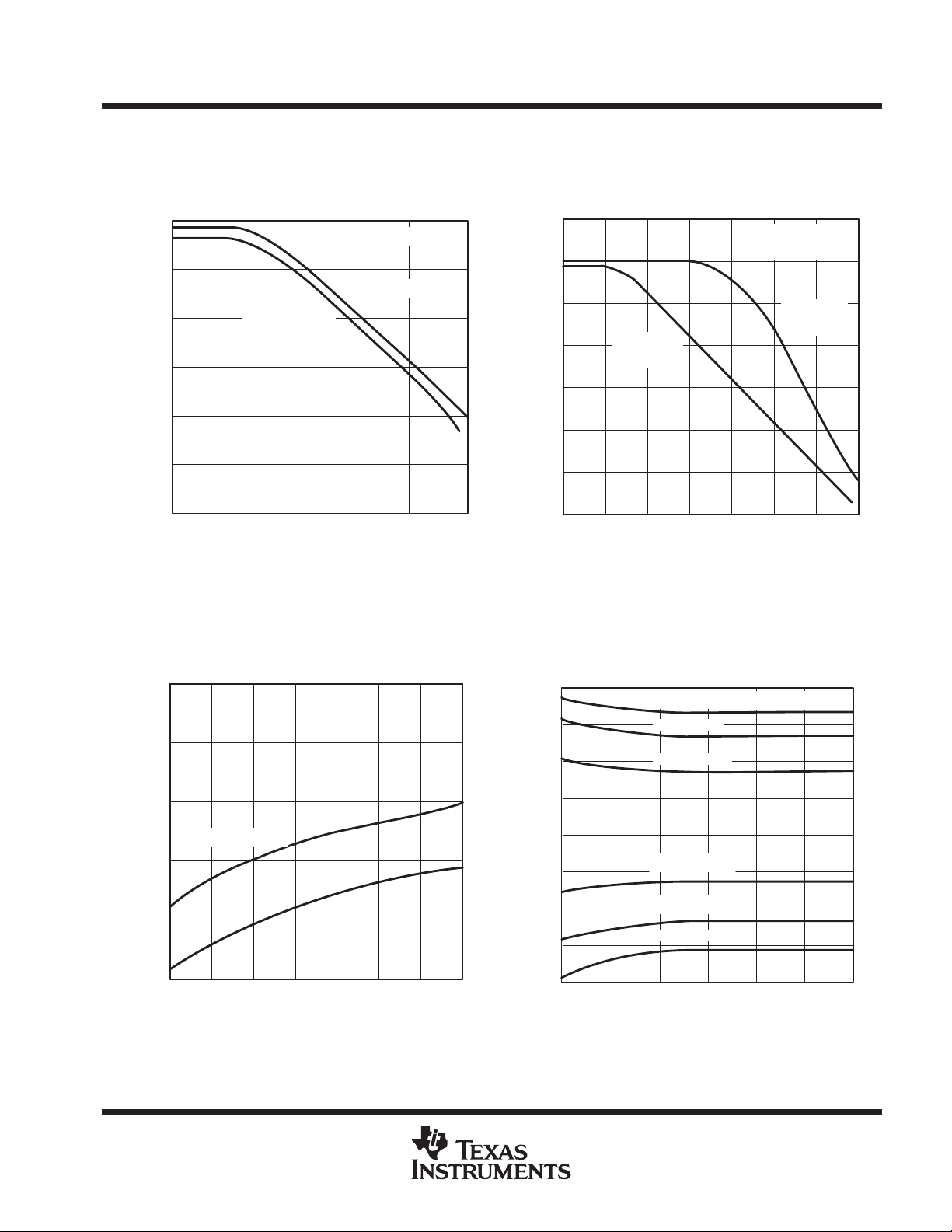
TYPICAL CHARACTERISTICS
Table of Graphs
FIGURE
V
IO
V
IO
∆V
I
IO
I
IB
V
IC
CMRR Common-mode rejection ratio vs Frequency 13
k
SVR
I
CC
I
OS
V
n
I
n
V
N(PP)
Input offset voltage vs Balanced source resistance 1
Input offset voltage vs Free-air temperature 2
Warm-Up Change in input offset voltage vs Elapsed time 3
IO
Input offset current vs Free-air temperature 4
Input bias current vs Free-air temperature 5
Common-mode input voltage vs Input bias current 6
p
Channel separation vs Frequency 11
Output saturation voltage vs Free-air temperature 12
Supply-voltage rejection ratio vs Frequency 14
Supply current vs Free-air temperature 15
Short-circuit output current vs Elapsed time 16
Equivalent input noise voltage vs Frequency 17
Equivalent input noise current vs Frequency 17
Peak-to-peak input noise voltage vs Time 18
Pulse response (small signal) vs Time 19, 21
Pulse response (large signal) vs Time 20, 22, 23
Phase shift vs Frequency 9
vs Load resistance 7, 8
vs Frequency 9, 10
POST OFFICE BOX 655303 • DALLAS, TEXAS 75265
11

LT1014, LT1014A, LT1014D
QUAD PRECISION OPERATIONAL AMPLIFIERS
SLOS039C – JULY 1989 – REVISED SEPTEMBER 1999
10
TA = 25°C
1
V
V
0.1
– Input Offset Voltage – mV
IO
V
V
0.01
1 k
TYPICAL CHARACTERISTICS
LT1014
INPUT OFFSET VOLTAGE
vs
BALANCED SOURCE RESISTANCE
= 5 V
CC±
= 0
CC–
R
S
= ±15 V
CC±
3 k 10 k 30 k 100 k 300 k 1 M 3 M 10 M
Rs – Source Resistance – Ω
–
+
R
S
†
INPUT OFFSET VOLTAGE
OF REPRESENTATIVE UNITS
vs
250
V
200
Vµ– Input Offset Voltage –V
150
100
50
0
–50
–100
IO
–150
–200
–250
–50 –25 0 25 50 75 100 125
FREE-AIR TEMPERATURE
= ±15 V
CC±
TA – Free-Air Temperature – °C
Figure 1
WARM-UP CHANGE IN INPUT OFFSET VOLTAGE
vs
ELAPSED TIME
5
V
= ±15 V
Vµ
– Change in Input Offset Votlage –
IO
∆V
CC±
TA = 25°C
4
3
2
N Package
1
0
0123
t – Time After Power-On – min
J Package
45
Figure 3
Figure 2
INPUT OFFSET CURRENT
vs
FREE-AIR TEMPERATURE
1
VIC = 0
0.8
0.6
V
= ±2.5 V
CC–
CC±
= 0
0.4
V
= 5 V, V
– Input Offset Current – nAI
IO
0.2
0
–50 –25 0 25 50 75 100 125
CC+
V
= ±15 V
CC±
TA – Free-Air Temperature – °C
Figure 4
†
Data at high and low temperatures are applicable only within the rated operating free-air temperature ranges of the various devices.
12
POST OFFICE BOX 655303 • DALLAS, TEXAS 75265

LT1014, LT1014A, LT1014D
QUAD PRECISION OPERATIONAL AMPLIFIERS
SLOS039C – JULY 1989 – REVISED SEPTEMBER 1999
TYPICAL CHARACTERISTICS
INPUT BIAS CURRENT
vs
–30
–25
–20
–15
–10
– Input Bias Current – nAI
IB
–5
0
–50 –25 0 25 50 75 100 125
FREE-AIR TEMPERATURE
VIC = 0
V
= 5 V, V
CC
+
V
= ±15 V
CC±
TA – Free-Air Temperature – °C
CC–
= 0
V
CC±
= ±2.5 V
†
COMMON-MODE INPUT VOLTAGE
vs
INPUT BIAS CURRENT
15
TA = 25°C
10
5
V
= ±15 V
CC±
(Left Scale)
0
–5
– Common-Mode Input Voltage – VV
–10
IC
–15
0 –5 –10 –15 –20 –25 –30
IIB – Input Bias Current – nA
V
= 5 V
CC+
V
= 0
CC–
(Right Scale)
5
4
3
2
1
0
–1
– Common-Mode Input Voltage – VV
IC
Figure 5
DIFFERENTIAL VOLTAGE AMPLIFICATION
vs
10
Vµ– Differential Voltage Amplivication – V/A
V
CC±
VO = ±10 V
4
TA = –55°C
1
0.4
VD
0.1
100 400 1 k 4 k 10 k
LOAD RESISTANCE
= ±15 V
TA = 25°C
TA = 125°C
RL – Load Resistance – Ω
Figure 6
DIFFERENTIAL VOLTAGE AMPLIFICATION
vs
10
Vµ– Differential Voltage Amplivication – V/A
V
CC+
VO = 20 mV to 3.5 V
4
1
0.4
VD
0.1
100 400 1 k 4 k 10 k
LOAD RESISTANCE
= 5 V, V
= 0
CC–
RL – Load Resistance – Ω
TA = –55°C
TA = 25°C
TA = 125°C
Figure 7
†
Data at high and low temperatures are applicable only within the rated operating free-air temperature ranges of the various devices.
POST OFFICE BOX 655303 • DALLAS, TEXAS 75265
Figure 8
13

LT1014, LT1014A, LT1014D
φ
QUAD PRECISION OPERATIONAL AMPLIFIERS
SLOS039C – JULY 1989 – REVISED SEPTEMBER 1999
TYPICAL CHARACTERISTICS
DIFFERENTIAL VOLTAGE AMPLIFICATION
AND PHASE SHIFT
vs
FREQUENCY
VIC = 0
20
A
VD
10
V
CC+
0
V
– Differential Voltage Amplivication – dBA
–10
VD
0.01 0.3 1 3 10
V
CC±
= 5 V
= 0
CC–
VCC± = ±15 V
f – Frequency – MHz
= ±15 V
Figure 9
CL = 100 pF
TA = 25°C
V
= 5 V
CC+
V
= 0
CC–
80°
100°100°
120°
140°
160°
180°
200°
220°
240°
140
120
100
80
60
– Phase Shift
40
20
– Differential Voltage Amplivication – dBA
0
VD
–20
†
DIFFERENTIAL VOLTAGE AMPLIFICATION
vs
FREQUENCY
CL = 100 pF
TA = 25°C
VCC + = 5 V
VCC – = 0
0.01 0.1 1 k 100 k 10 M1 10 100 10 k 1 M
f – Frequency – Hz
V
CC±
= ±15 V
Figure 10
CHANNEL SEPARATION
vs
160
140
Limited by
Thermal
120
Interaction
100
Channel Separation – dB
80
60
10 100 1 k 10 k
f – Frequency – Hz
Figure 11
†
Data at high and low temperatures are applicable only within the rated operating free-air temperature ranges of the various devices.
V
V
RL = 2 kΩ
TA = 25°C
RL = 1 kΩ
Limited by
Pin-to-Pin
Capacitance
= ±15 V
CC±
= 20 V to 5 kHz
I(PP)
RL = 100 Ω
100 k 1 M
FREQUENCY
10
0.1
Output Saturation Voltage – V
0.01
OUTPUT SATURATION VOLTAGE
vs
FREE-AIR TEMPERATURE
V
= 5 V to 30 V
CC+
V
= 0
CC–
I
= 10 mA
sink
1
I
= 5 mA
sink
I
= 1 mA
sink
I
= 100 µA
sink
I
= 10 µA
sink
I
= 0
sink
–50 –25 0 25 50 75 100 125
TA – Free-Air Temperature – °C
Figure 12
14
POST OFFICE BOX 655303 • DALLAS, TEXAS 75265
LT1014, LT1014A, LT1014D
QUAD PRECISION OPERATIONAL AMPLIFIERS
SLOS039C – JULY 1989 – REVISED SEPTEMBER 1999
TYPICAL CHARACTERISTICS
COMMON-MODE REJECTION RATIO
vs
FREQUENCY
120
100
V
= ±15 V
CC±
V
80
60
40
20
CMRR – Common-Mode Rejection Ratio – dB
0
10 100 1 k 10 k
= 5 V
CC+
V
= 0
CC–
f – Frequency – Hz
TA = 25°C
100 k 1 M
†
SUPPLY-VOLTAGE REJECTION RATIO
140
120
100
80
60
40
– Supply-Voltage Rejection Ratio – dBK
20
SVR
0
0.1 1 10 100 1 k
Negative
Supply
f – Frequency – Hz
vs
FREQUENCY
V
= ± 15 V
CC±
TA = 25°C
Positive
Supply
10 k 100 k 1 M
AµI
– Supply Current Per Amplifier –
CC
460
420
380
340
300
260
Figure 13
SUPPLY CURRENT
vs
FREE-AIR TEMPERATURE
V
= ±15 V
CC±
V
= 5 V
CC+
V
= 0
CC–
–25–50
0 25 50 75 100 125
TA – Free-Air Temperature – °C
Figure 14
SHORT-CIRCUIT OUTPUT CURRENT
40
30
20
10
0
–10
–20
– Short-Circuit Output Current – mAI
OS
–30
–40
01
ELAPSED TIME
TA = –55°C
TA = 25°C
TA = 125°C
TA = 125°C
TA = 25°C
TA = –55°C
t – Time – min
vs
V
= ±15 V
CC±
23
Figure 15
†
Data at high and low temperatures are applicable only within the rated operating free-air temperature ranges of the various devices.
POST OFFICE BOX 655303 • DALLAS, TEXAS 75265
Figure 16
15
LT1014, LT1014A, LT1014D
QUAD PRECISION OPERATIONAL AMPLIFIERS
SLOS039C – JULY 1989 – REVISED SEPTEMBER 1999
TYPICAL CHARACTERISTICS
EQUIVALENT INPUT NOISE VOLTAGE
AND EQUIVALENT INPUT NOISE CURRENT
vs
1000
V
= ±2 V to ±18 V
CC±
fA/ Hz
– Equivalent Input Noise Voltage –V
TA = 25°C
300
I
n
100
V
n
30
n
1/f Corner = 2 Hz
10
110
FREQUENCY
100
f – Frequency – Hz
Figure 17
1 k
1000
300
100
30
10
fA/ Hz
– Equivalent Input Noise Current – I
PEAK-TO-PEAK INPUT NOISE VOLTAGE
OVER A 10-SECOND PERIOD
vs
TIME
2000
V
= ±2 V to ±18 V
CC±
f = 0.1 Hz to 10 Hz
TA = 25°C
1600
1200
800
– Noise Voltage – nVV
N(PP)
400
n
0
0246
t – Time – s
810
Figure 18
VOLTAGE-FOLLOWER SMALL-SIGNAL
PULSE RESPONSE
vs
TIME
80
V
= ±15 V
CC±
AV = 1
60
TA = 25°C
40
20
0
–20
– Output Voltage – mVV
O
–40
–60
–80
46810
20
t – Time – µs
12 14
– Output Voltage – VV
O
Figure 19
VOLTAGE-FOLLOWER LARGE-SIGNAL
PULSE RESPONSE
vs
TIME
6
V
= 5 V
CC+
V
= 0
CC–
5
VI = 0 to 4 V
RL = 0
4
AV = 1
TA = 25°C
3
2
1
0
–1
–2
0102030
t – Time – µs
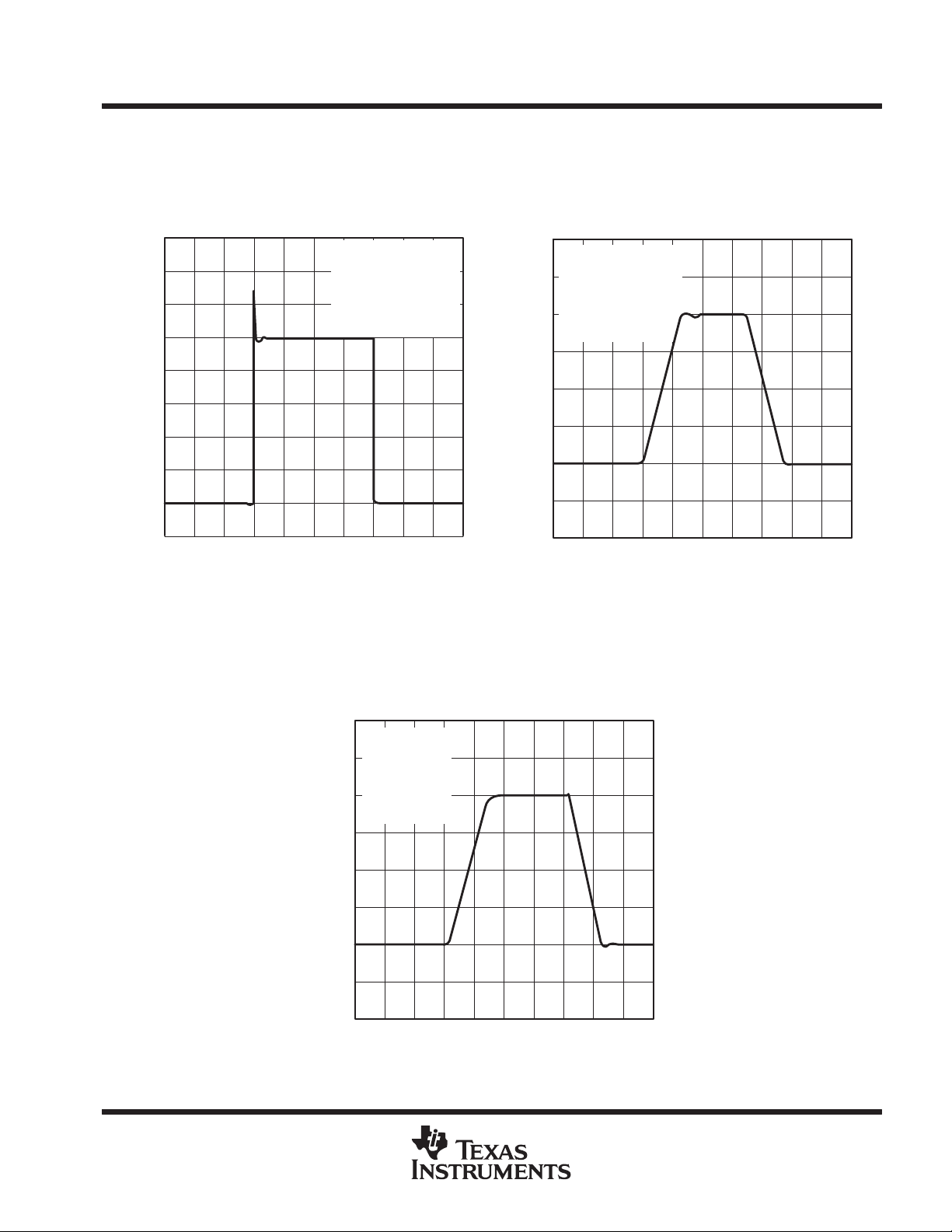
Figure 20
40 50 60 70
16
POST OFFICE BOX 655303 • DALLAS, TEXAS 75265
LT1014, LT1014A, LT1014D
QUAD PRECISION OPERATIONAL AMPLIFIERS
SLOS039C – JULY 1989 – REVISED SEPTEMBER 1999
TYPICAL CHARACTERISTICS
VOLTAGE-FOLLOWER SMALL-SIGNAL
PULSE RESPONSE
vs
TIME
160
140
120
100
80
60
– Output Voltage – mVV
40
O
20
0
–20
0204060
t – Time – µs
V
= 5 V
CC+
V
= 0
CC–
VI = 0 to 100 mV
RL = 600 Ω to GND
AV = 1
TA = 25°C
80 100 120 140
– Output Voltage – mVV
Figure 21
VOLTAGE-FOLLOWER LARGE-SIGNAL
PULSE RESPONSE
vs
TIME
6
V
= 5 V
CC+
V
= 0
CC–
5
VI = 0 to 4 V
RL = 4.7 kΩ to 5 V
4
AV = 1
TA = 25°C
3
2
1
O
0
–1
–2
0102030
t – Time – µs
Figure 22
40 50 60 70
VOLTAGE-FOLLOWER LARGE-SIGNAL
PULSE RESPONSE
vs
TIME
6
V
= 5 V
CC+
V
= 0
CC–
5
VI = 0 to 4 V
RL = 0
4
AV = 1
TA = 25°C
3
2
1
– Output Voltage – VV
O
0
–1
–2
0102030
t – Time – µs
40 50 60 70
Figure 23
POST OFFICE BOX 655303 • DALLAS, TEXAS 75265
17
LT1014, LT1014A, LT1014D
QUAD PRECISION OPERATIONAL AMPLIFIERS
SLOS039C – JULY 1989 – REVISED SEPTEMBER 1999
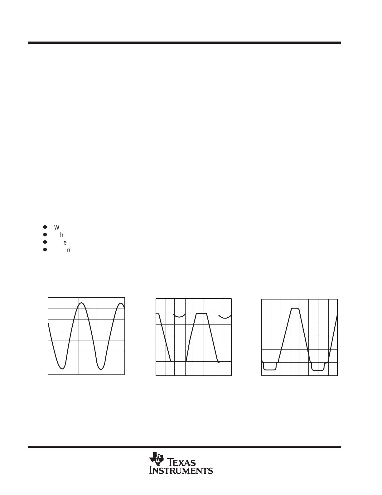
APPLICATION INFORMATION
single-supply operation
The LT1014 is fully specified for single-supply operation (V
= 0). The common-mode input voltage range
CC–
includes ground, and the output swings within a few millivolts of ground.
Furthermore, the LT1014 has specific circuitry that addresses the difficulties of single-supply operation, both
at the input and at the output. At the input, the driving signal can fall below 0 V, either inadvertently or on a
transient basis. If the input is more than a few hundred millivolts below ground, the L T1014 is designed to deal
with the following two problems that can occur:
1. On many other operational amplifiers, when the input is more than a diode drop below ground, unlimited
current flows from the substrate (V
terminal) to the input, which can destroy the unit. On the LT1014,
CC–
the 400-Ω resistors in series with the input (see schematic) protect the device even when the input is 5 V
below ground.
2. When the input is more than 400 mV below ground (at TA = 25°C), the input stage of similar type operational
amplifiers saturates, and phase reversal occurs at the output. This can cause lockup in servo systems.
Because of unique phase-reversal protection circuitry (Q21, Q22, Q27, and Q28), the LT1014 outputs do
not reverse, even when the inputs are at –1.5 V (see Figure 24).
However, this phase-reversal protection circuitry does not function when the other operational amplifier on the
LT1014 is driven hard into negative saturation at the output. Phase-reversal protection does not work on an
amplifier:
D
When 4’s output is in negative saturation (the outputs of 2 and 3 have no effect)
D
When 3’s output is in negative saturation (the outputs of 1 and 4 have no effect)
D
When 2’s output is in negative saturation (the outputs of 1 and 4 have no effect)
D
When 1’s output is in negative saturation (the outputs of 2 and 3 have no effect)
At the output, other single-supply designs either cannot swing to within 600 mV of ground or cannot sink more
than a few microproamperes while swinging to ground. The all-npn output stage of the L T1014 maintains its low
output resistance and high gain characteristics until the output is saturated. In dual-supply operations, the output
stage is free of crossover distortion.
18
– Input Voltage – VV
I(PP)
–1
–2
5
4
3
2
1
0
(a) V
= –1.5 V to 4.5 V (b) Output Phase Reversal
I(PP)
5
4
3
2
1
– Output Voltage – VV
O
0
–1
Exhibited by LM358
5
4
3
2
1
– Output Voltage – VV
O
0
–1
(c) No Phase Reversal
Exhibited by LT1014
Figure 24. Voltage-Follower Response
With Input Exceeding the Negative Common-Mode Input Voltage Range
POST OFFICE BOX 655303 • DALLAS, TEXAS 75265

LT1014, LT1014A, LT1014D
QUAD PRECISION OPERATIONAL AMPLIFIERS
SLOS039C – JULY 1989 – REVISED SEPTEMBER 1999
APPLICATION INFORMATION
comparator applications
The single-supply operation of the L T1014 can be used as a precision comparator with TTL-compatible output.
In systems using both operational amplifiers and comparators, the LT1014 can perform multiple duties (see
Figures 25 and 26).
5
4
10 mV 5 mV 2 mV
3
2
– Output Voltage – VV
1
O
0
Differential
Input Voltage
100 mV
0 50 100 150 200 250 300 350 400 450
t – Time – µs
Overdrive
V
CC+
V
CC–
TA = 25°C
= 5 V
= 0
Figure 25. Low-to-High-Level Output Response
for Various Input Overdrives
5
4
3
2
10 mV
– Output Voltage – VV
1
O
0
Differential
Input Voltage
Overdrive
100 mV
0 50 100 150 200 250 300 350 400 450
t – Time – µs
V
= 5 V
CC+
V
= 0
CC–
TA = 25°C
2 mV5 mV
Figure 26. High-to-Low-Level Output Response
for Various Input Overdrives
low-supply operation
The minimum supply voltage for proper operation of the L T1014 is 3.4 V (three Ni-Cad batteries). Typical supply
current at this voltage is 290 µA; therefore, power dissipation is only 1 mW per amplifier.
offset voltage and noise testing
Figure 30 shows the test circuit for measuring input offset voltage and its temperature coefficient. This circuit
with supply voltages increased to ±20 V is also used as the burn-in configuration.
The peak-to-peak equivalent input noise voltage of the LT1014 is measured using the test circuit shown in
Figure 27. The frequency response of the noise tester indicates that the 0.1-Hz corner is defined by only one
zero. The test time to measure 0.1-Hz to 10-Hz noise should not exceed 10 seconds, as this time limit acts as
an additional zero to eliminate noise contribution from the frequency band below 0.1 Hz.
An input noise-voltage test is recommended when measuring the noise of a large number of units. A 10-Hz input
noise-voltage measurement correlates well with a 0.1-Hz peak-to-peak noise reading because both results are
determined by the white noise and the location of the 1/f corner frequency.
Noise current is measured by the circuit and formula shown in Figure 28. The noise of the source resistors is
subtracted.
POST OFFICE BOX 655303 • DALLAS, TEXAS 75265
19

LT1014, LT1014A, LT1014D
QUAD PRECISION OPERATIONAL AMPLIFIERS
SLOS039C – JULY 1989 – REVISED SEPTEMBER 1999
APPLICATION INFORMATION
0.1 µF
100 kΩ
10 Ω
NOTE A: All capacitor values are for nonpolarized capacitors only.
+
LT1014
–
AVD = 50,000
2 kΩ
4.7 µF
24.3 kΩ
Figure 27. 0.1-Hz to 10-Hz Peak-to-Peak Noise Test Circuit
10 kΩ
†
Metal-film resistor
†
10 MΩ
100 Ω
10 MΩ†10 MΩ
10 MΩ
†
†
+
LT1014
–
+
LT1001
–
100 kΩ
0.1 µF
V
n
4.3 kΩ
2.2 µF
In+
ƪ
V
no
22 µF
*(820 nV
2
40 MW
Oscilloscope
Rin = 1 MΩ
110 kΩ
1ń2
2
ƫ
)
100
Figure 28. Noise-Current Test Circuit and Formula
100 Ω
(see Note A)
50 Ω
(see Note A)
NOTE A: Resistors must have low thermoelectric potential.
Figure 29. Test Circuit for VIO and αV
50 Ω
(see Note A)
15 V
+
LT1014
–
–15 V
VO = 1000 V
IO
IO
20
POST OFFICE BOX 655303 • DALLAS, TEXAS 75265
LT1014, LT1014A, LT1014D
QUAD PRECISION OPERATIONAL AMPLIFIERS
SLOS039C – JULY 1989 – REVISED SEPTEMBER 1999
APPLICATION INFORMATION
5 V
Q3
2N2905
68 Ω
Q4
2N2222
2 kΩ
100 pF
0.33 µF
5 V
5 V
1/4
LT1014
4.3 kΩ
SN74HC04 (6)
0.002 µF
10 kΩ
10 kΩ 10 kΩ
±
+
4 kΩ
10 kΩ
LT1004
1.2 V
820 Ω
10 µF
820 Ω
100 kΩ
†
†
1 kΩ
4-mA
Trim
+
LT1014
1/4
Q1
2N2905
T1
Q2
2N2905
±
+
IN
0 to 4 V
‡
10 µF
10 Ω
10 kΩ
20-mA
Trim
80 Ω
1N4002 (4)
+
†
†
†
†
100 Ω
4-mA to 20-mA OUT
To Load
2.2 kΩ Max
†
1% film resistor. Match 10-kΩ resistors 0.05%.
‡
T1 = PICO-31080
Figure 30. 5-V Powered, 4-mA to 20-mA Current-Loop Transmitter With 12-Bit Accuracy
POST OFFICE BOX 655303 • DALLAS, TEXAS 75265
21

LT1014, LT1014A, LT1014D
QUAD PRECISION OPERATIONAL AMPLIFIERS
SLOS039C – JULY 1989 – REVISED SEPTEMBER 1999
APPLICATION INFORMATION
1N4002 (4)
+
4-mA to 20-mA OUT
Fully Floating
To
Inverter
Driver
†
1% film resistor
5 V
5 V
1/4
LT1014
4.3 kΩ
LT1004
1.2 V
0.1 Ω
1/4
LT1014
†
†
+
–
†
4 kΩ
2 kΩ
4-mA
Trim
100 kΩ
†
IN
0 to 4 V
68 kΩ
301 Ω
1 kΩ
20-mA
Trim
–
+
10 kΩ
T1
10 µF
Figure 31. Fully Floating Modification to 4-mA to 20-mA Current-Loop Transmitter With 8-Bit Accuracy
1/2 LTC1043
6
IN+
18 15
IN–
5
2
1 µF
3
1 µF
5
6
5 V
+
1/4
LT1014
–
8
7
4
OUT A
R2
1/2 LTC1043
7
IN+
11
12
13 14
IN–
NOTE A: VIO = 150 µV, AVD = (R1/R2) + 1, CMRR = 120 dB, V
8
1 µF
0.01 µF
Figure 32. 5-V Single-Supply Dual Instrumentation Amplifier
1 µF
= 0 to 5 V
ICR
3
2
+
1/4
LT1014
–
R1
1
OUT B
R2
R1
22
POST OFFICE BOX 655303 • DALLAS, TEXAS 75265

LT1014, LT1014A, LT1014D
QUAD PRECISION OPERATIONAL AMPLIFIERS
SLOS039C – JULY 1989 – REVISED SEPTEMBER 1999
APPLICATION INFORMATION
10
IN–
IN+
20 kΩ
1 µF
20 kΩ
5 V
‡
‡
‡
‡
200 kΩ
2
–
LT1014
3
+
RG (2 kΩ Typ)
200 kΩ
6
–
LT1014
5
+
+
†
1
7
9
10 kΩ
10 kΩ
10 kΩ
10 kΩ
LT1014
–
†
†
13
12
8
–
LT1014
+
10 kΩ
To Input
Cable Shields
10 kΩ
5 V
4
11
†
14
†
OUT
5 V
††
1% film resistor. Match 10-kΩ resistors 0.05%.
‡
For high source impedances, use 2N2222 as diodes (with collector connected to base).
NOTE A: AVD = (400,000/RG) + 1
Figure 33. 5-V Powered Precision Instrumentation Amplifier
POST OFFICE BOX 655303 • DALLAS, TEXAS 75265
23

PACKAGE OPTION ADDENDUM
www.ti.com
6-Jun-2005
PACKAGING INFORMATION
Orderable Device Status
(1)
Package
Type
Package
Drawing
Pins Package
Qty
Eco Plan
5962-89677012A ACTIVE LCCC FK 20 1 TBD POST-PLATE Level-NC-NC-NC
5962-8967701CA ACTIVE CDIP J 14 1 TBD A42 SNPB Level-NC-NC-NC
5962-89677022A ACTIVE LCCC FK 20 1 TBD POST-PLATE Level-NC-NC-NC
5962-8967702CA ACTIVE CDIP J 14 1 TBD A42 SNPB Level-NC-NC-NC
LT1014AMFKB ACTIVE LCCC FK 20 1 TBD POST-PLATE Level-NC-NC-NC
LT1014AMJ ACTIVE CDIP J 14 1 TBD A42 SNPB Level-NC-NC-NC
LT1014AMJB ACTIVE CDIP J 14 1 TBD A42 SNPB Level-NC-NC-NC
LT1014CN ACTIVE PDIP N 14 25 Pb-Free
LT1014CNE4 ACTIVE PDIP N 14 25 Pb-Free
LT1014DDW ACTIVE SOIC DW 16 40 Green (RoHS &
no Sb/Br)
LT1014DDWE4 ACTIVE SOIC DW 16 40 Green (RoHS &
no Sb/Br)
LT1014DDWR ACTIVE SOIC DW 16 2000 Green (RoHS &
no Sb/Br)
LT1014DDWRE4 ACTIVE SOIC DW 16 2000 Green (RoHS &
no Sb/Br)
LT1014DIDW ACTIVE SOIC DW 16 40 Green (RoHS &
no Sb/Br)
LT1014DIDWR OBSOLETE SOIC DW 16 TBD Call TI Call TI
LT1014DIN ACTIVE PDIP N 14 25 Pb-Free
LT1014DINE4 ACTIVE PDIP N 14 25 Pb-Free
LT1014DMDW ACTIVE SOIC DW 16 40 TBD CU NIPDAU Level-1-220C-UNLIM
LT1014DN ACTIVE PDIP N 14 25 Pb-Free
LT1014DNE4 ACTIVE PDIP N 14 25 Pb-Free
LT1014IN OBSOLETE PDIP N 14 TBD Call TI Call TI
LT1014MFKB ACTIVE LCCC FK 20 1 TBD POST-PLATE Level-NC-NC-NC
LT1014MJ ACTIVE CDIP J 14 1 TBD A42 SNPB Level-NC-NC-NC
LT1014MJB ACTIVE CDIP J 14 1 TBD A42 SNPB Level-NC-NC-NC
(1)
The marketing status values are defined as follows:
ACTIVE: Product device recommended for new designs.
LIFEBUY: TI has announced that the device will be discontinued, and a lifetime-buy period is in effect.
NRND: Not recommended for new designs. Device is in production to support existing customers, but TI does not recommend using this part in
a new design.
PREVIEW: Device has been announced but is not in production. Samples may or may not be available.
OBSOLETE: TI has discontinued the production of the device.
(RoHS)
(RoHS)
(RoHS)
(RoHS)
(RoHS)
(RoHS)
(2)
Lead/Ball Finish MSL Peak Temp
CU NIPDAU Level-NC-NC-NC
CU NIPDAU Level-NC-NC-NC
CU NIPDAU Level-1-260C-UNLIM
CU NIPDAU Level-1-260C-UNLIM
CU NIPDAU Level-1-260C-UNLIM
CU NIPDAU Level-1-260C-UNLIM
CU NIPDAU Level-1-260C-UNLIM
CU NIPDAU Level-NC-NC-NC
CU NIPDAU Level-NC-NC-NC
CU NIPDAU Level-NC-NC-NC
CU NIPDAU Level-NC-NC-NC
(3)
(2)
Eco Plan - The planned eco-friendly classification: Pb-Free (RoHS) or Green (RoHS & no Sb/Br) - please check
http://www.ti.com/productcontent for the latest availability information and additional product content details.
TBD: The Pb-Free/Green conversion plan has not been defined.
Pb-Free (RoHS): TI's terms "Lead-Free" or "Pb-Free" mean semiconductor products that are compatible with the current RoHS requirements
for all 6 substances, including the requirement that lead not exceed 0.1% by weight in homogeneous materials. Where designed to be soldered
Addendum-Page 1

PACKAGE OPTION ADDENDUM
www.ti.com
at high temperatures, TI Pb-Free products are suitable for use in specified lead-free processes.
Green (RoHS & no Sb/Br): TI defines "Green" to mean Pb-Free (RoHS compatible), and free of Bromine (Br) and Antimony (Sb) based flame
retardants (Br or Sb do not exceed 0.1% by weight in homogeneous material)
(3)
MSL, Peak Temp. -- The Moisture Sensitivity Level rating according to the JEDEC industry standard classifications, and peak solder
temperature.
Important Information and Disclaimer:The information provided on this page represents TI's knowledge and belief as of the date that it is
provided. TI bases its knowledge and belief on information provided by third parties, and makes no representation or warranty as to the
accuracy of such information. Efforts are underway to better integrate information from third parties. TI has taken and continues to take
reasonable steps to provide representative and accurate information but may not have conducted destructive testing or chemical analysis on
incoming materials and chemicals. TI and TI suppliers consider certain information to be proprietary, and thus CAS numbers and other limited
information may not be available for release.
In no event shall TI's liability arising out of such information exceed the total purchase price of the TI part(s) at issue in this document sold by TI
to Customer on an annual basis.
6-Jun-2005
Addendum-Page 2

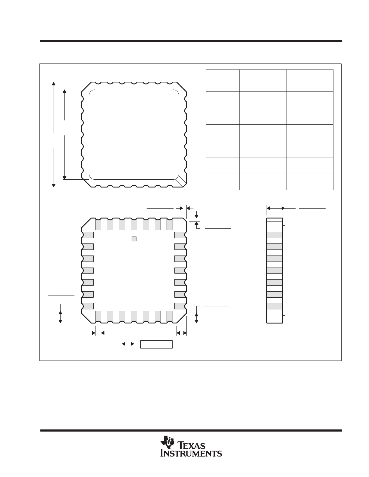
MECHANICAL DATA
MLCC006B – OCTOBER 1996
FK (S-CQCC-N**) LEADLESS CERAMIC CHIP CARRIER
28 TERMINAL SHOWN
A SQ
B SQ
19
20
22
23
24
25
21
12826 27
12
1314151618 17
0.020 (0,51)
0.010 (0,25)
MIN
0.342
(8,69)
0.442
0.640
0.739
0.938
1.141
A
0.358
(9,09)
0.458
(11,63)
0.660
(16,76)
0.761
(19,32)(18,78)
0.962
(24,43)
1.165
(29,59)
NO. OF
TERMINALS
**
11
10
9
8
7
6
5
432
20
28
44
52
68
84
0.020 (0,51)
0.010 (0,25)
(11,23)
(16,26)
(23,83)
(28,99)
MINMAX
0.307
(7,80)
0.406
(10,31)
0.495
(12,58)
0.495
(12,58)
0.850
(21,6)
1.047
(26,6)
0.080 (2,03)
0.064 (1,63)
B
MAX
0.358
(9,09)
0.458
(11,63)
0.560
(14,22)
0.560
(14,22)
0.858
(21,8)
1.063
(27,0)
0.055 (1,40)
0.045 (1,14)
0.028 (0,71)
0.022 (0,54)
0.050 (1,27)
NOTES: A. All linear dimensions are in inches (millimeters).
B. This drawing is subject to change without notice.
C. This package can be hermetically sealed with a metal lid.
D. The terminals are gold plated.
E. Falls within JEDEC MS-004
POST OFFICE BOX 655303 • DALLAS, TEXAS 75265
0.045 (1,14)
0.035 (0,89)
0.045 (1,14)
0.035 (0,89)
4040140/D 10/96


IMPORTANT NOTICE
Texas Instruments Incorporated and its subsidiaries (TI) reserve the right to make corrections, modifications,
enhancements, improvements, and other changes to its products and services at any time and to discontinue
any product or service without notice. Customers should obtain the latest relevant information before placing
orders and should verify that such information is current and complete. All products are sold subject to TI’s terms
and conditions of sale supplied at the time of order acknowledgment.
TI warrants performance of its hardware products to the specifications applicable at the time of sale in
accordance with TI’s standard warranty. Testing and other quality control techniques are used to the extent TI
deems necessary to support this warranty . Except where mandated by government requirements, testing of all
parameters of each product is not necessarily performed.
TI assumes no liability for applications assistance or customer product design. Customers are responsible for
their products and applications using TI components. To minimize the risks associated with customer products
and applications, customers should provide adequate design and operating safeguards.
TI does not warrant or represent that any license, either express or implied, is granted under any TI patent right,
copyright, mask work right, or other TI intellectual property right relating to any combination, machine, or process
in which TI products or services are used. Information published by TI regarding third-party products or services
does not constitute a license from TI to use such products or services or a warranty or endorsement thereof.
Use of such information may require a license from a third party under the patents or other intellectual property
of the third party, or a license from TI under the patents or other intellectual property of TI.
Reproduction of information in TI data books or data sheets is permissible only if reproduction is without
alteration and is accompanied by all associated warranties, conditions, limitations, and notices. Reproduction
of this information with alteration is an unfair and deceptive business practice. TI is not responsible or liable for
such altered documentation.
Resale of TI products or services with statements different from or beyond the parameters stated by TI for that
product or service voids all express and any implied warranties for the associated TI product or service and
is an unfair and deceptive business practice. TI is not responsible or liable for any such statements.
Following are URLs where you can obtain information on other Texas Instruments products and application
solutions:
Products Applications
Amplifiers amplifier.ti.com Audio www.ti.com/audio
Data Converters dataconverter.ti.com Automotive www.ti.com/automotive
DSP dsp.ti.com Broadband www.ti.com/broadband
Interface interface.ti.com Digital Control www.ti.com/digitalcontrol
Logic logic.ti.com Military www.ti.com/military
Power Mgmt power.ti.com Optical Networking www.ti.com/opticalnetwork
Microcontrollers microcontroller.ti.com Security www.ti.com/security
Telephony www.ti.com/telephony
Video & Imaging www.ti.com/video
Wireless www.ti.com/wireless
Mailing Address: Texas Instruments
Post Office Box 655303 Dallas, Texas 75265
Copyright 2005, Texas Instruments Incorporated
 Loading...