

L293D
QUADRUPLE HALF-H DRIVER
SLRS008A – SEPTEMBER 1986 – REVISED MAY 1990
• 600-mA Output Current Capability Per
Driver
• Pulsed Current 1.2-A Per Driver
• Output Clamp Diodes for Inductive
Transient Suppression
• Wide Supply Voltage Range
4.5 V to 36 V
• Separate Input-Logic Supply
• Thermal Shutdown
• Internal ESD Protection
• High-Noise-Immunity Inputs
• Functional Replacement for SGS L293D
description
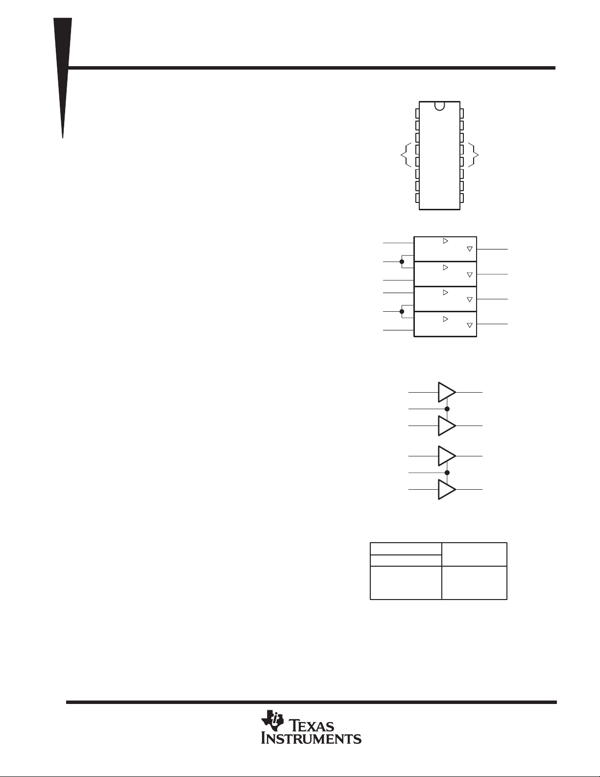
The L293D is a quadruple high-current half-H
driver designed to provide bidirectional drive
currents of up to 600-mA at voltages from 4.5 V to
36 V . It is designed to drive inductive loads such as
relays, solenoids, dc and bipolar stepping motors,
as well as other high-current/high-voltage loads in
positive-supply applications.
All inputs are TTL-compatible. Each output is a
complete totem-pole drive circuit with a Darlington
transistor sink and a pseudo-Darlington source.
Drivers are enabled in pairs with drivers 1 and 2
enabled by 1,2EN and drivers 3 and 4 enabled by
3,4EN. When an enable input is high, the
associated drivers are enabled, and their outputs
are active and in phase with their inputs. External
high-speed output clamp diodes should be used
for inductive transient suppression. When the
enable input is low, those drivers are disabled, and
their outputs are off and in a high-impedance
state. With the proper data inputs, each pair of
drivers form a full-H (or bridge) reversible drive
suitable for solenoid or motor applications.
A V
for the logic inputs to minimize device power
dissipation.
The L293D is designed for operation from 0°C
to 70°C.
terminal, separate from V
CC1
CC2
, is provided
NE PACKAGE
(TOP VIEW)
1,2EN
HEAT SINK AND
GROUND
V
1A
2A
3A
4A
†
2
1
7
10
9
15
logic symbol
1,2EN
3,4EN
†
This symbol is in accordance with ANSI/IEEE Std 91-1984
and IEC Publication 617-12.
1A
1Y
2Y
2A
CC2
1
2
3
4
5
6
7
8
EN
EN
EN
EN
16
15
14
13
12
11
10
9
V
CC1
4A
4Y
HEAT SINK AND
GROUND
3Y
3A
3,4EN
3
6
11
14
logic diagram
2
1A
1,2EN
3,4EN
H = high-level, L = low level,
X = irrelevant, Z = high-impedance (off)
‡
In the thermal shutdown mode, the
output is in the high-impedance state
regardless of the input levels.
1
7
2A
10
3A
9
15
4A
FUNCTION TABLE
(each driver)
‡
INPUTS
AEN
H
L
X
H
H
L
3
6
11
14
OUTPUT
Y
H
L
Z
1Y
2Y
3Y
4Y
1Y
2Y
3Y
4Y
PRODUCTION DATA information is current as of publication date.
Products conform to specifications per the terms of Texas Instruments
standard warranty. Production processing does not necessarily include
testing of all parameters.
POST OFFICE BOX 655303 • DALLAS, TEXAS 75265
Copyright 1990, Texas Instruments Incorporated
3–1
L293D
High-level input voltage, V
V
QUADRUPLE HALF-H DRIVER
SLRS008A – SEPTEMBER 1986 – REVISED MAY 1990
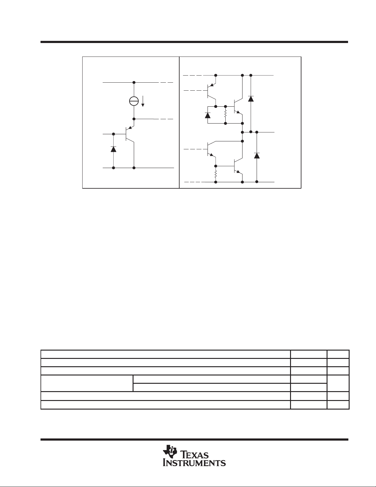
schematics of inputs and outputs
EQUIVALENT OF EACH INPUT
V
CC1
Current
Source
Input
GND
TYPICAL OF ALL OUTPUTS
V
CC2
Output
GND
absolute maximum ratings over operating free-air temperature range (unless otherwise noted)
Logic supply voltage range, V
Output supply voltage range, V
Input voltage range, VI 7 V. . . . . . . . . . . . . . . . . . . . . . . . . . . . . . . . . . . . . . . . . . . . . . . . . . . . . . . . . . . . . . . . . . . . . . .
Output voltage range, V
–3 V to V
O
Peak output current (nonrepetitive, t ≤ 100 µs) ±1.2 A. . . . . . . . . . . . . . . . . . . . . . . . . . . . . . . . . . . . . . . . . . . . . . .
Continuous output current, IO ±600 mA. . . . . . . . . . . . . . . . . . . . . . . . . . . . . . . . . . . . . . . . . . . . . . . . . . . . . . . . . . .
Continuous total dissipation at (or below) 25°C free-air temperature (see Notes 2 and 3) 2075 mW. . . . . . .
Continuous total dissipation at 80°C case temperature (see Note 3) 5000 mW. . . . . . . . . . . . . . . . . . . . . . . . .
Operating case or virtual junction temperature range, T
Storage temperature range, T
Lead temperature 1,6 mm (1/16 inch) from case for 10 seconds 260°C. . . . . . . . . . . . . . . . . . . . . . . . . . . . . . .
NOTES: 1. All voltage values are with respect to the network ground terminal.
2. For operation above 25°C free-air temperature, derate linearly at the rate of 16.6 mW/°C.
3. For operation above 25°C case temperature, derate linearly at the rate of 71.4 mW/°C. Due to variations in individual device electrical
characteristics and thermal resistance, the built-in thermal overload protection may be activated at power levels slightly above or
below the rated dissipation.
(see Note 1) 36 V. . . . . . . . . . . . . . . . . . . . . . . . . . . . . . . . . . . . . . . . . . . . . . .
CC1
36 V. . . . . . . . . . . . . . . . . . . . . . . . . . . . . . . . . . . . . . . . . . . . . . . . . . . . . . . . . .
CC2
–40°C to 150°C. . . . . . . . . . . . . . . . . . . . . . . . . . . . .
–65°C to 150°C. . . . . . . . . . . . . . . . . . . . . . . . . . . . . . . . . . . . . . . . . . . . . . . . . .
stg
J
CC2
+ 3 V. . . . . . . . . . . . . . . . . . . . . . . . . . . . . . . . . . . . . . . . . . . . . . . . . . . . .
recommended operating conditions
Logic supply voltage, V
Output supply voltage, V
Low-level input voltage, V
Operating free-air temperature, T
†
The algebraic convention, in which the least positive (most negative) value is designated minimum, is used in this data sheet for logic voltage
levels.
3–2
MIN MAX UNIT
CC1
CC2
V
≤ 7 V 2.3 V
p
IH
IL
A
CC1
V
≥ 7 V 2.3 7
CC1
POST OFFICE BOX 655303 • DALLAS, TEXAS 75265
4.5 7 V
V
CC1
–0.3
36 V
CC1
†
1.5 V
0 70 °C

L293D
IIHHigh-level input current
V
7 V
A
IILLow-level input current
V
0
A
C
30 pF
See Figure 1
QUADRUPLE HALF-H DRIVER
SLRS008A – SEPTEMBER 1986 – REVISED MAY 1990
electrical characteristics, V
PARAMETER TEST CONDITIONS MIN TYP MAX UNIT
V
V
V
V
I
CC1
I
CC2
High-level output voltage IOH = –0.6 A V
OH
Low-level output voltage IOL = 0.6 A 1.2 1.8 V
OL
High-level output clamp voltage IOK = –0.6 A V
OKH
Low-level output clamp voltage IOK = –0.6 A 1.3 V
OKL
p
p
Logic supply current IO = 0
Output supply current IO = 0
switching characteristics, V
PARAMETER TEST CONDITIONS MIN TYP MAX UNIT
t
Propagation delay time, low-to-high-level output from A input 800 ns
PLH
t
Propagation delay time, high-to-low-level output from A input
PHL
t
Transition time, low-to-high-level output
TLH
t
Transition time, high-to-low-level output 300 ns
THL
CC1
A
EN
A
EN
CC1
= 5 V, V
=
I
=
I
= 5 V, V
= 24 V, TA = 25°C
CC2
–1.8 V
CC2
All outputs at high level 13 22
All outputs at low level 35 60
All outputs at high impedance 8 24
All outputs at high level 14 24
All outputs at low level 2 6
All outputs at high impedance 2 4
= 24 V, TA = 25°C
CC2
p
=
L
,
CC2
CC2
–1.4 V
+1.3 V
0.2 100
0.2 ±10
–3 –10
–2 –100
400 ns
300 ns
µ
µ
mA
mA
PARAMETER MEASUREMENT INFORMATION
t
f
90%
5 V 24 VInput
V
Pulse
Generator
(see Note A)
3 V
NOTES: A. The pulse generator has the following characteristics: tr ≤ 10 ns, tf ≤ 10 ns, tw = 10 µs, PRR = 5 kHz, ZO = 50 Ω.
B. CL includes probe and jig capacitance.
CC1VCC2
A
EN
GND
TEST CIRCUIT
Y
Output
CL = 30 pF
(see Note B)
Input
Output
1.5 V
10%
90% 90%
VOLTAGE WAVEFORMS
10%
t
w
t
PHL
50%
10% 10%
t
THL
Figure 1. Test Circuit and Voltage Waveforms
t
1.5 V
50%
r
90%
t
PLH
t
TLH
3 V
0
V
V
OH
OL
POST OFFICE BOX 655303 • DALLAS, TEXAS 75265
3–3

L293D
QUADRUPLE HALF-H DRIVER
SLRS008A – SEPTEMBER 1986 – REVISED MAY 1990
10 kΩ
1,2EN
1
APPLICATION INFORMATION
V
CC1
16
24 V5 V
V
CC2
3
Control A
Control B
1A
2A
3,4EN
3A
10
1Y
2
7
9
3
Motor
2Y
6
3Y
11
3–4
4A
15
Thermal
Shutdown
4, 5, 12, 13
GND
Figure 2. T wo-Phase Motor Driver
POST OFFICE BOX 655303 • DALLAS, TEXAS 75265
4Y
14

IMPORTANT NOTICE
T exas Instruments and its subsidiaries (TI) reserve the right to make changes to their products or to discontinue
any product or service without notice, and advise customers to obtain the latest version of relevant information
to verify, before placing orders, that information being relied on is current and complete. All products are sold
subject to the terms and conditions of sale supplied at the time of order acknowledgement, including those
pertaining to warranty, patent infringement, and limitation of liability.
TI warrants performance of its semiconductor products to the specifications applicable at the time of sale in
accordance with TI’s standard warranty. T esting and other quality control techniques are utilized to the extent
TI deems necessary to support this warranty . Specific testing of all parameters of each device is not necessarily
performed, except those mandated by government requirements.
CERTAIN APPLICATIONS USING SEMICONDUCTOR PRODUCTS MAY INVOLVE POTENTIAL RISKS OF
DEATH, PERSONAL INJURY, OR SEVERE PROPERTY OR ENVIRONMENTAL DAMAGE (“CRITICAL
APPLICATIONS”). TI SEMICONDUCTOR PRODUCTS ARE NOT DESIGNED, AUTHORIZED, OR
WARRANTED TO BE SUITABLE FOR USE IN LIFE-SUPPORT DEVICES OR SYSTEMS OR OTHER
CRITICAL APPLICA TIONS. INCLUSION OF TI PRODUCTS IN SUCH APPLICATIONS IS UNDERST OOD TO
BE FULLY AT THE CUSTOMER’S RISK.
In order to minimize risks associated with the customer’s applications, adequate design and operating
safeguards must be provided by the customer to minimize inherent or procedural hazards.
TI assumes no liability for applications assistance or customer product design. TI does not warrant or represent
that any license, either express or implied, is granted under any patent right, copyright, mask work right, or other
intellectual property right of TI covering or relating to any combination, machine, or process in which such
semiconductor products or services might be or are used. TI’s publication of information regarding any third
party’s products or services does not constitute TI’s approval, warranty or endorsement thereof.
Copyright 1998, Texas Instruments Incorporated
 Loading...