

www.ti.com
IWR6843, IWR6443
SWRS219D – OCTOBER 2018 – REVISED SEPTEMBER 2020
SWRS219D – OCTOBER 2018 – REVISED SEPTEMBER 2020
IWR6843, IWR6443
IWR6843, IWR6443 Single-Chip 60- to 64-GHz mmWave Sensor
1 Features
• FMCW transceiver
– Integrated PLL, transmitter, receiver, Baseband,
and A2D
– 60- to 64-GHz coverage with 4-GHz continuous
bandwidth
– Four receive channels
– Three transmit channels
– Supports 6-bit phase shifter for TX Beam
forming
– Ultra-accurate chirp engine based on fractional-
N PLL
– TX power: 12 dBm
– RX noise figure:
• 12 dB
– Phase noise at 1 MHz:
• –93 dBc/Hz
• Built-in calibration and self-test
– ARM® Cortex®-R4F-based radio control system
– Built-in firmware (ROM)
– Self-calibrating system across frequency and
temperature
– Embedded self-monitoring with no host
processor involvement on Functional SafetyCompliant targeted devices
• C674x DSP for advanced signal processing
(IWR6843 only)
• Hardware accelerator for FFT, filtering, and CFAR
processing
• Memory compression
• ARM-R4F microcontroller for object detection, and
interface control
– Supports autonomous mode (loading user
application from QSPI flash memory)
• Internal memory with ECC
– IWR6843: 1.75 MB, divided into MSS program
RAM (512 KB), MSS data RAM (192 KB), DSP
L1 RAM (64KB) and L2 RAM (256 KB), and L3
radar data cube RAM (768 KB)
– IWR6443: 1.4 MB, divided into MSS program
RAM (512 KB), MSS data RAM (192 KB), and
L3 radar data cube RAM (768 KB)
– Technical reference manual includes allowed
size modifications
• Other interfaces available to user application
– Up to 6 ADC channels (low sample rate
monitoring)
– Up to 2 SPI ports
– Up to 2 UARTs
– 1 CAN-FD interface
– I2C
– GPIOs
– 2 lane LVDS interface for raw ADC data and
debug instrumentation
• Functional Safety-Compliant targeted
– Developed for functional safety applications
– Documentation will be available to aid IEC
61508 functional safety system design
– Hardware integrity up to SIL-2 targeted
– Safety-related certification
• IEC 61508 certification by TUV Sud planned
• Non-Functional safety variants
• Power management
– Built-in LDO network for enhanced PSRR
– I/Os support dual voltage 3.3 V/1.8 V
• Clock source
– 40.0 MHz crystal with internal oscillator
– Supports external oscillator at 40 MHz
– Supports externally driven clock (square/sine)
at 40 MHz
• Easy hardware design
– 0.65-mm pitch, 161-pin 10.4 mm × 10.4 mm flip
chip BGA package for easy assembly and lowcost PCB design
– Small solution size
• Operating conditions:
– Junction temperature range of –40°C to 105°C
An IMPORTANT NOTICE at the end of this data sheet addresses availability, warranty, changes, use in safety-critical applications,
Copyright © 2020 Texas Instruments Incorporated
intellectual property matters and other important disclaimers. PRODUCTION DATA.
Product Folder Links: IWR6843 IWR6443
Submit Document Feedback
1
IWR6843, IWR6443
SWRS219D – OCTOBER 2018 – REVISED SEPTEMBER 2020
www.ti.com
2 Applications
• Industrial sensor for measuring range, velocity, and
angle
• Building automation
• Displacement sensing
• Gesture recognition
• Traffic monitoring
• Proximity and position sensing
• Security and surveillance
• Factory automation safety guards
• People counting
• Motion detection
• Occupancy detection
• Robotics
3 Description
The IWR device is an integrated single chip mmWave sensor based on FMCW radar technology capable of
operation in the 60-GHz to 64-GHz band. It is built with TI’s low power 45-nm RFCMOS process and enables
unprecedented levels of integration in an extremely small form factor. This device is an ideal solution for low
power, self-monitored, ultra-accurate radar systems in the industrial space. Multiple variants are currently
available including Functional Safety-Compliant targeted devices and non-functional safety devices.
PART NUMBER PACKAGE
IWR6843AQGABL FCBGA (161) 10.4 mm × 10.4 mm Tray (Non-Functional Safety)
IWR6843AQGABLR FCBGA (161) 10.4 mm × 10.4 mm Tape and Reel (Non-Functional Safety)
IWR6843ABGABLR FCBGA (161) 10.4 mm × 10.4 mm Tape and Reel (Functional Safety-Compliant targeted, SIL2)
IWR6843ABGABL FCBGA (161) 10.4 mm × 10.4 mm Tray (Functional Safety-Compliant targeted, SIL2)
IWR6443AQGABL FCBGA (161) 10.4 mm × 10.4 mm Tray (Non-Functional Safety)
IWR6443AQGABLR FCBGA (161) 10.4 mm × 10.4 mm Tape and Reel (Non-Functional Safety)
(1)
Device Information
BODY SIZE TRAY / TAPE AND REEL
(1) For more information, see Section 13, Mechanical, Packaging, and Orderable Information.
2 Submit Document Feedback
Copyright © 2020 Texas Instruments Incorporated
Product Folder Links: IWR6843 IWR6443
IF ADC
Digital
Front-end
(Decimation
filter chain)
LNA
IF ADC
LNA
IF ADC
LNA
IF ADC
LNA
PA
PA
Synth
(20 GHz)
Ramp
Generator
x3
Osc.
GPADC
Temp
Cortex R4F
@ 200MHz
(User programmable)
Prog RAM
Data
RAM
Boot
ROM
QSPI
SPI
SPI / I2C
Debug
UARTs
CAN-FD
DMA
Test/
Debug
ADC
Buffer
LVDS
RF/Analog sub-system
Master sub-system
(Customer programmed)
Serial Flash interface
External MCU
interface
PMIC control
CAN-FD Communication
For debug
JTAG for debug/
development
High-speed ADC output
interface (for recording)
6
DSP sub-system
(Customer programmed)
Mailbox
Bus Matrix
HIL
High-speed input for
hardware-in-loop verification
C674x DSP
@600 MHz
(IWR6843 only)
L1P
(32kB)
L1D
(32kB)
L2
(256kB)
DMA CRC
Radar Data Memory
(L3)
HW
Accel
PA
Phase
Shift
Phase
Shift
Phase
Shift
www.ti.com
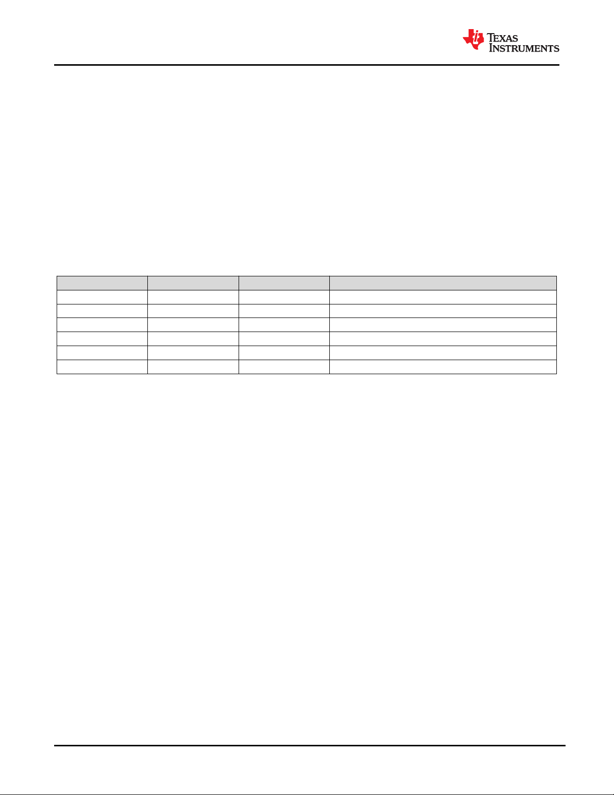
4 Functional Block Diagram
Figure 4-1 shows the functional block diagram of the device.
SWRS219D – OCTOBER 2018 – REVISED SEPTEMBER 2020
IWR6843, IWR6443
Figure 4-1. Functional Block Diagram
Submit Document Feedback
3
Copyright © 2020 Texas Instruments Incorporated
Product Folder Links: IWR6843 IWR6443

IWR6843, IWR6443
SWRS219D – OCTOBER 2018 – REVISED SEPTEMBER 2020
www.ti.com
Table of Contents
1 Features............................................................................1
2 Applications..................................................................... 2
3 Description.......................................................................2
4 Functional Block Diagram.............................................. 3
5 Revision History.............................................................. 5
6 Device Comparison......................................................... 6
6.1 Related Products........................................................ 7
7 Terminal Configuration and Functions..........................8
7.1 Pin Diagram................................................................ 8
7.2 Pin Attributes.............................................................13
7.3 Signal Descriptions................................................... 21
8 Specifications................................................................ 26
8.1 Absolute Maximum Ratings...................................... 26
8.2 ESD Ratings............................................................. 26
8.3 Power-On Hours (POH)............................................ 26
8.4 Recommended Operating Conditions.......................27
8.5 Power Supply Specifications.....................................28
8.6 Power Consumption Summary................................. 29
8.7 RF Specification........................................................30
8.8 CPU Specifications................................................... 30
8.9 Thermal Resistance Characteristics for FCBGA
Package [ABL0161].....................................................31
8.10 Timing and Switching Characteristics..................... 32
9 Detailed Description......................................................55
9.1 Overview................................................................... 55
9.2 Functional Block Diagram......................................... 55
9.3 Subsystems.............................................................. 56
9.4 Other Subsystems.................................................... 60
10 Monitoring and Diagnostics....................................... 62
10.1 Monitoring and Diagnostic Mechanisms................. 62
11 Applications, Implementation, and Layout............... 67
11.1 Application Information............................................67
11.2 Reference Schematic..............................................67
12 Device and Documentation Support..........................68
12.1 Device Nomenclature..............................................68
12.2 Tools and Software................................................. 69
12.3 Documentation Support.......................................... 69
12.4 Support Resources................................................. 69
12.5 Trademarks.............................................................70
12.6 Electrostatic Discharge Caution..............................70
12.7 Glossary..................................................................70
13 Mechanical, Packaging, and Orderable
Information.................................................................... 71
13.1 Packaging Information............................................ 71
13.2 Tray Information for ABL, 10.4 × 10.4 mm..............75
4 Submit Document Feedback
Copyright © 2020 Texas Instruments Incorporated
Product Folder Links: IWR6843 IWR6443

www.ti.com
SWRS219D – OCTOBER 2018 – REVISED SEPTEMBER 2020
IWR6843, IWR6443
5 Revision History
Changes from May 31, 2020 to September 30, 2020 (from Revision C (May 2020) to Revision D
(Sept 2020)) Page
• Global: Updated/Changed the numbering format for tables, figures, and cross-references throughout the
document............................................................................................................................................................ 1
• Section 1 Added "Embedded self-monitoring with no host processor involvement on Functional Safety-
compliant devices" and "Non-functional safety variants" ................................................................................... 1
• Description: Added Functional Safety-Compliant targeted production parts IWR6843ABGABLR and
IWR6843ABGABL. Changed/Updated paragraph..............................................................................................2
• Table 6-1 Added row showing "Functional Safety-Compliant (SIL-2)" and "Non-Functional safety variant".......6
• Section 8.5: Added " Ripple Specifications" table and the preceeding paragraph. Added table note for Power
Supply Rails Characteristics............................................................................................................................. 28
• Table 8-3 (Maximum Current Ratings at Power Terminals): Updated/Changed the associated footnote table
references.........................................................................................................................................................29
• Section 8.7 (RF Specification): Updated/Changed the "1-db Compression Point …" footnote........................ 30
• Section 8.9 (Thermal Resistance Characteristics for FCBGA Package [ABL0161]): Removed "A junction
temperature of 105C is assumed" from footnote.............................................................................................. 31
• Section 9.3.2 Updated/Added paragraph about the IWR6443 device features supported/not supported........ 59
• Section 10.1 Added Monitoring and Diagnostic chapter...................................................................................62
• Applications, Implementation, and Layout: Updated/Changed section............................................................ 67
• Applications, Implementation, and Layout: Removed Layout section ............................................................. 67
• Deleted "Related Links" section........................................................................................................................68
• Section 13.2 (Tray Information for ABL, 10.4 × 10.4 mm): Added new section with tray information...............75
Copyright © 2020 Texas Instruments Incorporated
Product Folder Links: IWR6843 IWR6443
Submit Document Feedback
5
IWR6843, IWR6443
SWRS219D – OCTOBER 2018 – REVISED SEPTEMBER 2020
www.ti.com
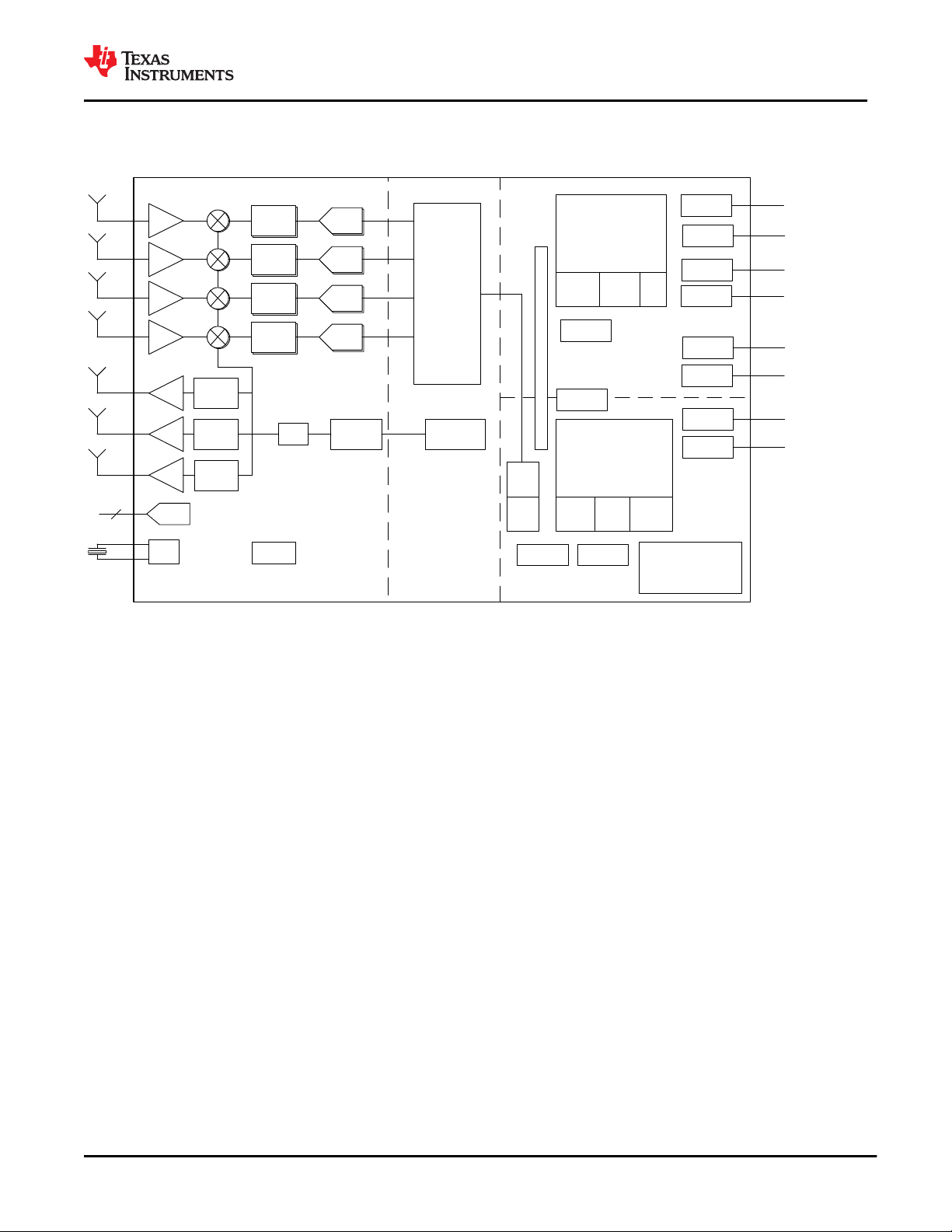
6 Device Comparison
Unless otherwise noted, the device-specific information, in this document, relates to both the IWR6843 and
IWR6443 devices. The device differences are highlighted in Table 6-1, Device Features Comparison.
Table 6-1. Device Features Comparison
FUNCTION IWR6843AOP IWR6843 IWR6443 IWR1843 IWR1642 IWR1443
Antenna on Package (AOP) Yes — — — — —
Number of receivers 4 4 4 4 4 4
Number of transmitters 3
RF frequency range 60 to 64 GHz 60 to 64 GHz 60 to 64 GHz 76 to 81 GHz 76 to 81 GHz 76 to 81 GHz
On-chip memory 1.75MB 1.75MB 1.4MB 2MB 1.5MB 576KB
Max I/F (Intermediate Frequency) (MHz) 10 10 10 10 5 15
Max real sampling rate (Msps) 25 25 25 25 12.5 37.5
Max complex sampling rate (Msps) 12.5 12.5 12.5 12.5 6.25 18.75
SIL — 2-Targeted — — — —
Non-Functional safety variant Yes Yes Yes Yes Yes Yes
Processors
MCU (R4F) Yes Yes Yes Yes Yes Yes
DSP (C674x) Yes Yes — Yes Yes —
Peripherals
Serial Peripheral Interface (SPI) ports 2 2 2 2 2 1
Quad Serial Peripheral Interface (QSPI) Yes Yes Yes Yes Yes Yes
Inter-Integrated Circuit (I2C) interface 1 1 1 1 1 1
Controller Area Network (DCAN) interface — — — Yes Yes Yes
Controller Area Network (CAN-FD) interface Yes Yes Yes Yes — —
Trace Yes Yes Yes Yes Yes —
PWM Yes Yes Yes Yes Yes —
Hardware In Loop (HIL/DMM) Yes Yes Yes Yes Yes —
GPADC Yes Yes Yes Yes Yes Yes
LVDS/Debug Yes Yes Yes Yes Yes Yes
CSI2 — — — — — Yes
Hardware accelerator Yes Yes Yes Yes — Yes
1-V bypass mode Yes Yes Yes Yes Yes Yes
JTAG Yes Yes Yes Yes Yes Yes
Number of Tx that can be simultaneously
used
Product
status
Product Preview (PP),
Advance Information (AI),
or Production Data (PD)
(1)
3 3 3
(2)
AI
PD
(1)
3
(3)
PD
(1)
3
(3)
PD
(1)
3
3
(3)
2 3
2 2
(3)
PD
PD
(3)
(1) 3 Tx Simultaneous operation is supported only with 1-V LDO bypass and PA LDO disable mode. In this mode, the 1-V supply needs to
be fed on the VOUT PA pin.
(2) ADVANCE INFORMATION for pre-production products; subject to change without notice.
(3) PRODUCTION DATA information is current as of publication date. Products conform to specifications per the terms of the Texas
Instruments standard warranty.
6 Submit Document Feedback
Copyright © 2020 Texas Instruments Incorporated
Product Folder Links: IWR6843 IWR6443

www.ti.com
SWRS219D – OCTOBER 2018 – REVISED SEPTEMBER 2020
IWR6843, IWR6443
6.1 Related Products
For information about other devices in this family of products or related products see the links that follow.
mmWave sensors TI’s mmWave sensors rapidly and accurately sense range, angle and velocity with less
power using the smallest footprint mmWave sensor portfolio for industrial applications.
mmWave IWR The Texas Instruments IWRxxxx family of mmWave Sensors are highly integrated and built
on RFCMOS technology operating in 76- to 81-GHz or 60- to 64-GHz frequency band. The
devices have a closed-loop PLL for precise and linear chirp synthesis, includes a built-in
radio processor (BIST) for RF calibration and safety monitoring. The devices have a very
small-form factor, low power consumption, and are highly accurate. Industrial applications
from long range to ultra short range can be realized using these devices.
Companion
products for
IWR6843
Reference
designs for
IWR6843
Review products that are frequently purchased or used in conjunction with this product.
The IWR6843 TI Designs Reference Design Library is a robust reference design library
spanning analog, embedded processor and connectivity. Created by TI experts to help you
jump-start your system design, all TI Designs include schematic or block diagrams, BOMs,
and design files to speed your time to market. Search and download designs at ti.com/
tidesigns.
Copyright © 2020 Texas Instruments Incorporated
Product Folder Links: IWR6843 IWR6443
Submit Document Feedback
7
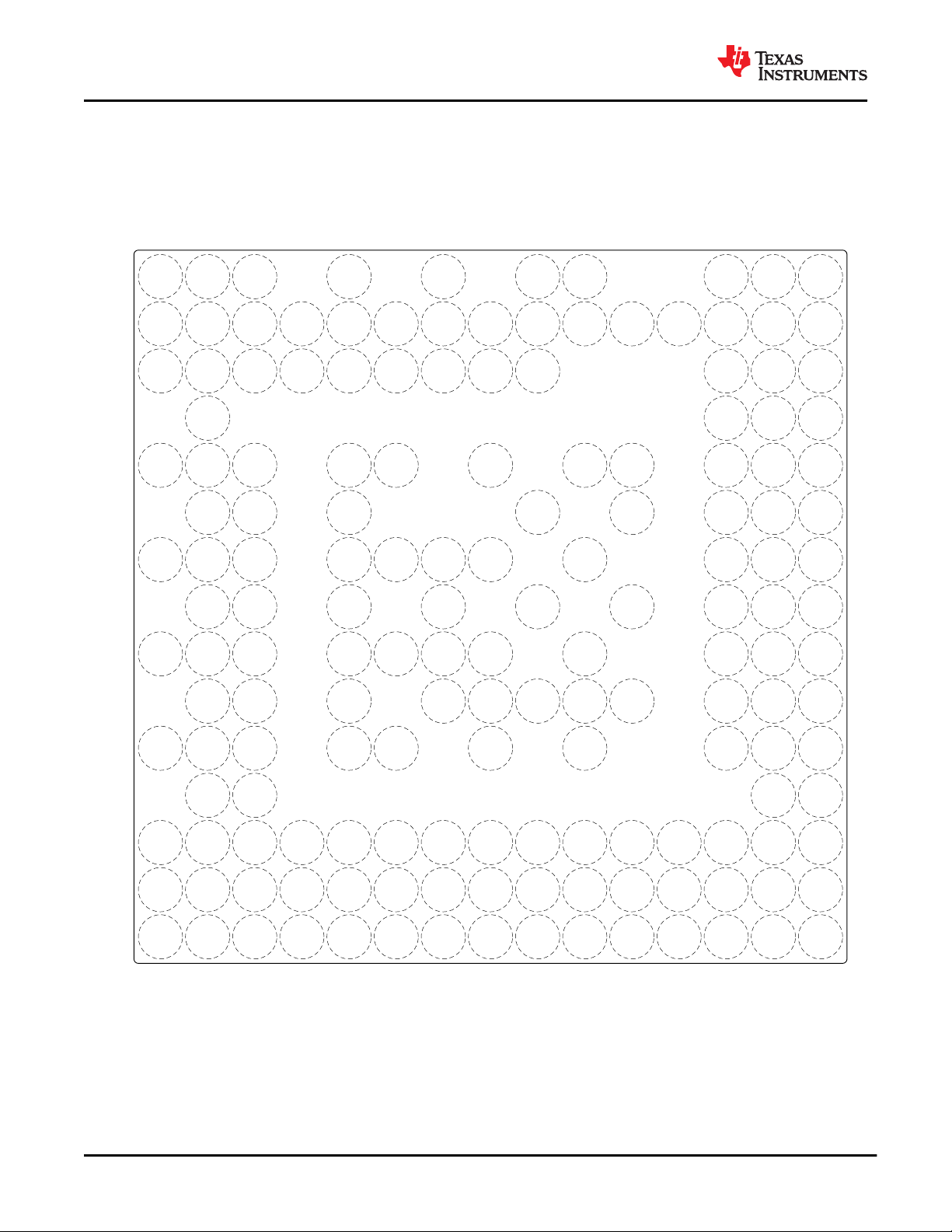
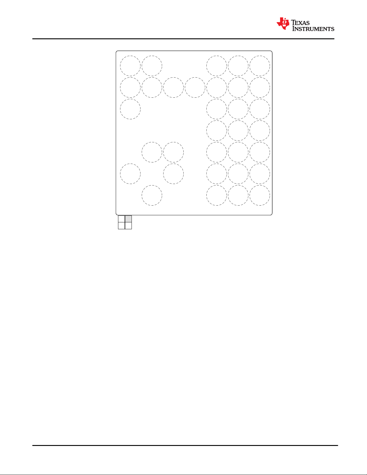
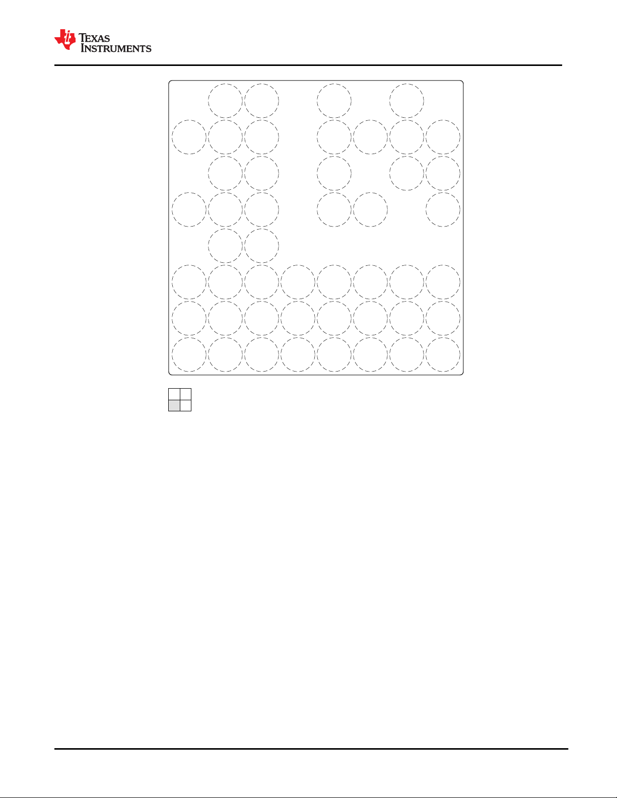
1 2 3 4 5 6 7 8 9 10 11 12 13 14 15
A
B
C
D
E
F
G
H
J
K
L
M
N
P
R
Not to scale
VSSA VOUT_PA VSSA VSSA VSSA
VSSA
VOUT
_14APLL
VSSA
OSC
_CLKOUT
VSSA
VSSA VOUT_PA VSSA TX1 VSSA TX2 VSSA VSSA VBGAP
VIN
_18CLK
VIN
_18VCO
VSSA CLKP
VSSA
VIN
_13RF2
VSSA VSSA VSSA VSSA VSSA
VSSA
VSSA GPADC5 VSSA CLKM
VIN
_13RF2
SPIA_MOSI GPADC6
VSSA VSSA VSSA VSS VSS VSS VSS VSS SPIA_CLK SPIA_MISO
RX4 VSSA VIN_18BB VSS VSS
SPIB_MOSI
VIOIN
VSSA VSSA VSSA
VIN
_13RF1
VSS VSS VSS VSS SYNC_OUT
SPIB_MISO
VIN_SRAM
RX3 VSSA
VIN
_13RF1
VSS VSS VSS GPIO_0 SPIB_CS_N VDDIN
VSSA VSSA VSSA
VIN
_13RF1
VSS VSS VSS VSS GPIO_1 LVDS_TXP[0] LVDS_TXM[0]
RX2 VSSA VIN_18BB VSS VSS VSS VSS VSS GPIO_2 LVDS_TXP[1] LVDS_TXM[1]
VSSA VSSA VSSA VSS VSS VSS VSS VPP LVDS_CLKP LVDS_CLKM
RX1 VSSA
LVDS
_FRCLKP
LVDS
_FRCLKM
VSSA VSSA VSSA RS232_RX RS232_TX NERROR_IN
MCU
_CLKOUT
WARM
_RESET
TMS VDDIN QSPI[1] TDO DMM_SYNC GPIO_47
GPADC1 GPADC2 GPADC3 SYNC_IN GPIO_32
GPIO_34
GPIO_36
GPIO_38
PMIC
_CLKOUT
TCK
QSPI_CS_N
QSPI[3] VNWA VDDIN
VSSA GPADC4 NRESET
GPIO_31
GPIO_33 VDDIN GPIO_35 GPIO_37 VIOIN_18 VIOIN TDI QSPI_CLK QSPI[0] QSPI[2] VSS
VOUT_
14SYNTH
_18VCO
VIOIN_
18DIFF
SPIA_CS_N
SPIB_CLK
SPI_HOST
_INTR
TX3
NERROR
_OUT
IWR6843, IWR6443
SWRS219D – OCTOBER 2018 – REVISED SEPTEMBER 2020
www.ti.com
7 Terminal Configuration and Functions
7.1 Pin Diagram
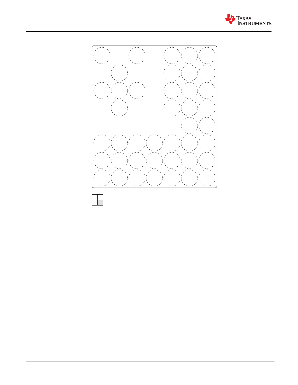
Figure 7-1 shows the pin locations for the 161-pin FCBGA package. Figure 7-2, Figure 7-3, Figure 7-4, and
Figure 7-5 show the same pins, but split into four quadrants.
8 Submit Document Feedback
Figure 7-1. Pin Diagram
Copyright © 2020 Texas Instruments Incorporated
Product Folder Links: IWR6843 IWR6443
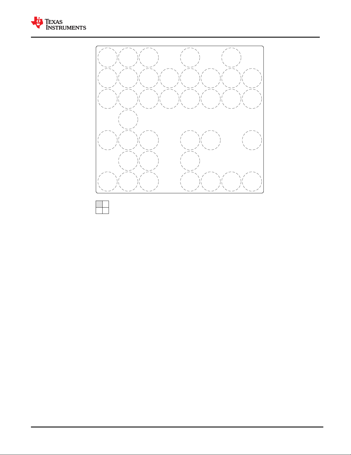
1 2 3 4 5 6 7 8
A
B
C
D
E
F
G
Not to scale
VSSA VOUT_PA VSSA VSSA VSSA
VSSA VOUT_PA VSSA TX1 VSSA TX2 VSSA TX3
VSSA
VIN
_13RF2
VSSA VSSA VSSA VSSA VSSA VSSA
VIN
_13RF2
VSSA VSSA VSSA VSS VSS VSS
RX4 VSSA VIN_18BB
VSSA VSSA VSSA
VIN
_13RF1
VSS VSS VSS
132
4
www.ti.com
SWRS219D – OCTOBER 2018 – REVISED SEPTEMBER 2020
IWR6843, IWR6443
Figure 7-2. Top Left Quadrant
Copyright © 2020 Texas Instruments Incorporated
Product Folder Links: IWR6843 IWR6443
Submit Document Feedback
9
9 10 11 12 13 14 15
A
B
C
D
E
F
G
Not to scale
VSSA
VOUT
_14APLL
VSSA
OSC
_CLKOUT
VSSA
VSSA VBGAP
VIN
_18CLK
VIN
_18VCO
VSSA CLKP
VSSA VSSA CLKM
SPIA_MOSI
VSS VSS
SPIA_CLK
SPIA_MISO
SPIA_CS_N
VSS VSS SPIB_MOSI SPIB_CLK VIOIN
VSS SYNC_OUT SPIB_MISO VIN_SRAM
132
4
VIOIN
_18DIFF
VOUT
_14SYNTH
GPADC5
GPADC6
IWR6843, IWR6443
SWRS219D – OCTOBER 2018 – REVISED SEPTEMBER 2020
www.ti.com
Figure 7-3. Top Right Quadrant
10 Submit Document Feedback
Product Folder Links: IWR6843 IWR6443
Copyright © 2020 Texas Instruments Incorporated
1 2 3 4 5 6 7 8
H
J
K
L
M
N
P
R
Not to scale
RX3 VSSA
VIN
_13RF1
VSS
VSSA VSSA VSSA
VIN
_13RF1
VSS VSS VSS
RX2 VSSA VIN_18BB VSS VSS
VSSA VSSA VSSA VSS VSS VSS
RX1 VSSA
VSSA VSSA VSSA RS232_RX RS232_TX
NERROR
_OUT
NERROR_IN
MCU
_CLKOUT
GPADC1 GPADC2 GPADC3 SYNC_IN GPIO_32 GPIO_34 GPIO_36 GPIO_38
VSSA GPADC4 NRESET GPIO_31 GPIO_33 VDDIN GPIO_35 GPIO_37
132
4
www.ti.com
SWRS219D – OCTOBER 2018 – REVISED SEPTEMBER 2020
IWR6843, IWR6443
Figure 7-4. Bottom Left Quadrant
Copyright © 2020 Texas Instruments Incorporated
Product Folder Links: IWR6843 IWR6443
Submit Document Feedback
11
9 10 11 12 13 14 15
H
J
K
L
M
N
P
R
Not to scale
VSS VSS GPIO_0 SPIB_CS_N VDDIN
VSS GPIO_1 LVDS_TXP[0] LVDS_TXM[0]
VSS VSS VSS GPIO_2 LVDS_TXP[1] LVDS_TXM[1]
VSS VPP LVDS_CLKP LVDS_CLKM
LVDS
_FRCLKP
LVDS
_FRCLKM
WARM
_RESET
TMS VDDIN QSPI[1] TDO DMM_SYNC
GPIO_47
PMIC
_CLKOUT
TCK QSPI_CS_N QSPI[3] VNWA VDDIN
VIOIN_18 VIOIN TDI QSPI_clk QSPI[0] QSPI[2] VSS
132
4
SPI_HOST_
INTR_1
IWR6843, IWR6443
SWRS219D – OCTOBER 2018 – REVISED SEPTEMBER 2020
www.ti.com
Figure 7-5. Bottom Right Quadrant
12 Submit Document Feedback
Product Folder Links: IWR6843 IWR6443
Copyright © 2020 Texas Instruments Incorporated
www.ti.com
SWRS219D – OCTOBER 2018 – REVISED SEPTEMBER 2020
7.2 Pin Attributes
Table 7-1. Pin Attributes (ABL0161 Package)
IWR6843, IWR6443
BALL NUMBER [1] BALL NAME [2] SIGNAL NAME [3]
H13 GPIO_0 GPIO_13 0xFFFFEA04 0 IO Output Disabled Pull Down
GPIO_0 1 IO
PMIC_CLKOUT 2 O
ADC_VALID 9 O
EPWM1B 10 O
ePWM2A 11 O
J13 GPIO_1 GPIO_16 0xFFFFEA08 0 IO Output Disabled Pull Down
GPIO_1 1 IO
SYNC_OUT 2 O
ADC_VALID 7 O
DMM_MUX_IN 12 I
SPIB_CS_N_1 13 IO
SPIB_CS_N_2 14 IO
EPWM1SYNCI 15 I
K13 GPIO_2 GPIO_26 0xFFFFEA64 0 IO Output Disabled Pull Down
GPIO_2 1 IO
OSC_CLKOUT 2 O
MSS_UARTB_TX 7 O
BSS_UART_TX 8 O
SYNC_OUT 9 O
PMIC_CLKOUT 10 O
CHIRP_START 11 O
CHIRP_END 12 O
FRAME_START 13 O
R4 GPIO_31 TRACE_DATA_0 0xFFFFEA7C 0 O Output Disabled Pull Down
GPIO_31 1 IO
DMM0 2 I
MSS_UARTA_TX 4 IO
P5 GPIO_32 TRACE_DATA_1 0xFFFFEA80 0 O Output Disabled Pull Down
GPIO_32 1 IO
DMM1 2 I
R5 GPIO_33 TRACE_DATA_2 0xFFFFEA84 0 O Output Disabled Pull Down
GPIO_33 1 IO
DMM2 2 I
P6 GPIO_34 TRACE_DATA_3 0xFFFFEA88 0 O Output Disabled Pull Down
GPIO_34 1 IO
PINCNTL
ADDRESS[4]
MODE [5] [9] TYPE [6]
BALL RESET
STATE [7]
PULL UP/DOWN
TYPE [8]
Copyright © 2020 Texas Instruments Incorporated
Product Folder Links: IWR6843 IWR6443
Submit Document Feedback
13
IWR6843, IWR6443
SWRS219D – OCTOBER 2018 – REVISED SEPTEMBER 2020
Table 7-1. Pin Attributes (ABL0161 Package) (continued)
BALL NUMBER [1] BALL NAME [2] SIGNAL NAME [3]
DMM3 2 I
EPWM3SYNCO 4 O
R7 GPIO_35 TRACE_DATA_4 0xFFFFEA8C 0 O Output Disabled Pull Down
GPIO_35 1 IO
DMM4 2 I
EPWM2SYNCO 4 O
P7 GPIO_36 TRACE_DATA_5 0xFFFFEA90 0 O Output Disabled Pull Down
GPIO_36 1 IO
DMM5 2 I
MSS_UARTB_TX 5 O
R8 GPIO_37 TRACE_DATA_6 0xFFFFEA94 0 O Output Disabled Pull Down
GPIO_37 1 IO
DMM6 2 I
BSS_UART_TX 5 O
P8 GPIO_38 TRACE_DATA_7 0xFFFFEA98 0 O Output Disabled Pull Down
GPIO_38 1 IO
DMM7 2 I
DSS_UART_TX 5 O
N15 GPIO_47 TRACE_CLK 0xFFFFEABC 0 O Output Disabled Pull Down
GPIO_47 1 IO
DMM_CLK 2 I
N14 DMM_SYNC TRACE_CTL 0xFFFFEAC0 0 O Output Disabled Pull Down
DMM_SYNC 2 I
N8 MCU_CLKOUT GPIO_25 0xFFFFEA60 0 IO Output Disabled Pull Down
MCU_CLKOUT 1 O
CHIRP_START 2 O
CHIRP_END 6 O
FRAME_START 7 O
EPWM1A 12 O
N7 NERROR_IN NERROR_IN 0xFFFFEA44 0 I Input
N6 NERROR_OUT NERROR_OUT 0xFFFFEA4C 0 O Hi-Z (Open Drain)
P9 PMIC_CLKOUT SOP[2] 0xFFFFEA68 During Power Up I Output Disabled Pull Down
GPIO_27 0 IO
PMIC_CLKOUT 1 O
CHIRP_START 6 O
CHIRP_END 7 O
FRAME_START 8 O
EPWM1B 11 O
EPWM2A 12 O
PINCNTL
ADDRESS[4]
MODE [5] [9] TYPE [6]
BALL RESET
STATE [7]
PULL UP/DOWN
www.ti.com
TYPE [8]
14 Submit Document Feedback
Copyright © 2020 Texas Instruments Incorporated
Product Folder Links: IWR6843 IWR6443
www.ti.com
SWRS219D – OCTOBER 2018 – REVISED SEPTEMBER 2020
Table 7-1. Pin Attributes (ABL0161 Package) (continued)
IWR6843, IWR6443
BALL NUMBER [1] BALL NAME [2] SIGNAL NAME [3]
R13 QSPI[0] GPIO_8 0xFFFFEA2C 0 IO Output Disabled Pull Down
QSPI[0] 1 IO
SPIB_MISO 2 IO
N12 QSPI[1] GPIO_9 0xFFFFEA30 0 IO Output Disabled Pull Down
QSPI[1] 1 I
SPIB_MOSI 2 IO
SPIB_CS_N_2 8 IO
R14 QSPI[2] GPIO_10 0xFFFFEA34 0 IO Output Disabled Pull Down
QSPI[2] 1 I
CAN_FD_TX 8 O
P12 QSPI[3] GPIO_11 0xFFFFEA38 0 IO Output Disabled Pull Down
QSPI[3] 1 I
CAN_FD_RX 8 I
R12 QSPI_CLK GPIO_7 0xFFFFEA3C 0 IO Output Disabled Pull Down
QSPI_CLK 1 O
SPIB_CLK 2 IO
DSS_UART_TX 6 O
P11 QSPI_CS_N GPIO_6 0xFFFFEA40 0 IO Output Disabled Pull Up
QSPI_CS_N 1 O
SPIB_CS_N 2 IO
N4 RS232_RX GPIO_15 0xFFFFEA74 0 IO Input Enabled Pull Up
RS232_RX 1 I
MSS_UARTA_RX 2 I
BSS_UART_TX 6 IO
MSS_UARTB_RX 7 IO
CAN_FD_RX 8 I
I2C_SCL 9 IO
EPWM2A 10 O
EPWM2B 11 O
EPWM3A 12 O
N5 RS232_TX GPIO_14 0xFFFFEA78 0 IO Output Enabled
RS232_TX 1 O
MSS_UARTA_TX 5 IO
MSS_UARTB_TX 6 IO
BSS_UART_TX 7 IO
CAN_FD_TX 10 O
I2C_SDA 11 IO
EPWM1A 12 O
PINCNTL
ADDRESS[4]
MODE [5] [9] TYPE [6]
BALL RESET
STATE [7]
PULL UP/DOWN
TYPE [8]
Copyright © 2020 Texas Instruments Incorporated
Product Folder Links: IWR6843 IWR6443
Submit Document Feedback
15
IWR6843, IWR6443
SWRS219D – OCTOBER 2018 – REVISED SEPTEMBER 2020
Table 7-1. Pin Attributes (ABL0161 Package) (continued)
BALL NUMBER [1] BALL NAME [2] SIGNAL NAME [3]
EPWM1B 13 O
NDMM_EN 14 I
EPWM2A 15 O
E13 SPIA_CLK GPIO_3 0xFFFFEA14 0 IO Output Disabled Pull Up
SPIA_CLK 1 IO
DSS_UART_TX 7 O
E15 SPIA_CS_N GPIO_30 0xFFFFEA18 0 IO Output Disabled Pull Up
SPIA_CS_N 1 IO
E14 SPIA_MISO GPIO_20 0xFFFFEA10 0 IO Output Disabled Pull Up
SPIA_MISO 1 IO
CAN_FD_TX 2 O
D13 SPIA_MOSI GPIO_19 0xFFFFEA0C 0 IO Output Disabled Pull Up
SPIA_MOSI 1 IO
CAN_FD_RX 2 I
DSS_UART_TX 8 O
F14 SPIB_CLK GPIO_5 0xFFFFEA24 0 IO Output Disabled Pull Up
SPIB_CLK 1 IO
MSS_UARTA_RX 2 I
MSS_UARTB_TX 6 O
BSS_UART_TX 7 O
CAN_FD_RX 8 I
H14 SPIB_CS_N GPIO_4 0xFFFFEA28 0 IO Output Disabled Pull Up
SPIB_CS_N 1 IO
MSS_UARTA_TX 2 O
MSS_UARTB_TX 6 O
BSS_UART_TX 7 IO
QSPI_CLK_EXT 8 I
CAN_FD_TX 9 O
G14 SPIB_MISO GPIO_22 0xFFFFEA20 0 IO Output Disabled Pull Up
SPIB_MISO 1 IO
I2C_SCL 2 IO
DSS_UART_TX 6 O
F13 SPIB_MOSI GPIO_21 0xFFFFEA1C 0 IO Output Disabled Pull Up
SPIB_MOSI 1 IO
I2C_SDA 2 IO
P13 SPI_HOST_INTR GPIO_12 0xFFFFEA00 0 IO Output Disabled Pull Down
SPI_HOST_INTR 1 O
ADC_VALID 2 O
SPIB_CS_N_1 6 IO
PINCNTL
ADDRESS[4]
MODE [5] [9] TYPE [6]
BALL RESET
STATE [7]
PULL UP/DOWN
www.ti.com
TYPE [8]
16 Submit Document Feedback
Copyright © 2020 Texas Instruments Incorporated
Product Folder Links: IWR6843 IWR6443
www.ti.com
SWRS219D – OCTOBER 2018 – REVISED SEPTEMBER 2020
Table 7-1. Pin Attributes (ABL0161 Package) (continued)
IWR6843, IWR6443
BALL NUMBER [1] BALL NAME [2] SIGNAL NAME [3]
P4 SYNC_IN GPIO_28 0xFFFFEA6C 0 IO Output Disabled Pull Down
SYNC_IN 1 I
MSS_UARTB_RX 6 IO
DMM_MUX_IN 7 I
SYNC_OUT 9 O
G13 SYNC_OUT SOP[1] 0xFFFFEA70 During Power Up I Output Disabled Pull Down
GPIO_29 0 IO
SYNC_OUT 1 O
DMM_MUX_IN 9 I
SPIB_CS_N_1 10 IO
SPIB_CS_N_2 11 IO
P10 TCK GPIO_17 0xFFFFEA50 0 IO Input Enabled Pull Down
TCK 1 I
MSS_UARTB_TX 2 O
CAN_FD_TX 8 O
R11 TDI GPIO_23 0xFFFFEA58 0 IO Input Enabled Pull Up
TDI 1 I
MSS_UARTA_RX 2 I
N13 TDO SOP[0] 0xFFFFEA5C During Power Up I Output Enabled
GPIO_24 0 IO
TDO 1 O
MSS_UARTA_TX 2 O
MSS_UARTB_TX 6 O
BSS_UART_TX 7 O
NDMM_EN 9 I
N10 TMS GPIO_18 0xFFFFEA54 0 IO Input Enabled Pull Down
TMS 1 I
BSS_UART_TX 2 O
CAN_FD_RX 6 I
N9 WARM_RESET WARM_RESET 0xFFFFEA48 0 IO Hi-Z Input (Open
PINCNTL
ADDRESS[4]
MODE [5] [9] TYPE [6]
BALL RESET
STATE [7]
Drain)
PULL UP/DOWN
TYPE [8]
The following list describes the table column headers:
1. BALL NUMBER: Ball numbers on the bottom side associated with each signal on the bottom.
2. BALL NAME: Mechanical name from package device (name is taken from muxmode 0).
3. SIGNAL NAME: Names of signals multiplexed on each ball (also notice that the name of the ball is the signal name in muxmode 0).
4. PINCNTL ADDRESS: MSS Address for PinMux Control
Copyright © 2020 Texas Instruments Incorporated
Product Folder Links: IWR6843 IWR6443
Submit Document Feedback
17

IWR6843, IWR6443
SWRS219D – OCTOBER 2018 – REVISED SEPTEMBER 2020
www.ti.com
5. MODE: Multiplexing mode number: value written to PinMux Cntl register to select specific Signal name for this Ball number. Mode column has bit
range value.
6. TYPE: Signal type and direction:
• I = Input
• O = Output
• IO = Input or Output
7. BALL RESET STATE: The state of the terminal at power-on reset
8. PULL UP/DOWN TYPE: indicates the presence of an internal pullup or pulldown resistor. Pullup and pulldown resistors can be enabled or disabled
via software.
• Pull Up: Internal pullup
• Pull Down: Internal pulldown
• An empty box means No pull.
9. Pin Mux Control Value maps to lower 4 bits of register.
18 Submit Document Feedback
Copyright © 2020 Texas Instruments Incorporated
Product Folder Links: IWR6843 IWR6443
www.ti.com
SWRS219D – OCTOBER 2018 – REVISED SEPTEMBER 2020
IO MUX registers are available in the MSS memory map and the respective mapping to device pins is as follows:
Table 7-2. PAD IO Control Registers
Default Pin/Ball Name Package Ball /Pin (Address) Pin Mux Config Register
SPI_HOST_INTR P13 0xFFFFEA00
GPIO_0 H13 0xFFFFEA04
GPIO_1 J13 0xFFFFEA08
SPIA_MOSI D13 0xFFFFEA0C
SPIA_MISO E14 0xFFFFEA10
SPIA_CLK E13 0xFFFFEA14
SPIA_CS_N E15 0xFFFFEA18
SPIB_MOSI F13 0xFFFFEA1C
SPIB_MISO G14 0xFFFFEA20
SPIB_CLK F14 0xFFFFEA24
SPIB_CS_N H14 0xFFFFEA28
QSPI[0] R13 0xFFFFEA2C
QSPI[1] N12 0xFFFFEA30
QSPI[2] R14 0xFFFFEA34
QSPI[3] P12 0xFFFFEA38
QSPI_CLK R12 0xFFFFEA3C
QSPI_CS_N P11 0xFFFFEA40
NERROR_IN N7 0xFFFFEA44
WARM_RESET N9 0xFFFFEA48
NERROR_OUT N6 0xFFFFEA4C
TCK P10 0xFFFFEA50
TMS N10 0xFFFFEA54
TDI R11 0xFFFFEA58
TDO N13 0xFFFFEA5C
MCU_CLKOUT N8 0xFFFFEA60
GPIO_2 K13 0xFFFFEA64
PMIC_CLKOUT P9 0xFFFFEA68
SYNC_IN P4 0xFFFFEA6C
SYNC_OUT G13 0xFFFFEA70
RS232_RX N4 0xFFFFEA74
RS232_TX N5 0xFFFFEA78
IWR6843, IWR6443
Copyright © 2020 Texas Instruments Incorporated
Product Folder Links: IWR6843 IWR6443
Submit Document Feedback
19
IWR6843, IWR6443
SWRS219D – OCTOBER 2018 – REVISED SEPTEMBER 2020
Table 7-2. PAD IO Control Registers (continued)
Default Pin/Ball Name Package Ball /Pin (Address) Pin Mux Config Register
GPIO_31 R4 0xFFFFEA7C
GPIO_32 P5 0xFFFFEA80
GPIO_33 R5 0xFFFFEA84
GPIO_34 P6 0xFFFFEA88
GPIO_35 R7 0xFFFFEA8C
GPIO_36 P7 0xFFFFEA90
GPIO_37 R8 0xFFFFEA94
GPIO_38 P8 0xFFFFEA98
GPIO_47 N15 0xFFFFEABC
DMM_SYNC N14 0xFFFFEAC0
The register layout is as follows:
Table 7-3. PAD IO Register Bit Descriptions
BIT FIELD TYPE
31-11 NU RW 0 Reserved
10 SC RW 0 IO slew rate control:
9 PUPDSEL RW 0 Pullup/PullDown Selection
8 PI RW 0 Pull Inhibit/Pull Disable
7 OE_OVERRIDE RW 1 Output Override
6 OE_OVERRIDE_CTRL RW 1 Output Override Control:
5 IE_OVERRIDE RW 0 Input Override
4 IE_OVERRIDE_CTRL RW 0 Input Override Control:
3-0 FUNC_SEL RW 1 Function select for Pin Multiplexing (Refer to the Pin Mux Sheet)
RESET (POWER
ON DEFAULT)
DESCRIPTION
0 = Higher slew rate
1 = Lower slew rate
0 = Pull Down
1 = Pull Up (This field is valid only if Pull Inhibit is set as '0')
0 = Enable
1 = Disable
(A '1' here overrides any o/p manipulation of this IO by any of the peripheral block hardware it is
associated with for example a SPI Chip select)
(A '1' here overrides any i/p value on this IO with a desired value)
www.ti.com
20 Submit Document Feedback
Copyright © 2020 Texas Instruments Incorporated
Product Folder Links: IWR6843 IWR6443
www.ti.com
SWRS219D – OCTOBER 2018 – REVISED SEPTEMBER 2020
7.3 Signal Descriptions
Note
All digital IO pins of the device (except NERROR IN, NERROR_OUT, and WARM_RESET) are nonfailsafe; hence, care needs to be taken that they are not driven externally without the VIO supply being
present to the device.
Note
The GPIO state during the power supply ramp is not ensured. In case the GPIO is used in the
application where the state of the GPIO is critical, even when NRESET is low , a tri-state buffer should
be used to isolate the GPIO output from the radar device and a pull resister used to define the
required state in the application. The NRESET signal to the radar device could be used to control the
output enable (OE) of the tri-state buffer.
7.3.1 Signal Descriptions - Digital
SIGNAL NAME PIN TYPE DESCRIPTION BALL NO.
IWR6843, IWR6443
BSS_UART_TX O Debug UART Transmit [Radar Block]
CAN_FD_RX I CAN FD (MCAN) Receive Signal D13, F14, N10, N4, P12
CAN_FD_TX O CAN FD (MCAN) Transmit Signal E14, H14, N5, P10, R14
DMM0 I Debug Interface (Hardware In Loop) - Data Line R4
DMM1 I Debug Interface (Hardware In Loop) - Data Line P5
DMM2 I Debug Interface (Hardware In Loop) - Data Line R5
DMM3 I Debug Interface (Hardware In Loop) - Data Line P6
DMM4 I Debug Interface (Hardware In Loop) - Data Line R7
DMM5 I Debug Interface (Hardware In Loop) - Data Line P7
DMM6 I Debug Interface (Hardware In Loop) - Data Line R8
DMM7 I Debug Interface (Hardware In Loop) - Data Line P8
DMM_CLK I Debug Interface (Hardware In Loop) - Clock N15
DMM_MUX_IN I
DMM_SYNC I Debug Interface (Hardware In Loop) - Sync N14
DSS_UART_TX O Debug UART Transmit [DSP] D13, E13, G14, P8, R12
EPWM1A O PWM Module 1 - Output A N5, N8
EPWM1B O PWM Module 1 - Output B H13, N5, P9
EPWM1SYNCI I PWM Module 1 - Sync Input J13
EPWM2A O PWM Module 2- Output A H13, N4, N5, P9
EPWM2B O PWM Module 2 - Output B N4
EPWM2SYNCO O PWM Module 2 - Sync Output R7
EPWM3A O PWM Module 3 - Output A N4
EPWM3SYNCO O PWM Module 3 - Sync Output P6
GPIO_0 IO General-purpose I/O H13
GPIO_1 IO General-purpose I/O J13
GPIO_2 IO General-purpose I/O K13
GPIO_3 IO General-purpose I/O E13
GPIO_4 IO General-purpose I/O H14
GPIO_5 IO General-purpose I/O F14
GPIO_6 IO General-purpose I/O P11
Debug Interface (Hardware In Loop) Mux Select between DMM1 and
DMM2 (Two Instances)
F14, H14, K13, N10, N13,
N4, N5, R8
G13, J13, P4
Copyright © 2020 Texas Instruments Incorporated
Product Folder Links: IWR6843 IWR6443
Submit Document Feedback
21
IWR6843, IWR6443
SWRS219D – OCTOBER 2018 – REVISED SEPTEMBER 2020
SIGNAL NAME PIN TYPE DESCRIPTION BALL NO.
GPIO_7 IO General-purpose I/O R12
GPIO_8 IO General-purpose I/O R13
GPIO_9 IO General-purpose I/O N12
GPIO_10 IO General-purpose I/O R14
GPIO_11 IO General-purpose I/O P12
GPIO_12 IO General-purpose I/O P13
GPIO_13 IO General-purpose I/O H13
GPIO_14 IO General-purpose I/O N5
GPIO_15 IO General-purpose I/O N4
GPIO_16 IO General-purpose I/O J13
GPIO_17 IO General-purpose I/O P10
GPIO_18 IO General-purpose I/O N10
GPIO_19 IO General-purpose I/O D13
GPIO_20 IO General-purpose I/O E14
GPIO_21 IO General-purpose I/O F13
GPIO_22 IO General-purpose I/O G14
GPIO_23 IO General-purpose I/O R11
GPIO_24 IO General-purpose I/O N13
GPIO_25 IO General-purpose I/O N8
GPIO_26 IO General-purpose I/O K13
GPIO_27 IO General-purpose I/O P9
GPIO_28 IO General-purpose I/O P4
GPIO_29 IO General-purpose I/O G13
GPIO_30 IO General-purpose I/O C13
GPIO_31 IO General-purpose I/O R4
GPIO_32 IO General-purpose I/O P5
GPIO_33 IO General-purpose I/O R5
GPIO_34 IO General-purpose I/O P6
GPIO_35 IO General-purpose I/O R7
GPIO_36 IO General-purpose I/O P7
GPIO_37 IO General-purpose I/O R8
GPIO_38 IO General-purpose I/O P8
GPIO_47 IO General-purpose I/O N15
I2C_SCL IO I2C Clock G14, N4
I2C_SDA IO I2C Data F13, N5
LVDS_TXP[0] O
LVDS_TXM[0] O J15
LVDS_TXP[1] O
LVDS_TXM[1] O K15
LVDS_CLKP O
LVDS_CLKM O L15
LVDS_FRCLKP O
LVDS_FRCLKM O M15
Differential data Out – Lane 0
Differential data Out – Lane 1
Differential clock Out
Differential Frame Clock
MCU_CLKOUT O Programmable clock given out to external MCU or the processor N8
MSS_UARTA_RX I Master Subsystem - UART A Receive F14, N4, R11
MSS_UARTA_TX O Master Subsystem - UART A Transmit H14, N13, N5, R4
www.ti.com
J14
K14
L14
M14
22 Submit Document Feedback
Copyright © 2020 Texas Instruments Incorporated
Product Folder Links: IWR6843 IWR6443
www.ti.com
SIGNAL NAME PIN TYPE DESCRIPTION BALL NO.
MSS_UARTB_RX IO Master Subsystem - UART B Receive N4, P4
MSS_UARTB_TX O Master Subsystem - UART B Transmit
NDMM_EN I Debug Interface (Hardware In Loop) Enable - Active Low Signal N13, N5
Failsafe input to the device. Nerror output from any other device can
NERROR_IN I
be concentrated in the error signaling monitor module inside the
device and appropriate action can be taken by Firmware
Open drain fail safe output signal. Connected to PMIC/
NERROR_OUT O
Processor/MCU to indicate that some severe criticality fault has
happened. Recovery would be through reset.
PMIC_CLKOUT O Output Clock from IWR6843 device for PMIC H13, K13, P9
QSPI[0] IO QSPI Data Line #0 (Used with Serial Data Flash) R13
QSPI[1] I QSPI Data Line #1 (Used with Serial Data Flash) N12
QSPI[2] I QSPI Data Line #2 (Used with Serial Data Flash) R14
QSPI[3] I QSPI Data Line #3 (Used with Serial Data Flash) P12
QSPI_CLK O QSPI Clock (Used with Serial Data Flash) R12
QSPI_CLK_EXT I QSPI Clock (Used with Serial Data Flash) H14
QSPI_CS_N O QSPI Chip Select (Used with Serial Data Flash) P11
RS232_RX I Debug UART (Operates as Bus Master) - Receive Signal N4
RS232_TX O Debug UART (Operates as Bus Master) - Transmit Signal N5
SOP[0] I Sense On Power - Line#0 N13
SOP[1] I Sense On Power - Line#1 G13
SOP[2] I Sense On Power - Line#2 P9
SPIA_CLK IO SPI Channel A - Clock E13
SPIA_CS_N IO SPI Channel A - Chip Select E15
SPIA_MISO IO SPI Channel A - Master In Slave Out E14
SPIA_MOSI IO SPI Channel A - Master Out Slave In D13
SPIB_CLK IO SPI Channel B - Clock F14, R12
SPIB_CS_N IO SPI Channel B Chip Select (Instance ID 0) H14, P11
SPIB_CS_N_1 IO SPI Channel B Chip Select (Instance ID 1) G13, J13, P13
SPIB_CS_N_2 IO SPI Channel B Chip Select (Instance ID 2) G13, J13, N12
SPIB_MISO IO SPI Channel B - Master In Slave Out G14, R13
SPIB_MOSI IO SPI Channel B - Master Out Slave In F13, N12
SPI_HOST_INTR O Out of Band Interrupt to an external host communicating over SPI P13
SYNC_IN I Low frequency Synchronization signal input P4
SYNC_OUT O Low Frequency Synchronization Signal output G13, J13, K13, P4
TCK I JTAG Test Clock P10
TDI I JTAG Test Data Input R11
TDO O JTAG Test Data Output N13
TMS I JTAG Test Mode Signal N10
TRACE_CLK O Debug Trace Output - Clock N15
TRACE_CTL O Debug Trace Output - Control N14
TRACE_DATA_0 O Debug Trace Output - Data Line R4
TRACE_DATA_1 O Debug Trace Output - Data Line P5
TRACE_DATA_2 O Debug Trace Output - Data Line R5
TRACE_DATA_3 O Debug Trace Output - Data Line P6
TRACE_DATA_4 O Debug Trace Output - Data Line R7
SWRS219D – OCTOBER 2018 – REVISED SEPTEMBER 2020
F14, H14, K13, N13, N5,
P10, P7
N7
N6
IWR6843, IWR6443
Copyright © 2020 Texas Instruments Incorporated
Product Folder Links: IWR6843 IWR6443
Submit Document Feedback
23
IWR6843, IWR6443
SWRS219D – OCTOBER 2018 – REVISED SEPTEMBER 2020
SIGNAL NAME PIN TYPE DESCRIPTION BALL NO.
TRACE_DATA_5 O Debug Trace Output - Data Line P7
TRACE_DATA_6 O Debug Trace Output - Data Line R8
TRACE_DATA_7 O Debug Trace Output - Data Line P8
FRAME_START O Pulse signal indicating the start of each frame N8, K13, P9
CHIRP_START O Pulse signal indicating the start of each chirp N8, K13, P9
CHIRP_END O Pulse signal indicating the end of each chirp N8, K13, P9
ADC_VALID O When high, indicating valid ADC samples P13, H13
WARM_RESET IO
Open drain fail safe warm reset signal. Can be driven from PMIC for
diagnostic or can be used as status signal that the device is going
through reset.
N9
7.3.2 Signal Descriptions - Analog
www.ti.com
INTERFACE SIGNAL NAME
TX1 O Single ended transmitter1 o/p B4
Transmitters
Receivers
Reset NRESET I Power on reset for chip. Active low R3
Reference
Oscillator
Reference clock OSC_CLKOUT O
Bandgap voltage VBGAP O Device's Band Gap Reference Output B10
Power supply
Power supply
TX2 O Single ended transmitter2 o/p B6
TX3 O Single ended transmitter3 o/p B8
RX1 I Single ended receiver1 i/p M2
RX2 I Single ended receiver2 i/p K2
RX3 I Single ended receiver3 i/p H2
RX4 I Single ended receiver4 i/p F2
CLKP I
CLKM I
VDDIN Power 1.2V digital power supply H15, N11, P15, R6
VIN_SRAM Power 1.2V power rail for internal SRAM G15
VNWA Power 1.2V power rail for SRAM array back bias P14
VIOIN Power
VIOIN_18 Power 1.8V supply for CMOS IO R9
VIN_18CLK Power 1.8V supply for clock module B11
VIOIN_18DIFF Power 1.8V supply for LVDS port D15
VPP Power Voltage supply for fuse chain L13
VIN_13RF1 Power
VIN_13RF2 Power 1.3V Analog and RF supply C2,D2
VIN_18BB Power 1.8V Analog base band power supply K5, F5
VIN_18VCO Power 1.8V RF VCO supply B12
VSS Ground Digital ground
PIN
TYPE
DESCRIPTION BALL NO.
In XTAL mode: Differential port for reference crystal
In External clock mode: Single ended input
reference clock port
In XTAL mode: Differential port for reference crystal
In External clock mode: Connect this port to ground
Reference clock output from clocking subsystem
after cleanup PLL (1.4V output voltage swing).
I/O Supply (3.3V or 1.8V): All CMOS I/Os would
operate on this supply
1.3V Analog and RF supply,VIN_13RF1 and
VIN_13RF2 could be shorted on the board
B15
C15
A14
R10, F15
G5, H5, J5
L5, L6, L8, L10, K7,
K8, K9, K10, K11,
J6, J7, J8, J10, H7,
H9, H11, G6, G7,
G8, G10, F9, F11,
E5, E6, E8, E10,
E11, R15
24 Submit Document Feedback
Copyright © 2020 Texas Instruments Incorporated
Product Folder Links: IWR6843 IWR6443
 Loading...