

SampleRequest
ClickHere
50kW
150kW 150kW
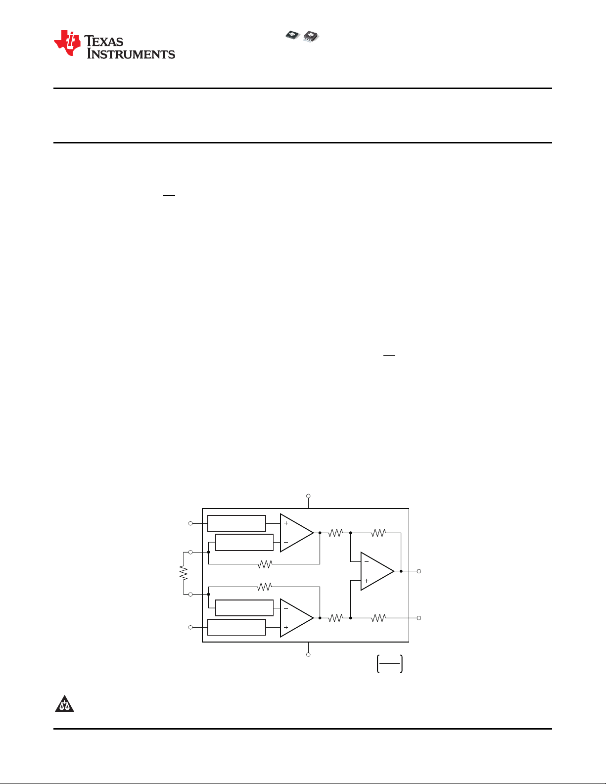
A
1
A
3
V
OUT
V
IN-
6
REF
5
RFIFilteredInputs
2
V+
7
V-
4
1
8
150kW 150kW
50kW
A
2
V
IN+
RFIFilteredInputs
3
INA333
R
G
G=1+
100kW
R
G
RFIFilteredInputs
RFIFilteredInputs
INA333
www.ti.com
...................................................................................................................................................................................................... SBOS445 – JULY 2008
Micro-Power (50 µ A), Zer ø -Drift, Rail-to-Rail Out
Instrumentation Amplifier
1
FEATURES DESCRIPTION
2
• LOW OFFSET VOLTAGE: 25 µ V (max), G ≥ 100
• LOW DRIFT: 0.1 µ V/ ° C, G ≥ 100
• LOW NOISE: 50nV/ √ Hz, G ≥ 100
• HIGH CMRR: 100dB (min), G ≥ 10
• LOW INPUT BIAS CURRENT: 200pA (max)
• SUPPLY RANGE: +1.8V to +5.5V
• INPUT VOLTAGE: (V – ) +0.1V to (V+) – 0.1V
• OUTPUT RANGE: (V – ) +0.05V to (V+) – 0.05V
• LOW QUIESCENT CURRENT: 50 µ A
• OPERATING TEMPERATURE: – 40 ° C to +125 ° C
• RFI FILTERED INPUTS
• MSOP-8 AND DFN-8 PACKAGES
APPLICATIONS
• BRIDGE AMPLIFIERS
• ECG AMPLIFIERS
• PRESSURE SENSORS
• MEDICAL INSTRUMENTATION
• PORTABLE INSTRUMENTATION
• WEIGH SCALES
• THERMOCOUPLE AMPLIFIERS
• RTD SENSOR AMPLIFIERS
• DATA ACQUISITION
The INA333 is a low-power, precision instrumentation
amplifier offering excellent accuracy. The versatile
3-op amp design, small size, and low power make it
ideal for a wide range of portable applications.
A single external resistor sets any gain from 1 to
1000. The INA333 is designed to use an
industry-standard gain equation: G = 1 + (100k Ω /R
The INA333 provides very low offset voltage (25 µ V,
G ≥ 100), excellent offset voltage drift (0.1 µ V/ ° C,
G ≥ 100), and high common-mode rejection (100dB
at G ≥ 10). It operates with power supplies as low as
1.8V ( ± 0.9V), and quiescent current is only
50 µ A — ideal for battery-operated systems. Using
autocalibration techniques to ensure excellent
precision over the extended industrial temperature
range, the INA333 also offers exceptionally low noise
density (50nV/ √ Hz) that extends down to dc.
The INA333 is available in both MSOP-8 and DFN-8
surface-mount packages and is specified over the
TA= – 40 ° C to +125 ° C temperature range.
blank
).
G
1
2 All trademarks are the property of their respective owners.
PRODUCTION DATA information is current as of publication date.
Products conform to specifications per the terms of the Texas
Instruments standard warranty. Production processing does not
necessarily include testing of all parameters.
Please be aware that an important notice concerning availability, standard warranty, and use in critical applications of Texas
Instruments semiconductor products and disclaimers thereto appears at the end of this data sheet.
Copyright © 2008, Texas Instruments Incorporated
V
IN-
V
IN+
V-
R
G
V+
V
OUT
1
2
3
4
8
7
6
5
INA333
R
G
REF
R
G
V
IN-
V
IN+
V-
R
G
V+
V
OUT
REF
1
2
3
4
8
7
6
5
Exposed
Thermal
DiePad
on
Underside
INA333
INA333
SBOS445 – JULY 2008 ......................................................................................................................................................................................................
www.ti.com
This integrated circuit can be damaged by ESD. Texas Instruments recommends that all integrated circuits be handled with
appropriate precautions. Failure to observe proper handling and installation procedures can cause damage.
ESD damage can range from subtle performance degradation to complete device failure. Precision integrated circuits may be more
susceptible to damage because very small parametric changes could cause the device not to meet its published specifications.
PACKAGE/ORDERING INFORMATION
(1)
PRODUCT PACKAGE-LEAD PACKAGE DESIGNATOR PACKAGE MARKING
INA333
MSOP-8 DGK I333
(2)
DFN-8
DRG I333A
(1) For the most current package and ordering information see the Package Option Addendum at the end of this document, or see the TI
web site at www.ti.com .
(2) Available Q4, 2008.
ABSOLUTE MAXIMUM RATINGS
(1)
INA333 UNIT
Supply voltage +7 V
Analog input voltage range
Output short-circuit
Operating temperature range, T
Storage temperature range, T
Junction temperature, T
(2)
(3)
A
A
J
(V – ) – 0.3 to (V+) + 0.3 V
Continuous
– 40 to +150 ° C
– 65 to +150 ° C
+150 ° C
Human body model (HBM) 4000 V
ESD rating Charged device model (CDM) 1000 V
Machine model (MM) 200 V
(1) Stresses above these ratings may cause permanent damage. Exposure to absolute maximum conditions for extended periods may
degrade device reliability. These are stress ratings only, and functional operation of the device at these or any other conditions beyond
those specified is not implied.
(2) Input terminals are diode-clamped to the power-supply rails. Input signals that can swing more than 0.3V beyond the supply rails should
be current limited to 10mA or less.
(3) Short-circuit to ground.
PIN CONFIGURATIONS
DGK PACKAGE
MSOP-8
(TOP VIEW)
2 Submit Documentation Feedback Copyright © 2008, Texas Instruments Incorporated
Product Folder Link(s): INA333
DRG PACKAGE
DFN-8
(TOP VIEW)
INA333
www.ti.com
ELECTRICAL CHARACTERISTICS: V
...................................................................................................................................................................................................... SBOS445 – JULY 2008
= +1.8V to +5.5V
S
Boldface limits apply over the specified temperature range, TA= – 40 ° C to +125 ° C.
At TA= +25 ° C, RL= 10k Ω , V
(1)
INPUT
Offset voltage, RTI
vs Temperature ± 0.1 ± 0.5/G µ V/ ° C
vs Power supply PSR 1.8V ≤ VS≤ 5.5V ± 1 ± 5/G ± 5 ± 15/G µ V/V
Long-term stability See note
Turn-on time to specified V
Impedance
Differential Z
Common-mode Z
Common-mode voltage range V
Common-mode rejection CMR DC to 60Hz
G = 1 VCM= (V – ) + 0.1V to (V+) – 0.1V 80 90 dB
G = 10 VCM= (V – ) + 0.1V to (V+) – 0.1V 100 110 dB
G = 100 VCM= (V – ) + 0.1V to (V+) – 0.1V 100 115 dB
G = 1000 VCM= (V – ) + 0.1V to (V+) – 0.1V 100 115 dB
INPUT BIAS CURRENT
Input bias current I
vs Temperature See Typical Characteristic curve pA/ ° C
Input offset current I
vs Temperature See Typical Characteristic curve pA/ ° C
INPUT VOLTAGE NOISE
Input voltage noise e
f = 10Hz 50 nV/ √ Hz
f = 100Hz 50 nV/ √ Hz
f = 1kHz 50 nV/ √ Hz
f = 0.1Hz to 10Hz 1 µ V
Input current noise i
f = 10Hz 100 fA/ √ Hz
f = 0.1Hz to 10Hz 2 pA
GAIN
Gain equation G 1 + (100k Ω /RG) V/V
Range of gain 1 1000 V/V
Gain error VS= 5.5V, (V – ) + 100mV ≤ VO≤ (V+) – 100mV
G = 1 ± 0.01 ± 0.1 %
G = 10 ± 0.05 ± 0.25 %
G = 100 ± 0.07 ± 0.25 %
G = 1000 ± 0.25 ± 0.5 %
(1) Total VOS, Referred-to-input = (V
(2) RTI = Referred-to-input.
(3) 300-hour life test at +150 ° C demonstrated randomly distributed variation of approximately 1 µ V.
PARAMETER TEST CONDITIONS MIN TYP MAX UNIT
(2)
OSI
= 0, and G = 1, unless otherwise noted.
REF
V
OSI
IN
IN
CM
B
OS
NI
N
) + (V
OSI
/G).
OSO
INA333
± 10 ± 25/G ± 25 ± 75/G µ V
(3)
See Typical characteristics
100 || 3 G Ω || pF
100 || 3 G Ω || pF
VO= 0V (V – ) + 0.1 (V+) – 0.1 V
± 70 ± 200 pA
± 50 ± 200 pA
G = 100, RS= 0 Ω
PP
PP
Copyright © 2008, Texas Instruments Incorporated Submit Documentation Feedback 3
Product Folder Link(s): INA333

INA333
SBOS445 – JULY 2008 ......................................................................................................................................................................................................
ELECTRICAL CHARACTERISTICS: V
= +1.8V to +5.5V (continued)
S
www.ti.com
Boldface limits apply over the specified temperature range, TA= – 40 ° C to +125 ° C.
At TA= +25 ° C, RL= 10k Ω , V
PARAMETER TEST CONDITIONS MIN TYP MAX UNIT
GAIN (continued)
Gain vs Temperature
G = 1 ± 1 ± 5 ppm/ ° C
(4)
G > 1
Gain nonlinearity VS= 5.5V, (V – ) + 100mV ≤ VO≤ (V+) – 100mV
G = 1 to 1000 RL= 10k Ω 10 ppm
OUTPUT
Output voltage swing from rail
Capacitive load drive 500 pF
Short-circuit current I
FREQUENCY RESPONSE
Bandwidth, – 3dB
G = 1 150 kHz
G = 10 35 kHz
G = 100 3.5 kHz
G = 1000 350 Hz
Slew rate SR VS= 5V, VO= 4V Step
G = 1 0.16 V/ µ s
G = 100 0.05 V/ µ s
Settling time to 0.01% t
G = 1 V
G = 100 V
Settling time to 0.001% t
G = 1 V
G = 100 V
Overload recovery 50% overdrive 75 µ s
REFERENCE INPUT
R
IN
Voltage range V – V+ V
POWER SUPPLY
Voltage range
Single +1.8 +5.5 V
Dual ± 0.9 ± 2.75 V
Quiescent current I
vs Temperature 80 µ A
TEMPERATURE RANGE
Specified temperature range – 40 +125 ° C
Operating temperature range – 40 +150 ° C
Thermal resistance θ
MSOP 100 ° C/W
DFN 65 ° C/W
(4) Does not include effects of external resistor RG.
(5) See Typical Characteristics curve, Output Voltage Swing vs Output Current (Figure 29 ).
(5)
= 0, and G = 1, unless otherwise noted.
REF
SC
S
S
Q
JA
INA333
± 15 ± 50 ppm/ ° C
VS= 5.5V, RL= 10k Ω See note
(5)
50 mV
Continuous to common – 40, +5 mA
= 4V 50 µ s
STEP
= 4V 400 µ s
STEP
= 4V 60 µ s
STEP
= 4V 500 µ s
STEP
300 k Ω
VIN= VS/2 50 75 µ A
4 Submit Documentation Feedback Copyright © 2008, Texas Instruments Incorporated
Product Folder Link(s): INA333
-25.0
InputOffsetVoltage( V)m
Population
V =5.5V
S
-2.5
0
2.5
5.0
7.5
10.0
12.5
15.0
17.5
20.0
22.5
-5.0
-7.5
-10.0
-12.5
-15.0
-17.5
-20.0
-22.5
25.0
-0.10
InputVoltageOffsetDrift( V/ C)m °
Population
0.10
V =5.5V
S
-
0.01
0
0.0
1
0.02
0.03
0.04
0.0
5
0.06
0.07
0.08
0.09
- 20.0
- 30.0
- 40.0
- 50.0
- 60.0
- 70.0
- 80.0
- 90.0
-
75.0
OutputOffsetVoltage( V)m
Population
V =5.5V
S
-7.5
0
7.5
15.0
22.5
30.0
37.5
45.0
52.5
60.0
67.5
-15.0
-22.5
-30.0
-37.5
-45.0
-52.5
-60.0
-67.5
75.0
-0.50
OutputVoltageOffsetDrift( V/ C)m °
Population
0.50
V =5.5V
S
-
0.05
0
0.0
5
0.10
0.15
0.20
0.2
5
0.30
0.35
0.40
0.45
-0.10
-0.15
-0.20
- 50.2
-
0.30
-0.35
-0.40
-0.45
Time(1s/div)
Gain=1
Noise(1 V/div)m
0
5
10
15
20
25
-
-
-
-
-
0
0.5
1.0
1.5
V (V)
CM
V ( V)m
OS
5.0
2.0
V =5V
S
3.0 4.02.5 3.5 4.5
V =1.8V
S
INA333
www.ti.com
...................................................................................................................................................................................................... SBOS445 – JULY 2008
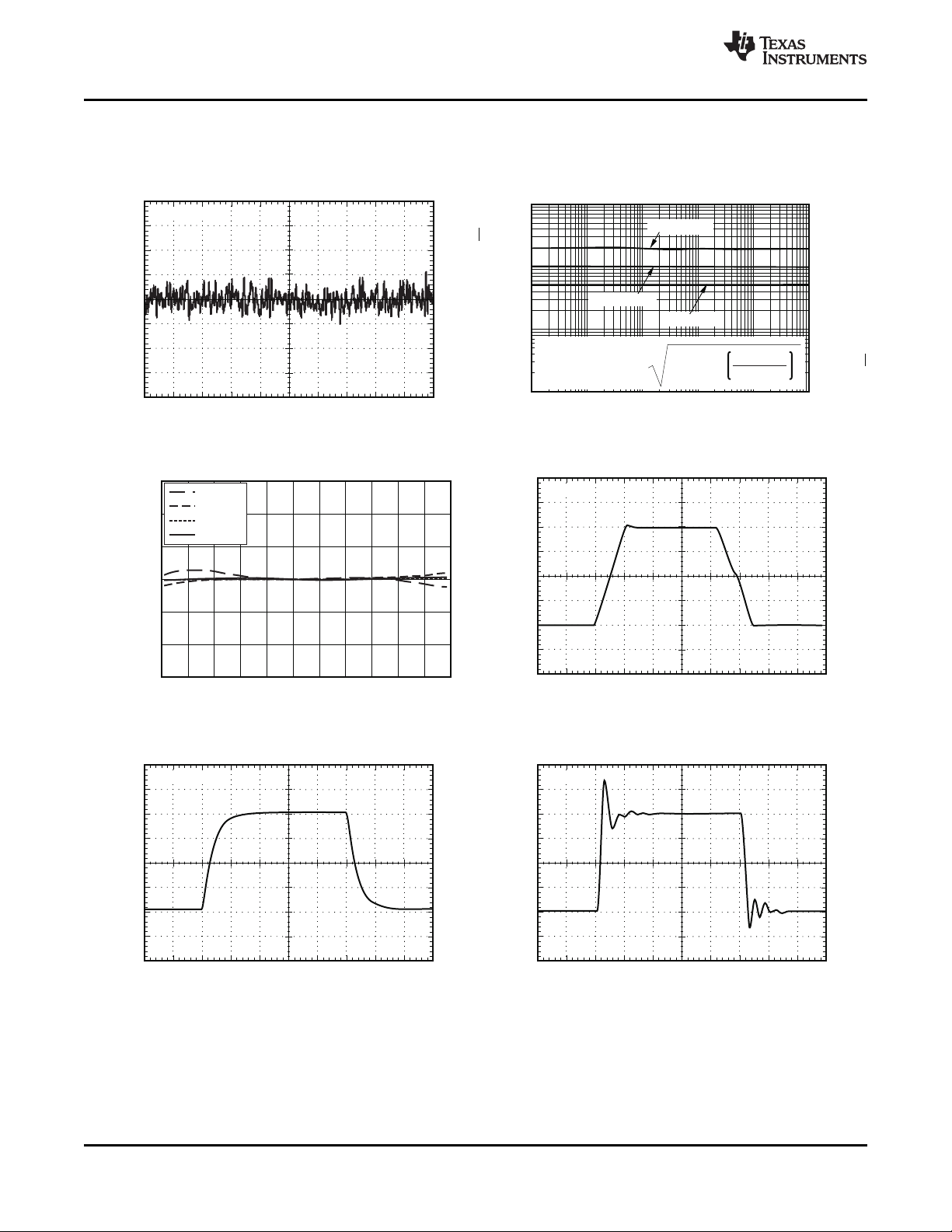
TYPICAL CHARACTERISTICS
At TA= +25 ° C, RL= 10k Ω , V
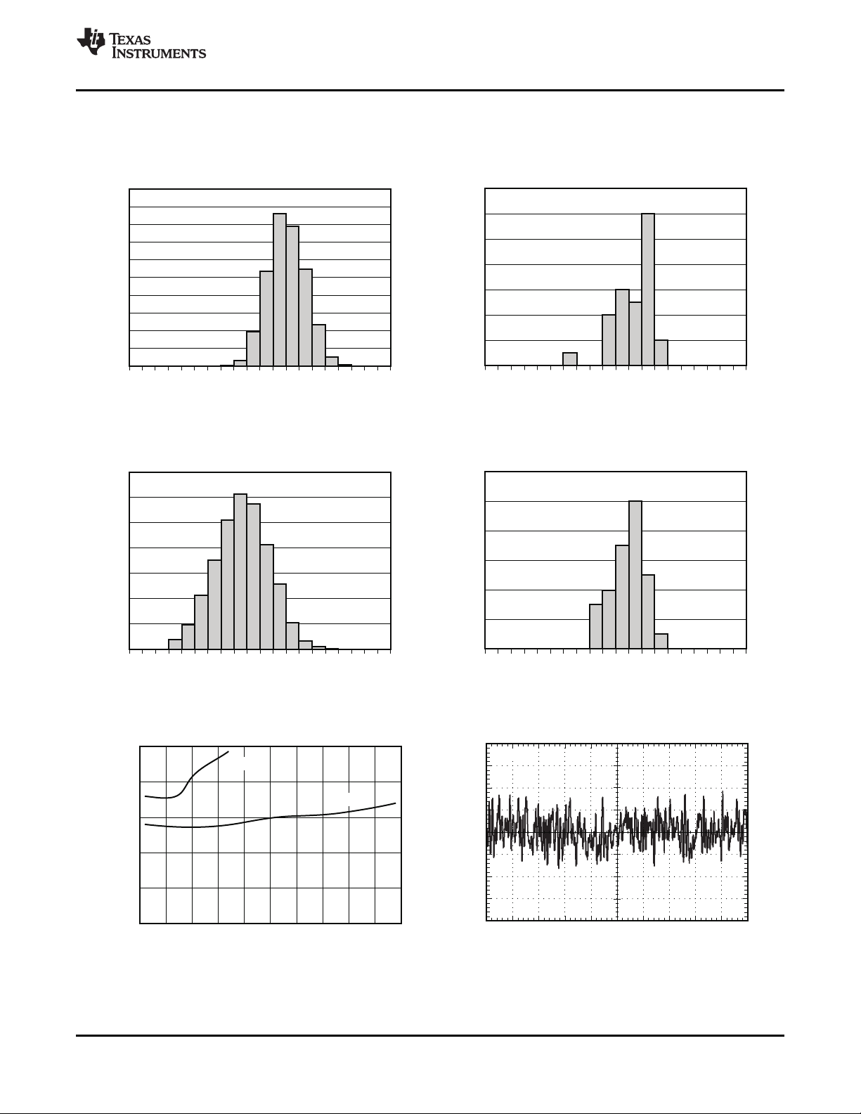
INPUT OFFSET VOLTAGE ( – 40 ° C to +125 ° C)
Figure 1. Figure 2.
OUTPUT OFFSET VOLTAGE ( – 40 ° C to +125 ° C)
= 0, and G = 1, unless otherwise noted.
REF
INPUT VOLTAGE OFFSET DRIFT
OUTPUT VOLTAGE OFFSET DRIFT
Figure 3. Figure 4.
OFFSET VOLTAGE vs COMMON-MODE VOLTAGE 0.1Hz TO 10Hz NOISE
Figure 5. Figure 6.
Copyright © 2008, Texas Instruments Incorporated Submit Documentation Feedback 5
Product Folder Link(s): INA333
Time(1s/div)
Gain=100
Noise(0.5 V/div)m
1000
100
10
1
0.1
1
10
100
1k
Frequency(Hz)
VoltageNoiseDensity(nV/ )
Ö
Hz
10k
CurrentNoise
OutputNoise
InputNoise
TotalInput-ReferredNoise=
(InputNoise) +
2
(OutputNoise)
G
2
1000
100
10
1
CurrentNoiseDensity(f )A/Ö
Hz
Time(25 s/div)m
Gain=1
OutputVoltage(1V/div)
0.012
0.008
0.004
0
0.004
0.008
0.012
-
-
-
0
1.0
V (V)
OUT
DCOutputNonlinearityError(%FSR)
5.5
2.0 3.0 4.0
0.5 1.5 2.5 3.5 4.5 5.0
G=1000
G=100
G=10
G=1
Time(100 s/div)m
Gain=100
OutputVoltage(1V/div)
Time(10 s/div)m
Gain=1
OutputVoltage(50mV/div)
INA333
SBOS445 – JULY 2008 ......................................................................................................................................................................................................
At TA= +25 ° C, RL= 10k Ω , V
0.1Hz TO 10Hz NOISE SPECTRAL NOISE DENSITY
NONLINEARITY ERROR LARGE SIGNAL RESPONSE
TYPICAL CHARACTERISTICS (continued)
= 0, and G = 1, unless otherwise noted.
REF
Figure 7. Figure 8.
www.ti.com
6 Submit Documentation Feedback Copyright © 2008, Texas Instruments Incorporated
Figure 9. Figure 10.
LARGE-SIGNAL STEP RESPONSE SMALL-SIGNAL STEP RESPONSE
Figure 11. Figure 12.
Product Folder Link(s): INA333
Time(100 s/div)m
Gain=100
OutputVoltage(50mV/div)
10000
1000
100
10
1
10
100
Gain(V/V)
Time( s)m
1000
0.01%
0.001%
0.1%
Time(50 s/div)m
Gain=1
Supply(1V/div)
Supply
V
OUT
V (50 V/div)m
OUT
80
60
40
20
0
20
40
60
-
-
-
10
100
1k
10k
Frequency(Hz)
Gain(dB)
1M
G=1
G=1000
G=100
G=10
100k
10
8
6
4
2
0
2
4
6
8
10
-
-
-
-
-
-50
-25
0
25
50
75
100
Temperature( C)°
CMRR(
V/V)
m
G=100,
G=1000
150
V = 2.75V
S
±
V = 0.9V±
S
125
G=1
G=10
-100
CMRR( V/V)m
Population
100
V =5.5V
S
-10
0
10
20
30
40
50
60
70
80
90
-20
-30
-40
-50
-60
-70
-80
-90
INA333
www.ti.com
...................................................................................................................................................................................................... SBOS445 – JULY 2008
At TA= +25 ° C, RL= 10k Ω , V
SMALL-SIGNAL STEP RESPONSE SETTLING TIME vs GAIN
STARTUP SETTLING TIME GAIN vs FREQUENCY
TYPICAL CHARACTERISTICS (continued)
= 0, and G = 1, unless otherwise noted.
REF
Figure 13. Figure 14.
Figure 15. Figure 16.
COMMON-MODE REJECTION RATIO COMMON-MODE REJECTION RATIO vs TEMPERATURE
Copyright © 2008, Texas Instruments Incorporated Submit Documentation Feedback 7
Figure 17. Figure 18.
Product Folder Link(s): INA333

160
140
120
100
80
60
40
20
0
10
100
1k
10k
Frequency(Hz)
CMRR(dB)
100k
G=1
G=1000
G=100
G=10
2.5
-2.5
-2.0
-1.0
0
1.0
2.0
OutputVoltage(V)
Common-ModeV
oltage(V)
2.5
2.0
1.0
0
-1.0
-2.0
2.5
V = 2.5V
V =0
±
S
REF
AllGains
5
4
3
2
1
0
0
1
2
3
4
OutputVoltage(V)
Common-ModeVoltage(V)
5
V =+5V
S
V =0
REF
AllGains
0.9
0.7
0.5
0.3
0.1
0.1
0.3
0.5
0.7
0.9
-
-
-
-
-
-0.9
-0.7
-0.5
-0.3
-0.1
0.1
OutputVoltage(V)
Common-ModeVoltage(V)
0.9
V = 0.9VS±
V =0
REF
0.3 0.5 0.7
AllGains
1.8
1.6
1.4
1.2
1.0
0.8
0.6
0.4
0.2
0
OutputVoltage(V)
Common-ModeV
oltage(V)
0
0.2
0.4
0.5
0.8
1.0
1.81.2 1.4 1.6
AllGains
V =+1.8V
S
V =0
REF
160
140
120
100
80
60
40
20
0
10
100
1k
10k
100k
Frequency(Hz)
+PSRR(dB)
1M
V =5V
S
G=100
G=1000
G=10
G=1
INA333
SBOS445 – JULY 2008 ......................................................................................................................................................................................................
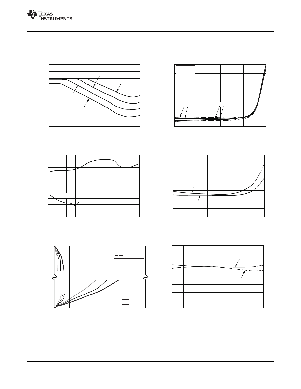
TYPICAL CHARACTERISTICS (continued)
At TA= +25 ° C, RL= 10k Ω , V
COMMON-MODE REJECTION RATIO vs FREQUENCY TYPICAL COMMON-MODE RANGE vs OUTPUT VOLTAGE
TYPICAL COMMON-MODE RANGE vs OUTPUT VOLTAGE TYPICAL COMMON-MODE RANGE vs OUTPUT VOLTAGE
= 0, and G = 1, unless otherwise noted.
REF
Figure 19. Figure 20.
www.ti.com
Figure 21. Figure 22.
TYPICAL COMMON-MODE RANGE vs OUTPUT VOLTAGE POSITIVE POWER-SUPPLY REJECTION RATIO
Figure 23. Figure 24.
8 Submit Documentation Feedback Copyright © 2008, Texas Instruments Incorporated
Product Folder Link(s): INA333
160
140
120
100
80
60
40
20
0
20-
0.1
1
10
100
1k
10k
100k
Frequency(Hz)
-PSRR(dB)
1M
G=1000
V =5V
S
G=100
G=1
G=10
1200
1000
800
600
400
200
0
200-
-50
-25
0
25
50
75
100
Temperature( C)°
I (pA)
B
150
+I
B
-I
B
125
V = 0.9V±
S
V = 2.75V±
S
50
45
40
35
30
25
20
15
10
5
0
0
0.5
1.0
1.5
V (V)
CM
I (pA)
B
5.0
2.0
V =5V
S
3.0 4.02.5 3.5 4.5
V =1.8V
S
250
200
150
100
50
0
50
100--
-50
-25
0
25
50
75
100
Temperature( C)°
I
(pA)
OS
150125
V = 0.9V±
S
V = 2.75V±
S
80
70
60
50
40
30
20
10
0
-50
-25
0
25
50
75
100
Temperature( C)°
I ( A)m
Q
150125
V =5V
S
V =1.8V
S
(V+)
(V+) 0.25(V+) 0.50(V+) 0.75(V+) 1.00(V+) 1.25-
(V )+1.75-
(V )+0.75-
(V )+1.00-
(V )+0.50(V )+0.25-
(V )-
0 10 30 40 50 60
I (mA)
OUT
V (V)
OUT
(V+) 1.75-
(V+) 1.50-
(V )+1.50(V )+1.25-
20
+125 C°
+25 C°
- °40 C
VS= 2.75V±
VS= 0.9V±
INA333
www.ti.com
...................................................................................................................................................................................................... SBOS445 – JULY 2008
At TA= +25 ° C, RL= 10k Ω , V
NEGATIVE POWER-SUPPLY REJECTION RATIO INPUT BIAS CURRENT vs TEMPERATURE
INPUT BIAS CURRENT vs COMMON-MODE VOLTAGE INPUT OFFSET CURRENT vs TEMPERATURE
TYPICAL CHARACTERISTICS (continued)
= 0, and G = 1, unless otherwise noted.
REF
Figure 25. Figure 26.
Figure 27. Figure 28.
OUTPUT VOLTAGE SWING vs OUTPUT CURRENT QUIESCENT CURRENT vs TEMPERATURE
Copyright © 2008, Texas Instruments Incorporated Submit Documentation Feedback 9
Figure 29. Figure 30.
Product Folder Link(s): INA333

80
70
60
50
40
30
20
10
0
0
1.0
V (V)
CM
I ( A)m
Q
5.0
2.0
V =5V
S
3.0 4.0
V =1.8V
S
INA333
SBOS445 – JULY 2008 ......................................................................................................................................................................................................
At TA= +25 ° C, RL= 10k Ω , V
TYPICAL CHARACTERISTICS (continued)
= 0, and G = 1, unless otherwise noted.
REF
QUIESCENT CURRENT vs COMMON-MODE VOLTAGE
www.ti.com
Figure 31.
10 Submit Documentation Feedback Copyright © 2008, Texas Instruments Incorporated
Product Folder Link(s): INA333

A
1
A
2
A
3
6
150kW150kW
150kW150kW
7
4
3
8
1
2
V
IN-
V
IN+
R
G
V+
V-
INA333
G=1+
100kW
R
G
5
RFIFilter
50kW
50kW
RFIFilter
Load
V =G (V´ V- )
O IN+ IN-
0.1 Fm
0.1 Fm
+
-
V
O
R
G
Alsodrawninsimplifiedform:
INA333
Ref
V
O
V
IN-
V
IN+
Ref
RFIFilter
RFIFilter
INA333
www.ti.com
...................................................................................................................................................................................................... SBOS445 – JULY 2008
APPLICATION INFORMATION
Figure 32 shows the basic connections required for Table 1 lists several commonly-used gains and
operation of the INA333. Good layout practice resistor values. The 100k Ω term in Equation 1 comes
mandates the use of bypass capacitors placed close from the sum of the two internal feedback resistors of
to the device pins as shown. A
The output of the INA333 is referred to the output
reference (REF) terminal, which is normally
grounded. This connection must be low-impedance to
assure good common-mode rejection. Although 15 Ω
or less of stray resistance can be tolerated while The stability and temperature drift of the external gain
maintaining specified CMRR, small stray resistances setting resistor, RG, also affects gain. The contribution
of tens of ohms in series with the REF pin can cause of R
noticeable degradation in CMRR. inferred from the gain Equation 1 . Low resistor values
SETTING THE GAIN
Gain of the INA333 is set by a single external
resistor, RG, connected between pins 1 and 8. The
value of R
G = 1 + (100k Ω /R
is selected according to Equation 1 :
G
) (1)
G
and A2. These on-chip resistors are laser trimmed
1
to accurate absolute values. The accuracy and
temperature coefficient of these resistors are included
in the gain accuracy and drift specifications of the
INA333.
to gain accuracy and drift can be directly
G
required for high gain can make wiring resistance
important. Sockets add to the wiring resistance and
contribute additional gain error (possibly an unstable
gain error) in gains of approximately 100 or greater.
To ensure stability, avoid parasitic capacitance of
more than a few picofarads at the R
Careful matching of any parasitics on both R
connections.
G
G
maintains optimal CMRR over frequency.
pins
Copyright © 2008, Texas Instruments Incorporated Submit Documentation Feedback 11
Figure 32. Basic Connections
Product Folder Link(s): INA333

10kW
OPA333
±10mV
AdjustmentRange
100W
100W
100 Am
1/2REF200
100 Am
1/2REF200
V+
V-
R
G
INA333
Ref
V
O
V
IN-
V
IN+
INA333
SBOS445 – JULY 2008 ......................................................................................................................................................................................................
www.ti.com
Table 1. Commonly-Used Gains and Resistor Values
DESIRED GAIN RG( Ω ) NEAREST 1% RG( Ω )
1 NC
2 100k 100k
5 25k 24.9k
10 11.1k 11k
20 5.26k 5.23k
50 2.04k 2.05
100 1.01k 1k
200 502.5 499
500 200.4 200
1000 100.1 100
(1) NC denotes no connection. When using the SPICE model, the simulation will not converge unless a resistor is connected to the RGpins;
use a very large resistor value.
(1)
NC
INTERNAL OFFSET CORRECTION
The INA333 internal op amps use an auto-calibration
technique with a time-continuous 350kHz op amp in
the signal path. The amplifier is zero-corrected every
8 µ s using a proprietary technique. Upon power-up,
the amplifier requires approximately 100 µ s to achieve
specified V
accuracy. This design has no aliasing
OS
or flicker noise.
NOISE PERFORMANCE
The auto-calibration technique used by the INA333
results in reduced low frequency noise, typically only
50nV/ √ Hz, (G = 100). The spectral noise density can
be seen in detail in Figure 8 . Low frequency noise of
the INA333 is approximately 1 µ V
0.1Hz to 10Hz, (G = 100).
PP
measured from
OFFSET TRIMMING
Most applications require no external offset
adjustment; however, if necessary, adjustments can
be made by applying a voltage to the REF terminal.
Figure 33 shows an optional circuit for trimming the
output offset voltage. The voltage applied to REF
terminal is summed at the output. The op amp buffer
provides low impedance at the REF terminal to
preserve good common-mode rejection.
Figure 33. Optional Trimming of Output Offset
Voltage
Product Folder Link(s): INA333
12 Submit Documentation Feedback Copyright © 2008, Texas Instruments Incorporated
INPUT BIAS CURRENT RETURN PATH
The input impedance of the INA333 is extremely
high — approximately 100G Ω . However, a path must
be provided for the input bias current of both inputs.
This input bias current is typically ± 70pA. High input
impedance means that this input bias current
changes very little with varying input voltage.
Input circuitry must provide a path for this input bias
current for proper operation. Figure 34 illustrates
various provisions for an input bias current path.
Without a bias current path, the inputs will float to a
potential that exceeds the common-mode range of
the INA333, and the input amplifiers will saturate. If
the differential source resistance is low, the bias
current return path can be connected to one input
(see the thermocouple example in Figure 34 ). With
higher source impedance, using two equal resistors
provides a balanced input with possible advantages
of lower input offset voltage as a result of bias current
and better high-frequency common-mode rejection.

INA333
47kW47kW
INA333
10kW
Microphone,
Hydrophone,
etc.
Thermocouple
INA333
Centertapprovides
biascurrentreturn.
INA333
www.ti.com
...................................................................................................................................................................................................... SBOS445 – JULY 2008
OPERATING VOLTAGE
The INA333 operates over a power-supply range of
+1.8V to +5.5V ( ± 0.9V to ± 2.75V). Supply voltages
higher than +7V (absolute maximum) can
permanently damage the device. Parameters that
vary over supply voltage or temperature are shown in
the Typical Characteristics section of this data sheet.
LOW VOLTAGE OPERATION
The INA333 can be operated on power supplies as
low as ± 0.9V. Most parameters vary only slightly
throughout this supply voltage range — see the Typical
Characteristics section. Operation at very low supply
voltage requires careful attention to assure that the
input voltages remain within the linear range. Voltage
swing requirements of internal nodes limit the input
common-mode range with low power-supply voltage.
The Typical Characteristic curves Typical
Common-Mode Range vs Output Voltage (Figure 20
to Figure 23 ) show the range of linear operation for
various supply voltages and gains.
SINGLE-SUPPLY OPERATION
The INA333 can be used on single power supplies of
Figure 34. Providing an Input Common-Mode
Current Path
INPUT COMMON-MODE RANGE
The linear input voltage range of the input circuitry of
the INA333 is from approximately 0.1V below the
positive supply voltage to 0.1V above the negative
supply. As a differential input voltage causes the
output voltage to increase, however, the linear input
range is limited by the output voltage swing of
amplifiers A
input range is related to the output voltage of the
complete amplifier. This behavior also depends on
supply voltage — see Typical Characteristic curves
Typical Common-Mode Range vs Output Voltage To illustrate the issues affecting low voltage
(Figure 20 to Figure 23 ). operation, consider the circuit in Figure 35 . It shows
Input overload conditions can produce an output
voltage that appears normal. For example, if an input
overload condition drives both input amplifiers to the
respective positive output swing limit, the difference
voltage measured by the output amplifier is near
zero. The output of the INA333 is near 0V even
though both inputs are overloaded.
and A2. Thus, the linear common-mode
1
+1.8V to +5.5V. Figure 35 illustrates a basic
single-supply circuit. The output REF terminal is
connected to mid-supply. Zero differential input
voltage demands an output voltage of mid-supply.
Actual output voltage swing is limited to
approximately 50mV above ground, when the load is
referred to ground as shown. The typical
characteristic curve Output Voltage Swing vs Output
Current (Figure 29 ) shows how the output voltage
swing varies with output current.
With single-supply operation, V
and V
IN+
be 0.1V above ground for linear operation. For
instance, the inverting input cannot be connected to
ground to measure a voltage connected to the
noninverting input.
the INA333 operating from a single 3V supply. A
resistor in series with the low side of the bridge
assures that the bridge output voltage is within the
common-mode range of the amplifier inputs.
must both
IN –
Copyright © 2008, Texas Instruments Incorporated Submit Documentation Feedback 13
Product Folder Link(s): INA333

300W
+3V
150W
R
(1)
1
2V V- D
2V+ VD
3V
R
G
INA333
V
O
Ref
1.5V
INA333
R /2
G
V
O
LA
RL
RA
10kW
Ref
G=102.8kW
2.8kW
1/2
OPA2333
390kW
390kW
1/2
OPA2333
INA333
SBOS445 – JULY 2008 ......................................................................................................................................................................................................
www.ti.com
GENERAL LAYOUT GUIDELINES
Attention to good layout practices is always
recommended. Keep traces short and, when
possible, use a printed circuit board (PCB) ground
plane with surface-mount components placed as
close to the device pins as possible. Place a 0.1 µ F
bypass capacitor closely across the supply pins.
These guidelines should be applied throughout the
analog circuit to improve performance and provide
benefits such as reducing the
electromagnetic-interference (EMI) susceptibility.
(1) R1creates proper common-mode voltage, only for low-voltage Instrumentation amplifiers vary in the susceptibility to
operation — see the Single-Supply Operation section.
Figure 35. Single-Supply Bridge Amplifier
radio-frequency interference (RFI). RFI can generally
be identified as a variation in offset voltage or dc
signal levels with changes in the interfering RF signal.
The INA333 has been specifically designed to
INPUT PROTECTION
The input terminals of the INA333 are protected with
internal diodes connected to the power-supply rails.
These diodes clamp the applied signal to prevent it
from damaging the input circuitry. If the input signal
voltage can exceed the power supplies by more than
0.3V, the input signal current should be limited to less
than 10mA to protect the internal clamp diodes. This
current limiting can generally be done with a series
input resistor. Some signal sources are inherently
minimize susceptibility to RFI by incorporating RFI
filters at the V
and V
IN+
inputs. As a result, the
IN –
INA333 demonstrates remarkably low sensitivity
compared to previous generation devices. Strong RF
fields may continue to cause varying offset levels,
however, and may require additional shielding.
APPLICATION IDEAS
Additional application ideas are shown in Figure 36 to
Figure 39 .
current-limited and do not require limiting resistors.
Figure 36. ECG Amplifier With Right-Leg Drive
14 Submit Documentation Feedback Copyright © 2008, Texas Instruments Incorporated
Product Folder Link(s): INA333

R
1
100kW
1/2
OPA2333
RA
Inverted
V
CM
+V
S
V
OUT
+V
S
+V
S
+V
S
OPA333
+V
S
1/2V
S
dc
G =1kV/V
TOT
G =200
OPA
f =150Hz
LPF
f =0.5Hz
HPF
(providesacsignalcoupling)
V =+2.7Vto+5.5V
S
BW=0.5Hzto150Hz
f =0.5Hz
O
Wilson
V
CENTRAL
(RA+LA+LL)/3
ac
1/2V
S
R
2
100kW
1/2
OPA2333
LL
+V
S
R
3
100kW
1/2
OPA2333
LA
R
4
100kW
R
9
20kW
R
6
100kW
RL
+V
S
+V
S
1/2
OPA2333
1/2
OPA2333
1/2
OPA2333
INA333
+V
S
3
2
1
4
5
6
G =5
INA
7
C
4
1.06nF
C
3
1 Fm
R
14
1MW
R
12
5kW
R
13
318kW
R
7
100kW
R
8
100kW
R
10
1MW
C
2
0.64 Fm
R
11
1MW
C
1
47pF
R
5
390kW
8
R
G
INA333
www.ti.com
...................................................................................................................................................................................................... SBOS445 – JULY 2008
Copyright © 2008, Texas Instruments Incorporated Submit Documentation Feedback 15
Figure 37. Single-Supply, Very Low Power, ECG Circuit
Product Folder Link(s): INA333

VCC
VCC
Vref+
Vref+
Vref+
Rset 2.5M
VoA2
VoA1
-
+
+
3
1
5
4
2
U5 OPA369
-
+
+
3
1
5
4
2
U6 OPA369
1/2ofmatched
monolithicdual
NPNtransistors
(example:MMDT3904)
Input I10n
uC Vref/2 2.5
V
+
VM1
VCC
VCC
Vref+
Vref+
V1 5
uC Vref/2 2.5
Vdiff
Vout
+
-
+
U1 OPA335
R3 14k
R8 10k
C1 1n
+
RG
RG
V+
V-
Ref
_
Out
2
1
8
3
6
7
5
4 U1 INA333
VCC
1/2ofmatched
monolithicdual
NPNtransistors
(example:MMDT3904)
NOTE: Temperaturecompensation
ofloggingtransistorsisnotshown.
Optionalbufferfordriving
SARconverterswith
samplingsystemsof 33kHz.³
RELATEDPRODUCTS
Formonolithiclogarithmicamplifiers(suchasLOG112orLOG114)seethelinkinfootnote1.
INA333
SBOS445 – JULY 2008 ......................................................................................................................................................................................................
TINA-TI (FREE DOWNLOAD SOFTWARE)
Using TINA-TI SPICE-Based Analog Simulation
Program with the INA333
TINA is a simple, powerful, and easy-to-use circuit
simulation program based on a SPICE engine.
TINA-TI is a free, fully functional version of the TINA
software, preloaded with a library of macromodels in
addition to a range of both passive and active
models. It provides all the conventional dc, transient,
and frequency domain analysis of SPICE as well as
additional design capabilities.
Available as a free download from the Analog eLab
Design Center , TINA-TI offers extensive
post-processing capability that allows users to format
results in a variety of ways.
www.ti.com
Virtual instruments offer users the ability to select
input waveforms and probe circuit nodes, voltages,
and waveforms, creating a dynamic quick-start tool.
Figure 38 and Figure 39 show example TINA-TI
circuits for the INA333 that can be used to develop,
modify, and assess the circuit design for specific
applications. Links to download these simulation files
are given below.
NOTE: these files require that either the TINA
software (from DesignSoft) or TINA-TI software be
installed. Download the free TINA-TI software from
the TINA-TI folder .
(1) The following link launches the TI logarithmic amplifiers web page: Logarithmic Amplifier Products Home Page
To download a compressed file that contains the TINA-TI simulation file for this circuit, click the following link:
Log Circuit .
16 Submit Documentation Feedback Copyright © 2008, Texas Instruments Incorporated
Figure 38. Low-Power Log Function Circuit for Portable Battery-Powered Systems
(Example Glucose Meter)
Product Folder Link(s): INA333

3V
3V
V
REF
3V
V
REF
3V
3V
3V
V
REF
V43
R
2.5k
SET1
W
A
+
I
REF1
+
-
+
U3
OPA333
R
2.5k
SET2
W
A
+
I
REF2
R
2k
1
W
R
100
ZERO
W
RWb
3W
RWc
4W
RWd
3W
RWa
3W
+
-
+
U2
OPA333
C
470nF
7
OUTF
GNDF
OUTS
GNDS
In
EN
U1REF3212
+
-
+
OPA3331OPA333
V
+
VRTD
VT25
VT+
VT-
Mon+ Mon-
RTD+
RTD-
EMU21RTD3
R
100k
GAIN
W
V
DIFF
T3BF256A
T1BF256A
UseBF861A
UseBF861A
G
S
RTDResistance
(Volts=Ohms)
Temp( C)
(Volts= C)°°
Pt100RTD
PGA112
MSP430
V
REF+
+
RG
V+
V-
Ref
_
2
1
8
3
6
7
5
4 U1 INA333
3V
RG
Out
INA333
www.ti.com
...................................................................................................................................................................................................... SBOS445 – JULY 2008
RWa, RWb, RWc, and RWd simulate wire resistance. These resistors are included to show the four-wire sense technique immunity to line
mismatches. This method assumes the use of a four-wire RTD.
Figure 39. Four-Wire, 3V Conditioner for a PT100 RTD With Programmable Gain Acquisition System
To download a compressed file that contains the TINA-TI simulation file for this circuit, click the following link:
PT100 RTD .
Copyright © 2008, Texas Instruments Incorporated Submit Documentation Feedback 17
Product Folder Link(s): INA333

PACKAGE OPTION ADDENDUM
www.ti.com
15-Jul-2008
PACKAGING INFORMATION
Orderable Device Status
(1)
Package
Type
Package
Drawing
Pins Package
Qty
Eco Plan
INA333AIDGKR ACTIVE MSOP DGK 8 2500 Green (RoHS &
no Sb/Br)
INA333AIDGKT ACTIVE MSOP DGK 8 250 Green (RoHS &
no Sb/Br)
INA333AIDRGR PREVIEW SON DRG 8 1000 TBD Call TI Call TI
INA333AIDRGT PREVIEW SON DRG 8 250 TBD Call TI Call TI
(1)
The marketing status values are defined as follows:
ACTIVE: Product device recommended for new designs.
LIFEBUY: TI has announced that the device will be discontinued, and a lifetime-buy period is in effect.
NRND: Not recommended for new designs. Device is in production to support existing customers, but TI does not recommend using this part in
a new design.
PREVIEW: Device has been announced but is not in production. Samples may or may not be available.
OBSOLETE: TI has discontinued the production of the device.
(2)
Eco Plan - The planned eco-friendly classification: Pb-Free (RoHS), Pb-Free (RoHS Exempt), or Green (RoHS & no Sb/Br) - please check
http://www.ti.com/productcontent for the latest availability information and additional product content details.
TBD: The Pb-Free/Green conversion plan has not been defined.
Pb-Free (RoHS): TI's terms "Lead-Free" or "Pb-Free" mean semiconductor products that are compatible with the current RoHS requirements
for all 6 substances, including the requirement that lead not exceed 0.1% by weight in homogeneous materials. Where designed to be soldered
at high temperatures, TI Pb-Free products are suitable for use in specified lead-free processes.
Pb-Free (RoHS Exempt): This component has a RoHS exemption for either 1) lead-based flip-chip solder bumps used between the die and
package, or 2) lead-based die adhesive used between the die and leadframe. The component is otherwise considered Pb-Free (RoHS
compatible) as defined above.
Green (RoHS & no Sb/Br): TI defines "Green" to mean Pb-Free (RoHS compatible), and free of Bromine (Br) and Antimony (Sb) based flame
retardants (Br or Sb do not exceed 0.1% by weight in homogeneous material)
(2)
Lead/Ball Finish MSL PeakTemp
CU NIPDAU Level-2-260C-1 YEAR
CU NIPDAU Level-2-260C-1 YEAR
(3)
(3)
MSL, Peak Temp. -- The Moisture Sensitivity Level rating according to the JEDEC industry standard classifications, and peak solder
temperature.
Important Information and Disclaimer:The information provided on this page represents TI's knowledge and belief as of the date that it is
provided. TI bases its knowledge and belief on information provided by third parties, and makes no representation or warranty as to the
accuracy of such information. Efforts are underway to better integrate information from third parties. TI has taken and continues to take
reasonable steps to provide representative and accurate information but may not have conducted destructive testing or chemical analysis on
incoming materials and chemicals. TI and TI suppliers consider certain information to be proprietary, and thus CAS numbers and other limited
information may not be available for release.
In no event shall TI's liability arising out of such information exceed the total purchase price of the TI part(s) at issue in this document sold by TI
to Customer on an annual basis.
Addendum-Page 1


IMPORTANT NOTICE
Texas Instruments Incorporated and its subsidiaries (TI) reserve the right to make corrections, modifications, enhancements, improvements,
and other changes to its products and services at any time and to discontinue any product or service without notice. Customers should
obtain the latest relevant information before placing orders and should verify that such information is current and complete. All products are
sold subject to TI’s terms and conditions of sale supplied at the time of order acknowledgment.
TI warrants performance of its hardware products to the specifications applicable at the time of sale in accordance with TI’s standard
warranty. Testing and other quality control techniques are used to the extent TI deems necessary to support this warranty. Except where
mandated by government requirements, testing of all parameters of each product is not necessarily performed.
TI assumes no liability for applications assistance or customer product design. Customers are responsible for their products and
applications using TI components. To minimize the risks associated with customer products and applications, customers should provide
adequate design and operating safeguards.
TI does not warrant or represent that any license, either express or implied, is granted under any TI patent right, copyright, mask work right,
or other TI intellectual property right relating to any combination, machine, or process in which TI products or services are used. Information
published by TI regarding third-party products or services does not constitute a license from TI to use such products or services or a
warranty or endorsement thereof. Use of such information may require a license from a third party under the patents or other intellectual
property of the third party, or a license from TI under the patents or other intellectual property of TI.
Reproduction of TI information in TI data books or data sheets is permissible only if reproduction is without alteration and is accompanied
by all associated warranties, conditions, limitations, and notices. Reproduction of this information with alteration is an unfair and deceptive
business practice. TI is not responsible or liable for such altered documentation. Information of third parties may be subject to additional
restrictions.
Resale of TI products or services with statements different from or beyond the parameters stated by TI for that product or service voids all
express and any implied warranties for the associated TI product or service and is an unfair and deceptive business practice. TI is not
responsible or liable for any such statements.
TI products are not authorized for use in safety-critical applications (such as life support) where a failure of the TI product would reasonably
be expected to cause severe personal injury or death, unless officers of the parties have executed an agreement specifically governing
such use. Buyers represent that they have all necessary expertise in the safety and regulatory ramifications of their applications, and
acknowledge and agree that they are solely responsible for all legal, regulatory and safety-related requirements concerning their products
and any use of TI products in such safety-critical applications, notwithstanding any applications-related information or support that may be
provided by TI. Further, Buyers must fully indemnify TI and its representatives against any damages arising out of the use of TI products in
such safety-critical applications.
TI products are neither designed nor intended for use in military/aerospace applications or environments unless the TI products are
specifically designated by TI as military-grade or "enhanced plastic." Only products designated by TI as military-grade meet military
specifications. Buyers acknowledge and agree that any such use of TI products which TI has not designated as military-grade is solely at
the Buyer's risk, and that they are solely responsible for compliance with all legal and regulatory requirements in connection with such use.
TI products are neither designed nor intended for use in automotive applications or environments unless the specific TI products are
designated by TI as compliant with ISO/TS 16949 requirements. Buyers acknowledge and agree that, if they use any non-designated
products in automotive applications, TI will not be responsible for any failure to meet such requirements.
Following are URLs where you can obtain information on other Texas Instruments products and application solutions:
Products Applications
Amplifiers amplifier.ti.com Audio www.ti.com/audio
Data Converters dataconverter.ti.com Automotive www.ti.com/automotive
DSP dsp.ti.com Broadband www.ti.com/broadband
Clocks and Timers www.ti.com/clocks Digital Control www.ti.com/digitalcontrol
Interface interface.ti.com Medical www.ti.com/medical
Logic logic.ti.com Military www.ti.com/military
Power Mgmt power.ti.com Optical Networking www.ti.com/opticalnetwork
Microcontrollers microcontroller.ti.com Security www.ti.com/security
RFID www.ti-rfid.com Telephony www.ti.com/telephony
RF/IF and ZigBee® Solutions www.ti.com/lprf Video & Imaging www.ti.com/video
Mailing Address: Texas Instruments, Post Office Box 655303, Dallas, Texas 75265
Copyright © 2008, Texas Instruments Incorporated
Wireless www.ti.com/wireless
 Loading...