

I
N
A
2
1
7
I
N
A
2
1
7
SBOS247B – JUNE 2002 – REVISED FEBRUARY 2005
Low-Noise, Low-Distortion
INSTRUMENTATION AMPLIFIER
Replacement for SSM2017
INA217
FEATURES
● LOW NOISE: 1.3nV/√Hz at 1kHz
● LOW THD+N: 0.004% at 1kHz, G = 100
● WIDE BANDWIDTH: 800kHz at G = 100
● WIDE SUPPLY RANGE:
±4.5V to ±18V
● HIGH CMR: > 100dB
● GAIN SET WITH EXTERNAL RESISTOR
● DIP-8 AND SOL-16 WIDEBODY PACKAGES
APPLICATIONS
● PROFESSIONAL MICROPHONE PREAMPS
● MOVING-COIL TRANSDUCER AMPLIFIERS
● DIFFERENTIAL RECEIVERS
● BRIDGE TRANSDUCER AMPLIFIERS
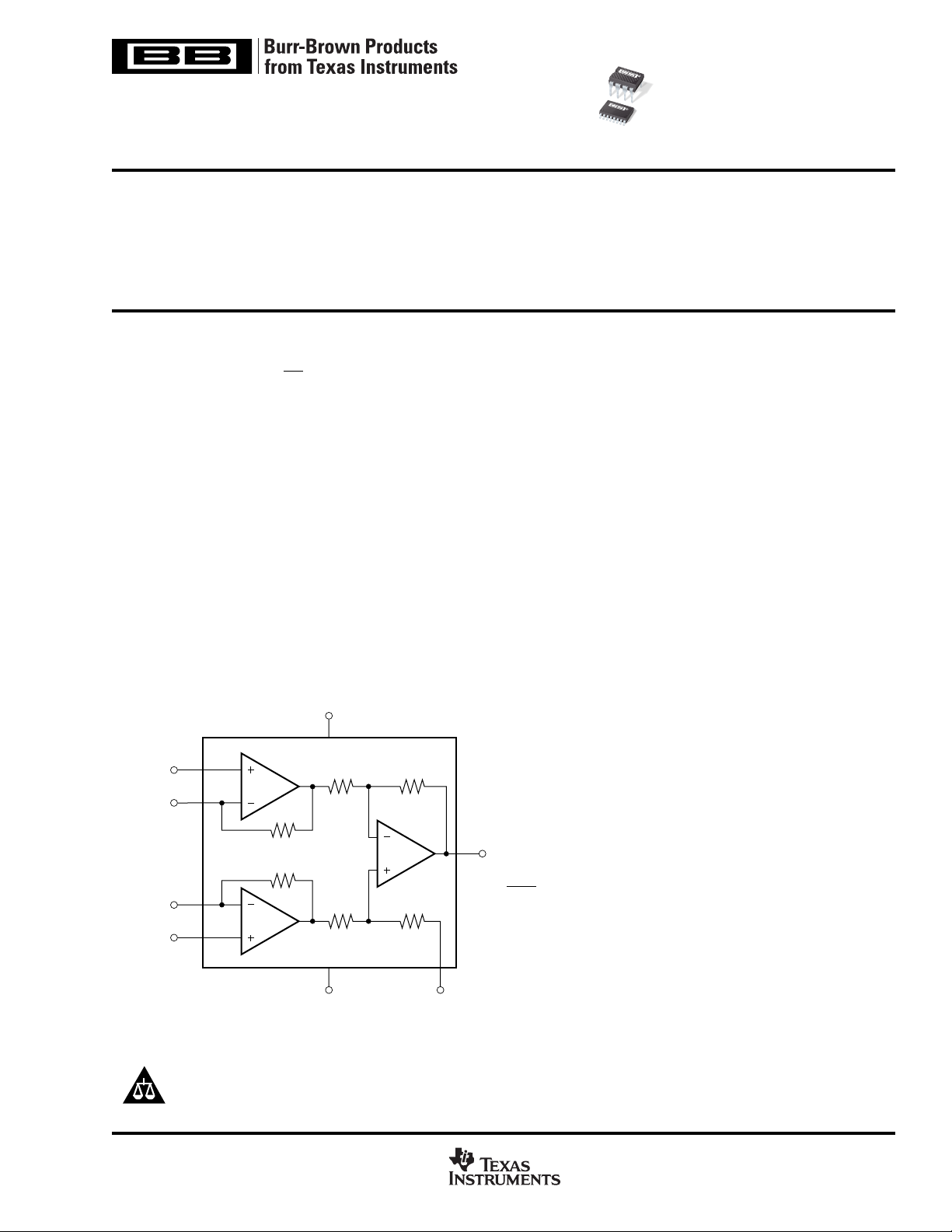
V+
7
INA217
VIN–
RG
2
1
1
A1
5kΩ
6kΩ 6kΩ
DESCRIPTION
The INA217 is a low-noise, low-distortion, monolithic instrumentation amplifier. Current-feedback circuitry allows the
INA217 to achieve wide bandwidth and excellent dynamic
response over a wide range of gain. The INA217 is ideal for
low-level audio signals such as balanced low-impedance
microphones. Many industrial, instrumentation, and medical
applications also benefit from its low noise and wide bandwidth.
Unique distortion cancellation circuitry reduces distortion to
extremely low levels, even in high gain. The INA217 provides
near-theoretical noise performance for 200Ω source impedance. The INA217 features differential input, low noise, and
low distortion that provides superior performance in professional microphone amplifier applications.
The INA217 features wide supply voltage, excellent output
voltage swing, and high output current drive, making it an
optimal candidate for use in high-level audio stages.
The INA217 is available in the same DIP-8 and SOL-16 wide
body packages and pinouts as the SSM2017. For a smaller
package, see the INA163 in SO-14 narrow. The INA217 is
specified over the temperature range of –40°C to +85°C.
5kΩ
8
RG
2
3
VIN+
Please be aware that an important notice concerning availability, standard warranty, and use in critical applications of
Texas Instruments semiconductor products and disclaimers thereto appears at the end of this data sheet.
All trademarks are the property of their respective owners.
PRODUCTION DATA information is current as of publication date.
Products conform to specifications per the terms of Texas Instruments
standard warranty. Production processing does not necessarily include
testing of all parameters.
A2
6kΩ 6kΩ
45
V–
A3
REF
6
V
OUT
10kΩ
G = 1 +
R
www.ti.com
G
Copyright © 2002-2005, Texas Instruments Incorporated
ABSOLUTE MAXIMUM RATINGS
Supply Voltage, V+ to V–.................................................................. ±18V
Signal Input Terminals, Voltage
Output Short-Circuit
Operating Temperature .................................................. –55°C to +125°C
Storage Temperature ..................................................... –55°C to +150°C
Junction Temperature .................................................................... +150°C
Lead Temperature (soldering, 10s)............................................... +300°C
NOTES: (1) Stresses above these ratings may cause permanent damage.
Exposure to absolute maximum conditions for extended periods may degrade
device reliability. (2) Input terminals are diode-clamped to the power-supply
rails. Input signals that can swing more than 0.5V beyond the supply rails
should be current limited to 10mA or less. (3) Short-circuit to ground, one
amplifier per package.
(3)
(2)
.................. (V–) – 0.5V to (V+) + 0.5V
(2)
Current
.............................................................. Continuous
.................................................... 10mA
(1)
ELECTROSTATIC
DISCHARGE SENSITIVITY
This integrated circuit can be damaged by ESD. Texas Instruments recommends that all integrated circuits be handled with
appropriate precautions. Failure to observe proper handling
and installation procedures can cause damage.
ESD damage can range from subtle performance degradation
to complete device failure. Precision integrated circuits may be
more susceptible to damage because very small parametric
changes could cause the device not to meet its published
specifications.
PACKAGE/ORDERING INFORMATION
PRODUCT PACKAGE-LEAD DESIGNATOR MARKING
INA217 SOL-16 DW INA217
INA217 DIP-8 P INA217
NOTES: (1) For the most current package and ordering information, see the
Package Option Addendum at the end of this document, or see the TI website
at www.ti.com.
(1)
PACKAGE PACKAGE
PIN CONFIGURATIONS
Top View
16
NC
15
RG
2
14
NC
13
V+
12
NC
11
V
OUT
10
REF
9
NC
RG
V
V
NC
NC
IN
IN
NC
V–
NC
1
2
1
3
4
–
5
+
6
7
8
RG
VIN–
V
IN
V–
1
1
2
3
+
4
DIP-8
8
RG
2
7
V+
6
V
OUT
5
REF
SOL-16
NC = No Internal Connection
2
www.ti.com
INA217
SBOS247B
ELECTRICAL CHARACTERISTICS: VS = ±15V
Boldface limits apply over the specified temperature range, TA = –40°C to +85°C.
TA = +25°C, RL = 2kΩ, VS = ±15V, unless otherwise noted.
INA217
PARAMETER CONDITIONS MIN TYP MAX UNITS
GAIN EQUATION G = 1 + 10k/R
Range 1 to 10000 V/V
Gain Error, G = 1 ±0.1 ±0.25 %
G = 10 ±0.2 ±0.7 %
G = 100 ±0.2 %
G = 1000 ±0.5 %
Gain Temp Drift Coefficient, G = 1
G > 10
Nonlinearity, G = 1 ±0.0003 % of FS
G = 100 ±0.0006 % of FS
INPUT STAGE NOISE
Voltage Noise R
f
= 1kHz 1.3 nV/
O
fO = 100Hz 1.5 nV/
SOURCE
= 0Ω
fO = 10Hz 3.5 nV/
Current Noise
f
= 1kHz 0.8 pA/
O
OUTPUT STAGE NOISE
Voltage Noise, f
= 1kHz 90 nV/
O
INPUT OFFSET VOLTAGE
Input Offset Voltage V
vs Temperature T
vs Power Supply V
= V
CM
A
= ±4.5V to ±18V 1 + 50/G 3 + 200/G µV/V
S
= 0V 50 + 2000/G 250 + 5000/G µV
OUT
= T
MIN
to T
MAX
1 + 20/G µV/°C
INPUT VOLTAGE RANGE
Common-Mode Voltage Range V
Common-Mode Rejection, G = 1 V
G = 100 100 116 dB
+ – VIN– = 0V (V+) – 4 (V+) – 3V
IN
V
+ – VIN– = 0V (V–) + 4 (V–) + 3 V
IN
= ±11V, R
CM
= 0Ω 70 80 dB
SRC
INPUT BIAS CURRENT
Initial Bias Current 212µA
vs Temperature 10 nA/
Initial Offset Current 0.1 1 µA
vs Temperature 0.5 nA/
INPUT IMPEDANCE
Differential 60 2MΩ pF
Common-Mode 60 2MΩ pF
DYNAMIC RESPONSE
Bandwidth, Small Signal, –3dB, G = 1 3.4 MHz
G = 100 800 kHz
Slew Rate 15 V/µs
THD+Noise, f = 1kHz G = 100 0.004 %
Settling Time, 0.1% G = 100, 10V Step 2 µs
0.01% G = 100, 10V Step 3.5 µs
Overload Recovery 50% Overdrive 1 µs
OUTPUT
Voltage R
to GND (V+) – 2 (V+) – 1.8 V
L
(V–) + 2 (V–) + 1.8 V
Load Capacitance Stability 1000 pF
Short-Circuit Current Continuous-to-Common ±60 mA
POWER SUPPLY
Rated Voltage ±15 V
Voltage Range ±4.5 ±18 V
Current, Quiescent I
= 0mA ±10 ±12 mA
O
TEMPERATURE RANGE
Specification –40 +85 °C
Operating –40 +125 °C
Thermal Resistance
DIP-8
SOL-16 +90 °C/W
NOTE: (1) Gain accuracy is a function of external R
θ
JA
.
G
G
±3 ±10 ppm/°C
±40 ±100 ppm/°C
+85 °C/W
√Hz
√Hz
√Hz
√Hz
√Hz
°C
°C
INA217
SBOS247B
www.ti.com
3
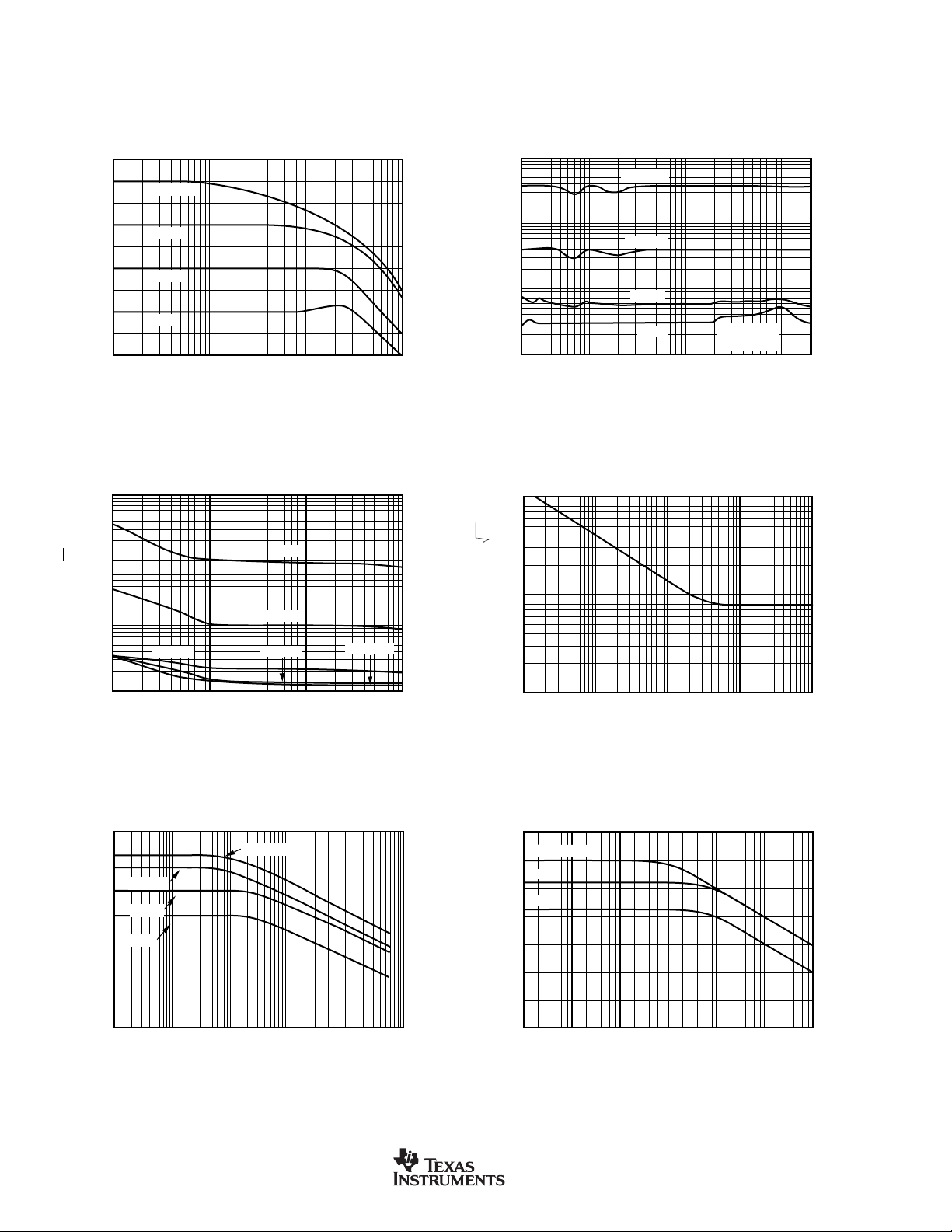
TYPICAL CHARACTERISTICS
At TA = +25°C, VS = ±15V, RL = 2kΩ, unless otherwise noted.
70
60
50
40
30
20
Gain (dB)
10
0
–10
–20
1k
100
10
Noise (RTI) (nV/√Hz)
1
G = 1000
G = 100
G = 10
10k 100k 1M 10M
10 100 1k 10k
GAIN vs FREQUENCY
G = 1
Frequency (Hz)
NOISE VOLTAGE (RTI) vs FREQUENCY
G = 1
G = 10
G = 100
G = 500
Frequency (Hz)
G = 1000
0.1
0.01
THD+N (%)
0.001
0.0001
20 100 1k 10k 20k
10.0
1
Current Noise Density (pA/ Hz)
0.1
1 10 100 1k 10k
THD+N vs FREQUENCY
G = 1000
G = 100
G = 10
G = 1
Frequency (Hz)
CURRENT NOISE SPECTRAL DENSITY
Frequency (Hz)
VO = 7Vrms
R
= 10kΩ
L
140
120
G = 100
100
G = 10
80
G = 1
60
40
Input Referred CMR (dB)
20
0
10 1M
4
CMR vs FREQUENCY
G = 1000
100 1k 10k 100k
Frequency (Hz)
www.ti.com
POWER-SUPPLY REJECTION
140
G = 100, 1000
120
G = 10
100
G = 1
80
60
40
Power-Supply Rejection (dB)
20
0
11M10 100 1k 10k 100k
vs FREQUENCY
Frequency (Hz)
INA217
SBOS247B
TYPICAL CHARACTERISTICS (Cont.)
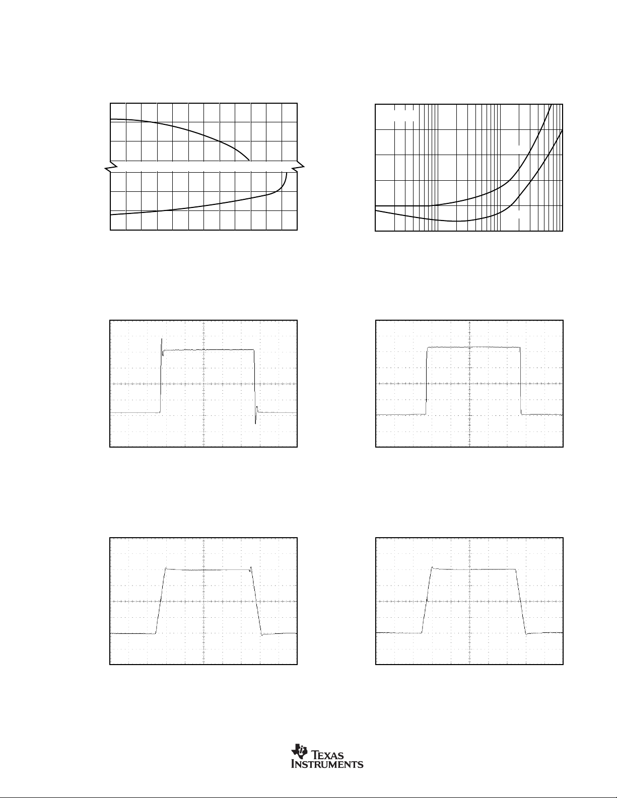
SETTLING TIME vs GAIN
Settling Time (µs)
Gain
1 10 100 1000
10
8
6
4
2
0
20V Step
0.01%
0.1%
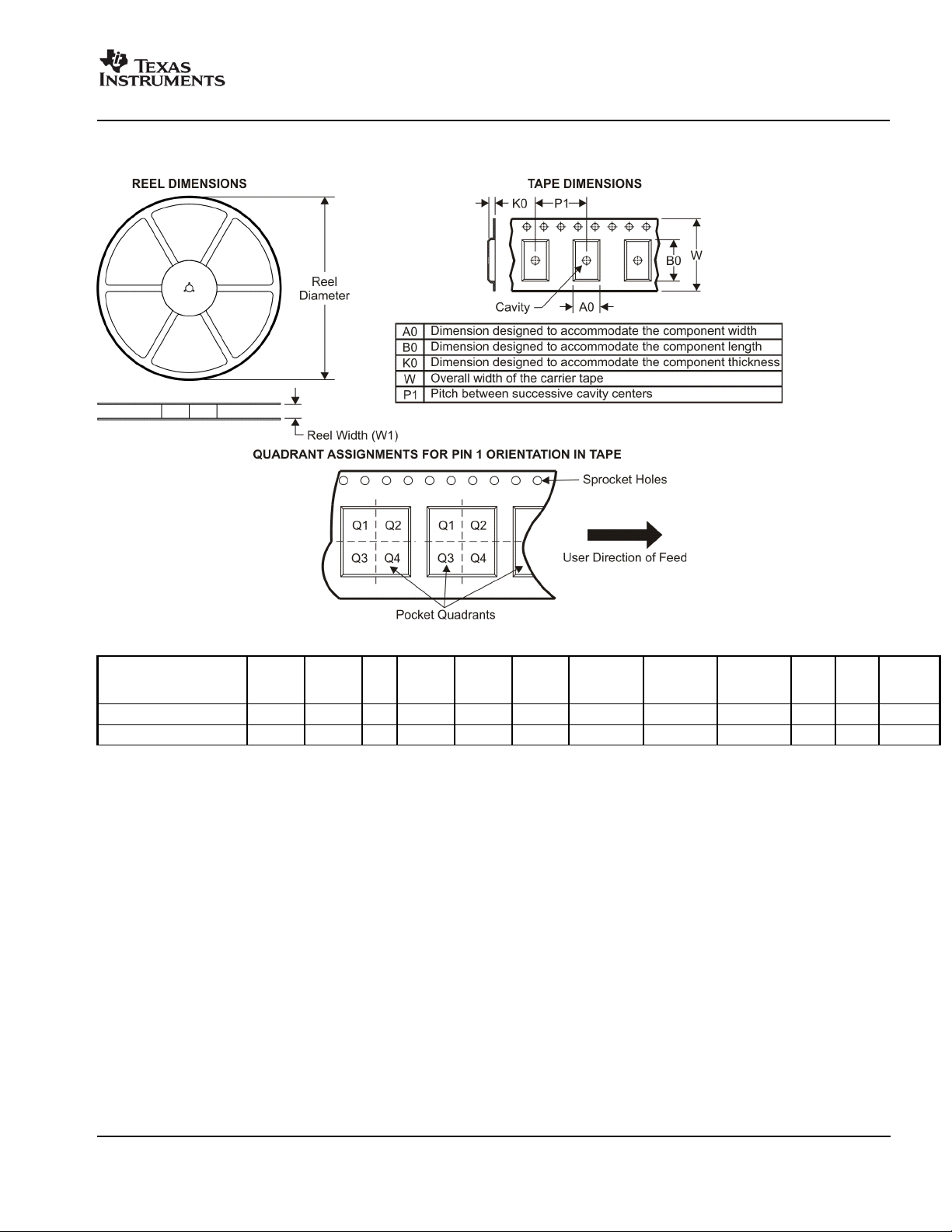
SMALL-SIGNAL TRANSIENT RESPONSE
(G = 100)
20mV/div
10µs/div
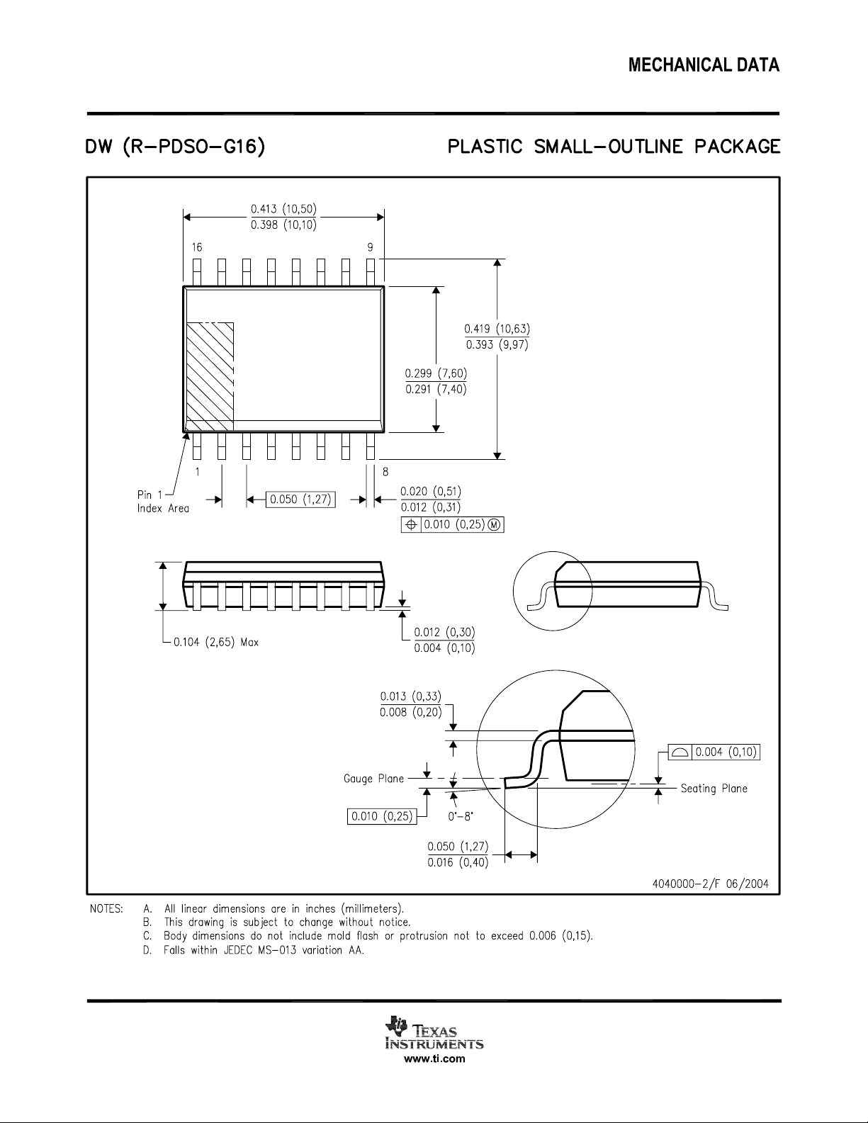
LARGE-SIGNAL TRANSIENT RESPONSE
(G = 100)
5V/div
2.5µs/div
At TA = +25°C, VS = ±15V, RL = 2kΩ, unless otherwise noted.
OUTPUT VOLTAGE SWING vs OUTPUT CURRENT
V+
(V+) – 2
(V+) – 4
(V+) – 6
(V–) + 6
(V–) + 4
Output Voltage to Rail (V)
(V–) + 2
V–
0 102030405060
Output Current (mA)
20mV/div
SMALL-SIGNAL TRANSIENT RESPONSE
(G = 1)
2.5µs/div
LARGE-SIGNAL TRANSIENT RESPONSE
(G = 1)
5V/div
INA217
SBOS247B
2.5µs/div
www.ti.com
5

APPLICATIONS INFORMATION
Figure 1 shows the basic connections required for operation.
Power supplies should be bypassed with 0.1µF tantalum
capacitors near the device pins. The output Reference (pin 5)
should be a low-impedance connection. Resistance of a few
ohms in series with this connection will degrade the common-mode rejection of the INA217.
GAIN-SET RESISTOR
Gain is set with an external resistor, RG, as shown in Figure 1.
The two internal 5kΩ feedback resistors are laser-trimmed to
5kΩ within approximately ±0.2%. The gain equation for the
INA217 is:
=+1
10 000,
R
G
. Avoid
G
.
G
The temperature coefficient of the internal 5kΩ resistors is
approximately ±25ppm/°C. Accuracy and TCR of the external R
will also contribute to gain error and temperature drift.
G
These effects can be inferred from the gain equation. Make
a short, direct connection to the gain set resistor, R
running output signals near these sensitive input nodes
NOISE PERFORMANCE
The INA217 provides very low noise with low-source impedance. Its 1.3nV/
noise performance with a source impedance of 200Ω. The
input stage design used to achieve this low noise results in
√Hz
voltage noise delivers near-theoretical
relatively high input bias current and input bias current noise.
As a result, the INA217 may not provide the best noise
performance with a source impedance greater than 10kΩ.
For source impedance greater than 10kΩ, other instrumentation amplifiers may provide improved noise performance.
INPUT CONSIDERATIONS
Very low source impedance (less than 10Ω) can cause the
INA217 to oscillate. This depends on circuit layout, signal
source, and input cable characteristics. An input network
consisting of a small inductor and resistor, as shown in
Figure 2, can greatly reduce any tendency to oscillate. This
is especially useful if a variety of input sources are to be
connected to the INA217. Although not shown in other
figures, this network can be used as needed with all applications shown.
2
1
8
3
V+
7
INA217
4
V–
6
V
O
5
47Ω
VIN–
V
+
IN
1.2µH
1.2µH
47Ω
FIGURE 2. Input Stabilization Network.
VIN–
V
V+
0.1µF
7
2
–
V
IN
1
R
G
8
V
+
IN
3
V+
Sometimes Shown in
Simplified Form: NOTE: (1) NC = No Connection.
R
INA217
G
+
IN
A1
5kΩ
5kΩ
A2
V
O
6kΩ 6kΩ
6kΩ 6kΩ
INA217
A3
4
0.1µF
V–
6
REF
5
V
G = 1 +
OUT
10000
R
G
GAIN R
(V/V) (dB) (Ω)
10NC
2 6 10000
5 14 2500
10 20 1111
20 26 526
50 34 204
100 40 101
200 46 50
500 54 20
1000 60 10
2000 66 5
G
(1)
V–
FIGURE 1. Basic Circuit Connections.
6
www.ti.com
INA217
SBOS247B

OFFSET VOLTAGE TRIM
A variable voltage applied to pin 5, as shown in Figure 3, can
be used to adjust the output offset voltage. A voltage applied
to pin 5 is summed with the output signal. An op amp
connected as a buffer is used to provide a low impedance at
pin 5 to assure good common-mode rejection.
V+
2
7
1
8
3
INA217
4
V–
R
G
FIGURE 3. Offset Voltage Adjustment Circuit.
5
6
OPA237
V
O
10kΩ
V+
100µA
150Ω
150Ω
100µA
V–
MICROPHONE AMPLIFIER
Figure 4 shows a typical circuit for a professional microphone
input amplifier. R
tional 48V phantom power source for a remotely located
microphone. An optional switch allows phantom power to be
disabled. C
the INA217 input circuitry. Non-polarized capacitors should
be used for C
additional input protection against ESD and hot-plugging,
four IN4148 diodes may be connected from the input to
supply lines.
R
and R5 provide a path for input bias current of the INA217.
4
Input offset current (typically 100nA) creates a DC differential
input voltage that will produce an output offset voltage. This
is generally the dominant source of output offset voltage in
this application. With a maximum gain of 1000 (60dB), the
output offset voltage can be several volts. This may be
entirely acceptable if the output is AC-coupled into the
subsequent stage. An alternate technique is shown in Figure 4.
An inexpensive FET-input op amp in a feedback loop drives
the DC output voltage to 0V. A2 is not in the audio signal path
and does not affect signal quality.
Gain is set with a variable resistor, R
R
determines the maximum gain. The total resistance,
6
R
+ R7, determines the lowest gain. A special reverse-log
6
taper potentiometer for R
change (in dB) with rotation.
and R2 provide a current path for conven-
1
and C2 block the phantom power voltage from
1
and C2 if phantom power is to be disabled. For
1
, in series with R6.
7
can be used to create a linear
7
Phantom Power
+48V
R
1
6.8kΩ
1
Female XLR
Connector
NOTES: (1) Use non-polar capacitors if phantom power is to be
turned off. (2) R
(4) Optional IN4148 prevents damage due to ESD and hot-plugging.
sets maximum gain. (3) R7 sets minimum gain.
6
3
2
R
6.8kΩ
C
47µF
+
C
47µF
+
2
1
60V
2
60V
(1)
(1)
47kΩ
+15V
–15V
R
3
IN4148
+
47µF
+15V
+15V
(2)
R
(4)
R
5
2.2kΩ
6
8Ω
(3)
R
7
1.6kΩ
0.1µF
IN4148
(4)
–15V
R
4
2.2kΩ
7
A1
INA217
4
–15V
0.1µF
5
6
0.1µF
A2
OPA137
V
O
1MΩ
Optional DC
output control loop.
FIGURE 4. Phantom-Powered Microphone Preamplifier.
INA217
SBOS247B
www.ti.com
7
PACKAGE OPTION ADDENDUM
www.ti.com
22-Oct-2007
PACKAGING INFORMATION
Orderable Device Status
(1)
Package
Type
Package
Drawing
Pins Package
Qty
Eco Plan
INA217AIDWR ACTIVE SOIC DW 16 1000 Green (RoHS &
no Sb/Br)
INA217AIDWRE4 ACTIVE SOIC DW 16 1000 Green (RoHS &
no Sb/Br)
INA217AIDWT ACTIVE SOIC DW 16 250 Green (RoHS &
no Sb/Br)
INA217AIDWTE4 ACTIVE SOIC DW 16 250 Green (RoHS &
no Sb/Br)
INA217AIP ACTIVE PDIP P 8 50 Green (RoHS &
no Sb/Br)
INA217AIPG4 ACTIVE PDIP P 8 50 Green (RoHS &
no Sb/Br)
(1)
The marketing status values are defined as follows:
ACTIVE: Product device recommended for new designs.
LIFEBUY: TI has announced that the device will be discontinued, and a lifetime-buy period is in effect.
NRND: Not recommended for new designs. Device is in production to support existing customers, but TI does not recommend using this part in
a new design.
PREVIEW: Device has been announced but is not in production. Samples may or may not be available.
OBSOLETE: TI has discontinued the production of the device.
(2)
Lead/Ball Finish MSL Peak Temp
CU NIPDAU Level-3-260C-168 HR
CU NIPDAU Level-3-260C-168 HR
CU NIPDAU Level-3-260C-168 HR
CU NIPDAU Level-3-260C-168 HR
CU NIPDAU N / A for Pkg Type
CU NIPDAU N / A for Pkg Type
(3)
(2)
Eco Plan - The planned eco-friendly classification: Pb-Free (RoHS), Pb-Free (RoHS Exempt), or Green (RoHS & no Sb/Br) - please check
http://www.ti.com/productcontent for the latest availability information and additional product content details.
TBD: The Pb-Free/Green conversion plan has not been defined.
Pb-Free (RoHS): TI's terms "Lead-Free" or "Pb-Free" mean semiconductor products that are compatible with the current RoHS requirements
for all 6 substances, including the requirement that lead not exceed 0.1% by weight in homogeneous materials. Where designed to be soldered
at high temperatures, TI Pb-Free products are suitable for use in specified lead-free processes.
Pb-Free (RoHS Exempt): This component has a RoHS exemption for either 1) lead-based flip-chip solder bumps used between the die and
package, or 2) lead-based die adhesive used between the die and leadframe. The component is otherwise considered Pb-Free (RoHS
compatible) as defined above.
Green (RoHS & no Sb/Br): TI defines "Green" to mean Pb-Free (RoHS compatible), and free of Bromine (Br) and Antimony (Sb) based flame
retardants (Br or Sb do not exceed 0.1% by weight in homogeneous material)
(3)
MSL, Peak Temp. -- The Moisture Sensitivity Level rating according to the JEDEC industry standard classifications, and peak solder
temperature.
Important Information and Disclaimer:The information provided on this page represents TI's knowledge and belief as of the date that it is
provided. TI bases its knowledge and belief on information provided by third parties, and makes no representation or warranty as to the
accuracy of such information. Efforts are underway to better integrate information from third parties. TI has taken and continues to take
reasonable steps to provide representative and accurate information but may not have conducted destructive testing or chemical analysis on
incoming materials and chemicals. TI and TI suppliers consider certain information to be proprietary, and thus CAS numbers and other limited
information may not be available for release.
In no event shall TI's liability arising out of such information exceed the total purchase price of the TI part(s) at issue in this document sold by TI
to Customer on an annual basis.
Addendum-Page 1
PACKAGE MATERIALS INFORMATION
www.ti.com
TAPE AND REEL INFORMATION
11-Mar-2008
*All dimensions are nominal
Device Package
INA217AIDWR SOIC DW 16 1000 330.0 16.4 10.85 10.8 2.7 12.0 16.0 Q1
INA217AIDWT SOIC DW 16 250 180.0 16.4 10.85 10.8 2.7 12.0 16.0 Q1
Type
Package
Drawing
Pins SPQ Reel
Diameter
(mm)
Reel
Width
W1 (mm)
A0 (mm) B0 (mm) K0 (mm) P1
(mm)W(mm)
Pin1
Quadrant
Pack Materials-Page 1

PACKAGE MATERIALS INFORMATION
www.ti.com
11-Mar-2008
*All dimensions are nominal
Device Package Type Package Drawing Pins SPQ Length (mm) Width (mm) Height (mm)
INA217AIDWR SOIC DW 16 1000 346.0 346.0 33.0
INA217AIDWT SOIC DW 16 250 184.0 184.0 50.0
Pack Materials-Page 2

MECHANICAL DATA
MPDI001A – JANUARY 1995 – REVISED JUNE 1999
P (R-PDIP-T8) PLASTIC DUAL-IN-LINE
0.400 (10,60)
0.355 (9,02)
8
5
0.260 (6,60)
0.240 (6,10)
1
0.021 (0,53)
0.015 (0,38)
NOTES: A. All linear dimensions are in inches (millimeters).
B. This drawing is subject to change without notice.
C. Falls within JEDEC MS-001
4
0.070 (1,78) MAX
0.020 (0,51) MIN
0.200 (5,08) MAX
0.125 (3,18) MIN
0.100 (2,54)
0.010 (0,25)
Seating Plane
M
0.325 (8,26)
0.300 (7,62)
0.015 (0,38)
Gage Plane
0.010 (0,25) NOM
0.430 (10,92)
MAX
4040082/D 05/98
For the latest package information, go to http://www.ti.com/sc/docs/package/pkg_info.htm
POST OFFICE BOX 655303 • DALLAS, TEXAS 75265

IMPORTANT NOTICE
Texas Instruments Incorporated and its subsidiaries (TI) reserve the right to make corrections, modifications, enhancements, improvements,
and other changes to its products and services at any time and to discontinue any product or service without notice. Customers should
obtain the latest relevant information before placing orders and should verify that such information is current and complete. All products are
sold subject to TI’s terms and conditions of sale supplied at the time of order acknowledgment.
TI warrants performance of its hardware products to the specifications applicable at the time of sale in accordance with TI’s standard
warranty. Testing and other quality control techniques are used to the extent TI deems necessary to support this warranty. Except where
mandated by government requirements, testing of all parameters of each product is not necessarily performed.
TI assumes no liability for applications assistance or customer product design. Customers are responsible for their products and
applications using TI components. To minimize the risks associated with customer products and applications, customers should provide
adequate design and operating safeguards.
TI does not warrant or represent that any license, either express or implied, is granted under any TI patent right, copyright, mask work right,
or other TI intellectual property right relating to any combination, machine, or process in which TI products or services are used. Information
published by TI regarding third-party products or services does not constitute a license from TI to use such products or services or a
warranty or endorsement thereof. Use of such information may require a license from a third party under the patents or other intellectual
property of the third party, or a license from TI under the patents or other intellectual property of TI.
Reproduction of TI information in TI data books or data sheets is permissible only if reproduction is without alteration and is accompanied
by all associated warranties, conditions, limitations, and notices. Reproduction of this information with alteration is an unfair and deceptive
business practice. TI is not responsible or liable for such altered documentation. Information of third parties may be subject to additional
restrictions.
Resale of TI products or services with statements different from or beyond the parameters stated by TI for that product or service voids all
express and any implied warranties for the associated TI product or service and is an unfair and deceptive business practice. TI is not
responsible or liable for any such statements.
TI products are not authorized for use in safety-critical applications (such as life support) where a failure of the TI product would reasonably
be expected to cause severe personal injury or death, unless officers of the parties have executed an agreement specifically governing
such use. Buyers represent that they have all necessary expertise in the safety and regulatory ramifications of their applications, and
acknowledge and agree that they are solely responsible for all legal, regulatory and safety-related requirements concerning their products
and any use of TI products in such safety-critical applications, notwithstanding any applications-related information or support that may be
provided by TI. Further, Buyers must fully indemnify TI and its representatives against any damages arising out of the use of TI products in
such safety-critical applications.
TI products are neither designed nor intended for use in military/aerospace applications or environments unless the TI products are
specifically designated by TI as military-grade or "enhanced plastic." Only products designated by TI as military-grade meet military
specifications. Buyers acknowledge and agree that any such use of TI products which TI has not designated as military-grade is solely at
the Buyer's risk, and that they are solely responsible for compliance with all legal and regulatory requirements in connection with such use.
TI products are neither designed nor intended for use in automotive applications or environments unless the specific TI products are
designated by TI as compliant with ISO/TS 16949 requirements. Buyers acknowledge and agree that, if they use any non-designated
products in automotive applications, TI will not be responsible for any failure to meet such requirements.
Following are URLs where you can obtain information on other Texas Instruments products and application solutions:
Products Applications
Amplifiers amplifier.ti.com Audio www.ti.com/audio
Data Converters dataconverter.ti.com Automotive www.ti.com/automotive
DSP dsp.ti.com Broadband www.ti.com/broadband
Clocks and Timers www.ti.com/clocks Digital Control www.ti.com/digitalcontrol
Interface interface.ti.com Medical www.ti.com/medical
Logic logic.ti.com Military www.ti.com/military
Power Mgmt power.ti.com Optical Networking www.ti.com/opticalnetwork
Microcontrollers microcontroller.ti.com Security www.ti.com/security
RFID www.ti-rfid.com Telephony www.ti.com/telephony
RF/IF and ZigBee® Solutions www.ti.com/lprf Video & Imaging www.ti.com/video
Mailing Address: Texas Instruments, Post Office Box 655303, Dallas, Texas 75265
Copyright © 2008, Texas Instruments Incorporated
Wireless www.ti.com/wireless
 Loading...