

Page 1
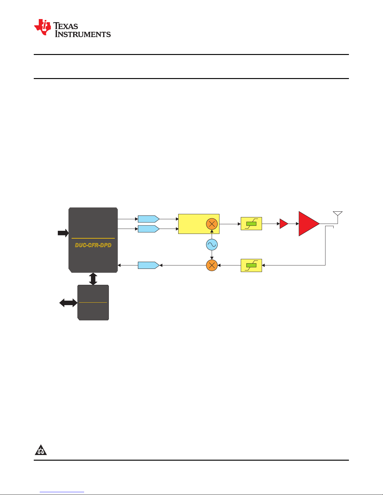
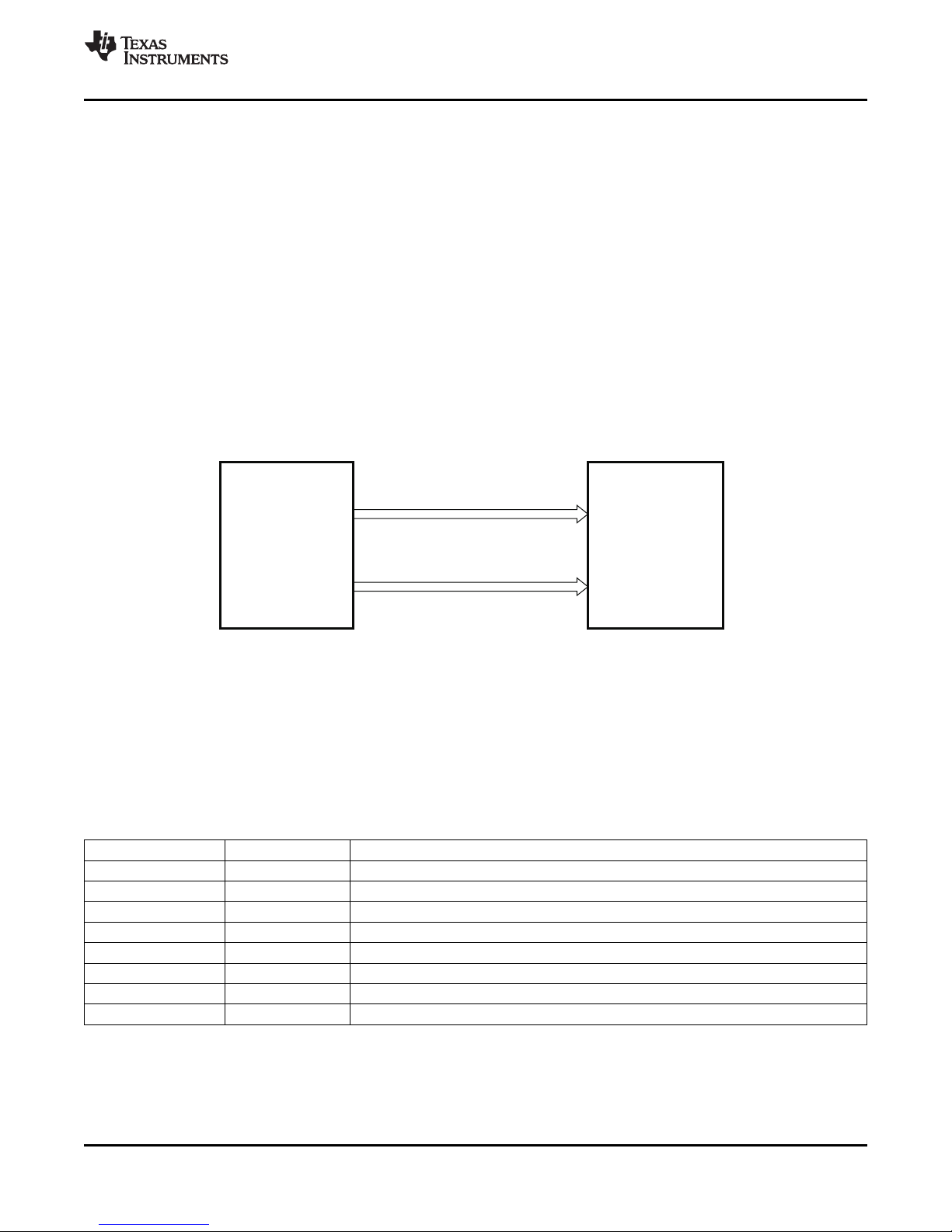
GC5328
DU C- CF R- DP D
BBData
DAC
'C6727
DSP
DAC
I/Q
ADC
I/Q
Modulator
LO
Mixer
LPA
HPA
Attenuator
0 31.5dB–
Attenuator
0 31.5dB–
Host
Control
Interface
B0278-03
GC5328
www.ti.com
SLWS218A –OCTOBER 2009–REVISED OCTOBER 2009
GC5328 Low-Power Wideband Digital Predistortion Transmit Processor
Check for Samples: GC5328
1
FEATURES
• Integrated DUC, CFR, and DPD Solution • Supports Direct Interface to TI High-Speed
• 20-MHz Max. Signal Bandwidth, Based on Max.
DPD Clock of 200 Mhz, Fifth-Order Correction
• DUC: Up to 12 CDMA2000/TDSCDMA, 4
W-CDMA, 2–10 MHz or 1–20 MHz OFDMA
Carriers
• CFR: Typically Meets 3GPP TS 25.141 < 6.5 dB
PAR, < 8.5 dB PAR for OFDMA Signals
• DPD: Short-Term Memory Compensation,
Typical ACLR Improvement > 20 dB
• GC5328IZER PBGA Package, 23 mm × 23 mm
• 1.2-V Core, 1.8-V HSTL, 3.3-V I/O
• 2.5-W Typical Power Consumption
• TMS320C6727 DPD Optimization Software
Data Converters
APPLICATIONS
• 3 GPP (W-CDMA) Base Stations
• 3 GPP2 (CDMA2000) Base Stations
• WiMAX, WiBRO, and LTE (OFDMA) Base
Stations
• Multicarrier Power Amplifiers (MCPAs)
DESCRIPTION
The GC5328 is a lower-power version of the GC5322 wideband digital predistortion transmit processor. The
GC5328 includes a digital upconverter (DUC) block, a crest factor reduction (CFR) block, a digital predistortion
(DPD) block, feedback (FB) block, and capture buffer (CB) blocks.
The GC5328 GPP block receives the interleaved IQ data from the baseband input. The individual IQ channels
are gain-adjusted in the GPP and routed to the DUC. The GPP and DUC can be bypassed to input a combined
IQ signal. The DUC provides three stages of interpolation and a complex mixer. There are two DUC blocks. The
output from the DUC blocks is combined in the sum chain. Each of the 1 to 12 DUC channels can be summed,
and the composite signal can be scaled.
1
Please be aware that an important notice concerning availability, standard warranty, and use in critical applications of Texas
Instruments semiconductor products and disclaimers thereto appears at the end of this data sheet.
PRODUCTION DATA information is current as of publication date.
Products conform to specifications per the terms of the Texas
Instruments standard warranty. Production processing does not
necessarily include testing of all parameters.
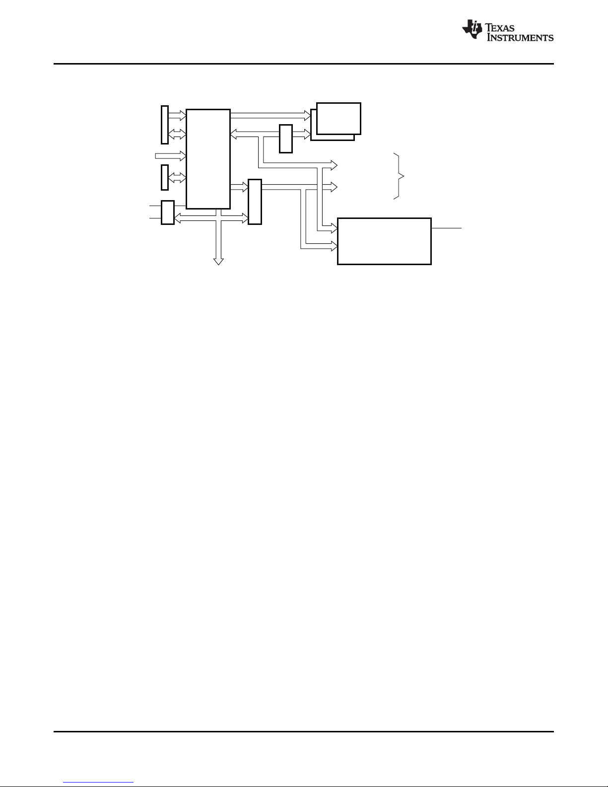
Figure 1. GC5328 System Block Diagram
Copyright © 2009, Texas Instruments Incorporated
Page 2
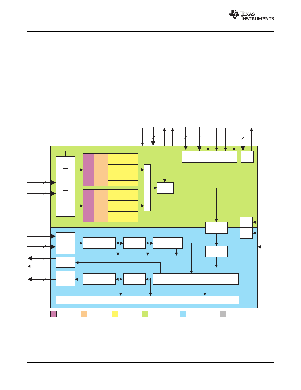
BBin
DACout
Gain
Pilot
Insertion
AntCal
Insertion
Power
Meter
16
BBFR
1
Wide
Band
DUC
Wide
Band
DUC
Medium
Band
DUC
Medium
Band
DUC
Medium
Band
DUC
Medium
Band
DUC
NarrowBand DUC
NarrowBand DUC
NarrowBand DUC
NarrowBand DUC
NarrowBand DUC
NarrowBand DUC
NarrowBand DUC
NarrowBand DUC
NarrowBand DUC
NarrowBand DUC
NarrowBand DUC
NarrowBand DUC
+
CFR
Fractional
Resampler
Circular
Limiter
GC5328
JTAGMPU Interface
RESETB
SYNC3SYNC
OUT
INT UPDATA UPADDR
OEB
RDB WRB
CEB
TCK
TRST
TI
TMS
TD
16
10
4
BBclk
DPDclk
SYNC
BB
PLL
DPD
PLL
Real to Complex
Feedback
Equalizer
Feedback Mixer
and NL Correction
Bulk Interpolation
+ Mixer
Transmit
Equalizer
DPD
ADC
Interface
DAC
Interface
Capture Buffers
DUCs in
1-Chn Mode
DUCs in
2-Chn Mode
DUCs in
6-Chn Mode
BB Clock Domain DPD Clock Domain
B0279-03
Envelope
Interface
To Capture
Buffer
To Capture
Buffer
To Capture
Buffer
Pilot
Insertion
ADCin
(LVDS)
16
ADCin
(LVDS)
2
16
MAGclk
MAGout
38
Active Only in Dual
Antenna Mode
GC5328
SLWS218A –OCTOBER 2009–REVISED OCTOBER 2009
www.ti.com
The CFR block has four serial stages of peak detection and cancellation. The CFR block cancellation filter can
be programmed as real or complex. The CFR peak-reduced output is routed to the Farrow resampler. The
Farrow resampler resamples the CFR output to the DPD clock rate. The Farrow resampler block also has a
complex mixer for composite carrier frequency offset.
The DPD subsystem has a circular limiter, nonlinear DPD correction, and a transmit equalizer. The DPD
correction can reduce the follow-on circuitry distortion products. The DPD output is sent to the BUC. The BUC
provides a post-DPD interpolation, and also provides a complex mixer for frequency offset. The DAC interface
converts the BUC signal output to the interleaved IQ or parallel IQ output signals for the DAC5682Z or DAC5688.
The CB block captures the selected internal reference signal, and the feedback block in two up to 4K capture
buffers. The signal capture can be based on an externally timed event (standard capture buffer), delay after a
timed event, or signal statistics (smart capture buffer). Normally the DPD input and feedback output are selected.
The capture buffers are stored and read by the microprocessor.
The FB block receives the LVDS ADC information and performs signal processing to downconvert the received
signal to 0IF. The FB block also has a feedback-path receive equalizer.
Figure 2. GC5328 Functional Block Diagram
2 Submit Documentation Feedback Copyright © 2009, Texas Instruments Incorporated
Product Folder Link(s): GC5328
Page 3

GC5328
www.ti.com
SLWS218A –OCTOBER 2009–REVISED OCTOBER 2009
AVAILABLE OPTIONS
T
C
–40°C to 85°C GC5328IZER
484-Ball PBGA Package, 23 mm × 23 mm
PACKAGED DEVICE
REFERENCES
1. GC532x Architecture Datasheet (NDA, obtain through local TI field application engineer)
2. GC5328 EVM User Guide, Schematic Diagram (obtain through local TI field application engineer)
3. GC5325 EVM User Guide, Schematic Diagram TI Web site under GC5325
4. GC5322 DPD Host Interface Guide (obtain through local TI Field Application Engineer)
5. GC5328 configuration (obtain through local TI Field Application Engineer)
6. DSP – TMS320C672x DSP Universal Host Port Interface Reference Guide (SPRU719)
7. DSP – TMS320C672x DSP External Memory Interface (EMIF) User's Guide (SPRU711)
GC5328 INTRODUCTION
The GC5328 is a flexible transmit sector processor that includes a digital upconverter (DUC) block, a crest factor
reduction (CFR) block, and a digital predistortion (DPD) block and its associated feedback chain. The GC5328
processes composite input bandwidths of up to 20 MHz and processes DPD expansion bandwidths of up to 100
MHz. By reducing both the peak-to-average ratio (PAR) of the input signals using the CFR block and linearizing
the power amplifier (PA) using the DPD block, the GC5328 reduces the costs of multicarrier PAs (MCPA) for
wireless infrastructure applications. The GC5328 applies CFR and DPD while a separate microprocessor (a
Texas Instruments TMS320C6727 DSP) is used to optimize performance levels and maintain target PA
performance levels.
By including the GC5328 in their system architecture, manufacturers of BTS equipment can realize significant
savings on power amplifier bill of materials (BOM) and overall operational costs due to the PA efficiency
improvement. The GC5328 meets multicarrier 3G performance standards (PCDE, composite EVM, and ACLR) at
PAR levels down to 6.5 dB and improves the ACLR, at the PA output, by 20 dB or more. The GC5328 integrates
easily into the transmit signal chain between baseband processors (such as the Texas Instruments
TMS320C64x™ DSP family) and TI high-performance data converters.
A typical GC5328 system application would include the following transmit-chain components:
• TMS320C6727B digital signal processor (DSP)
• DAC5682 16-bit, 1-Gsps DAC; DAC5688 16-bit, 800-Msps DAC (transmit path)
• CDCM7005, CDCE72010 clock generator
• TRF3761 integrated VCO/PLL synthesizer
• TRF3703 quadrature modulator
• ADS6149 14-bit, 250-Msps ADC or ADS5517 11-bit 200-Msps (feedback path)
• AMC7823 analog monitoring and control circuit with GPIO and SPI
BASEBAND INTERFACE
The GC5328 baseband interface block accepts baseband signals over an interleaved parallel interface at a data
rate of up to 70 MHz. The input interface supports up to 12 separate baseband carriers. The baseband interface
sends the interleaved IQ data to the DUC, or in DUC bypass to the sum chain, with up to 35-Mhz composite BW.
The baseband interface has 18-bit data (top16) BBData[15.0], BBFrame, and two additional (bottom two data)
MFIO(18,19).
Copyright © 2009, Texas Instruments Incorporated Submit Documentation Feedback 3
Product Folder Link(s): GC5328
Page 4
GC532x
BBFR
TXSYNCREFERENCE
DGND
SYNC A
SYNC B
SYNC C
CustomerLOGIC
BBDATA[17:2]
B0370-01
BBCLK
START_FRAME
TIME
DIVISON
MULTIPLEXED
BASEBAND
DATA
TXSYNC
REFERENCE
TXSYNC2
REFERENCE
BASEBANDCLOCK(CMOS)
LOWJITTER
BBCLK
START ofMUX-FRAME
BBDATA[1:0]
TXSYNC2REFERENCE
BBDATA[15:0]
MFIO[19:18]
GC5328
SLWS218A –OCTOBER 2009–REVISED OCTOBER 2009
Figure 3. Baseband and Sync Interface to GC5328
www.ti.com
BASEBAND CLOCK INPUT
The baseband clock input is a CMOS, low-jitter clock.
GAIN/PILOT INSERTION/AntCal INSERTION/POWER METER
Baseband gain can be applied on a per-carrier basis to control the individual channel power accurately through
the system. A UMTS pilot sequence at a programmable gain can be added for antenna calibration. Each
individual baseband channel has an integrated I2+ Q2power accumulator. The baseband power meters have a
common integration counter and interval counter for all channels. The GPP block has an IPDL detection and
control section to select one of four CFR memories when IPDL autoselection is used. Normally, IPDL 0 is
manually selected.
DIGITAL UPCONVERTERS (DUCs)
The GC5328 DUC block has interpolation filters, programmable delays, and complex mixers for each channel.
There are two DUC blocks within the GC5328. The sum chain after the DUC channel combines the DUC channel
streams or the bypass stream and sends the data to the CFR block. Each DUC can operate in one wide, two
medium, or six CDMA channels. Each DUC has a PFIR for spectral shaping, a CFIR for interpolation and image
rejection, and a bulk interpolation CIC.
The 2 DUCs can support:
• (6 channel/DUC mode) up to 12 – 1.23(8) Mhz CDMA, 1xEVDO, or TDSCDMA carriers
• (2 channel/DUC mode) up to 4 – WCDMA or LTE-5 carriers
• (1 channel/DUC mode) up to 2 – Wibro, Wimax, LTE 10 carriers
• (1 channel/DUC mode) 1 – Wimax or LTE20 carrier
Users can specify the filter characteristics of the DUC. The filters are the programmable finite impulse response
(PFIR), compensating finite impulse response (CFIR), and cascade integrator comb (CIC) filters. Users can also
specify the center frequencies of each carrier with a resolution of 0.25 mHz. Additional controls available in the
DUCs include bulk and fractional-time delay adjustments, phase adjustments, and equalization. The maximum
DUC output bandwidth is 40 MHz.
4 Submit Documentation Feedback Copyright © 2009, Texas Instruments Incorporated
Product Folder Link(s): GC5328
Page 5

GC5328
www.ti.com
SLWS218A –OCTOBER 2009–REVISED OCTOBER 2009
CREST FACTOR REDUCTION (CFR)
The GC5328 CFR block selectively reduces the peak-to-average ratio (PAR) of wideband digital signals. There
are four peak detection cancellation sections in series in the CFR block. Each stage compares the estimated
peak at the stage input with the target, and subtracts a scaled cancellation peak from the signal. There are 24
cancellers pooled among the four stages. The CFR interpolation filter must have at least 1.6× bandwidth, typical
is 2× BBClock to signal bandwidth.
There are four canceller memories and an update shadow memory that can be used for the auto-IPDL UMTS
select cancellation filter. The shadow memory allows the user to update one of the four filter banks during
operation. The CFR block has a composite RMS meter that can select the CFR input or output for monitoring.
The CFR block for WCDMA reduces TM1, TM3 signals for four adjacent carriers to 6.5 db PAR within the 3GPP
limit. The Wimax 10 reduction for two adjacent carriers is to 8.5 db PAR. TDSCDMA and CDMA performance is
limited by the carrier allocations and carrier coding.The CFR processing complex BW is limited to 62.5% of the
baseband clock rate.
FRACTIONAL FARROW RESAMPLER (FR)
The fractional resampler block takes the peak-reduced composite signals from CFR and resamples this through
fractional interpolation to the DPD processing rate. The user-programmable Farrow resampler supports
upsampling rates from 1× to 64×, with 16-bit precision on the interpolation ratio. After the fractional interpolation,
a complex mixer is available to provide a composite carrier IF offset frequency. A peak I or Q monitor is
provided.
DIGITAL PREDISTORTION (DPD)
The DPD block provides predistortion for up to Nth-order nonlinearities, and can correct multiple orders and
lengths of PA memory effects. The circular hard limiter provides a circular clipper that limits the
magnitude-squared value to –6 dbFS. This is optimized for hardware, and for the allowed gain expansion in the
nonlinear DPD correction.
The DPD has an RMS power meter, and a peak I or Q monitor.
The predistortion is performed for the nonlinear correction in the DPD section. The linear correction is performed
in the Tx equalizer. The predistortion correction terms are computed by an external processor (TMS320C6727
DSP) based on capture buffer information and the DPD software.
The DSP sets up the condition for collecting capture buffer data, retrieves the captured data over the EMIF bus,
and then performs calculations to compute the error and corrections to be used for the transmit path.
The host interface controls the mode of operation of the software in the TI DSP. TI provides a base delivery of
'C6727 software to GC5328 customers that achieves a typical ACLR improvement of 20 dB or more when
compared to a PA without DPD.
DPD CLOCK INPUT
The DPD clock input is an LVDS, low-jitter clock.
BULK UPCONVERTER (BUC)
The bulk upconverter block can interpolate the DPD block output by 1×, 1.5×, 2×, or 3× with a complex output.
The BUC interpolation blocks of 2 and 1.5 can provide 1×, 2×, or 3× interpolation for complex signals. The 1.5×
interpolation after DPD is performed by interpolating by 3 in the BUC and decimating by 2 in the OFMT block.
The BUC mixer can translate the composite IQ predistorted Tx output if the BUC Interpolation is > 1. Note: the
BUC interpolation of 1, 1.5, or 2 is recommended.
OUTPUT FORMATTER AND DAC INTERFACE (OFMT)
The output format and DAC interface presents the GC5328 output in the proper format for the different output
interfaces. The output formatter supports a test pattern for testing the DAC5682Z interface. The two output
interfaces supported for the GC5328 are:
• DAC5682 interleaved IQ
• DAC5688 parallel IQ or interleaved IQ
Copyright © 2009, Texas Instruments Incorporated Submit Documentation Feedback 5
Product Folder Link(s): GC5328
Page 6
DAC5682Z
DCLK,DCLKC
CLKIN,CLKINC
DAC Clock
D[15:0]P,D[15:0]N
TX21, TX20
SYNCP, SYNCN
GC532x
B0371-01
DifferentialData
ExtPullup/
PullDown
ExtPullup
(2)
ExtTerm
(1)
DPD Clock
DataClock
TX[]
(SeeHWDataSheet)
TXENABLE
Single-Ended
1.8-VCMOS
TX18
DAC5688
DCLK,DCLKC
CLKIN,CLKINC
DAC Clock
DACA[15:0]
TX21, TX20
GC532x
B0372-01
ExtTerm
(1)
ExtTerm1
(2)
ExtTerm1
(2)
ExtTerm1
(2)
DPD Clock
DataClock
TX[]-DACI[]
(SeeHWDataSheet)
Single-Ended
1.8-VCMOS
Single-Ended
1.8-VCMOS
DACB[15:0]
TX[]-DACQ[]
(SeeHWDataSheet)
GC5328
SLWS218A –OCTOBER 2009–REVISED OCTOBER 2009
(1) ExtTerm – see DAC data sheet.
(2) ExtPullup, 500 Ω to 1.8 V, only required when DAC Data Clock > 337 MHz
Figure 4. GC5328 to DAC5682Z Interface
www.ti.com
(1) ExtTerm – see DAC data sheet.
(2) ExtTerm1 – tester uses 50 Ω to 0.9 V for termination.
6 Submit Documentation Feedback Copyright © 2009, Texas Instruments Incorporated
Figure 5. GC5328 to DAC5688 Interface
Product Folder Link(s): GC5328
Page 7
GC532x
FB[1:0]
ADC
MSB ALigned
ADCDDRData
B0373-01
ADC[7P,7N,0P,0N]
FB[17:2]
(SeeHWDataSheet)
ADC_OutClkP,N
DDR Clock
GC5328
www.ti.com
SLWS218A –OCTOBER 2009–REVISED OCTOBER 2009
FEEDBACK PATH (FB)
The feedback path has two LVDS input ports. The A port is preferred (it has better timing). The external ADC
Input is converted or processed to generate a complex signal. The feedback equalizer has eight complex taps as
a receive equalizer. The feedback path has a mixer to translate the complex IF to the 0IF reference. The ADC
feedback rate is at the same rate as the DPD clock (fS). The typical feedback is fS/4, fS3/4 (m), or fS5/4 IF. The
feedback equalizer can provide (m) inverted spectral output, if needed.
The FB complex mixer translates the frequency of the complex input signal to 0IF. The feedback path has the
capability for nonlinear correction with a lookup table. TI ADCs that connect to the feedback path are the SDR
type ADS5444, DDR type ADS5445 (6149, 5517), DDR with reversed data phase ADSC217. The ADC feedback
path has modified connections for shared feedback path operation (see GC5325 schematic, User's Guide, in
References ). The GC5328 simplifies timing by providing a FIFO for each ADC port.
NOTE
There are eight LVDS data lanes and 1 LVDS clock lane. If the ADC has < 8 LVDS
data lanes the MSB of the ADC is connected to LVDS lane 7 (MSB) of the A feedback
port.
MICROPROCESSOR (MPU) INTERFACE
The MPU interface is designed to interface with external memory interface (EMIF) ports on TI DSPs operating in
asynchronous mode. It consists of a 16-bit bidirectional data bus, a 10-bit address bus, and RDB, WRB, OEB,
and CEB control signals. The CEB and OEB signals to the GC5328 require additional logic outside the
TMS320C6727B; see Table 1.
6727 DSP EMIF GC5328 NOTES
EM_D[15.0] UPDATA[15.0]
EM_A[8.0] UPADDR[9.1]
EM_BA[1] UPADDR[0]
EM_CS2 CEB Note: DSP HD[22.20] are used for logic for multiple chip-select, inverted outputs.
EM_RWB OEB Invert RWB send to OEB
EM_WEB WRB
EM_OEB RDB
AXRO[7] Interrupt Note: DSP [HD22.20] can also be used with a multiplexer to select GC5328 interrupt.
Figure 6. LVDS DDR ADC to GC5328 FB Interface
Table 1. EMIF to GC5328 Microprocessor Interface
Copyright © 2009, Texas Instruments Incorporated Submit Documentation Feedback 7
Product Folder Link(s): GC5328
Page 8
FirstGC532x
DSP JTAG
DSP RST
BOOTMODE
Multiplex
Address
HalfData
UHPI
EMIF Addr
CntlSDRAM
EMIFData
UPDATA[]
UPADDRESS[]
andCNTL CS2-2
EMIF Addr
CntlGC5322
INTROUT
INTROUT
Inv
RDB,CS2[]
HOST UHPI
INTERFACE
To/From
OtherGC5322
INTROUT(2)
CS2-1
Note:OneDSP is
sharedWith
GC532xs
B0374-01
TI6727
DSP
SDRAM
INTROUT
UPDATA[]
UPADDRESS[]
andCNTL
r
e
s
GPIO
Ant
SelCode
GC5328
SLWS218A –OCTOBER 2009–REVISED OCTOBER 2009
www.ti.com
Figure 7. 6727 DSP to GC5328 EMIF Interface
CAPTURE BUFFERS (SCB)
The GC5328 has two capture buffers of 4096 complex words. The capture buffers are normally used to capture
the Tx reference signal and the feedback output signal. Capture buffer A can capture:
• The TX reference from the DPD after the circular hard limiter
• The feedback output; this represents the waveform as seen by the PA.
• The error output
• Testbus(31:16)
• QRD error output
Capture buffer B can capture:
• The TX reference from the DPD after the circular hard limiter
• The feedback output; this represents the waveform as seen by the PA.
• The error output
• Testbus(15:0)
Standard capture mode – The capture buffers can be armed to collect the 4K complex samples after a
programmable delay following a sync event.
Smart capture mode – There are two trigger conditions that combine the number of samples greater than a
threshold; these are used to find a number of peak events while the transmit signal is above a threshold. In this
case, the magnitude and magnitude-squared of the signal are compared against a threshold and counted. If the
capture buffer finds the trigger condition, the capture logic captures the programmed capture-buffer depth after
the trigger. This is a combination of DSP software and the GC5328 hardware.
Capture buffer A has a special mode to source data for diagnostic testing.
The DSP host-interface software has a function to select and get capture-buffer data.
The complex data is then passed from the GC5328 to the EMIF bus, to the DSP, and
back to the host processor.
The DSP host software has a signal-power monitoring function. This uses the
capture-buffer data to perform special monitoring, power measurement, and error
measurements.
8 Submit Documentation Feedback Copyright © 2009, Texas Instruments Incorporated
NOTE
Product Folder Link(s): GC5328
Page 9

GC5328
www.ti.com
SLWS218A –OCTOBER 2009–REVISED OCTOBER 2009
There are special DSP software PA protection modes that use the capture buffer to
determine the DPD correction applied to the signal, the error between the DPD
reference input and the feedback signal. The capture buffers are also used in the
initial bulk delay and fractional delay alignment.
INPUT SYNCS AND OUTPUT SYNC
The GC5328 features multiple user-programmable input syncs. There are three syncs sampled with the BBClock,
(A, B, and C), and the Sync D,DC as an LVDS sync sampled by the DPD clock. Internally, the GC5328 can also
generate timed and software-controlled syncs. The sync A input is required for the GC5328 hardware to initialize.
It should ideally be the start of the frame or frame downlink. The output sync is a test signal used for debugging.
The input syncs can be used to trigger:
• Power measurements
• DUC channel delay, dither, and mixer-phase alignment
• Initializing/loading the DUC, feedback, equalizer, LUTs, etc.
• Feedback path tuner alignment
• Capturing and sourcing of data through SCBs
NOTE
The sync A external synchronization should match the customer Tx frame (total Tx
period – i.e., 5 ms).
See the baseband interface figure, these synchronization signals must meet the
timing of the BBClk.
POWER METERS AND PEAK I–or–Q MONITORS
There are three integrated I2+ Q2power meters in the GC5328:
• GPP – each baseband input channel
• CFR – the CFR input or output, and which antenna stream (0, 1)
• DPD – the input to the DPD nonlinear correction after the DPDL gain, and which antenna stream (0, 1)
There are several peak I or Q monitors within the GC5328.
• FRW– The resampled combined IQ interleaved input to the DPD
• DPD – The input to the DPD nonlinear correction after the DPDL gain
• DPD – After the nonlinear correction in DPD, and separately after the linear correction in DPD
• FDBK – There is a peak monitor at the output of the feedback path.
NOTE
The DSP host software has a HW POWER meter setup and Get(Monitor) function to
configure and get data from the integrated I2+Q2values.
Copyright © 2009, Texas Instruments Incorporated Submit Documentation Feedback 9
Product Folder Link(s): GC5328
Page 10

22
21
20
19
18
17
16
15
14
13
12
11
10
9
8
7
6
5
4
3
2
1
AB
VSS
TEST
MODE
TDO
TCK
TMS
TX34
TX30
TX26
TX22
TX20
TX18
TX17
TX13
TX9
TX5
TX1
VSSA
SYNC
DC
VSS
VSS
VSS
VSS
AA
VSS
VSS
INTER-
RUPT
TDI
TRSTB
TX35
TX31
TX27
TX23
TX21
TX19
TX16
TX12
TX8
TX4
TX0
VDD
SHV
SYNC
D
DPD
VREF
VSS
VSS
VSS
Y
VSS
VSS
MVV
SS2
VDD
VDD
SHV
TX36
TX32
TX28
TX24
DAC
REFP
VSS
TX15
TX11
TX7
TX3
VDDA
VSS
DPD
CLKC
DPD
IREF
VSS
VSS
VSS
W
VSS1
VSS
MVV
DD2
VDD
VSS
TX37
TX33
TX29
TX25
DAC
REFN
VSS
TX14
TX10
TX6
TX2
VDD
VSS
DPD
CLK
VDD
SHV
RESET
B
VSS
VSS
V
UP
DATA15
VSS
VSS
VDD
SHV
VDD
VDD
VDD
VDD
VDD
VDD
VDD
VDD
VDD
VDD
VDD
VDD
VDD
VDD
VDD
VSS
VSS
MFIO
33
U
UP
DATA12
UP
DATA13
UP
DATA14
VDD
VDD
VDD
VDD
VHST
LHV
VHST
LHV
VHST
LHV
VHST
LHV
VHST
LHV
VHST
LHV
VHST
LHV
VHST
LHV
VDD
VDD
VDD
VDD
MFIO
32
MFIO
31
MFIO
30
T
UP
DATA9
UP
DATA10
UP
DATA11
VDD
VDD
VDD
SHV
VDD
VSS
VSS
VSS
VSS
VSS
VSS
VSS
VSS
VDD
VDD
SHV
VDD
VDD
MFIO
29
MFIO
28
MFIO
27
R
VPP1
UP
DATA7
UP
DATA8
VDD
VDD
VDD
VDD
VSS
VSS
VSS
VSS
VSS
VSS1
VSS
VSS
VDD
VDD
VDD
VDD
VDD
SHV
MFIO
26
MFIO
25
P
UP
DATA6
VPP1
VDD
SHV
VDD
VDD
VDD
VDD
VSS
VSS
VSS
VSS
VSS
VSS1
VSS
VSS
VDD
VDD
VDD
VDD
MFIO
24
MFIO
23
MFIO
22
N
UP
DATA3
UP
DATA4
UP
DATA5
VDD
VDD
VDD
VDD
VSS
VSS
VSS
VSS
VSS
VSS1
VSS
VSS
VDD
VDD
VDD
VDD
MFIO
21
MFIO
20
MFIO
19
M
VSS
VSS
VDD
SHV
VDD
VDD
VDD
VDD
VSS
VSS
VSS
VSS
VSS
VSS1
VSS
VSS
VDD
VDD
VDD
VDD
MFIO
18
MFIO
17
MFIO
16
L
UP
DATA0
UP
DATA1
UP
DATA2
VDD
VDD
SHV
VDD
SHV
VDD
VSS
VSS
VSS
VSS1
VSS
VSS1
VSS
VSS
VDD
VDD
SHV
VDD
SHV
VDD
VDD
SHV
MFIO
15
MFIO
14
K
RDB
CEB
OEB
VDD
VDD
VDD
VDD
VSS
VSS
VSS
VSS
VSS
VSS1
VSS
VSS
VDD
VDD
VDD
VDD
MFIO
13
MFIO
12
MFIO
11
J
UP
ADDR
WRB
VDD
SHV
VDD
VDD1
VDD
VDD
VSS
VSS
VSS
VSS
VSS
VSS1
VSS
VSS
VDD
VDD
VDD
VDD
MFIO
10
MFIO
9
MFIO
8
H
UP
ADDR
UP
ADDR
UP
ADDR
VDD
VDD
VDD
VDD
VSS
VSS
VSS
VSS
VSS
VSS1
VSS
VSS
VDD
VDD
VDD
VDD
VDD
SHV
MFIO
7
MFIO
6
G
UP
ADDR
UP
ADDR
UP
ADDR
VDD
VDD
VDD
SHV
VDD
VSS
VSS
VSS
VSS
VSS
VSS
VSS
VSS
VDD
VDD
SHV
VDD
VDD
MFIO
5
MFIO
4
VPP
F
UP
ADDR
UP
ADDR
UP
ADDR
VDD
VDD
VDD
VDD
VDD
VDD
VDD
VDD
VDD
VDD
VDD
VDD
VDD
VDD
VDD
VDD
VPP
MFIO
3
MFIO
2
E
VSS
VSS
VSS
VDD
SHV
VDD
VDD
VDD
VDD
SHV
VDD
SHV
VDD
SHV
VDD
SHV
VDD
SHV1
VDD
SHV
VDD
SHV
VDD
SHV
VDD
VDD
VDD
VDD
SHV
VSS
VSS
VSS
D
VSS
VSS
VSS
BB6
BB10
BB14
VDD
SYNC
OUT
VSS
FB33
FB29
VDD
FB22
FB18
ADC
VREF
FB12
VDD
FB6
FB3
MFIO
1
VSS
VSS
C
VSS
VSS
BB2
BB5
BB9
BB13
BBCLK
SYNC
A
VDD
FB32
FB28
VDD
FB23
FB19
ADC
IREF
FB13
VDD
FB7
FB2
MFIO
0
VSS
VSS
B
VSS
VSS
BB1
BB4
BB8
BB12
BBFR
SYNC
B
VDDA1
FB35
FB31
FB26
FB24
FB20
FB16
FB14
F10
FB8
FB5
FB1
VSS
VSS
A
VSS
VSS
BB0
BB3
BB7
BB11
BB15
SYNC
C
VSSA1
FB34
FB30
FB27
FB25
FB21
FB17
FB15
FB11
FB9
FB4
FB0
VSS
VSS
=BasebandInput
=MicroprocessorInterface
=SignalInterface
=Miscellaneous
=PowerandBiasing
=JTAGInterface
P0107-01
GC5328
SLWS218A –OCTOBER 2009–REVISED OCTOBER 2009
www.ti.com
PIN ASSIGNMENT AND DESCRIPTIONS
ZER Package
(Top View)
10 Submit Documentation Feedback Copyright © 2009, Texas Instruments Incorporated
Product Folder Link(s): GC5328
Page 11

GC5328
www.ti.com
SLWS218A –OCTOBER 2009–REVISED OCTOBER 2009
PIN FUNCTIONS
PIN
NAME NO.
MICROPROCESSOR INTERFACE
OEB K20 I Output enable(inv)
CEB K21 I Chip enable(inv)
RDB K22 I Read strobe (inv)
WRB J21 I Write strobe(inv)
UPADDR[9:0] J22 ,H20, H21, H22, G20, G21, G22, F20, F21, F22 I Microprocessor address
UPDATA[15:10] V22, U20, U21, U22, T20, T21 I/O Microprocessor data
UPDATA[9:0] T22, R20, R21, P22, N20, N21, N22, L20, L21, L22 I/O Microprocessor data
INTERRUPT AA20 O Microprocessor interrupt
POWER AND BIASING
VDD Y19, W19, W7, V18, V17, V16, V15, V14, V13, V12, PWR 1.2-V supply
V11, V10, V9, V8, V7, V6, V5, V4, U19, U18, U17, U16,
U7, U6, U5, U4, T19, T18, T16, T7, T5, T4, R19, R18,
R17, R16, R7, R6, R5, R4, P19, P18, P17, P16, P7, P6,
P5, P4, N19, N18, N17, N16, N7, N6, N5, N4, M19, M18,
M17, M16,M7, M6, M5, M4, L19, L16, L7, L4, K19, K18,
K17, K16, K7, K6, K5, K4, J19, J18, J17, J16, J7, J6, J5,
J4, H19, H18, H17, H16, H7, H6, H5, H4, G19, G18,
G16, G7, G5, G4, F19, F18, F17, F16, F15, F14, F13,
F12, F11, F10, F9, F8, F7, F6, F5, F4, E18, E17, E16,
E7, E6, E5, D16, D11, D6, C14, C11, C6
VSS AB22, AB4, AB3, AB2, AB1, AA22, AA21, AA3, AA2, PWR Ground
AA1, Y22, Y21, Y12, Y6, Y3, Y2, Y1, W22, W21, W18,
W12, W6, W2, W1, V21, V20, V3, V2, T15, T14, T13,
T12, T11, T10, T9, T8, R15, R14, R13, R12, R11, R10,
R9, R8, P15, P14, P13, P12, P11, P10, P9, P8, N15,
N14, N13, N12, N11, N10, N9, N8, M22, M21, M15,
M14, M13, M12, M11, M10, M9, M8, L15, L14, L13, L12,
L11, L10, L9, L8, K15, K14, K13, K12, K11, K10, K9, K8,
J15, J14, J13, J12, J11, J10, J9, J8, H15, H14, H13,
H12, H11, H10, H9, H8, G15, G14, G13, G12, G11,
G10, G9, G8, E22, E21, E20, E3, E2, E1, D22, D21,
D20, D14, D2, D1, C22, C21, C2, C1, B22, B21, B2, B1,
A22, A21, A2, A1
MVDD2 W20 1.2-V monitor, no connect
MVSS2 Y20 GND monitor, no connect
VHSTLHV U15, U14, U13, U12, U11, U10, U9, U8 PWR 1.8-V supply
VDDSHV AA6, Y18, W4, V19, T17, T6, R3, P20, M20, L18, L17, PWR 3.3-V supply
L6, L5, L3, J20, H3, G17, G6, E19, E15, E14, E13, E12,
E11, E10, E9, E8, E4
VDDA Y7 PWR 1.2-V supply (requires filtering)
VSSA AB6 PWR Ground (requires filtering)
VDDA1 B14 PWR 1.2-V supply (requires filtering)
VSSA1 A14 PWR Ground (requires filtering)
VPP G1, F3 PWR 1.2-V supply
VPP1 R22, P21 PWR 1.2-V supply
DPDIREF Y4 PWR DPD bias, 1 kΩ to VSS
DPDVREF AA4 PWR DPD bias to VDD
DACREFP Y13 PWR DAC bias, 50 Ω to VSS
DACREFN W13 PWR DAC bias, 50 Ω to VDDS
ADCIREF C8 PWR ADC bias, 1 kΩ to VSS
ADCVREF D8 PWR ADC bias to VDD
BASEBAND INPUT
BB[15:10] A16, D17, C17, B17, A17, D18 I Baseband input signal
I/O DESCRIPTION
Copyright © 2009, Texas Instruments Incorporated Submit Documentation Feedback 11
Product Folder Link(s): GC5328
Page 12

GC5328
SLWS218A –OCTOBER 2009–REVISED OCTOBER 2009
www.ti.com
PIN FUNCTIONS (continued)
PIN
NAME NO.
BB[9:0] C18, B18, A18, D19, C19, B19, A19, C20, B20, A20 I Baseband input signal
BBCLK C16 I Baseband input clock
BBFR B16 I Baseband frame for sample and channel timing
MISCELLANEOUS
RESETB W3 I Chip reset (active-low)
TESTMODE AB21 I Tie to GND
SYNCA C15 I Programmable general-purpose sync
SYNCB B15 I Programmable general-purpose sync
SYNCC A15 I Programmable general-purpose sync
SYNCD AA5 I DPD-purpose sync
SYNCDC AB5 I Complementary DPD-purpose sync
SYNCOUT D15 O Programmable general-purpose output sync
DPDCLK W5 I Clock to DPD
DPDCLKC Y5 I Complementary clock to DPD
JTAG INTERFACE
TCK AB19 I JTAG clock
TDI AA19 I JTAG data in
TDO AB20 O JTAG data out
TRSTB AA18 I JTAG reset (active-low)
TMS AB18 I JTAG mode select
SIGNAL INTERFACE (Tx-DAC, FB-ADC, see next section for Data Converter Connections)
TX[37:30] W17, Y17, AA17, AB17, W16, Y16, AA16, AB16 O Transmit to DAC(s)
TX[29:20] W15, Y15, AA15, AB15, W14, Y14, AA14, AB14, AA13, O Transmit to DAC(s)
AB13
TX[19:10] AA12, AB12, AB11, AA11, Y11, W11, AB10, AA10, Y10, O Transmit to DAC(s)
W10
TX[9:0] AB9, AA9, Y9, W9, AB8, AA8, Y8, W8, AB7, AA7 O Transmit to DAC(s)
FB[35:30] B13, A13, D13, C13, B12, A12 I Feedback from ADC(s)
FB[29:20] D12, C12, A11, B11, A10, B10, C10, D10, A9, B9 I Feedback from ADC(s)
FB[19:10] C9, D9, A8, B8, A7, B7, C7, D7, A6, B6 I Feedback from ADC(s)
FB[9:0] A5, B5, C5, D5, B4, A4, D4, C4, B3, A3 I Feedback from ADC(s)
MFIO[33:0] V1, U3, U2, U1 I/O Multifunction input-output interface
MFIO[29:20] T3, T2 T1, R2, R1, P3, P2, P1, N3, N2 I/O Multifunction input-output interface
MFIO[19:10] N1, M3, M2, M1, L2, L1, K3, K2, K1, J3 I/O Multifunction input-output interface
MFIO[9:0] J2, J1, H2, H1, G3, G2, F2, F1, D3, C3 I/O Multifunction input-output interface
I/O DESCRIPTION
SPECIAL POWER-SUPPLY REQUIREMENTS FOR VDDA1, VSSA1, VDDA2, VSSA2
The two PLLs require an analog supply. Each pair (VDDA1, VSSA1) requires a separate filter. These can be
generated by filtering the core digital supply (VDD). A representative filter is shown in Figure 8. The filters should
be located as close as reasonable to their respective pins (especially the bypass capacitors). The ferrite beads
should be series 50R (similar to Murata P/N: BLM31P500SPT; description: IND FB BLM31P500SPT 50R 1206).
In particular, supply VDDA1 must be less than or equal to VDD1 when VDD1 is at the low end of the required
range. The series resistor assures this condition is met.
12 Submit Documentation Feedback Copyright © 2009, Texas Instruments Incorporated
Product Folder Link(s): GC5328
Page 13

VDD1
VSS1
VDDA orVDDA1
VSSA orVSSA1
10 W
10 W
0.01 Fm 1 Fm
S0315-02
GC5328
www.ti.com
SLWS218A –OCTOBER 2009–REVISED OCTOBER 2009
Figure 8. Recommended Filter for VDDA, VDDA1 Power
TX OUTPUT TO DAC5682Z AND DAC5688
The earlier figures show the GC5328 to DAC data, sync, and clock signals. These tables list the specific GC5328
to DAC TX connections.
Table 2. GC5328 TX (Single-Channel Single-Ended HSTL – DAC5688)
PIN NAME PIN NUMBER I/O DESCRIPTION
DACI[15:10] TX15, TX14, TX11, TX10, TX7, TX6 O DAC-I output
DACI[9:0] TX3, TX2, TX1, TX0, TX4, TX5, TX8, TX9, TX12, O DAC-I output
DACQ[15:10] TX24, TX25, TX28, TX29, TX32, TX33 O DAC-Q output
DACQ[9:0] TX36, TX37, TX35, TX34, TX31, TX30, TX27, O DAC-Q output
DACCLK TX21 O Clock to DAC
DACCLKC TX20 O Cmplementary clock to DAC
DACSYNC TX18 O Output data sync
TX13
TX26, TX23, TX22
Table 3. GC5328 TX (Single Channel Differential HSTL – DAC5682Z)
PIN NAME PIN NUMBER I/O DESCRIPTION
DAC[15:10]P TX10, TX6, TX2, TX0, TX4, TX8 O DAC positive output
DAC[9:0]N TX12, TX16, TX23, TX27, TX31, TX35, TX32, O DAC negative output
DAC[15:10]N TX11, TX7, TX3, TX1, TX5, TX9, O DAC negative output
DAC[9:0]N TX13, TX17, TX22, TX26, TX30, TX34, TX33, O DAC negative output
DACCLK TX21 O Clock to DAC
DACCLKC TX20 O Complementary clock to DAC
DACSYNCP TX14 O Positive output data sync
DACSYNCN TX15 O Negative output data sync
TX36, TX29, TX25
TX37, TX28, TX24
FB INPUT FROM LVDS ADC
Figure 6 shows the ADC data and clock signals to the GC5328. These tables list the specific ADC-to-GC5328 FB
connections. There are two feedback (FB) ports, A and B. Port A has faster timing and is preferred. There are
several ADC styles:
• LVDS DDR – ADS5545 (ADS61x9, ADS5517)
• LVDS DDR – ADS62C17 – reversed data alignment (same connections as ADS5545)
• LVDS SDR – ADS5544
ADCs are typically connected to the GC5328 so the MSB of the ADC is connected to FB port A MSB. The lower
bit numbers follow until the ADC bits are all connected. Any remaining lower-order bits on the FB port should be
terminated with resistors, P connection to GND, N connection to 1.8 V as a logic 0. See the GC5325 schematic
listed under References for an example.
Copyright © 2009, Texas Instruments Incorporated Submit Documentation Feedback 13
Product Folder Link(s): GC5328
Page 14

GC5328
SLWS218A –OCTOBER 2009–REVISED OCTOBER 2009
NOTE
There are special connections for shared-feedback ADCs between GC5328s. See the
GC5325 schematic diagram for the shared feedback connection to (2) GC5328.
Table 4. Single LVDS SDR ADC to FB Ports A and B
PIN NAME PIN NUMBER I/O DESCRIPTION
ADC[15:10]P FB2, FB4, FB6, FB8, FB10, FB12 I ADC positive feedback from PA output
DAC[9:0]P FB14, FB16, FB20, FB22, FB24, FB26, FB28, FB30, I ADC negative feedback from PA output
FB32, FB34
ADC[15:10]N FB3, FB5, FB7, FB9, FB11, FB13 I ADC negative feedback from PA output
ADC[9:0]N FB15, FB17, FB21, FB23, FB25, FB27, FB29, FB31, I ADC negative feedback from PA output
FB33, FB35
ADCCLK FB0 I Clock from ADC
ADCCLKC FB1 I Complementary clock from ADC
Table 5. Single LVDS DDR ADC to FB Port A (Preferred)
PIN NAME PIN NUMBER I/O DESCRIPTION
ADCA[7:0]P FB2, FB4, FB6, FB8, FB10, FB12, FB14, FB16 I ADC-A positive feedback from PA output
ADC[9:0]P FB3, FB5, FB7, FB9, FB11, FB13, FB15, FB17 I ADC-A negative feedback from PA output
ADCACLK FB0 I Clock from ADC-A
ADCACLKC FB1 I Complementary clock from ADC-A
www.ti.com
Table 6. Single LVDS DDR ADC to FB Port B
PIN NAME PIN NUMBER I/O DESCRIPTION
ADCB[7:0]P FB20, FB22, FB24, FB26, FB28, FB30, FB32, FB34 I ADC-B positive feedback from PA output
ADCB[7:0]N FB21, FB23, FB25, FB27, FB29, FB31, FB33, FB35 I ADC-B negative feedback from PA output
ADCBCLK FB18 I Clock from ADC-B
ADCBCLKC FB19 I Complementary clock from ADC-B
MPU INTERFACE GUIDELINES
The following section describes the hardware interface between the recommended microprocessor, external
memory, and the GC5328. Users may select a microprocessor that meets their specific system requirements.
Although the hardware can support multiple options, the recommended TMS320C6727 DSP is also fully
supported with host control and adaptation software. Figure 7 and Figure 9 illustrate the hardware interface
between the DSP, GC5328, and SDRAM. The external memory is required to accommodate the computational
efforts of the adaptation algorithm. Although the system evaluation kit suggests dual-parallel 64-Mb/PC133
(128-Mb) memory modules provided by Samsung (K4S641632H-TC(L)75), other memory alternatives are
available.
The use of an external inverter with minimal propagation delay is required for OEB of the GC5328; this device is
necessary when using a TMS320C6727 DSP. Additional documentation for the hardware interface is available in
the TMS320C672x Hardware Designer’s Resource Guide application report (SPRAA87) and TMS320C672x DSP
External Memory Interface (EMIF) user's guide (SPRU711).
14 Submit Documentation Feedback Copyright © 2009, Texas Instruments Incorporated
Product Folder Link(s): GC5328
Page 15

FirstGC532x
DSP JTAG
DSP RST
BOOTMODE
Multiplex
Address
HalfData
UHPI
EMIF Addr
CntlSDRAM
EMIFData
UPDATA[]
UPADDRESS[]
andCNTL CS2-2
EMIF Addr
CntlGC5322
INTROUT
INTROUT
Inv
RDB,CS2[]
HOST UHPI
INTERFACE
To/From
OtherGC5322
INTROUT(2)
CS2-1
Note:OneDSP is
sharedWith
GC532xs
B0374-01
TI6727
DSP
SDRAM
INTROUT
UPDATA[]
UPADDRESS[]
andCNTL
r
e
s
GPIO
Ant
SelCode
GC5328
www.ti.com
SLWS218A –OCTOBER 2009–REVISED OCTOBER 2009
Figure 9. DSP-to-GC5328 EMIF Interface Specifications
ABSOLUTE MAXIMUM RATINGS
VALUE UNIT
VDD, V
DDA
V
DDS
V
DDSHV
V
IN
T
stg
Latchup JEDEC Level 2 per JEDEC 78 standard (at 90°C and 1.5 × Vmax) ±100 mA
Core supply voltage –0.3 to 1.32 V
Digital supply voltage for TX –0.3 to 2 V
Digital supply voltage –0.3 to 3.6 V
Input voltage (under/overshoot) –0.5 to VDDSHV + 0.5 V
Clamp current for an input/output –20 to 20 mA
Storage temperature –65 to 150 °C
Lead soldering temperature, 10 seconds 300 °C
ESD classification Class 2
(Required 2-kV HBM, 500-V CDM)
(Passed 2.5-kV HBM, 500-V CDM, 200-V MM)
Moisture sensitivity Class 3 (floor life at 30°C/60% H) 1 week
Reflow conditions JEDEC standard 260 °C
RECOMMENDED OPERATING CONDITIONS
over operating free-air temperature range (unless otherwise noted)
VDD, V
V
DDA1
V
DDS
V
DDSHV
IDD, I
I
PP
I
DDS
I
DDSHV
T
C
(1) VDDA1 must be less than VDD1 when VDD1 is low. See recommended filtering circuit in Figure 1 Figure 1. Maximum observed current
(2) Chip specifications in are production tested to 90°C case temperature. QA tests are performed at 85°C.
Copyright © 2009, Texas Instruments Incorporated Submit Documentation Feedback 15
, VPPCore supply voltages. Note V
DDA2
Analog supply for DPD PLL See
Digital supply voltage for TX 1.71 1.8 1.89 V
, I
DDA1
Digital supply voltage 3.15 3.3 3.45 V
, Combined supply current for Vdd, Vdda1, Vdda2, and V
DDA2
Digital supply current for TX 0.25 A
Digital supply current 0.3 A
on VDDA1 is 8 mA.
Case temperature See
≤ V
DDA2
DD
Product Folder Link(s): GC5328
PP
(1)
(2)
MIN TYP MAX UNIT
1.14 1.2 1.26 V
1 1.1 VDD V
3 A
–40 30 85 °C
Page 16

GC5328
SLWS218A –OCTOBER 2009–REVISED OCTOBER 2009
www.ti.com
RECOMMENDED OPERATING CONDITIONS (continued)
over operating free-air temperature range (unless otherwise noted)
MIN TYP MAX UNIT
T
J
Junction temperature See
(3) Thermal management may be required for full-rate operation. Sustained operation at elevated temperatures reduces long-term reliability.
Lifetime calculations based on maximum junction temperature of 105°C.
THERMAL CHARACTERISTICS
(1)
PARAMETER 484 BGA AT 2.5 W UNITS
R
R
R
R
θJA
θJMA1
θJC
θJB
Thermal resistance, junction-to-ambient (still air) 18 °C/W
Thermal resistance, junction-to-ambient (1 m/s) 14.3 °C/W
Thermal resistance, junction-to-case 6.8 °C/W
Thermal resistance, junction-to-board 8 °C/W
(1) Customer must check that heat removal is appropriate for the application to limit the junction temperature (TJ) aspecified in the
Recommended Operating Conditions. Conducting heat through the ground and power balls, or adding a heat sink and airflow, may be
needed to limit junction temperature.
(3)
105 °C
ELECTRICAL CHARACTERISTICS
Describes the electrical characteristics for the baseband interface, multifunction I/O (MFIO), DPD clock and fast sync, MPU
and JTAG interfaces over recommended operating conditions. Device is production tested at 90°C for the given specification
and characterized at –40°C (unless otherwise noted).
PARAMETER TEST CONDITIONS MIN TYP MAX UNIT
CMOS INTERFACE
V
V
V
V
|IPU| Pullup current VIN= 0 V 40 100 200 μA
|IIN| Leakage current VIN= 0 or VIN= V
DAC INTERFACE (DACP/N[15:0])
V
V
LVDS INTERFACE (FB[35:0], DPDCLK/C, SYNCD/C)
V
V
R
POWER SUPPLY
I
dyn
(1) HSTL output levels measured at 675 Mb/s delay and with 100-Ω load from P to N. Drive strength set to 0x360.
(2) 400-Mbps DAC signal, 200-Mhz DPD clock, maximum filtering, 70-Mhz BBPLL clock input
CMOS voltage input, low 0.8 V
IL
CMOS voltage input, high 2 V
IH
CMOS voltage output, low IOL= 2 mA 0.5 V
OL
CMOS voltage output, high IOH= –2 mA 2.4 VDDSHV V
OH
DDSHV
Output differential swing | VOD| = | VOH– VOL|
o(diff)
Common mode (VOH+ VOL) / 2
comm
Input voltage range 0 2000 mV
I
Input differential voltage,
I(diff)
|Vpos – Vneg|
Input differential impedance 80 120 Ω
IN
Core current See
0 < Vi < 2000 mV 250 mV
1000 mV < VI< 1400 mV, FB[35:0] only 90
(2)
(1)
(1)
250 mV
1000 mV
DDSHV
5 μA
1.7 A
V
16 Submit Documentation Feedback Copyright © 2009, Texas Instruments Incorporated
Product Folder Link(s): GC5328
Page 17

BBCLK
BB[15:0]
BBFR
1/f
CLK(BB)
I(ch=1,t=1) Q(ch=1,t=1) I(ch=1,t=2)Q(ch=N,t=1)
T0284-01
t
h(BB)
t
su(BB)
GC5328
www.ti.com
SLWS218A –OCTOBER 2009–REVISED OCTOBER 2009
SWITCHING CHARACTERISTICS
Describes the electrical characteristics for the baseband interface, MFIO[19,18]. Sync A, B, C, and BB Clock over
recommended operating conditions (unless otherwise noted)
PARAMETER TEST CONDITIONS MIN MAX UNIT
BASEBAND INTERFACE
f
CLK(BB)
t
su(BB)
t
h(BB)
t
h(SYNCA, -B, -C)
Duty
CLK(BB)
Baseband input clock frequency GPP is ACTIVE 25 70 MHz
GPP is BYPASSED 25 70
Input data setup time before BBCLK↑ BB[15:0], BBFR, SYNCA, SYNCB, and SYNCC; 1.3 ns
MFIO18/19
Input data hold time after BBCLK↑ BB[15:0], BBFR, MFIO18/19 1.5 ns
Input data hold time after BBCLK↑ Valid for SYNCA, SYNCB, and SYNCC 2 ns
Duty cycle 30% 70%
Figure 10. Baseband Timing Specifications
Copyright © 2009, Texas Instruments Incorporated Submit Documentation Feedback 17
Product Folder Link(s): GC5328
Page 18

DPDCLK
DPDCLKC
SYNCDC
SYNCA
SYNCB
SYNCC
SYNCD
t
h(SYNCD)
t
h(SYNCA, -B, -C)
t
su(SYNCD)
t
su(SYNCA, -B, -C)
T0286-01
GC5328
SLWS218A –OCTOBER 2009–REVISED OCTOBER 2009
DPD CLOCK AND FAST SYNC SWITCHING CHARACTERISTICS
PARAMETER TEST CONDITIONS MIN MAX UNIT
f
CLK(DPD)
Duty
CLK(DPD)
t
h(SYNCD)
t
su(SYNCD)
t
h(SYNCA, -B, -C)
t
su(SYNCA, -B, -C)
Jitter
CLK(DPD)
(2)
(1) Controlled by design and process
(2) Jitter is based on a period of (1/(DPDClk × 2)) (for BUC Interp 1 or 2); (1/( DPDClk × 3)) (for BUC Interp 1.5 or 3).
DPD input clock frequency 100 200 MHz
DPD input clock duty cycle 30% 70%
Input hold time after DPDCLK↑ See
Input setup time after DPDCLK↑ See
(1)
(1)
Input hold time after DPDCLK↑ 2 ns
Input setup time after DPDCLK↑ 0.4 ns
Cycle-to cycle jitter –2.5% 2.5%
www.ti.com
0.2 ns
0.4 ns
Figure 11. DPD Clock and Fast Sync Timing Specifications
18 Submit Documentation Feedback Copyright © 2009, Texas Instruments Incorporated
Product Folder Link(s): GC5328
Page 19

RDB
ADDR
WRB
OEB
CEB
DATA
3-State
t
d(RD)
t
HIGH(RD)
t
su(OEB)
t
su(CEB)
t
su(AD)
t
h(RD)
t
Z(RD)
t
h(OEB)
T0287-01
GC5328
www.ti.com
MPU SWITCHING CHARACTERISTICS (READ)
over operating free-air temperature range (unless otherwise noted)
PARAMETER TEST CONDITIONS MIN MAX UNIT
t
su(AD)
t
su(CEB)
t
su(OEB)
t
d(RD)
t
h(RD)
t
HIGH(RD)
t
Z(RD)
(1) Controlled by design and process and not directly tested.
ADDR setup time to RDB↓ WRB is HIGH 5 ns
CEB setup time to RDB↓ WRB is HIGH 7 ns
OEB setup time to RDB↓ WRB is HIGH 2 ns
DATA valid time after RDB↓ WRB is HIGH 14 ns
ADDR hold time to RDB↑ WRB is HIGH 2 ns
OEB, CEB hold time to RDB↑ 0
Time RDB must remain HIGH between READs. WRB is HIGH
DATA goes high-impedance after OEB↑ or RDB↑ WRB is HIGH
SLWS218A –OCTOBER 2009–REVISED OCTOBER 2009
(1)
(1)
7 ns
7 ns
Figure 12. MPU READ Timing Specifications
Copyright © 2009, Texas Instruments Incorporated Submit Documentation Feedback 19
Product Folder Link(s): GC5328
Page 20

RDB
ADDR
WRB
OEB
CEB
DATA
t
low(WR)
t
high(WR)
t
su(WR)
T0288-01
t
h(WR)
GC5328
SLWS218A –OCTOBER 2009–REVISED OCTOBER 2009
MPU SWITCHING CHARACTERISTICS (WRITE)
PARAMETER TEST CONDITIONS MIN MAX UNIT
DATA and ADDR setup time to WRB↓ 5
t
su(WR)
t
h(WR)
t
low(WR)
t
high(WR)
CEB setup time to WRB↓ OEB and RDB are HIGH 7 ns
OEB setup time to WRB↓ 2
DATA and ADDR hold time after WRB↑ OEB and RDB are HIGH 2
OEB and CEB hold time after WRB↑ 0
Time WRB and CEB must remain simultaneously LOW OEB and RDB are HIGH 15 ns
Time CEB or WRB must remain HIGH between WRITEs OEB and RDB are HIGH 10 ns
www.ti.com
ns
Figure 13. MPU WRITE Timing Specifications
20 Submit Documentation Feedback Copyright © 2009, Texas Instruments Incorporated
Product Folder Link(s): GC5328
Page 21

TCK
TDI
TDO
1/f
TCK
t
su(TDI)
t
h(TDI)
t
d(TDO)
T0289-01
t
p(TCKL)
t
p(TCKH)
DAC[15:0]P
I
Q
I
DAC[15:0]N
DACCLK
DACCLKC
t
SKW(DAC)
T0290-01
1/f
CLK(DAC)
GC5328
www.ti.com
JTAG SWITCHING CHARACTERISTICS
over operating free-air temperature range (unless otherwise noted)
TEST CONDITIONS PARAMETER MIN MAX UNIT
f
TCK
t
p(TCKL)
t
p(TCKH)
t
su(TDI)
t
h(TDI)
t
d(TDO)
JTAG clock frequency 50 MHz
JTAG clock low period 10 ns
JTAG clock high period 10 ns
Input data setup time before TCK↑ Valid for TDI and TMS 1 ns
Input data hold time after TCK↑ Valid for TDI and TMS 6 ns
Output data delay from TCK↓ 8 ns
SLWS218A –OCTOBER 2009–REVISED OCTOBER 2009
TX SWITCHING CHARACTERISTICS
over operating free-air temperature range (unless otherwise noted)
PARAMETER TEST CONDITIONS MIN TYP MAX UNIT
HSTL MODE – DDR ex. DAC5682
f
CLK(DAC)
t
SKW(DAC)
(1) Because the output clock is DDR, the data rate is 2× the f
(2) t
SKW(DAC)
Copyright © 2009, Texas Instruments Incorporated Submit Documentation Feedback 21
DAC output clock frequency RL= 100 Ω
DACCLK to DAC data RL= 100 Ω
data clock-to-data is measured during characterization.
Figure 15. TX Timing Specifications (HSTL – DDR)
Figure 14. JTAG Timing Specifictions
(1)
(2)
rate; f
CLK
Product Folder Link(s): GC5328
CLK(DAC)
= (BUC Interp × DPDClk / 2).
300 MHz
TBD ps
Page 22

DAC[15:0]
IorQ
DACCLK
DACCLKC
t
ho
t
d
T0448-01
ENVDATA[15:0]
ENVCLK
t
ho
t
d
T0449-01
GC5328
SLWS218A –OCTOBER 2009–REVISED OCTOBER 2009
www.ti.com
TX SWITCHING CHARACTERISTICS
over recommended operating conditions (unless otherwise noted)
PARAMETER TEST CONDITIONS MIN TYP MAX UNIT
HSTL MODE – SDR ex. DAC5688
f
CLK(DAC)
t
d
t
ho
DAC output clock frequency 2-mA load
DACCLK-to-DACData delay time 2-mA load
DACCLK-to-DACData hold time 2-mA load
(1) Because the output clock is SDR, the positive edge of the clock is used to register the data at the DAC receiver. The clock rate is limited
to 200 MHz.
(2) tdand thodata clock-to-data is measured during characterization.
(1)
(2)
(2)
1.5 ns
200 MHz
1.5 ns
Figure 16. TX Timing Specifications (HSTL – SDR)
ENVELOPE SWITCHING CHARACTERISTICS
over recommended operating conditions (unless otherwise noted)
PARAMETER TEST CONDITIONS MIN TYP MAX UNIT
MFIO CMOS – SDR to Envelope Modulator
f
CLK(ENV)
t
d
t
ho
ENVELOPE data output clock frequency 2-mA load
ENVCLK-to-ENVData delay time 2-mA load
ENVCLK-to-ENVData hold time 2-mA load
(1) Envelope output is magnitude; this is a real output at a DPDClk/2 (100-MHz) rate.
(2) tdand thodata clock-to-data is measured during characterization.
(1)
(2)
(2)
DPDC MHz
lk/2
1.5 ns
1.5 ns
Figure 17. Envelope Timing (MFIO – CMOS 3.3 V)
22 Submit Documentation Feedback Copyright © 2009, Texas Instruments Incorporated
Product Folder Link(s): GC5328
Page 23

CLK
CLKC
ADC[15:0]P
ADC[15:0]N
t
h(ADC[#]P)
1/f
CLK(ADC)
t
su(ADC[#]P)
T0291-01
CLK
CLKC
ADC[#bits/2]P
ADC[#bits/2]N
OddBits
OddBits
t
su(ADCx[#/2]P)
T0293-01
1/f
CLK(ADCx)
EvenBits EvenBits
t=N+1
t=N
t
h(ADCx[#/2]P)
GC5328
www.ti.com
SLWS218A –OCTOBER 2009–REVISED OCTOBER 2009
LVDS SWITCHING CHARACTERISTICS
over recommended operating conditions (unless otherwise noted). The following table uses a shorthand nomenclature, NxM.
N means the number of differential pairs used to transmit data from one ADC, and M means the number of bits sent serially
down each LVDS pair. Thus, 8x2 means eight LVDS pairs, each containing 2 bits of information sent serially. NOTE: The
ADC clock rate must match the DPDClock rate for real feedback.
PARAMETER TEST CONDITIONS MIN TYP MAX UNIT
16x1 SDR LVDS MODE ex. ADS5444
f
CLK(ADC)
t
su(ADC[#]P)
t
h(ADC[#]P)
ADC interface clock frequency See
Input data setup time before CLK↑ See
Input data hold time after CLK↑ See
8x2 DDR LVDS MODE ex. ADS5545, ADS6149
f
CLK(ADCA)
t
su(ADCA[#/2]P)
t
h(ADCA[#/2]P)
f
CLK(ADCB)
t
su(ADCB[#/2]P)
t
h(ADCB[#/2]P)
ADCA interface clock frequency See
Input data setup time before CLK↑↓ See
Input data hold time after CLK↑↓ See
ADCB interface clock frequency See
Input data setup time before CLK↑↓ See
Input data hold time after CLK↑↓ See
(1) Specifications are limited by GC5328 performance and may exceed the example ADC capabilities for the given interface.
(2) Setup and hold measured for ADC[15:0]P, ADC[15:0]N valid for (VOD > 250 mV) to/from ADCCLK and ADCCLKC clock crossing
(VOD = 0).
(3) Setup and hold measured for ADCA[7:0]P, ADCA[7:0]N valid for (VOD > 250 mV) to/from ADCACLK and ADCACLKC clock crossing
(VOD = 0).
(4) Setup and hold measured for ADCB[7:0]P, ADCB[7:0]N valid for (VOD > 250 mV) to/from ADCBCLK and ADCBCLKC clock crossing
(VOD = 0).
(1)
(1) (2)
(1) (2)
(1)
(1) (3)
. For port A 430 ps
(1) (3)
. For port A 260 ps
(1)
(1) (4)
. For port B 800 ps
(1) (4)
. For port B 400 ps
300 ps
600 ps
200 MHz
200 MHz
200 MHz
Figure 18. LVDS Timing Specification (16x1 SDR LVDS)
Copyright © 2009, Texas Instruments Incorporated Submit Documentation Feedback 23
Figure 19. LVDS Timing Specification (8x2 DDR LVDS)
Product Folder Link(s): GC5328
Page 24

GC5328
SLWS218A –OCTOBER 2009–REVISED OCTOBER 2009
GLOSSARY OF TERMS
3G Third-generation (refers to next-generation wideband cellular systems that use CDMA)
3GPP Third-generation partnership project (W-CDMA specification, www.3gpp.org)
3GPP2 Third-generation partnership project 2 (cdma2000 specification, www.3gpp2.org)
ACLR Adjacent channel leakage ratio (measure of out-of-band energy from one CDMA carrier)
ACPR Adjacent channel power ratio
ADC Analog-to-digital converter
BW Bandwidth
CCDF Complementary cumulative distribution function
CDMA Code division multiple access (spread spectrum)
CEVM Composite error vector magnitude
CFR Crest factor reduction
CMOS Complementary metal oxide semiconductor
DAC Digital-to-analog converter
dB Decibels
dBm Decibels relative to 1 mW (30 dBm = 1 W)
DDR Dual data rate (ADC output format)
DSP Digital signal processing or digital signal processor
DUC Digital upconverter (usually provides the GC5328 input)
EVM Error vector magnitude
FIR Finite impulse response (type of digital filter)
I/Q In-phase and quadrature (signal representation)
IF Intermediate frequency
IIR Infinite impulse response (type of digital filter)
JTAG Joint Test Action Group (chip debug and test standard 1149.1)
LO Local oscillator
LSB Least-significant bit
Mb Megabits (divide by 8 for megabytes MB)
MSB Most-significant bit
MSPS Megasamples per second (1×10⁶samples/s)
PA Power amplifier
PAR Peak-to-average ratio
PCDE Peak code domain error
PDC Peak detection and cancellation (stage)
PDF Probability density function
RF Radio frequency
RMS Root mean square (method to quantify error)
SDR Single data rate (ADC output format)
SEM Spectrum emission mask
SNR Signal-to-noise ratio (usually measured in dB or dBm)
UMTS Universal mobile telephone service
W-CDMA Wideband code division multiple access (synonymous with 3GPP)
WiBRO Wireless broadband (Korean initiative IEEE 802.16e)
WiMAX Worldwide Interoperability of Microwave Access (IEEE 802.16e)
www.ti.com
24 Submit Documentation Feedback Copyright © 2009, Texas Instruments Incorporated
Product Folder Link(s): GC5328
Page 25

PACKAGE OPTION ADDENDUM
www.ti.com 12-Nov-2009
PACKAGING INFORMATION
Orderable Device Status
(1)
Package
Type
Package
Drawing
Pins Package
Qty
Eco Plan
GC5328IZER ACTIVE BGA ZER 484 60 Pb-Free
(2)
Lead/Ball Finish MSL Peak Temp
SNAGCU Level-3-260C-168 HR
(3)
(RoHS)
(1)
The marketing status values are defined as follows:
ACTIVE: Product device recommended for new designs.
LIFEBUY: TI has announced that the device will be discontinued, and a lifetime-buy period is in effect.
NRND: Not recommended for new designs. Device is in production to support existing customers, but TI does not recommend using this part in
a new design.
PREVIEW: Device has been announced but is not in production. Samples may or may not be available.
OBSOLETE: TI has discontinued the production of the device.
(2)
Eco Plan - The planned eco-friendly classification: Pb-Free (RoHS), Pb-Free (RoHS Exempt), or Green (RoHS & no Sb/Br) - please check
http://www.ti.com/productcontent for the latest availability information and additional product content details.
TBD: The Pb-Free/Green conversion plan has not been defined.
Pb-Free (RoHS): TI's terms "Lead-Free" or "Pb-Free" mean semiconductor products that are compatible with the current RoHS requirements
for all 6 substances, including the requirement that lead not exceed 0.1% by weight in homogeneous materials. Where designed to be soldered
at high temperatures, TI Pb-Free products are suitable for use in specified lead-free processes.
Pb-Free (RoHS Exempt): This component has a RoHS exemption for either 1) lead-based flip-chip solder bumps used between the die and
package, or 2) lead-based die adhesive used between the die and leadframe. The component is otherwise considered Pb-Free (RoHS
compatible) as defined above.
Green (RoHS & no Sb/Br): TI defines "Green" to mean Pb-Free (RoHS compatible), and free of Bromine (Br) and Antimony (Sb) based flame
retardants (Br or Sb do not exceed 0.1% by weight in homogeneous material)
(3)
MSL, Peak Temp. -- The Moisture Sensitivity Level rating according to the JEDEC industry standard classifications, and peak solder
temperature.
Important Information and Disclaimer:The information provided on this page represents TI's knowledge and belief as of the date that it is
provided. TI bases its knowledge and belief on information provided by third parties, and makes no representation or warranty as to the
accuracy of such information. Efforts are underway to better integrate information from third parties. TI has taken and continues to take
reasonable steps to provide representative and accurate information but may not have conducted destructive testing or chemical analysis on
incoming materials and chemicals. TI and TI suppliers consider certain information to be proprietary, and thus CAS numbers and other limited
information may not be available for release.
In no event shall TI's liability arising out of such information exceed the total purchase price of the TI part(s) at issue in this document sold by TI
to Customer on an annual basis.
Addendum-Page 1
Page 26

Page 27

IMPORTANT NOTICE
Texas Instruments Incorporated and its subsidiaries (TI) reserve the right to make corrections, modifications, enhancements, improvements,
and other changes to its products and services at any time and to discontinue any product or service without notice. Customers should
obtain the latest relevant information before placing orders and should verify that such information is current and complete. All products are
sold subject to TI’s terms and conditions of sale supplied at the time of order acknowledgment.
TI warrants performance of its hardware products to the specifications applicable at the time of sale in accordance with TI’s standard
warranty. Testing and other quality control techniques are used to the extent TI deems necessary to support this warranty. Except where
mandated by government requirements, testing of all parameters of each product is not necessarily performed.
TI assumes no liability for applications assistance or customer product design. Customers are responsible for their products and
applications using TI components. To minimize the risks associated with customer products and applications, customers should provide
adequate design and operating safeguards.
TI does not warrant or represent that any license, either express or implied, is granted under any TI patent right, copyright, mask work right,
or other TI intellectual property right relating to any combination, machine, or process in which TI products or services are used. Information
published by TI regarding third-party products or services does not constitute a license from TI to use such products or services or a
warranty or endorsement thereof. Use of such information may require a license from a third party under the patents or other intellectual
property of the third party, or a license from TI under the patents or other intellectual property of TI.
Reproduction of TI information in TI data books or data sheets is permissible only if reproduction is without alteration and is accompanied
by all associated warranties, conditions, limitations, and notices. Reproduction of this information with alteration is an unfair and deceptive
business practice. TI is not responsible or liable for such altered documentation. Information of third parties may be subject to additional
restrictions.
Resale of TI products or services with statements different from or beyond the parameters stated by TI for that product or service voids all
express and any implied warranties for the associated TI product or service and is an unfair and deceptive business practice. TI is not
responsible or liable for any such statements.
TI products are not authorized for use in safety-critical applications (such as life support) where a failure of the TI product would reasonably
be expected to cause severe personal injury or death, unless officers of the parties have executed an agreement specifically governing
such use. Buyers represent that they have all necessary expertise in the safety and regulatory ramifications of their applications, and
acknowledge and agree that they are solely responsible for all legal, regulatory and safety-related requirements concerning their products
and any use of TI products in such safety-critical applications, notwithstanding any applications-related information or support that may be
provided by TI. Further, Buyers must fully indemnify TI and its representatives against any damages arising out of the use of TI products in
such safety-critical applications.
TI products are neither designed nor intended for use in military/aerospace applications or environments unless the TI products are
specifically designated by TI as military-grade or "enhanced plastic." Only products designated by TI as military-grade meet military
specifications. Buyers acknowledge and agree that any such use of TI products which TI has not designated as military-grade is solely at
the Buyer's risk, and that they are solely responsible for compliance with all legal and regulatory requirements in connection with such use.
TI products are neither designed nor intended for use in automotive applications or environments unless the specific TI products are
designated by TI as compliant with ISO/TS 16949 requirements. Buyers acknowledge and agree that, if they use any non-designated
products in automotive applications, TI will not be responsible for any failure to meet such requirements.
Following are URLs where you can obtain information on other Texas Instruments products and application solutions:
Products Applications
Amplifiers amplifier.ti.com Audio www.ti.com/audio
Data Converters dataconverter.ti.com Automotive www.ti.com/automotive
DLP® Products www.dlp.com Communications and www.ti.com/communications
DSP dsp.ti.com Computers and www.ti.com/computers
Clocks and Timers www.ti.com/clocks Consumer Electronics www.ti.com/consumer-apps
Interface interface.ti.com Energy www.ti.com/energy
Logic logic.ti.com Industrial www.ti.com/industrial
Power Mgmt power.ti.com Medical www.ti.com/medical
Microcontrollers microcontroller.ti.com Security www.ti.com/security
RFID www.ti-rfid.com Space, Avionics & www.ti.com/space-avionics-defense
RF/IF and ZigBee® Solutions www.ti.com/lprf Video and Imaging www.ti.com/video
Mailing Address: Texas Instruments, Post Office Box 655303, Dallas, Texas 75265
Copyright © 2010, Texas Instruments Incorporated
Telecom
Peripherals
Defense
Wireless www.ti.com/wireless-apps
 Loading...