

www.ti.com
OUT+
OUT−
VCC
GND
Bandgap Voltage
Reference and
Bias Current
Generation
Offset
Cancellation
CML
Output
Buffer
+
−
+
−
IN
FILTER
RSSI
Voltage
Amplifier
Transimpedance
Amplifier
R
F
Disable
750
查询MC33063A-Q1供应商
FEATURES DESCRIPTION
• 2.5 GHz Bandwidth
• 4.0 k Ω Differential Transimpedance
• 10 pA/ √ Hz Typical Input Referred Noise
• 2 mA Maximum Input Current
• Offset Cancellation
• Received Signal Strength Indication
• Differential CML Data Outputs
• Single +3.3V Supply
• Bare-Die Option
APPLICATIONS
• SONET OC-48
• SDH STM-16
• APD Preamplifier-Receivers
• PIN Preamplifier-Receivers
ONET2511TA
2.5 GBPS TRANSIMPEDANCE AMPLIFIER WITH RSSI
SLLS622 – SEPTEMBER 2004
The ONET2511TA is a high-speed transimpedance
amplifier used in SDH/SONET systems with data
rates up to 2.5Gbps. It features a low input referred
noise, 2.5GHz bandwidth, 4.0k Ω transimpedance,
and a received signal strength indicator.
The ONET2511TA device is available in die form and
requires a single +3.3V supply. It is very power
efficient and dissipates less than 83 mW (typical). It is
characterized for operations from –40 ° C to 85 ° C.
AVAILABLE OPTIONS
T
A
–40 ° C to 85 ° C ONET2511TAY
DETAILED DESCRIPTION
DIE
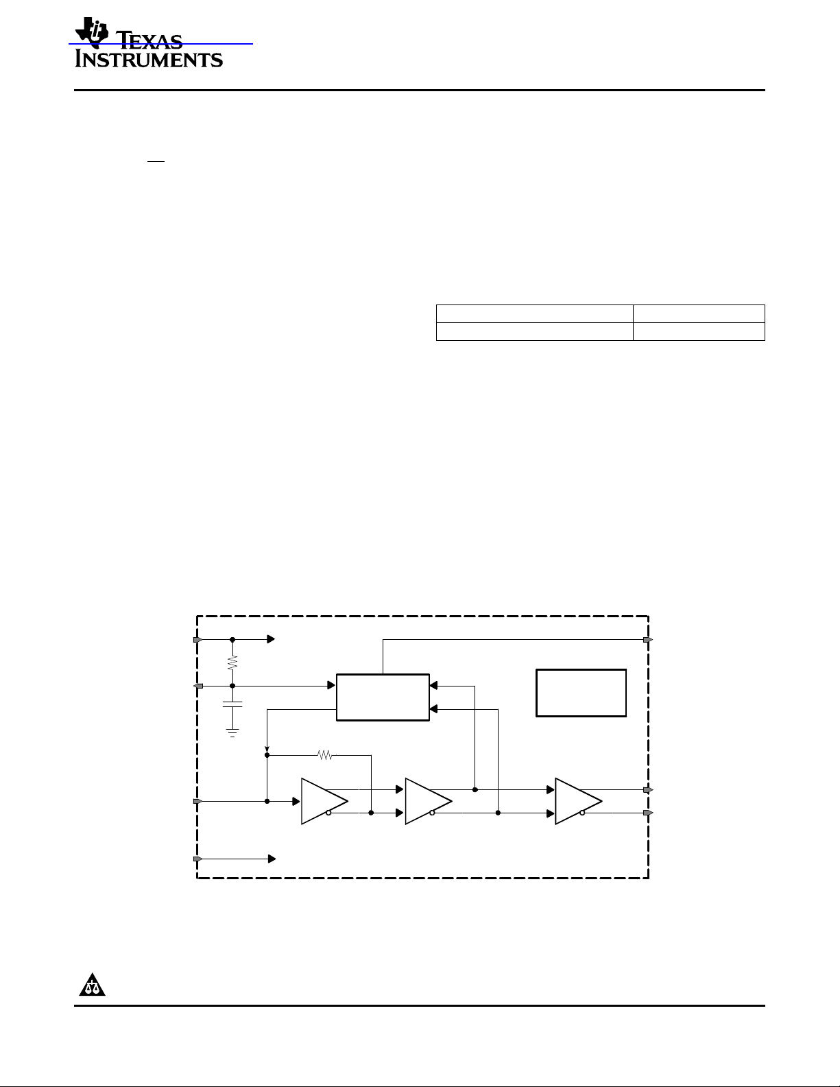
BLOCKDIAGRAM
The ONET2511TA is a high performance 2.5 Gbps transimpedance amplifier that can be segmented into the
signal path, filter, and offset cancellation block.
The signal path consists of a transimpedance amplifier stage, a voltage amplifier, and an output buffer.
The filter circuit provides a filtered VCC for the photodiode.
The offset correction circuit uses an internal low pass filter to cancel the DC on the input and it provides a signal
to monitor the received signal strength.
A simplified block diagram of the ONET2511TA is shown in Figure 1 .
Figure 1. Simplified Block Diagram of the ONET2511TA
Please be aware that an important notice concerning availability, standard warranty, and use in critical applications of Texas
Instruments semiconductor products and disclaimers thereto appears at the end of this data sheet.
PRODUCTION DATA information is current as of publication date.
Products conform to specifications per the terms of the Texas
Instruments standard warranty. Production processing does not
necessarily include testing of all parameters.
Copyright © 2004, Texas Instruments Incorporated
www.ti.com
1,030µm
654µm
origin
0,0
x
y
PAD#1
ONET2511TA_B2003
1
2 3
4
5
67
8
9
10
ONET
2511TA
2 3
4
5
6
1
VCC
N.C.
FILTER
IN109
8
7
OUT+
OUT–
GND
RSSI
GND
VCC
ONET2511TA
2.5 GBPS TRANSIMPEDANCE AMPLIFIER WITH RSSI
SLLS622 – SEPTEMBER 2004
DETAILED DESCRIPTION (continued)
SIGNAL PATH
The first stage of the signal path is a transimpedance amplifier that takes the photodiode current and converts it
to a voltage signal. The second stage is a voltage amplifier that provides additional gain. The output of the
second stage feeds the output buffer and the offset cancellation circuitry. The third and final signal path stage of
the ONET2511TA is the output buffer. The output buffer provides CML outputs with an on-chip 50 Ω
back-termination to VCC.
FILTER CIRCUITRY
The filter pin provides a filtered VCC for the photodiode bias. The on-chip low pass filter for the photodiode VCC
is implemented using a filter resistor of 750 Ω and an internal capacitor. If additional filtering is required for the
application, an external capacitor should be connected to the FILTER pin.
OFFSET CANCELLATION AND RSSI
The offset cancellation circuitry performs low pass filtering of the output signal of the voltage amplifier. This
senses the DC offset at the input of the ONET2511TA. The circuitry subtracts current from the input to effectively
cancel the DC. The sensed current is mirrored and is used to generate the RSSI output through an external 10
k Ω resistor. To disable the offset correction loop, the FILTER pin should be tied to GND.
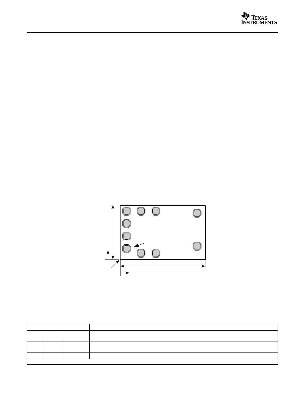
BOND PAD DESCRIPTION
The ONET2511TA is available as bare-die. The location of the bondpads is shown in Figure 2 . The circuit is
characterized for ambient temperatures between –40 ° C and 85 ° C. Table 1 shows the pad descriptions for the
ONET2511TA.
PAD SYMBOL TYPE DESCRIPTION
1 FILTER Analog Bias voltage for photodiode (connects to an internal 750- Ω resistor to VCC). To disable offset correction
2 RSSI Analog-Out Analog output voltage proportional to the input data amplitude. Indicates the strength of the received
3, 6 GND Supply Circuit ground.
2
Figure 2. Bond Pad Assignment of ONET2511TA
Table 1. Pad Description of the ONET2511TA
loop connect FILTER to GND.
signal (RSSI).
www.ti.com
ONET2511TA
2.5 GBPS TRANSIMPEDANCE AMPLIFIER WITH RSSI
SLLS622 – SEPTEMBER 2004
DETAILED DESCRIPTION (continued)
Table 1. Pad Description of the ONET2511TA (continued)
PAD SYMBOL TYPE DESCRIPTION
4 OUT- Analog-Out Inverted data output. On-chip 50- Ω back-terminated to VCC.
5 OUT+ Analog-Out Non-inverted data output. On-chip 50- Ω back-terminated to VCC.
7, 8 VCC Supply 3.3-V ± 10% supply voltage
9 IN Analog-In Data input to TIA. Connect to anode of PIN or APD diode.
10 NC Not connected
ABSOLUTE MAXIMUM RATINGS
over operating free-air temperature range (unless otherwise noted)
V
CC
V
V
OUT+
V
FILTER
I
IN
I
FILTER
Supply voltage
Voltage of OUT+ and Out-
OUT-
V
Voltage of FILTER and RSSI
RSSI
Current into IN -4 to 4 mA
Current into FILTER -8 to 8 mA
ESD ESD rating at all pins except IN
ESD rating at IN
T
Jmax
T
STG
T
A
Maximum junction temperature 150 ° C
Storage temperature -65 to 85 ° C
Operating free-air tempature -40 to 85 ° C
(1) Stresses beyond those listed under "absolute maximum ratings" may cause permanent damage to the device. These are stress ratings
only, and functional operation of the device at these or any other conditions beyond those indicated under "recommended operating
conditions" is not implied. Exposure to absolute–maximum–rated conditions for extended periods may affect device reliability.
(2) All voltage values are with respect to network ground terminal.
(3) For optimum high-frequency performance, the input pin has reduced ESD protection.
(2)
(2)
(2)
(3)
(3)
(1)
-0.3 to 4.0 V
VCC– 1.5 to V
+0.5 V
CC
-0.3 to 4.0 V
2 kV (HBM)
1 kV (HBM)
UNIT
RECOMMENDED OPERATING CONDITIONS
over operating free-air temperature range (unless otherwise noted)
PARAMETER TEST CONDITIONS MIN NOM MAX UNIT
V
CC
T
A
Supply voltage 3 3.3 3.6 V
Operating free-air temperature -40 85 ° C
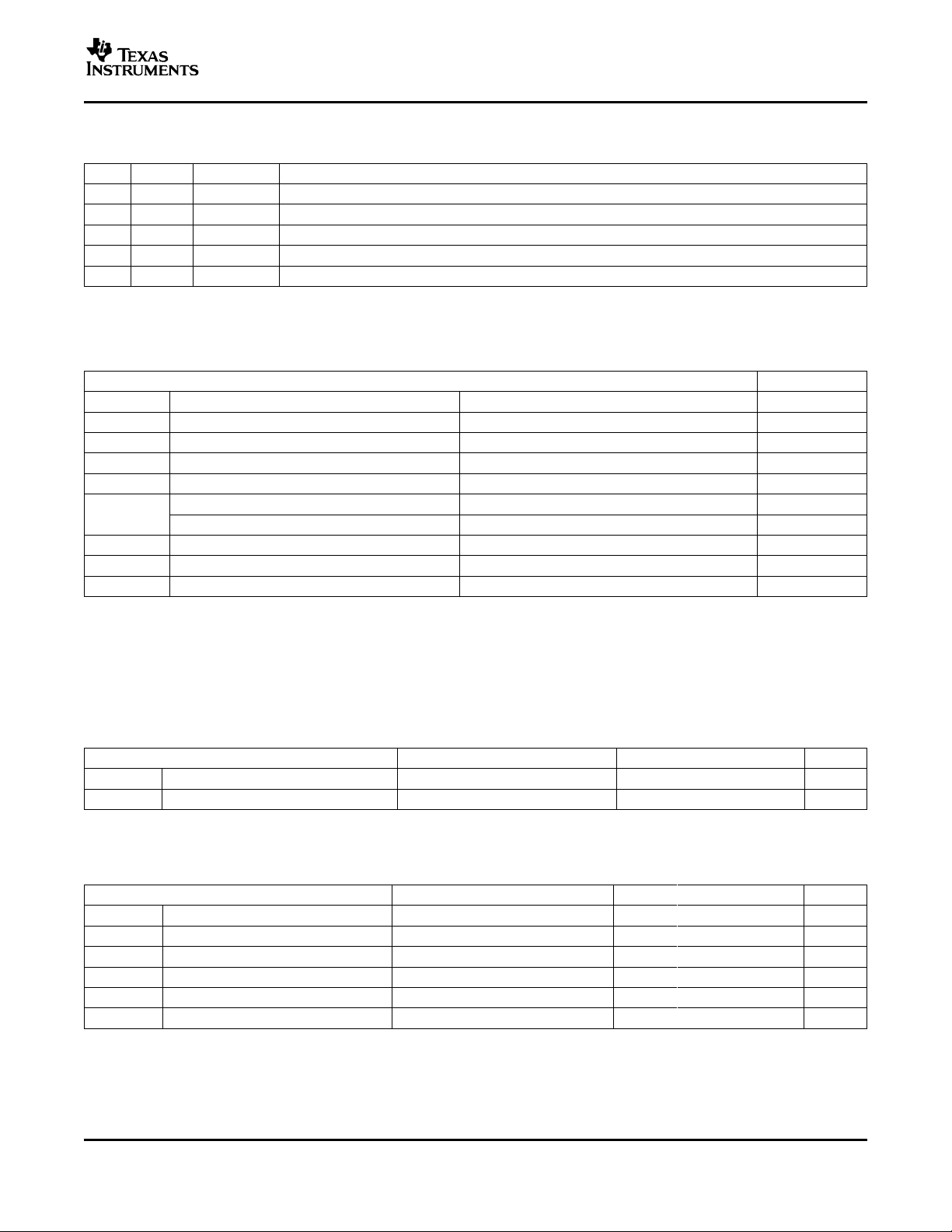
DC ELECTRICAL CHARACTERISTICS
over operating free-air temperature range, V
PARAMETER TEST CONDITIONS MIN TYP MAX UNIT
V
CC
I
CC
V
IB
I
IN-OVL
R
OUT
R
FILTER
Supply voltage 3 3.3 3.6 V
Supply current 25 35 mA
Input bias voltage 0.66 0.83 1.1 V
DC input overload current 2 mA
Ouput resistance (OUT+, OUT-) Single-ended to V
Photodiode filter resistance (FILTER) 750 Ω
= 3.3 V, TA= 25 ° C (unless otherwise noted)
CC
CC
50 Ω
3

www.ti.com
ONET2511TA
2.5 GBPS TRANSIMPEDANCE AMPLIFIER WITH RSSI
SLLS622 – SEPTEMBER 2004
AC ELECTRICAL CHARACTERISTICS
over operating free-air temperature range, V
PARAMETER TEST CONDITIONS MIN TYP MAX UNIT
I
IN-OVL
A
RSSI
Z
21
f
H-3dB
f
L-3dB
f
H-3dB-RSSI
I
N-IN
DJ Deterministic jitter IIN= 10 µA (K28.5 pattern) 21 ps
V
OD(MAX)
PSRR Power supply rejection ratio f < 2 MHz 55 dB
AC input overload current 2 mA
Input linear range 0.95 < linearity < 1.05 40 µA
RSSI gain 10-k Ω load 2000 V/A
Small-signal transimpedance Differential output 3000 4000 5000 Ω
Small-signal bandwidth C
Low-frequency -3dB bandwidth -3 dB, IIN< 20 µA DC 7 kHz
RSSI bandwidth 4 kHz
Input refered RMS noise 470 640 nA
Input refered noise density 10 pA/ √ Hz
Differential output voltage, maximum IIN= 1 mA
= 3.3 V, TA= 25 ° C (unless otherwise noted)
CC
EXTERNAL
= 0.85 pF
(1)
2.5 GHz
IIN= 100 µA (K28.5 pattern) 25 ps
IIN= 2 mA (K28.5 pattern) 16 ps
p-p
200 320 400 mV
p-p
p-p
RMS
p-p
p-p
p-p
p-p
(1) C
EXTERNAL
bondpad.
= is the total capacitance comprising of the photodiode capacitance, board capacitance, and pad capacitance at the IN
4

www.ti.com
PAD#1
ONET2511TA_B2003
1
2 3
4
5
67
8
9
10
ONET
2511TA
VCC
GND
OUT–
OUT+
RSSI
10k
750Ω
C
FILTER
(optional)
C
1
C
2
ONET2511TA
2.5 GBPS TRANSIMPEDANCE AMPLIFIER WITH RSSI
SLLS622 – SEPTEMBER 2004
APPLICATION INFORMATION
Basic Application Circuit
Figure 3 shows the ONET2511TA being used as a receiver in a typical fiber optic application. The ONET2511TA
converts the electrical current generated by the PIN or APD photodiode into a differential voltage output. The
FILTER input provides a DC bias voltage for the photodiode that is low pass filtered by the combination of the
internal 750- Ω resistor and internal capacitor. For additional power supply filtering, use an external capacitor
C
resistor to GND or left open. Within the ONET2511TA, the OUT+ and OUT- pins are back-terminated with 50 Ω
to VCC.
. The RSSI output is used to mirror the photodiode output current and must be connected via a 10-k Ω
FILTER
Figure 3. Basic Application Circuit
Board Layout
Careful attention to board layout parasitics and external components is necessary to achieve optimal
performance with a high performance transimpedance amplifier like the ONET2511TA.
Recommendations that optimize performance include:
1. Minimize total capacitance on the IN pad by using a low capacitance photodiode and paying attention to
stray capacitances. Place the photodiode close to the ONET2511TA die in order to minimize the bond wire
length and thus the parasitic inductance.
2. The external filter capacitance C
chosen with care based on the module implementation.
3. Use identical termination and symmetrical transmission lines at the differential output pins OUT+ and OUT-.
4. Use short bond wire connections for the supply terminals VCC and GND. Provide sufficient supply voltage
filtering.
may have an impact on the transfer function of the TIA and must be
FILTER
5
www.ti.com
1,030µm
654µm
origin
0,0
x
y
PAD#1
ONET2511TA_B2003
1
2 3
4
5
67
8
9
10
ONET
2511TA
ONET2511TA
2.5 GBPS TRANSIMPEDANCE AMPLIFIER WITH RSSI
SLLS622 – SEPTEMBER 2004
APPLICATION INFORMATION (continued)
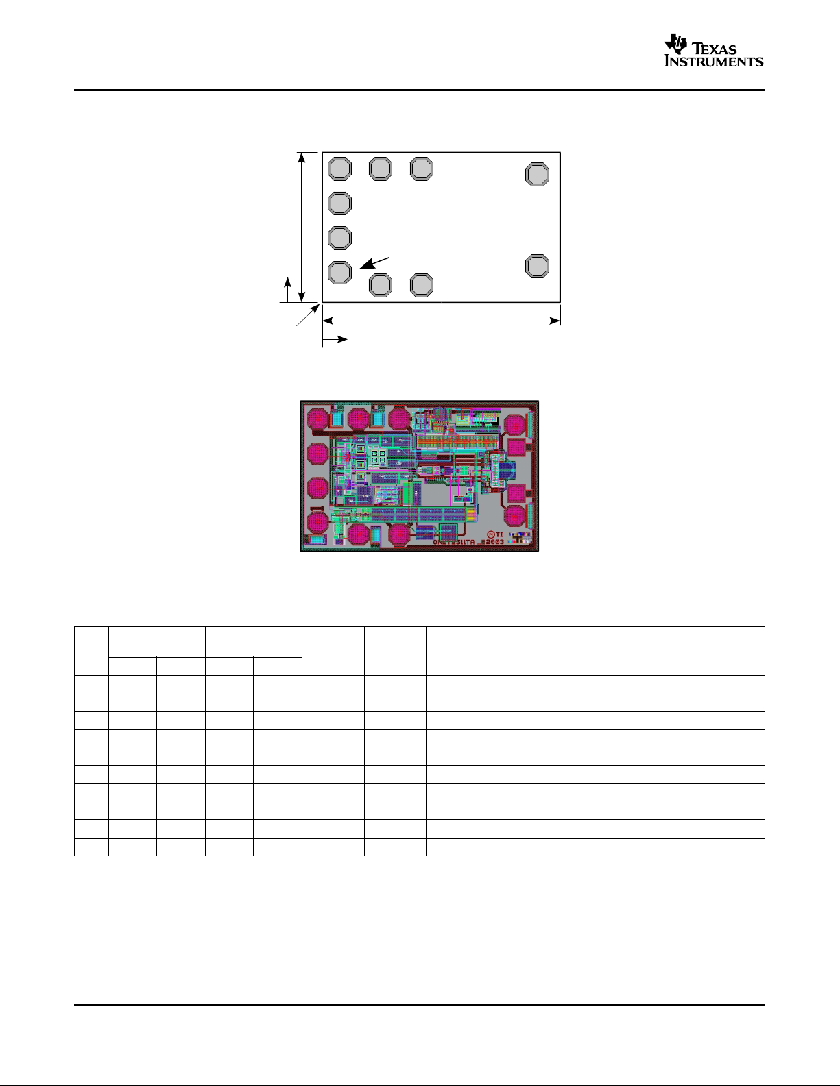
CHIP DIMENSIONS AND PAD LOCATIONS
Figure 4. Chip Dimensions and Pad Locations
Figure 5. Chip Layout
Pad Locations and Description
PAD LOWER LEFT UPPER RIGHT SYMBOL TYPE DESCRIPTION
COORDINATE COORDINATE
x [µm] y [µm] x [µm] y [µm]
1 30 84 115 169 FILTER Analog Bias voltage for photodiode
2 207 30 292 115 RSSI Analog out RSSI output voltage signal
3 384 30 469 115 GND Supply Circuit ground
4 886 112 971 197 OUT- Analog out Inverted data output
5 886 509 971 594 OUT+ Analog out Non-inverted data output
6 384 534 469 619 GND Supply Circuit ground
7 207 534 292 619 VCC Supply +3.3 V ± 10% supply voltage
8 30 534 115 619 VCC Supply +3.3 V ± 10% supply voltage
9 30 384 115 469 IN Analog in Data input to TIA
10 30 234 115 319 NC Not connected
6
www.ti.com
PAD#1
ONET2511TA_B2003
1
2 3
4
5
67
8
9
10
ONET
2511TA
1.03mm
0.65mm
OUT+ OUT–
VCC RSSI
GND
2.5 GBPS TRANSIMPEDANCE AMPLIFIER WITH RSSI
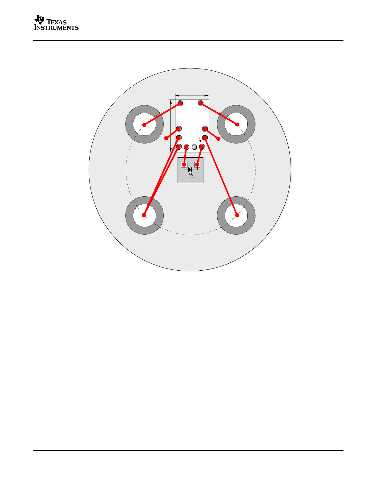
TO46 Layout Example
An example for a suggested layout in a 5-pin TO46 ROSA is given in Figure 6 (top view).
ONET2511TA
SLLS622 – SEPTEMBER 2004
Figure 6. TO46 Layout Example Using the ONET2511TA
7

www.ti.com
500
400
350
250
−40 −20 100
Free−Air Tempature − C
Input Reffered Noise Current − nA
600
200
300
450
550
0 20 40 60 80
RMS
1600
1200
1000
600
1 10 100 1000
Average Input Current − A
2000
400
800
1400
1800
2400
2200
Input Reffered Noise Current − nA
RMS
100
0
−50
−150
−100 −80 −40 −20 0
Input Current − A
Differential Output Voltage − mV
200
−200
−100
50
150
−60 100804020 60
71
69
68
66
−40 −20 100
Free−Air Tempature − C
73
65
67
70
72
0 20 40 60 80
Transimpedance − dB
75
74
ONET2511TA
2.5 GBPS TRANSIMPEDANCE AMPLIFIER WITH RSSI
SLLS622 – SEPTEMBER 2004
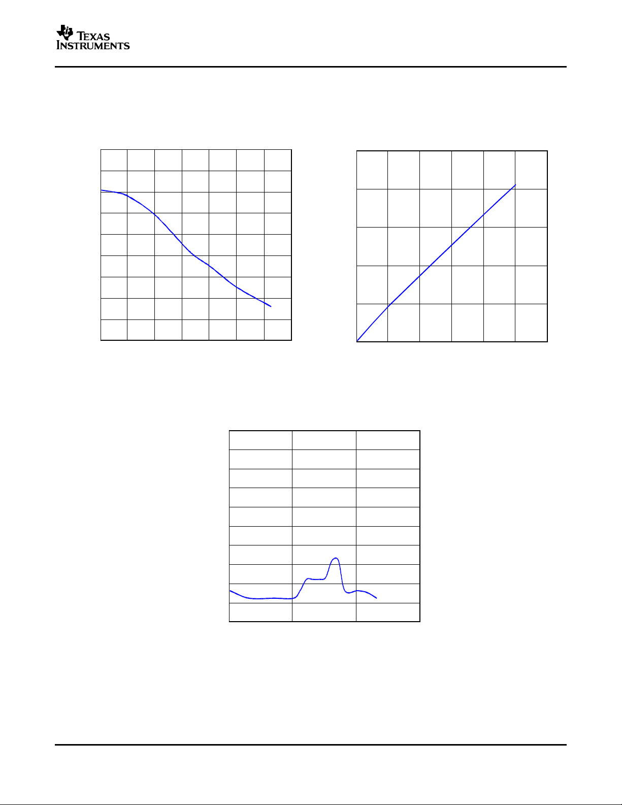
TYPICAL CHARACTERISTICS
V
= +3.3 V and TA= +25 ° C (unless otherwise noted)
CC
INPUT REFERRED NOISE INPUT REFERRED NOISE
AVERAGE INPUT CURRENT FREE-AIR TEMPERATURE
DC TRANSFER CHARACTERISTIC (OFFSET CANCEL- vs
LATION DISABLED) FREE-AIR TEMPERATURE
vs vs
Figure 7. Figure 8.
TRANSIMPEDANCE
8
Figure 9. Figure 10.
www.ti.com
2.7
2.5
2.4
2.2
−40 −20 100
Free−Air Tempature − C
2.9
2.1
2.3
2.6
2.8
0 20 40 60 80
Small−Signal Bandwdith − GHz
3.0
2
1.5
0.5
0 200 600 800 1200
Average Input Current − A
RSSI Output Voltage − V
0
1
2.5
400 1000
60
40
30
10
10 100 10k
Input Current − A
p−p
80
0
20
50
70
100
90
1000
Deterministic Jitter − ps
p−p
TYPICAL CHARACTERISTICS (continued)
V
= +3.3 V and TA= +25 ° C (unless otherwise noted)
CC
ONET2511TA
2.5 GBPS TRANSIMPEDANCE AMPLIFIER WITH RSSI
SLLS622 – SEPTEMBER 2004
SMALL SIGNAL BANDWIDTH RSSI OUTPUT VOLTAGE
FREE-AIR TEMPERATURE AVERAGE INPUT CURRENT
vs vs
Figure 11. Figure 12.
DETERMINISTIC JITTER
vs
INPUT CURRENT
Figure 13.
9

www.ti.com
Time − 100ps/Div
Differential Output Voltage − 15mV/Div
Time − 100ps/Div
Differential Output Voltage − 50mV/Div
ONET2511TA
2.5 GBPS TRANSIMPEDANCE AMPLIFIER WITH RSSI
SLLS622 – SEPTEMBER 2004
TYPICAL CHARACTERISTICS (continued)
V
= +3.3 V and TA= +25 ° C (unless otherwise noted)
CC
OUTPUT EYE-DIAGRAM AT 2.5 GBPS and 20µA
INPUT CURRENT USING A K28.5 PATTERN
p-p
OUTPUT EYE-DIAGRAM AT 2.5 GBPS and 2 mA
Figure 14.
INPUT CURRENT USING A K28.5 PATTERN
p-p
Figure 15.
10

PACKAGE OPTION ADDENDUM
www.ti.com
12-Jan-2006
PACKAGING INFORMATION
Orderable Device Status
(1)
Package
Type
Package
Drawing
Pins Package
Qty
Eco Plan
ONET2511TAY ACTIVE XCEPT Y 10 418 Green (RoHS &
no Sb/Br)
(1)
The marketing status values are defined as follows:
ACTIVE: Product device recommended for new designs.
LIFEBUY: TI has announced that the device will be discontinued, and a lifetime-buy period is in effect.
NRND: Not recommended for new designs. Device is in production to support existing customers, but TI does not recommend using this part in
a new design.
PREVIEW: Device has been announced but is not in production. Samples may or may not be available.
OBSOLETE: TI has discontinued the production of the device.
(2)
Eco Plan - The planned eco-friendly classification: Pb-Free (RoHS), Pb-Free (RoHS Exempt), or Green (RoHS & no Sb/Br) - please check
http://www.ti.com/productcontent for the latest availability information and additional product content details.
TBD: The Pb-Free/Green conversion plan has not been defined.
Pb-Free (RoHS): TI's terms "Lead-Free" or "Pb-Free" mean semiconductor products that are compatible with the current RoHS requirements
for all 6 substances, including the requirement that lead not exceed 0.1% by weight in homogeneous materials. Where designed to be soldered
at high temperatures, TI Pb-Free products are suitable for use in specified lead-free processes.
Pb-Free (RoHS Exempt): This component has a RoHS exemption for either 1) lead-based flip-chip solder bumps used between the die and
package, or 2) lead-based die adhesive used between the die and leadframe. The component is otherwise considered Pb-Free (RoHS
compatible) as defined above.
Green (RoHS & no Sb/Br): TI defines "Green" to mean Pb-Free (RoHS compatible), and free of Bromine (Br) and Antimony (Sb) based flame
retardants (Br or Sb do not exceed 0.1% by weight in homogeneous material)
(2)
Lead/Ball Finish MSL Peak Temp
Call TI N / A for Pkg Type
(3)
(3)
MSL, Peak Temp. -- The Moisture Sensitivity Level rating according to the JEDEC industry standard classifications, and peak solder
temperature.
Important Information and Disclaimer:The information provided on this page represents TI's knowledge and belief as of the date that it is
provided. TI bases its knowledge and belief on information provided by third parties, and makes no representation or warranty as to the
accuracy of such information. Efforts are underway to better integrate information from third parties. TI has taken and continues to take
reasonable steps to provide representative and accurate information but may not have conducted destructive testing or chemical analysis on
incoming materials and chemicals. TI and TI suppliers consider certain information to be proprietary, and thus CAS numbers and other limited
information may not be available for release.
In no event shall TI's liability arising out of such information exceed the total purchase price of the TI part(s) at issue in this document sold by TI
to Customer on an annual basis.
Addendum-Page 1

IMPORTANT NOTICE
Texas Instruments Incorporated and its subsidiaries (TI) reserve the right to make corrections, modifications,
enhancements, improvements, and other changes to its products and services at any time and to discontinue
any product or service without notice. Customers should obtain the latest relevant information before placing
orders and should verify that such information is current and complete. All products are sold subject to TI’s terms
and conditions of sale supplied at the time of order acknowledgment.
TI warrants performance of its hardware products to the specifications applicable at the time of sale in
accordance with TI’s standard warranty. Testing and other quality control techniques are used to the extent TI
deems necessary to support this warranty. Except where mandated by government requirements, testing of all
parameters of each product is not necessarily performed.
TI assumes no liability for applications assistance or customer product design. Customers are responsible for
their products and applications using TI components. To minimize the risks associated with customer products
and applications, customers should provide adequate design and operating safeguards.
TI does not warrant or represent that any license, either express or implied, is granted under any TI patent right,
copyright, mask work right, or other TI intellectual property right relating to any combination, machine, or process
in which TI products or services are used. Information published by TI regarding third-party products or services
does not constitute a license from TI to use such products or services or a warranty or endorsement thereof.
Use of such information may require a license from a third party under the patents or other intellectual property
of the third party, or a license from TI under the patents or other intellectual property of TI.
Reproduction of information in TI data books or data sheets is permissible only if reproduction is without
alteration and is accompanied by all associated warranties, conditions, limitations, and notices. Reproduction
of this information with alteration is an unfair and deceptive business practice. TI is not responsible or liable for
such altered documentation.
Resale of TI products or services with statements different from or beyond the parameters stated by TI for that
product or service voids all express and any implied warranties for the associated TI product or service and
is an unfair and deceptive business practice. TI is not responsible or liable for any such statements.
Following are URLs where you can obtain information on other Texas Instruments products and application
solutions:
Products Applications
Amplifiers amplifier.ti.com Audio www.ti.com/audio
Data Converters dataconverter.ti.com Automotive www.ti.com/automotive
DSP dsp.ti.com Broadband www.ti.com/broadband
Interface interface.ti.com Digital Control www.ti.com/digitalcontrol
Logic logic.ti.com Military www.ti.com/military
Power Mgmt power.ti.com Optical Networking www.ti.com/opticalnetwork
Microcontrollers microcontroller.ti.com Security www.ti.com/security
Telephony www.ti.com/telephony
Video & Imaging www.ti.com/video
Wireless www.ti.com/wireless
Mailing Address: Texas Instruments
Post Office Box 655303 Dallas, Texas 75265
Copyright 2006, Texas Instruments Incorporated
 Loading...