Product
Folder
Order
Now
Technical
Documents
Tools &
Software
Support &
Community
DLPS013G –APRIL 2010–REVISED JANUARY 2019
DLP5500 DLP®0.55 XGA Series 450 DMD
DLP5500
1 Features
1
• 0.55-Inch Micromirror Array Diagonal
– 1024 × 768 Array of Aluminum, Micrometer-
Sized Mirrors (XGA Resolution)
– 10.8-µm Micromirror Pitch
– ±12° Micromirror Tilt Angle
(Relative to Flat State)
– Designed for Corner Illumination
• Designed for Use With Broadband Visible Light
(420 nm – 700 nm):
– Window Transmission 97% (Single Pass,
Through Two Window Surfaces)
– Micromirror Reflectivity 88%
– Array Diffraction Efficiency 86%
– Array Fill Factor 92%
• 16-Bit, Low Voltage Differential Signaling (LVDS)
Double Data Rate (DDR) Input Data Bus
• 200 MHz Input Data Clock Rate
• Dedicated DLPC200 Controller for High-Speed
Pattern Rates:
– 5,000 Hz (1-Bit Binary Patterns)
– 500 Hz (8-Bit Grayscale Patterns)
• Series 450 Package Characteristics:
– Thermal Area 18 mm × 12 mm Enabling High
on Screen Lumens (>2000 lm)
– 149 Micro Pin Grid Array Robust Electrical
Connection
– Package Mates to Amphenol InterCon
Systems 450-2.700-L-13.25-149 Socket
2 Applications
• Industrial
– 3D Scanners for Machine Vision and Quality
Control
– 3D Printing
– Direct Imaging Lithography
– Laser Marking and Repair
– Industrial and Medical Imaging
– Medical Instrumentation
– Digital Exposure Systems
• Medical
– Opthamology
– 3D Scanners for Limb and Skin Measurement
– Hyperspectral Imaging
• Displays
– 3D Imaging Microscopes
– Intelligent and Adaptive Lighting
3 Description
Featuring over 750000 micromirrors, the high
resolution DLP5500 (0.55" XGA) digital micromirror
device (DMD) is a spatial light modulator (SLM) that
modulates the amplitude, direction, and/or phase of
incoming light. This advanced light control technology
has numerous applications in the industrial, medical,
and consumer markets. The DLP5500 enables fine
resolution for 3D printing applications.
Device Information
PART NUMBER PACKAGE BODY SIZE (NOM)
DLP5500 CPGA (149) 22.30 mm × 32.20 mm
(1) For all available packages, see the orderable addendum at
the end of the data sheet.
(1)
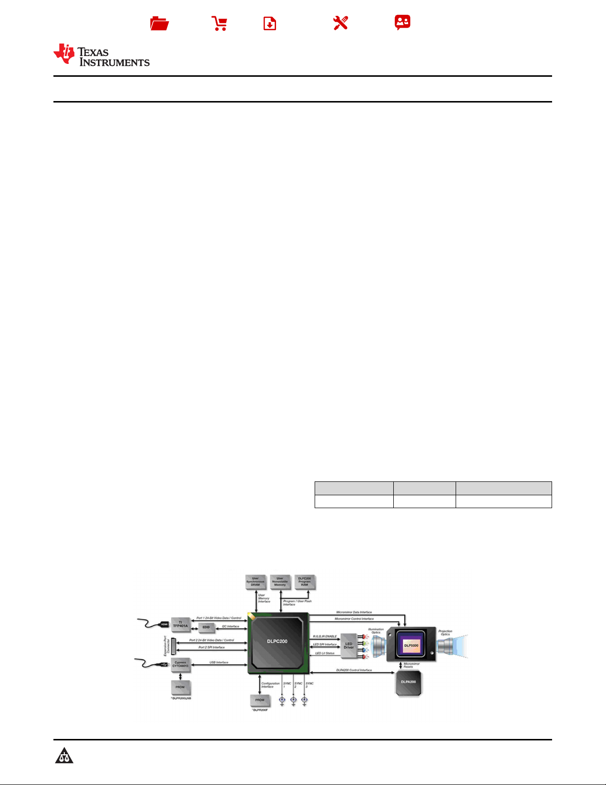
4 Typical Application Schematic
1
An IMPORTANT NOTICE at the end of this data sheet addresses availability, warranty, changes, use in safety-critical applications,
intellectual property matters and other important disclaimers. PRODUCTION DATA.

DLP5500
DLPS013G –APRIL 2010–REVISED JANUARY 2019
www.ti.com
Table of Contents
1 Features.................................................................. 1
2 Applications ........................................................... 1
3 Description ............................................................. 1
4 Typical Application Schematic............................. 1
5 Revision History..................................................... 2
6 Description (continued)......................................... 4
7 Pin Configuration and Functions......................... 4
8 Specifications......................................................... 7
8.1 Absolute Maximum Ratings...................................... 7
8.2 Storage Conditions.................................................... 7
8.3 ESD Ratings.............................................................. 7
8.4 Recommended Operating Conditions....................... 8
8.5 Thermal Information................................................ 10
8.6 Electrical Characteristics......................................... 10
8.7 Timing Requirements.............................................. 11
8.8 System Mounting Interface Loads .......................... 15
8.9 Micromirror Array Physical Characteristics............. 16
8.10 Micromirror Array Optical Characteristics............. 17
8.11 Window Characteristics......................................... 18
8.12 Chipset Component Usage Specification ............. 18
9 Detailed Description............................................ 19
9.1 Overview................................................................. 19
9.2 Functional Block Diagram....................................... 20
9.3 Feature Description................................................. 21
9.4 Device Functional Modes........................................ 24
9.5 Window Characteristics and Optics ....................... 24
9.6 Micromirror Array Temperature Calculation............ 25
9.7 Micromirror Landed-on/Landed-Off Duty Cycle...... 27
10 Application and Implementation........................ 29
10.1 Application Information.......................................... 29
10.2 Typical Application................................................ 30
11 Power Supply Recommendations ..................... 32
11.1 DMD Power-Up and Power-Down Procedures..... 32
12 Layout................................................................... 32
12.1 Layout Guidelines ................................................. 32
12.2 Layout Example .................................................... 33
13 Device and Documentation Support................. 34
13.1 Device Support .................................................... 34
13.2 Documentation Support ........................................ 34
13.3 Related Documentation......................................... 34
13.4 Community Resources.......................................... 34
13.5 Trademarks........................................................... 35
13.6 Electrostatic Discharge Caution............................ 35
13.7 Glossary................................................................ 35
14 Mechanical, Packaging, and Orderable
Information........................................................... 35
5 Revision History
Changes from Revision F (May 2015) to Revision G Page
• Changed DMD Marking Image Object for Figure 19 ........................................................................................................... 34
Changes from Revision E (September 2013) to Revision F Page
• Added ESD Ratings, Feature Description section, Device Functional Modes, Application and Implementation
section, Power Supply Recommendations section, Layout section, Device and Documentation Support section, and
Mechanical, Packaging, and Orderable Information section ................................................................................................. 1
• Changed Incorrect V
• Changed LVDS ƒ
• Added Max Recommended DMD Temperature – Derating Curve......................................................................................... 9
• Added LVCMOS Output Measurement Condition Figure..................................................................................................... 10
• Changed Incorrect tCvalue from 4 ns to 5 ns (200 MHz clock) ........................................................................................... 11
• Changed Incorrect tWvalue from 1.25 ns to 2.5 ns (200 MHz clock)................................................................................... 11
• Changed SCP Bus Diagrams............................................................................................................................................... 11
• Added LVDS Voltage Definition Figure ................................................................................................................................ 12
• Changed LVDS Waveform Requirements Figure................................................................................................................. 13
• Added LVDS Equivalent Input Circuit Figure ....................................................................................................................... 13
• Added LVDS & SCP Rise and Fall Time Figures................................................................................................................. 14
• Moved the Mechanical section from Recommended Operating Conditions table to the System Mounting Interface
Loads section ...................................................................................................................................................................... 15
• Added Micromirror Array Physical Characteristics section .................................................................................................. 16
• Changed Micromirror Array Physical Characteristics Figure to generic image (M x N)....................................................... 16
value from 9V to 8V......................................................................................................................... 7
CC2
to200 MHz - previously incorrectly listed as 150 MHz......................................................................... 9
clock
2
Submit Documentation Feedback Copyright © 2010–2019, Texas Instruments Incorporated
Product Folder Links: DLP5500

DLP5500
www.ti.com
• Added Micromirror Array Optical Characteristics section .................................................................................................... 17
• Changed specular reflectivity wavelength range to 420 - 700 nm (from 400 - 700 nm) to match Recommended
Operating Conditions............................................................................................................................................................ 17
• Changed Micromirror Landed Orientation and Tilt Figure to generic image (M x N) ........................................................... 18
• Added Window Characteristics section ............................................................................................................................... 18
• Added Chipset Component Usage Specification section .................................................................................................... 18
• Changed Micromirror Array, Pitch, Hinge Axis Orientation Figure to generic image (M x N).............................................. 22
• Changed Micromirror States: On, Off, Flat Figure to generic DMD image .......................................................................... 23
• Changed Test Point locations from TC1 & TC2 to TP1 - TP5 ............................................................................................. 25
• Changed Test Point location Diagram to show TP1 - TP5................................................................................................... 26
• Added Micromirror Landed-on/Landed-Off Duty Cycle section............................................................................................ 27
• Changed Typical Application diagram.................................................................................................................................. 30
• Replaced "DAD" with "DLPA200"......................................................................................................................................... 31
Changes from Revision D (October 2012) to Revision E Page
• Deleted the Device Part Number Nomenclature section...................................................................................................... 34
Changes from Revision C (June 2012) to Revision D Page
DLPS013G –APRIL 2010–REVISED JANUARY 2019
• Changed the Device Part Number Nomenclature From: DLP5500FYA To: DLP5500AFYA............................................... 34
• Updated Mechanical ICD to V2 with a minor change in the window height......................................................................... 34
Changes from Revision B (Spetember 2011) to Revision C Page
• Added the Package Footprint and Socket information in the Features list ........................................................................... 1
• Deleted redundant information from the Description.............................................................................................................. 1
• Changed the Illumination power density Max value of <420 mm From: 20 To: 2 mW/cm2................................................... 7
• Changed Storage temperature range and humidity values in Absolute Maximum Ratings .................................................. 7
• Added Operating Case Temperature, Operating Humidity, Operating Device Temperature Gradient and Operating
Landed Duty-Cycle to RECOMMENDED OPERATING CONDITIONS................................................................................. 8
• Added Mirror metal specular reflectivity and Illumination overfill values to "Micromirror Array Optical Characteristics"
table...................................................................................................................................................................................... 17
• Corrected the C
, Qarray and T
L2W
values in Micromirror Array Temperature Calculation for Uniform Illumination. ...... 26
array
• Corrected the document reference in Related Documents section...................................................................................... 34
Changes from Revision A (June 2010) to Revision B Page
• Changed the window refractive index NOM spec From: 1.5090 To: 1.5119 ....................................................................... 17
• Added table note "At a wavelength of 632.8 nm"................................................................................................................. 17
Changes from Original (April 2010) to Revision A Page
• Changed V
REF
to V
............................................................................................................................................................. 7
CC1
• Added |VID| to the absolute max table.................................................................................................................................... 7
• Added V
to the absolute max table................................................................................................................................ 7
MBRST
• Clarified Note6 measurement point ....................................................................................................................................... 7
• Changed the Illumination power density Max value of <420 mm From: 2 To: 20 mW/cm2................................................... 7
• Added Additional Related Documents.................................................................................................................................. 34
Submit Documentation FeedbackCopyright © 2010–2019, Texas Instruments Incorporated
Product Folder Links: DLP5500
3
DLP5500
DLPS013G –APRIL 2010–REVISED JANUARY 2019
www.ti.com
6 Description (continued)
The XGA resolution has the direct benefit of scanning large objects for 3D machine vision applications. Reliable
function and operation of the DLP5500 requires that it be used in conjunction with the DLPC200 digital controller
and the DLPA200 analog driver. This dedicated chipset provides a robust, high resolution XGA, and high speed
system solution.
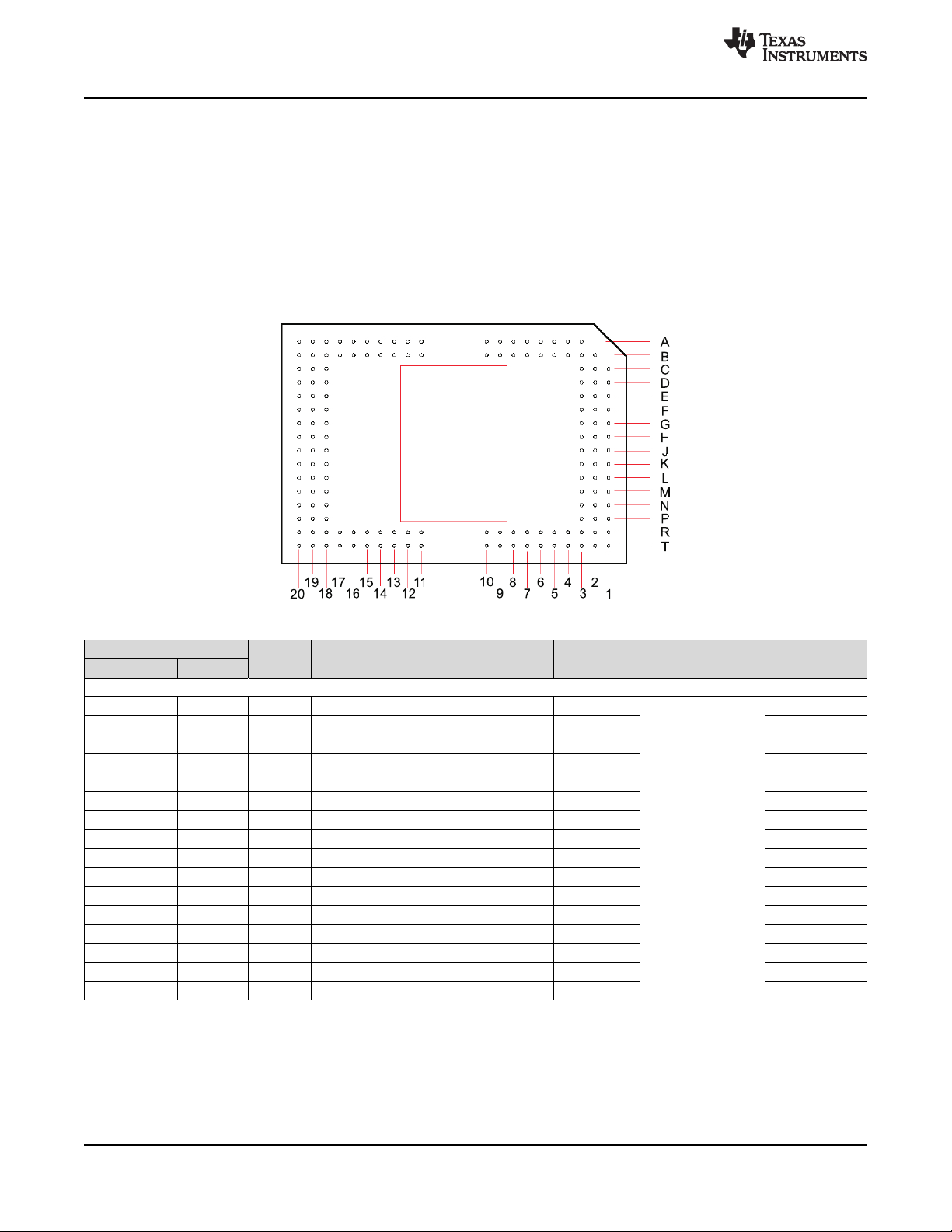
7 Pin Configuration and Functions
FYA Package
149-Pin CPGA Series 450
Bottom View
(1)
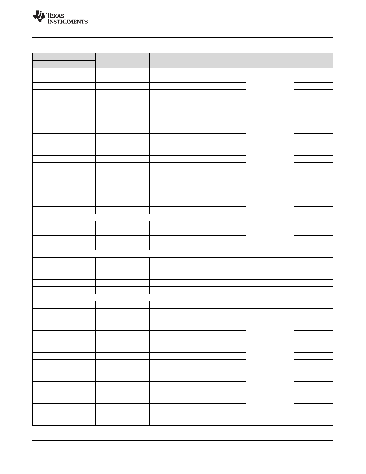
Pin Functions
PIN
NAME NO.
DATA INPUTS
D_AN1 G20 Input LVCMOS DDR Differential DCLK_A
D_AP1 H20 Input LVCMOS DDR Differential DCLK_A 744
D_AN3 H19 Input LVCMOS DDR Differential DCLK_A 688
D_AP3 G19 Input LVCMOS DDR Differential DCLK_A 703
D_AN5 F18 Input LVCMOS DDR Differential DCLK_A 686
D_AP5 G18 Input LVCMOS DDR Differential DCLK_A 714
D_AN7 E18 Input LVCMOS DDR Differential DCLK_A 689
D_AP7 D18 Input LVCMOS DDR Differential DCLK_A 705
D_AN9 C20 Input LVCMOS DDR Differential DCLK_A 687
D_AP9 D20 Input LVCMOS DDR Differential DCLK_A 715
D_AN11 B18 Input LVCMOS DDR Differential DCLK_A 715
D_AP11 A18 Input LVCMOS DDR Differential DCLK_A 732
D_AN13 A20 Input LVCMOS DDR Differential DCLK_A 686
D_AP13 B20 Input LVCMOS DDR Differential DCLK_A 715
D_AN15 B19 Input LVCMOS DDR Differential DCLK_A 700
D_AP15 A19 Input LVCMOS DDR Differential DCLK_A 719
(1) The following power supplies are required to operate the DMD: VCC, VCCI, VCC2. VSS must also be connected.
(2) DDR = Double Data Rate. SDR = Single Data Rate. Refer to the Timing Requirements for specifications and relationships.
(3) Refer to Electrical Characteristics for differential termination specification.
(4) Internal Trace Length (mils) refers to the Package electrical trace length. See the DLP®0.55 XGA Chip-Set Data Manual (DLPZ004) for
details regarding signal integrity considerations for end-equipment designs.
4
Submit Documentation Feedback Copyright © 2010–2019, Texas Instruments Incorporated
TYPE
(I/O/P )
SIGNAL
DATA
RATE
INTERNAL
(2)
TERM
(3)
Product Folder Links: DLP5500
CLOCK DESCRIPTION
Input data bus A
(LVDS)
TRACE
(mils)
715
(4)
www.ti.com
DLPS013G –APRIL 2010–REVISED JANUARY 2019
Pin Functions (continued)
(1)
PIN
NAME NO.
D_BN1 K20 Input LVCMOS DDR Differential DCLK_B
D_BP1 J20 Input LVCMOS DDR Differential DCLK_B 745
D_BN3 J19 Input LVCMOS DDR Differential DCLK_B 686
D_BP3 K19 Input LVCMOS DDR Differential DCLK_B 703
D_BN5 L18 Input LVCMOS DDR Differential DCLK_B 686
D_BP5 K18 Input LVCMOS DDR Differential DCLK_B 714
D_BN7 M18 Input LVCMOS DDR Differential DCLK_B 693
D_BP7 N18 Input LVCMOS DDR Differential DCLK_B 709
D_BN9 P20 Input LVCMOS DDR Differential DCLK_B 687
D_BP9 N20 Input LVCMOS DDR Differential DCLK_B 715
D_BN11 R18 Input LVCMOS DDR Differential DCLK_B 702
D_BP11 T18 Input LVCMOS DDR Differential DCLK_B 719
D_BN13 T20 Input LVCMOS DDR Differential DCLK_B 686
D_BP13 R20 Input LVCMOS DDR Differential DCLK_B 715
D_BN15 R19 Input LVCMOS DDR Differential DCLK_B 680
D_BP15 T19 Input LVCMOS DDR Differential DCLK_B 700
DCLK_AN D19 Input LVCMOS - Differential –
DCLK_AP E19 Input LVCMOS - Differential – 728
DCLK_BN N19 Input LVCMOS - Differential –
DCLK_BP M19 Input LVCMOS - Differential – 728
DATA CONTROL INPUTS
SCTRL_AN F20 Input LVCMOS DDR Differential DCLK_A
SCTRL_AP E20 Input LVCMOS DDR Differential DCLK_A 731
SCTRL_BN L20 Input LVCMOS DDR Differential DCLK_B 707
SCTRL_BP M20 Input LVCMOS DDR Differential DCLK_B 722
SERIAL COMMUNICATION (SCP) AND CONFIGURATION
SCP_CLK A8 Input LVCMOS – Pull-Down – –
SCP_DO A9 Output LVCMOS – – SCP_CLK –
SCP_DI A5 Input LVCMOS – Pull-Down SCP_CLK –
SCP_EN B7 Input LVCMOS – Pull-Down SCP_CLK –
PWRDN B9 Input LVCMOS – Pull-Down – –
MICROMIRROR BIAS CLOCKING PULSE
MODE_A A4 Input LVCMOS – Pull-Down – –
MBRST0 C3 Input Analog – – –
MBRST1 D2 Input Analog – – – –
MBRST2 D3 Input Analog – – – –
MBRST3 E2 Input Analog – – – –
MBRST4 G3 Input Analog – – – –
MBRST5 E1 Input Analog – – – –
MBRST6 G2 Input Analog – – – –
MBRST7 G1 Input Analog – – – –
MBRST8 N3 Input Analog – – – –
MBRST9 M2 Input Analog – – – –
MBRST10 M3 Input Analog – – – –
MBRST11 L2 Input Analog – – – –
MBRST12 J3 Input Analog – – – –
MBRST13 L1 Input Analog – – – –
MBRST14 J2 Input Analog – – – –
MBRST15 J1 Input Analog – – – –
TYPE
(I/O/P )
SIGNAL
DATA
RATE
INTERNAL
(2)
TERM
(3)
CLOCK DESCRIPTION
Input data bus B
(LVDS)
Input data bus A Clock
(LVDS)
Input data bus B Clock
(LVDS)
Data Control (LVDS)
Micromirror Bias
Clocking Pulse
"MBRST" signals
"clock" micromirrors
into state of LVCMOS
memory cell associated
with each mirror.
DLP5500
TRACE
(4)
(mils)
716
700
700
716
–
Product Folder Links: DLP5500
Submit Documentation FeedbackCopyright © 2010–2019, Texas Instruments Incorporated
5

DLP5500
DLPS013G –APRIL 2010–REVISED JANUARY 2019
Pin Functions (continued)
(1)
PIN
NAME NO.
POWER
B11,B12,B1
V
CC
3,B16,R12,
R13,R16,R1
7
A12,A14,A1
V
CCI
V
CC2
6,T12,T14,T16Power Analog – – –
C1,D1,M1,N
1
A6,A11,A13,
A15,A17,B4,
B5,B8,B14,
B15,B17,C2
,C18,C19,F
1,F2,F19,H1
V
SS
,H2,H3,H18,
J18,K1,K2,L
19,N2,P18,
P19,R4,R9,
R14,R15,T7
,T13,T15,T1
7
RESERVED SIGNALS (Not for use in system)
RESERVED_R7 R7 Input LVCMOS – Pull-Down –
RESERVED_R8 R8 Input LVCMOS – Pull-Down – –
RESERVED_T8 T8 Input LVCMOS – Pull-Down – –
RESERVED_B6 B6 Input LVCMOS – Pull-Down – –
A3, A7,
A10, B2,
B3, B10,
E3, F3, K3,
L3, P1, P2,
NO_CONNECT
P3, R1, R2,
R3, R5, R6,
R10, R11,
T1, T2, T3,
T4, T5, T6,
T9, T10,
T11
TYPE
(I/O/P )
SIGNAL
Power Analog – – –
DATA
RATE
INTERNAL
(2)
TERM
(3)
CLOCK DESCRIPTION
Power for LVCMOS
Logic
Power supply for LVDS
Interface
Power Analog – – –
Power Analog – – –
Power for High Voltage
CMOS Logic
Common return for all
power inputs
Pins should be
connected to V
SS
– – – – – DO NOT CONNECT –
www.ti.com
TRACE
(4)
(mils)
–
–
–
–
–
6
Submit Documentation Feedback Copyright © 2010–2019, Texas Instruments Incorporated
Product Folder Links: DLP5500
DLP5500
www.ti.com
DLPS013G –APRIL 2010–REVISED JANUARY 2019
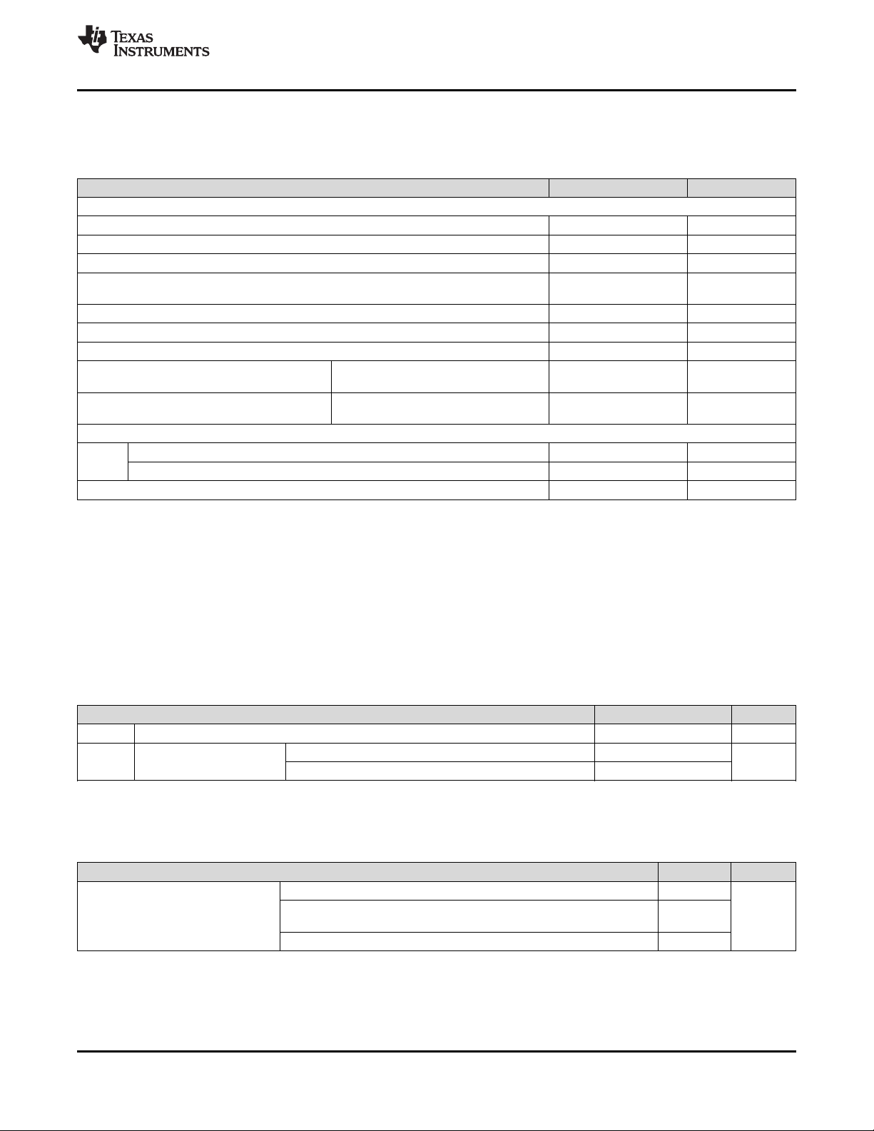
8 Specifications
8.1 Absolute Maximum Ratings
over operating free-air temperature range (unless otherwise noted)
ELECTRICAL
V
CC
V
CCI
Voltage applied to V
Voltage applied to V
Delta supply voltage |VCC– V
|VID|
V
CC2
V
MBRST
Maximum differential voltage, Damage can occur to internal resistor if exceeded,
See Figure 6
Voltage applied to V
Voltage applied to MBRST[0:15] Input Pins –28 28 V
Voltage applied to all other pins
I
OH
I
OL
Current required from a high-level
output
Current required from a low-level
output
ENVIRONMENTAL
T
CASE
Case temperature: operational
Case temperature: non–operational
Dew Point (Operating and non-Operating) 81 ºC
(1) Stresses beyond those listed under Absolute Maximum Ratings may cause permanent damage to the device. These are stress ratings
only, which do not imply functional operation of the device at these or any other conditions beyond those indicated under Recommended
Operating Conditions. Exposure to absolute-maximum-rated conditions for extended periods may affect device reliability.
(2) All voltages referenced to VSS(ground).
(3) Voltages VCC, V
(4) Exceeding the recommended allowable absolute voltage difference between VCCand V
CCI
, and V
difference between VCCand V
(5) Exposure of the DMD simultaneously to any combination of the maximum operating conditions for case temperature, differential
temperature, or illumination power density (see Recommended Operating Conditions).
(6) DMD Temperature is the worst-case of any test point shown in Figure 16, or the active array as calculated by the Micromirror Array
Temperature Calculation.
(2)(3)
CC
(2)(3)
CCI
OFFSET
CCI
(2)(3)(4)
(4)
|
(2)
VOH= 2.4 V –20 mA
VOL= 0.4 V 15 mA
(5) (6)
(6)
are required for proper DMD operation.
CC2
, | VCC- V
CCI
|, should be less than .3V.
CCI
(1)
MIN MAX UNIT
–0.5 4 V
–0.5 4 V
0.3 V
700 mV
–0.5 8 V
–0.5 VCC+ 0.3 V
–20 90 ºC
–40 90 ºC
may result in excess current draw. The
CCI
8.2 Storage Conditions
applicable before the DMD is installed in the final product
MIN MAX UNIT
T
stg
T
DP
(1) Long-term is defined as the usable life of the device.
(2) Dew points beyond the specified long-term dew point are for short-term conditions only, where short-term is defined as less than 60
DMD storage temperature –40 80 °C
Storage dew point
Storage Dew Point - long-term
Storage Dew Point - short-term
(1)
(2)
cumulative days over the usable life of the device (operating, non-operating, or storage).
24
28
°C
8.3 ESD Ratings
VALUE UNIT
Electrostatic discharge immunity for LVCMOS [I/O] pins
V
(ESD)
Electrostatic discharge
Human body model (HBM), per ANSI/ESDA/JEDEC JS-001, all other
pins [power, control pins] except MBRST
(2)
Electrostatic discharge immunity for MBRST[0:15] pins
(1) Tested in accordance with JESD22-A114-B Electrostatic Discharge (ESD) sensitivity testing Human Body Model (HBM).
(2) JEDEC document JEP155 states that 500-V HBM allows safe manufacturing with a standard ESD control process.
Product Folder Links: DLP5500
(1)
±2000
±2000
(1)
<250
Submit Documentation FeedbackCopyright © 2010–2019, Texas Instruments Incorporated
V
7

DLP5500
DLPS013G –APRIL 2010–REVISED JANUARY 2019
www.ti.com
8.4 Recommended Operating Conditions
over operating free-air temperature range (unless otherwise noted)
SUPPLY VOLTAGES
V
CC
V
CCI
V
CC2
|V
V
| Supply voltage delta (absolute value)
CCI–VCC
MBRST
(1) (2)
Supply voltage for LVCMOS core logic 3.15 3.3 3.45 V
Supply voltage for LVDS receivers 3.15 3.3 3.45 V
Mirror electrode and HVCMOS supply voltage 8.25 8.5 8.75 V
(3)
Micromirror clocking pulse voltages -27 26.5 V
LVCMOS PINS
V
IH
V
IL
I
OH
I
OL
T
PWRDNZ
High level Input voltage
Low level Input voltage
High level output current at VOH= 2.4 V –20 mA
Low level output current at VOL= 0.4 V 15 mA
PWRDNZ pulse width
(4)
(4)
(5)
SCP INTERFACE
ƒ
clock
t
SCP_SKEW
t
SCP_DELAY
t
SCP_BYTE_INTERVAL
t
SCP_NEG_ENZ
t
SCP_PW_ENZ
t
SCP_OUT_EN
ƒ
clock
SCP clock frequency
Time between valid SCPDI and rising edge of SCPCLK
Time between valid SCPDO and rising edge of SCPCLK
Time between consecutive bytes 1 µs
Time between falling edge of SCPENZ and the first rising edge of SCPCLK 30 ns
SCPENZ inactive pulse width (high level) 1 µs
Time required for SCP output buffer to recover after SCPENZ (from tri-state) 1.5 ns
SCP circuit clock oscillator frequency
(6)
(7)
(7)
(8)
(1) Supply voltages VCC, VCCI, VOFFSET, VBIAS, and VRESET are all required for proper DMD operation. VSS must also be connected.
(2) VOFFSET supply transients must fall within specified max voltages.
(3) To prevent excess current, the supply voltage delta |VCCI – VCC| must be less than specified limit.
(4) Tester Conditions for VIHand VIL:
Frequency = 60MHz. Maximum Rise Time = 2.5 ns at (20% to 80%)
Frequency = 60MHz. Maximum Fall Time = 2.5 ns at (80% to 20%)
(5) PWRDNZ input pin resets the SCP and disables the LVDS receivers. PWRDNZ input pin overrides SCPENZ input pin and tri-states the
SCPDO output pin.
(6) The SCP clock is a gated clock. Duty cycle shall be 50% ± 10%. SCP parameter is related to the frequency of DCLK.
(7) Refer to Figure 3.
(8) SCP internal oscillator is specified to operate all SCP registers. For all SCP operations, DCLK is required.
MIN NOM MAX UNIT
0.3 V
1.7 2.5 VCC + 0.15 V
– 0.3 0.7 V
10 ns
500 kHz
–800 800 ns
700 ns
9.6 11.1 MHz
8
Submit Documentation Feedback Copyright © 2010–2019, Texas Instruments Incorporated
Product Folder Links: DLP5500
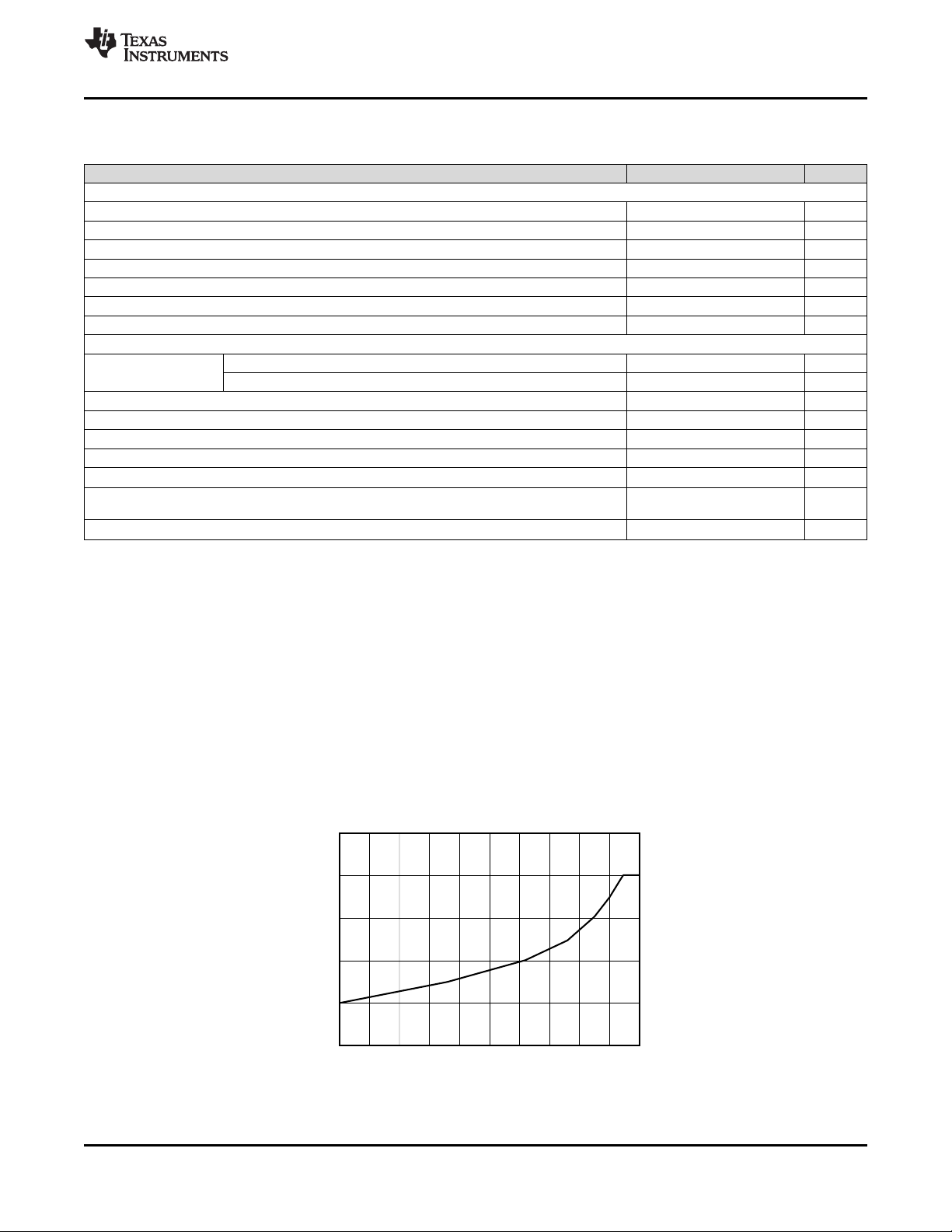
Micromirror Landed Duty Cycle
Operational (°C)
0/100 5/95 10/90 15/85 20/80 25/75 30/70 35/65 40/60 45/55
30
40
50
60
70
80
D001
50/50
100/0 95/5 90/10 85/15 80/20 75/25 70/30 65/35 60/40 55/45
Max Recommended Array Temperature –
DLP5500
www.ti.com
DLPS013G –APRIL 2010–REVISED JANUARY 2019
Recommended Operating Conditions (continued)
over operating free-air temperature range (unless otherwise noted)
MIN NOM MAX UNIT
LVDS INTERFACE
ƒ
clock
|VID| Input differential voltage (absolute value)
V
CM
V
LVDS
t
LVDS_RSTZ
Z
IN
Z
LINE
ENVIRONMENTAL
T
DMD
T
WINDOW
T
CERAMIC-WINDOW-DELTA
ILL
UV
ILL
VIS
ILL
IR
(9) Refer to Figure 5, Figure 6, and Figure 7.
(10) Optimal, long-term performance and optical efficiency of the Digital Micromirror Device (DMD) can be affected by various application
parameters, including illumination spectrum, illumination power density, micromirror landed duty-cycle, ambient temperature (storage
and operating), DMD temperature, ambient humidity (storage and operating), and power on or off duty cycle. TI recommends that
application-specific effects be considered as early as possible in the design cycle.
(11) DMD Temperature is the worst-case of any thermal test point in Figure 16, or the active array as calculated by the Micromirror Array
Temperature Calculation for Uniform Illumination.
(12) Per Figure 1, the maximum operational case temperature should be derated based on the micromirror landed duty cycle that the DMD
experiences in the end application. Refer to Micromirror Landed-on/Landed-Off Duty Cycle for a definition of micromirror landed duty
cycle.
(13) Long-term is defined as the average over the usable life of the device.
(14) Short-term is defined as less than 60 cumulative days over the over the usable life of the device.
(15) Window temperature as measured at thermal test points TP2, TP3, TP4 and TP5 in Figure 16.The locations of thermal test points TP2,
TP3, TP4 and TP5 in Figure 16 are intended to measure the highest window edge temperature. If a particular application causes
another point on the window edge to be at a higher temperature, a test point should be added to that location.
(16) Ceramic package temperature as measured at test point 1 (TP 1) in Figure 16.
(17) Dew points beyond the specified long-term dew point (operating, non-operating, or storage) are for short-term conditions only, where
short-term is defined as< 60 cumulative days over the usable life of the device.
(18) Refer to Thermal Information and Micromirror Array Temperature Calculation.
Clock frequency for LVDS interface, DCLK (all channels) 200 MHz
Common mode
LVDS voltage
(9)
(9)
(9)
100 400 600 mV
1200 mV
0 2000 mV
Time required for LVDS receivers to recover from PWRDNZ 10 ns
Internal differential termination resistance 95 105 Ω
Line differential impedance (PWB/trace) 90 100 110 Ω
(10)
(15)
(11) (12) (13)
(11) (14)
10 40 to 70
–20 75 °C
(15) (16)
Long-term DMD temperature (operational)
Short-term DMD temperature (operational)
Window temperature – operational
Delta ceramic-to-window temperature -operational
Long-term dew point (operational & non-operational) 24 °C
Short-term dew point
(13) (17)
(operational & non-operational) 28 °C
Illumination, wavelength < 420 nm 0.68
Illumination, wavelengths between 420 and 700 nm
Thermally
Limited
Illumination, wavelength > 700 nm 10
(12)
90 °C
30 °C
mW/cm
mW/cm
(18)
mW/cm
°C
2
2
2
Figure 1. Max Recommended DMD Temperature – Derating Curve
Product Folder Links: DLP5500
Submit Documentation FeedbackCopyright © 2010–2019, Texas Instruments Incorporated
9
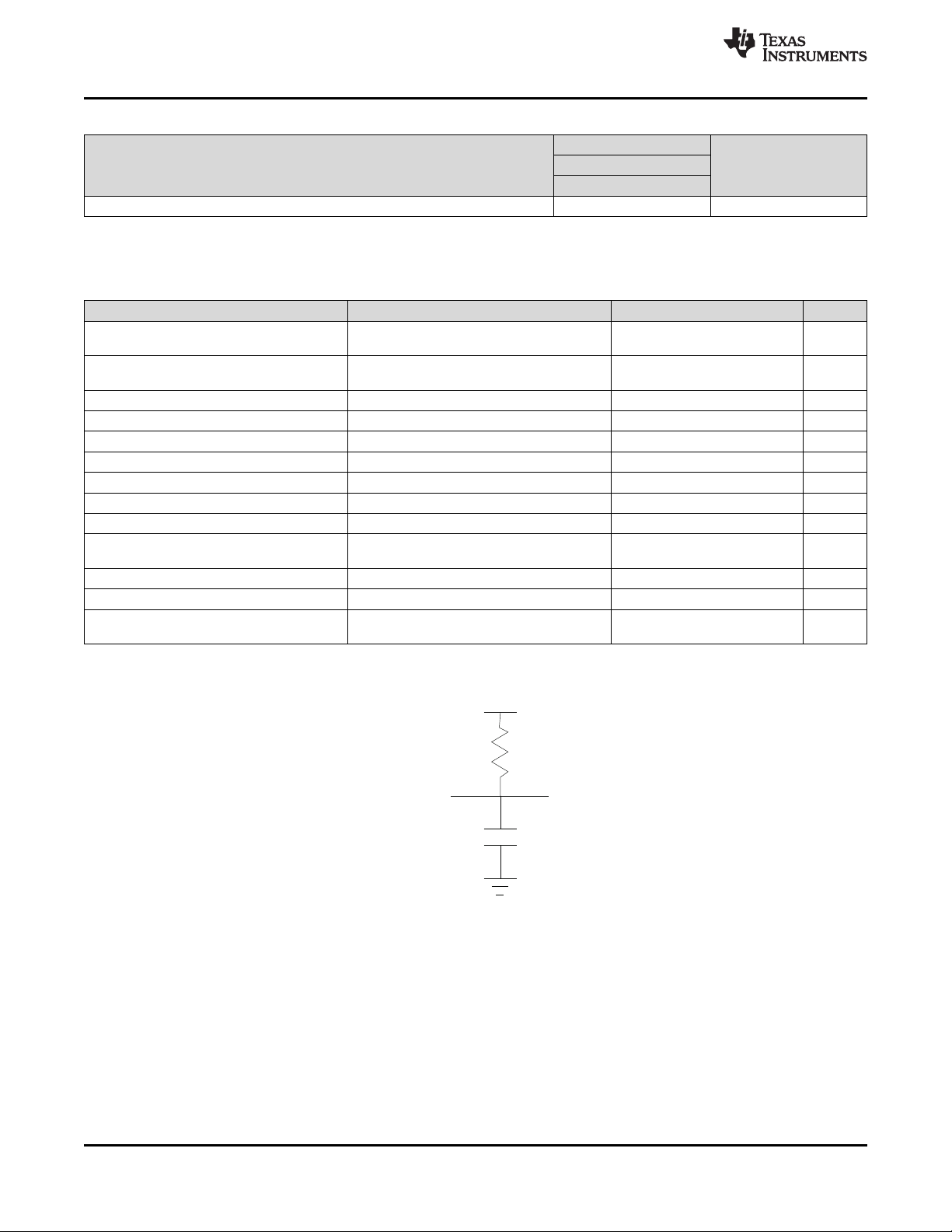
From Output
Under Test
Tester
Channel
LOAD CIRCUIT
C = 50 pF
C = 5 pF for Disable Time
L
L
R
L
DLP5500
DLPS013G –APRIL 2010–REVISED JANUARY 2019
8.5 Thermal Information
THERMAL METRIC
Thermal resistance from active array to specified point on case (TP1)
(1)
(1) For more information, see Micromirror Array Temperature Calculation.
8.6 Electrical Characteristics
over operating free-air temperature range (unless otherwise noted)
PARAMETER TEST CONDITIONS MIN TYP MAX UNIT
V
V
I
I
I
I
I
I
Z
Z
C
C
C
OH
OL
OZ
IL
IH
CC
CCI
CC2
IN
LINE
I
O
IM
High-level output voltage
Figure 2
Low-level output voltage
Figure 2
High impedance output current
Low-level input current
High-level input current
Current into VCCpin VCC= 3.6 V, 750 mA
Current into V
Current into V
OFFSET
CC2
Internal Differential Impedance 95 105 Ω
Line Differential Impedance (PWB
or Trace)
Input capacitance
Output capacitance
Input capacitance for
MBRST[0:15] pins
(1) Applies to LVCMOS pins only
(2) Exceeding the maximum allowable absolute voltage difference between VCCand V
Absolute Maximum Ratings for details)
(1)
, See
(1)
, See
(1)
(1)
(1)
(2)
pin
pin V
(1)
(1)
VCC= 3.0 V, IOH= –20 mA 2.4 V
VCC= 3.6 V, IOL= 15 mA 0.4 V
VCC= 3.6 V 10 µA
VCC= 3.6 V, VI= 0 V –60 µA
VCC= 3.6 V, VI= V
V
= 3.6 V 450 mA
CCI
= 8.75V 25 mA
CC2
CC
f = 1 MHz 10 pF
f = 1 MHz 10 pF
f = 1 MHz 160 210 pF
DLP5500
UNITFYA (CPGA)
149 PINS
0.6 °C/W
200 µA
90 100 110 Ω
may result in excess current draw. (Refer to
CCI
www.ti.com
10
Figure 2. Measurement Condition for LVCMOS Output
Submit Documentation Feedback Copyright © 2010–2019, Texas Instruments Incorporated
Product Folder Links: DLP5500
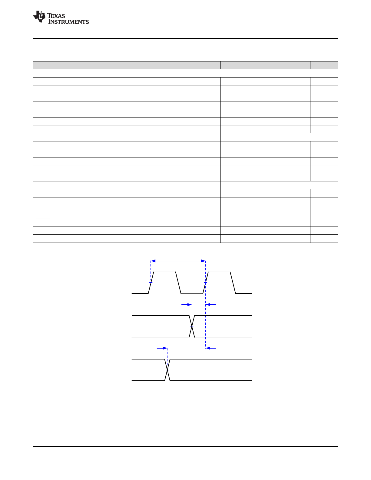
50% 50%
t
c
f
clock
= 1 / t
c
SCPCLK
SCPDI
50%
t
SCP_SKEW
SCPD0
50%
t
SCP_DELAY
DLP5500
www.ti.com
DLPS013G –APRIL 2010–REVISED JANUARY 2019
8.7 Timing Requirements
over operating free-air temperature range (unless otherwise noted)
MIN NOM MAX UNIT
LVDS TIMING PARAMETERS (See Figure 9)
t
c
t
w
t
s
t
s
t
h
t
h
t
skew
LVDS WAVEFORM REQUIREMENTS (See Figure 6)
|VID| Input Differential Voltage (absolute difference) 100 400 600 mV
V
CM
V
LVDS
t
r
t
r
SERIAL CONTROL BUS TIMING PARAMETERS (See Figure 3 and Figure 4)
f
SCP_CLK
t
SCP_SKEW
t
SCP_DELAY
t
SCP_EN
t
r_SCP
t
fP
Clock Cycle DLCK_A or DCLKC_B 5 ns
Pulse Width DCLK_A or DCLK_B 2.5 ns
Setup Time, D_A[0:15] before DCLK_A .35 ns
Setup Time, D_B[0:15] before DCLK_B .35 ns
Hold Time, D_A[0:15] after DCLK_A .35 ns
Hold Time, D_B[0:15] after DCLK_B .35 ns
Channel B relative to Channel A –1.25 1.25 ns
Common Mode Voltage 1200 mV
LVDS Voltage 0 2000 mV
Rise Time (20% to 80%) 100 400 ps
Fall Time (80% to 20%) 100 400 ps
SCP Clock Frequency 50 500 kHz
Time between valid SCP_DI and rising edge of SCP_CLK –300 300 ns
Time between valid SCP_DO and rising edge of SCP_CLK 2600 ns
Time between falling edge of SCP_EN and the first rising edge of
SCP_CLK
30 ns
Rise time for SCP signals 200 ns
Fall time for SCP signals 200 ns
Figure 3. Serial Communications Bus Timing Parameters
Product Folder Links: DLP5500
Submit Documentation FeedbackCopyright © 2010–2019, Texas Instruments Incorporated
11
V /2
CC
0 v
SCP_CLK,
SCP_DI,
SCP_EN
Input Controller V
CC
t
r_SCP
t
f_SCP
DLP5500
DLPS013G –APRIL 2010–REVISED JANUARY 2019
Figure 4. Serial Communications Bus Waveform Requirements
www.ti.com
12
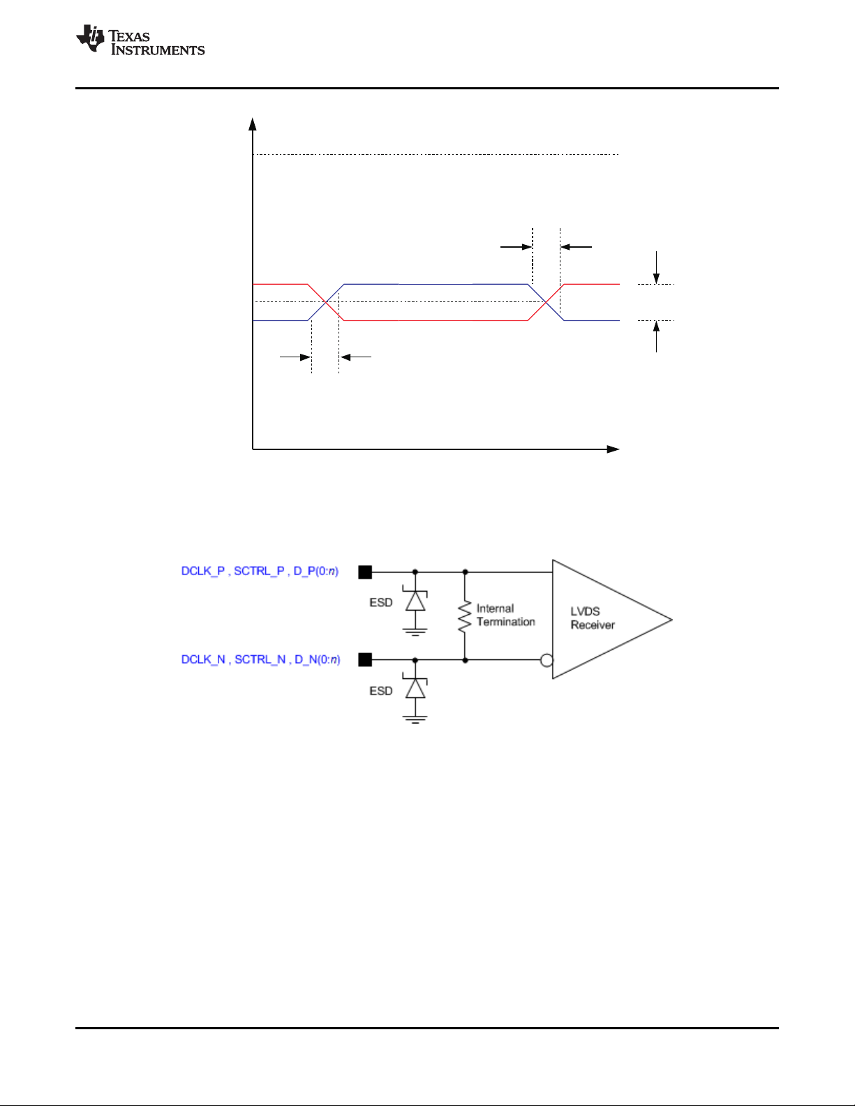
Refer to LVDS Interface section of the Recommended Operating Conditions.
Refer to Pin Configuration and Functions for list of LVDS pins.
Figure 5. LVDS Voltage Definitions (References)
Submit Documentation Feedback Copyright © 2010–2019, Texas Instruments Incorporated
Product Folder Links: DLP5500
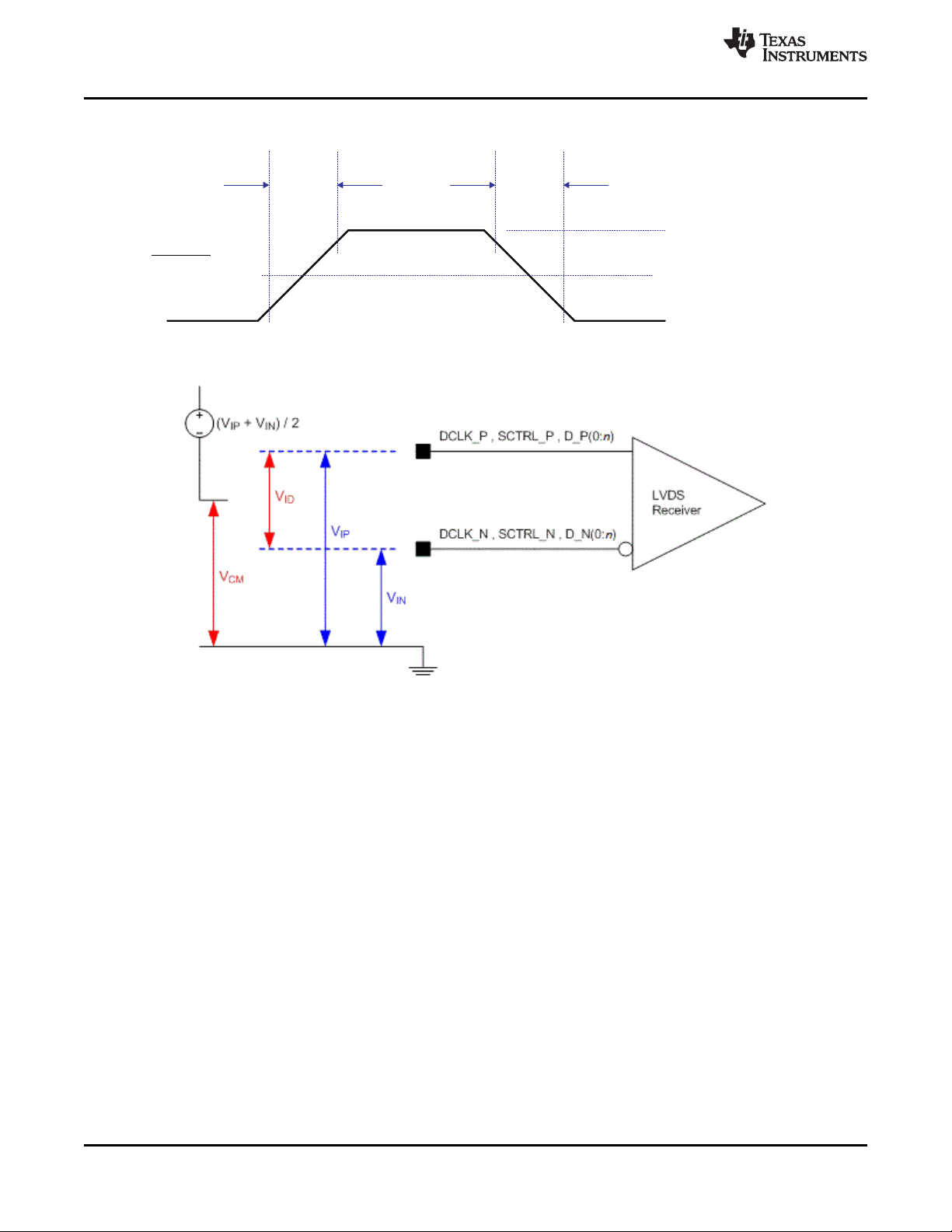
V
CM
V
LVDS
(v)
V
ID
Tr(20% - 80%)
Tf(20% - 80%)
Time
V
LVDSmax
V
LVDS min
V = V + |½V |
IDLVDSmax CM
V
LVDS
= VCM+/- | 1/2 VID|
V
LVDS min
= 0
www.ti.com
DLP5500
DLPS013G –APRIL 2010–REVISED JANUARY 2019
Not to scale.
Refer to LVDS Interface section of the Recommended Operating Conditions.
Figure 6. LVDS Waveform Requirements
Refer to LVDS Interface section of the Recommended Operating Conditions.
Refer to Pin Configuration and Functions for list of LVDS pins.
Figure 7. LVDS Equivalent Input Circuit
13
Submit Documentation FeedbackCopyright © 2010–2019, Texas Instruments Incorporated
Product Folder Links: DLP5500
SCTRL_AN
SCTRL_AP
D_AN(15:0)
D_AP(15:0)
D_BN(15:0)
D_BP(15:0)
DCLK_BN
DCLK_BP
SCTRL_BN
SCTRL_BP
DCLK_AN
DCLK_AP
Tw
Tc
Tw
Th
Th
Ts
Ts
Tskew
Tw
Tc
Tw
Th
Th
Ts
Ts
0.0 * VCC
1.0 * VCC
t
f
t
r
1.0 * V
ID
0.0 * V
ID
V
CM
t
f
t
r
LVDS Interface SCP Interface
DLP5500
DLPS013G –APRIL 2010–REVISED JANUARY 2019
Not to scale.
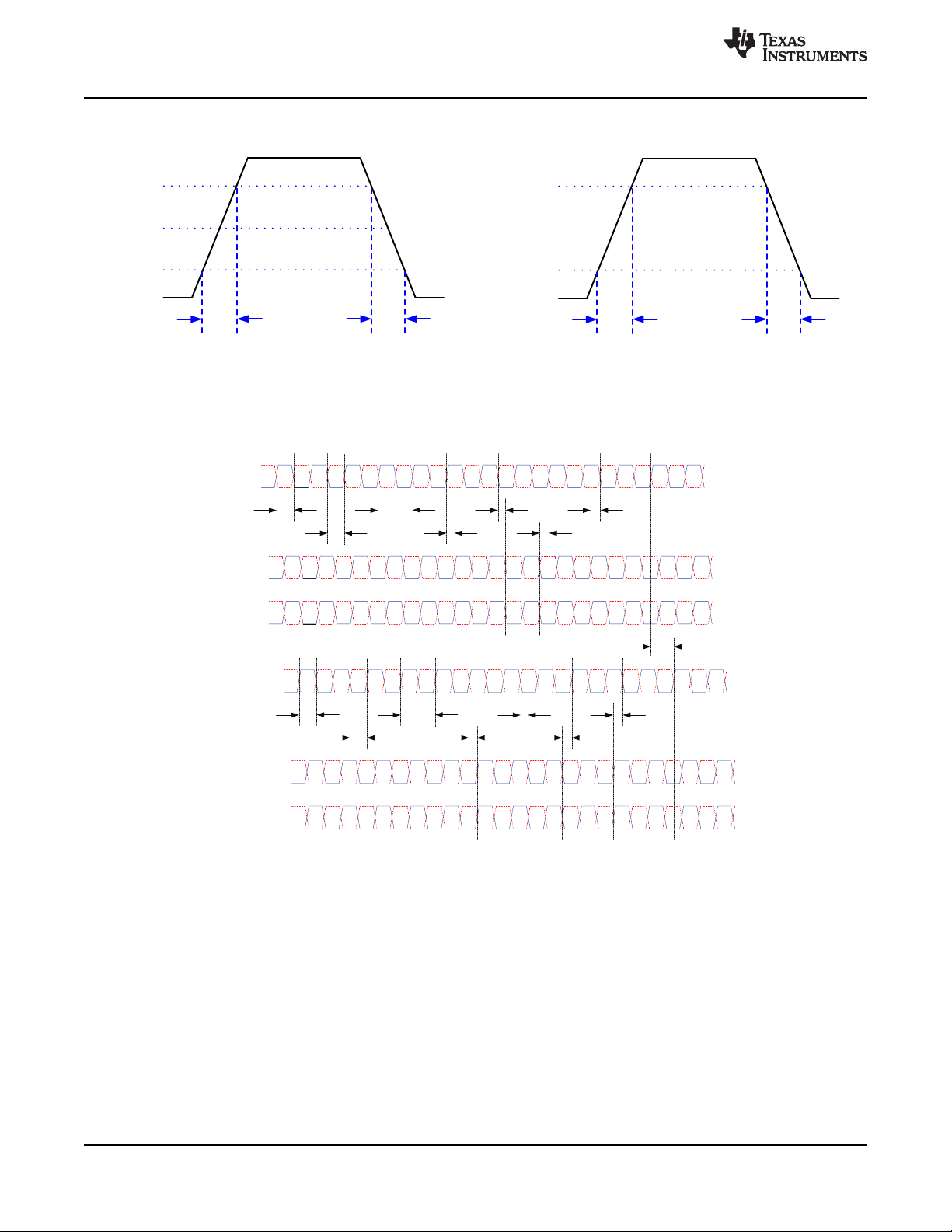
Refer to the Timing Requirements.
Refer to Pin Configuration and Functions for list of LVDS pins and SCP pins.
www.ti.com
Figure 8. Rise Time and Fall Time
Figure 9. LVDS Timing Waveforms
14
Submit Documentation Feedback Copyright © 2010–2019, Texas Instruments Incorporated
Product Folder Links: DLP5500
 Loading...