

Texas Instruments CY74FCT2646ATQC, CY74FCT2646CTQCT, CY74FCT2646CTQC, CY74FCT2646ATQCT Datasheet
8-Bit Registered Transceive
r
CY74FCT2646T
SCCS043 - September 1994 - Revised March 2000
Data sheet acquired from Cypress Semiconductor Corporation.
Data sheet modified to remove devices not offered.
Copyright © 2000, Texas Instruments Incorporated
Features
• Function and pinout compatible with FCT and F logic
• FCT-C speed at 5.4 ns max.
FCT-A speed at 6.3 ns max.
• Reduced V
OH
(typically = 3.3V) versions of equivalent
FCT functions
• 25Ωoutputseriesresistorstoreducetransmissionline
reflection noise
• Reduced V
OH
(typically=3.3V) versions of equivalent
FCT functions
• Edge-rate control circuitry for significantly improved
noise characteristics
• Power-off disable feature permits live insertion
• Matched rise and fall times
• ESD > 2000V
• Fully compatible with TTL input and output logic levels
• Sink current 12 mA
Source current 15 mA
• Independent register for A and B buses
• Extended commercial temp. range of –40˚C to +85˚C
• Three-state output
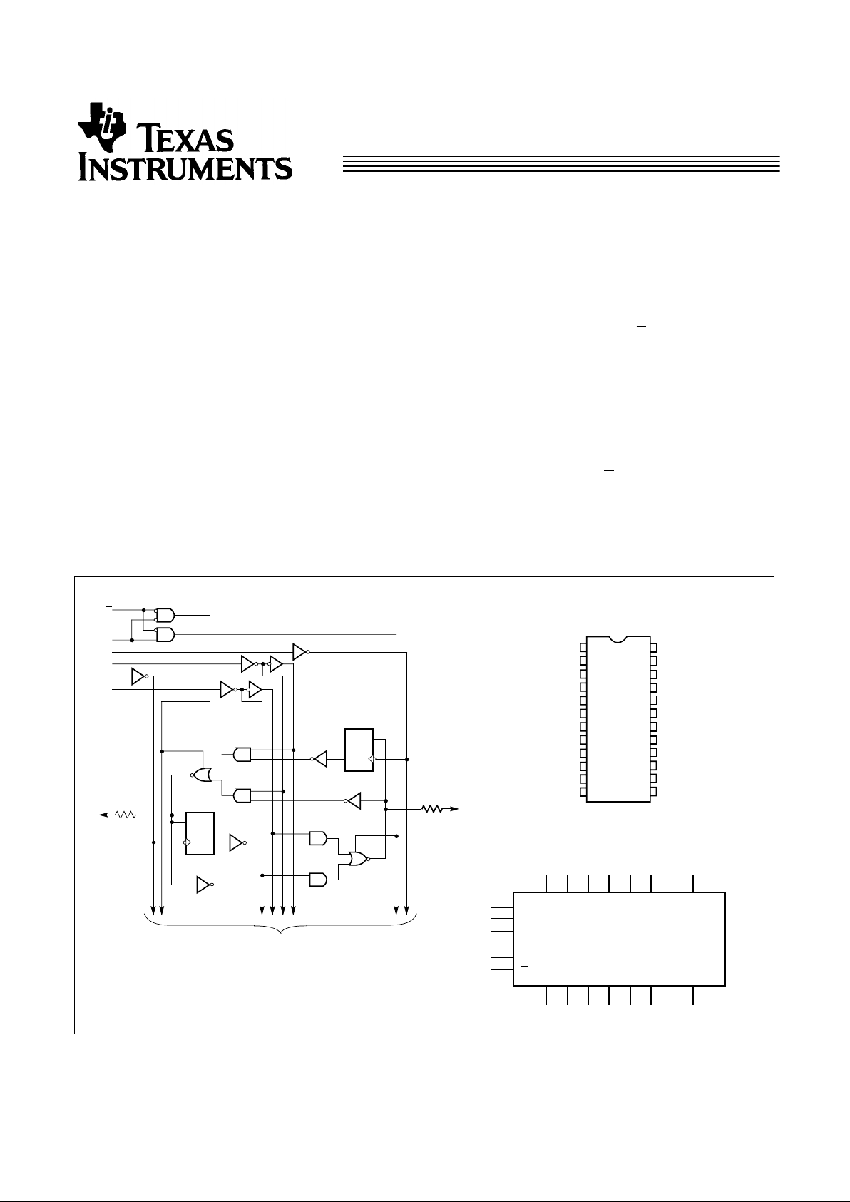
Functional Description
The FCT2646T consists of a bus transceiver circuit with
three-state, D-type flip-flops, and control circuitry arranged for
multiplexedtransmission of data directly from the input bus or
from the internal registers. Data on the A or B bus will be
clocked into the registers as the appropriate clock pin goes to
a HIGH logic level. Enable Control
G and direction pins are
provided to control the transceiver function. On-chip terminationresistorshavebeenadded to the outputs toreduce system
noisecaused by reflections sothat the FCT2646Tcan be used
to replace the FCT646T in an existing design.
In the transceiver mode, data present at the high impedance
port may be stored in either the A or B register, or in both.
Select controls can multiplexstored and real-time (transparent
mode) data. The direction control determines which bus will
receive data when the enable control
G is Active LOW. In the
isolation mode (enable control
G HIGH), A data may be stored
in the B register and/or B data may be stored in the A register.
The outputs are designed with a power-off disable feature to
allow for liv e insertion of boards.
LogicBlock Diagram
P
i
n
C
onfigurations
FCT2646T
–1
C
D
B
1
C
D
A
1
TO 7 OTHERCHANNELS
SAB
CPAB
CPBA
DIR
SBA
G
Functional Block Diagram
1
2
3
4
5
6
7
8
9
10
11
12
16
17
18
19
20
24
23
22
21
13
14
V
CC
FCT2646T–3
15
QSOP
Top View
CPAB
A
1
A
2
A
3
A
4
A
5
A
6
A
7
A
8
B
1
B
2
B
3
B
4
B
5
B
6
B
7
B
8
CPBA
SAB
SBA
DIR
G
GND
FCT2646T–4
CPAB
A
1A2A3A4A5A6A7A8
B1B2B3B4B5B6B7B
8
CPBA
SAB
SBA
DIR
G
CY74FCT2646T
2
Pin Description
Name Description
A Data Register A Inputs, Data Register B Outputs
B Data Register B Inputs, Data Register A Outputs
CPAB, CPBA Clock Pulse Inputs
SAB, SBA Output Data Source Select Inputs
DIR, G Output Enable Inputs
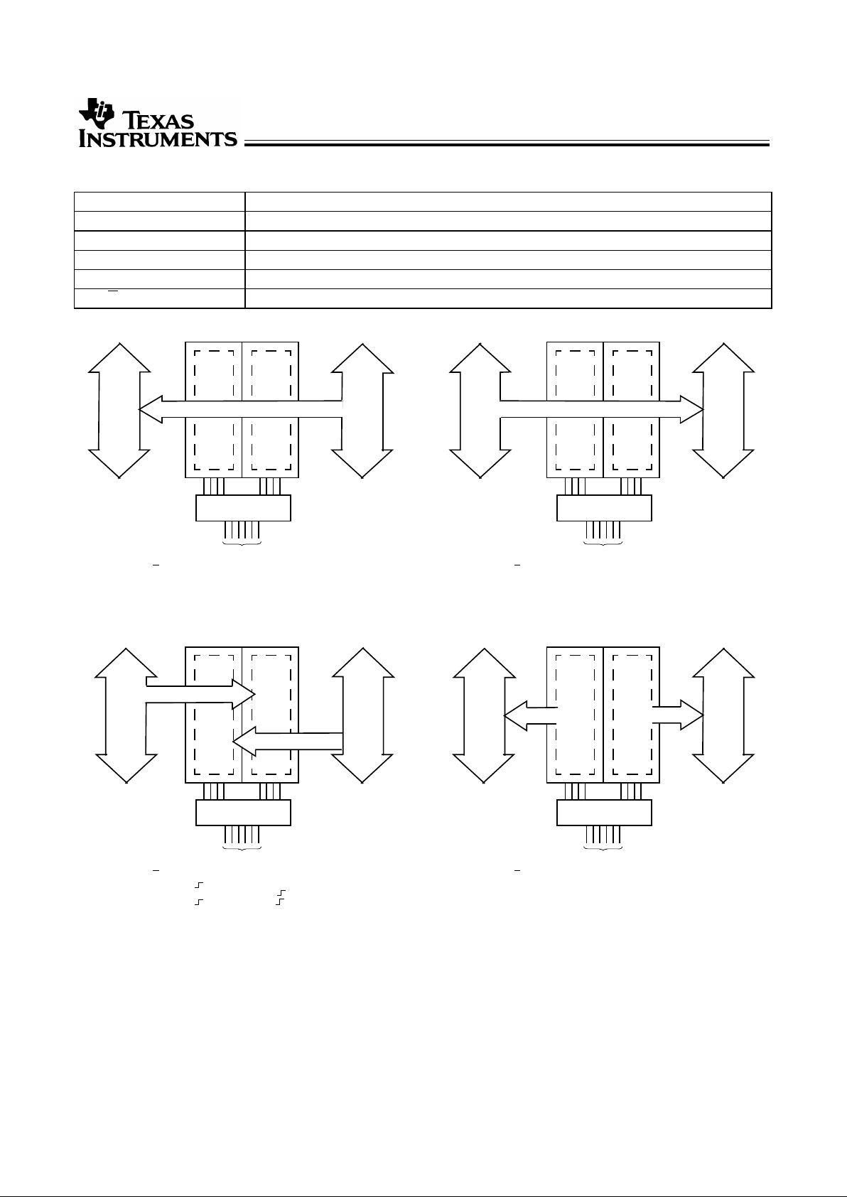
Note:
1. Cannot transfer data to A bus and B bus simultaneously.
BUS BBUS A
DIR
L
GLCPAB
X
CPBAXSABXSBA
X
BUS BBUS A
DIR
H
L
X
G
L
L
H
CPAB
X
CPBAXSAB
X
X
X
SBA
X
X
X
BUS
BBUS A
DIR
H
GLCPAB
X
CPBAXSABLSBA
X
BUS ABUS A
DIR
L
H
G
L
L
CPAB
X
HorL
CPBA
HorL
X
SAB
X
H
SBA
H
X
Real-TimeTransfer
Bus B to Bus A
Real-TimeTransfer
Bus A to Bus B
Storage from
A and/or B
Transfer Stored Data
to A and/or B
[1]
CY74FCT2646T
3
Maximum Ratings
[4, 5]
(Above which the useful life may be impaired. For user guidelines, not tested.)
Storage Temperature .................................–65°C to +150°C
Ambient Temperature with
Power Applied.............................................–65°C to +135°C
Supply Voltage to Ground Potential............... –0.5V to +7.0V
DC Input Voltage............................................–0.5V to +7.0V
DC Output Voltage......................................... –0.5V to +7.0V
DC Output Current (Maximum Sink Current/Pin) ......120 mA
Power Dissipation..........................................................0.5W
Static Discharge Voltage............................................>2001V
(per MIL-STD-883, Method 3015)
Function Table
[2]
Inputs Data I/O
[3]
Operation or Function
G DIR CPAB CPBA SAB SBA A1 thru A
8
B1 thru B
8
FCT2646T
H
H
X
X
H or L H or L X
X
X
X
Input Input Isolation
Store A and B Data
L
L
L
L
X
X
X
H or L
X
X
L
H
Output Input Real Time B Data to A Bus
Stored B Data to A Bus
L
L
H
H
X
H or L
X
X
L
H
X
X
Input Output Real Time A Data to B Bus
Stored A Data to B Bus
Operating Range
Range
Ambient
Temperature V
CC
Commercial –40°C to +85°C 5V ± 5%
Electrical Characteristics Over the Operating Range
Parameter Description Test Conditions Min. Typ
[6]
Max. Unit
V
OH
Output HIGH Voltage VCC=Min., IOH=–15 mA 2.4 3.3 V
V
OL
Output LOW Voltage VCC=Min., IOL=12 mA 0.3 0.55 V
R
OUT
Output Resistance VCC=Min., IOL=12 mA 20 25 40 Ω
V
IH
Input HIGH Voltage 2.0 V
V
IL
Input LOW Voltage 0.8 V
V
H
Hysteresis
[7]
All inputs 0.2 V
V
IK
Input Clamp Diode Voltage VCC=Min., IIN=–18 mA –0.7 –1.2 V
I
IH
Input HIGH Current VCC=Max., VIN=V
CC
5 µA
I
IH
Input HIGH Current VCC=Max., VIN=2.7V ±1 µA
I
IL
Input LOW Current VCC=Max., VIN=0.5V ±1 µA
I
OS
Output Short Circuit Current
[8]
VCC=Max., V
OUT
=0.0V –60 –120 –225 mA
I
OFF
Power-Off Disable VCC=0V, V
OUT
=4.5V ±1 µA
Notes:
2. H = HIGH Voltage Level. L = LOW Voltage Level. X = Don’t Care.
3. The data output functions may be enabled or disabled by various signals at the G or DIR inputs. Data input functions are always enabled,i.e.,data at the bus
pins will be stored on every LOW-to-HIGH transition of the clock inputs.
4. Unless otherwise noted, these limits are over the operating free-air temperature range.
5. Unused inputs must always be connected to an appropriate logic voltage level, preferably either V
CC
or ground.
6. Typical values are at VCC=5.0V, TA=+25˚C ambient.
7. This parameter is specified but not tested.
8. Not more than one output should be shorted at a time. Duration of short should not exceed one second. The use of high-speed test apparatus and/or sample
and hold techniques are preferable in order to minimize internal chip heating and more accurately reflect operational values. Otherwise prolonged shorting
ofahigh output may raise thechiptemperature well abovenormal andthereby cause invalid readingsin other parametric tests. In anysequenceof parameter
tests, IOS tests should be performed last.

CY74FCT2646T
4
Capacitance
[7]
Parameter Description Typ.
[6]
Max. Unit
C
IN
Input Capacitance 6 10 pF
C
OUT
Output Capacitance 8 12 pF
Power Supply Characteristics
Parameter Description Test Conditions Typ.
[6]
Max. Unit
I
CC
Quiescent Power Supply Current VCC=Max., VIN≤0.2V,
V
IN≥VCC
–0.2V
0.1 0.2 mA
∆I
CC
Quiescent Power Supply Current
(TTL inputs HIGH)
VCC=Max., VIN=3.4V,
[9]
f1=0, Outputs Open
0.5 2.0 mA
I
CCD
Dynamic Power Supply Current
[10]
VCC=Max., One Input Toggling,
50% Duty Cycle, Outputs Open,
G=DIR=GND, GAB=GBA=GND,
V
IN
≤0.2V or VIN≥VCC–0.2V
0.06 0.12 mA/
MHz
I
C
Total Power Supply Current
[11]
VCC=Max., f0=10 MHz,
50% Duty Cycle, Outputs Open,
One Bit Toggling at f
1
=5 MHz,
G=DIR=GND, GAB=GBA=GND,
V
IN
≤0.2V or VIN≥VCC–0.2V
0.7 1.4 mA
VCC=Max., f0=10 MHz,
50% Duty Cycle, Outputs Open,
One Bit Toggling at f
1
=5 MHz,
G=DIR=GND, GAB=GBA=GND,
V
IN
=3.4V or VIN=GND
1.2 3.4 mA
VCC=Max., f0=10 MHz,
50% Duty Cycle, Outputs Open,
Eight Bits Toggling at f
1
=5 MHz,
G=DIR=GND, GAB=GBA=GND,
V
IN
≤0.2V or VIN≥VCC–0.2V
2.8 5.6
[12]
mA
VCC=Max., f0=10 MHz,
50% Duty Cycle, Outputs Open,
Eight Bits Toggling at f
1
=5 MHz,
G=DIR=GND, GAB=GBA=GND,
V
IN
=3.4V or VIN=GND
5.1 14.6
[12]
mA
Notes:
9. Per TTL driven input (V
IN
=3.4V); all other inputs at VCC or GND.
10. This parameter is not directly testable, but is derived for use in Total Power Supply calculations.
11. I
C
=I
QUIESCENT
+ I
INPUTS
+ I
DYNAMIC
IC=ICC+∆ICCDHNT+I
CCD(f0
/2 + f1N1)
I
CC
= Quiescent Current with CMOS input levels
∆I
CC
= Power Supply Current for a TTL HIGH input (VIN=3.4V)
D
H
= Duty Cycle for TTL inputs HIGH
N
T
= Number of TTL inputs at D
H
I
CCD
= Dynamic Current caused by an input transition pair (HLH or LHL)
f
0
= Clock frequency for registered devices, otherwise zero
f
1
= Input signal frequency
N
1
= Number of inputs changing at f
1
All currents are in milliamps and all frequencies are in megahertz.
12. Values for these conditions are examples of the ICC formula. These limits are specified but not tested.

CY74FCT2646T
5
Switching Characteristics Over the Operating Range
[13]
Parameter Description
CY74FCT2646AT CY74FCT2646CT
Unit Fig. No.
[14]
Min. Max. Min. Max.
t
PLH
t
PHL
Propagation Delay Bus to Bus 1.5 6.3 1.5 5.4 ns 1, 3
t
PZH
t
PZL
Output Enable Time Enable to
Bus and DIR to A
n
or B
n
1.5 9.8 1.5 7.8 ns 1, 7, 8
t
PHZ
t
PLZ
Output Disable Time
G to Bus and DIR to Bus
1.5 6.3 1.5 6.3 ns 1, 7, 8
t
PLH
t
PHL
Propagation Delay
Clock to Bus
1.5 6.3 1.5 5.7 ns 1, 5
t
PLH
t
PHL
Propagation Delay
SBA or SAB to A or B
1.5 7.7 1.5 6.2 ns 1, 5
t
S
Set-Up Time HIGH or LOW, Bus
to Clock
2.0 2.0 ns 4
t
H
Hold Time HIGH or LOW,
Bus to Clock
1.5 1.5 ns 4
t
W
Pulse Width,
[7]
HIGH or LOW
5.0 5.0 ns 5
Notes:
13. Minimum limits are specified but not tested on Propagation Delays.
14. See “Parameter Measurement Information” in the General Information section.
Ordering Information
Speed
(ns) Ordering Code
Package
Name Package Type
Operating
Range
5.4 CY74FCT2646CTQCT Q13 24-Lead (150-Mil) QSOP Commercial
6.3 CY74FCT2646ATQCT Q13 24-Lead (150-Mil) QSOP Commercial
Document #: 38-00599

CY74FCT2646T
6
Package Diagrams
24-Lead Quarter Size Outline Q13

IMPORTANT NOTICE
T exas Instruments and its subsidiaries (TI) reserve the right to make changes to their products or to discontinue
any product or service without notice, and advise customers to obtain the latest version of relevant information
to verify, before placing orders, that information being relied on is current and complete. All products are sold
subject to the terms and conditions of sale supplied at the time of order acknowledgement, including those
pertaining to warranty, patent infringement, and limitation of liability.
TI warrants performance of its semiconductor products to the specifications applicable at the time of sale in
accordance with TI’s standard warranty. Testing and other quality control techniques are utilized to the extent
TI deems necessary to support this warranty. Specific testing of all parameters of each device is not necessarily
performed, except those mandated by government requirements.
CERT AIN APPLICATIONS USING SEMICONDUCTOR PRODUCTS MAY INVOLVE POTENTIAL RISKS OF
DEATH, PERSONAL INJURY, OR SEVERE PROPERTY OR ENVIRONMENTAL DAMAGE (“CRITICAL
APPLICATIONS”). TI SEMICONDUCTOR PRODUCTS ARE NOT DESIGNED, AUTHORIZED, OR
WARRANTED TO BE SUITABLE FOR USE IN LIFE-SUPPORT DEVICES OR SYSTEMS OR OTHER
CRITICAL APPLICATIONS. INCLUSION OF TI PRODUCTS IN SUCH APPLICA TIONS IS UNDERSTOOD T O
BE FULLY AT THE CUSTOMER’S RISK.
In order to minimize risks associated with the customer’s applications, adequate design and operating
safeguards must be provided by the customer to minimize inherent or procedural hazards.
TI assumes no liability for applications assistance or customer product design. TI does not warrant or represent
that any license, either express or implied, is granted under any patent right, copyright, mask work right, or other
intellectual property right of TI covering or relating to any combination, machine, or process in which such
semiconductor products or services might be or are used. TI’s publication of information regarding any third
party’s products or services does not constitute TI’s approval, warranty or endorsement thereof.
Copyright 2000, Texas Instruments Incorporated
 Loading...