Texas Instruments CY74FCT2543TQCT, CY74FCT2543TQC, CY74FCT2543CTSOCT, CY74FCT2543CTSOC, CY74FCT2543CTQCT Datasheet
...
8-Bit Latched Transceive
r
CY74FCT2543T
SCCS042 - September 1994 - Revised March 2000
Data sheet acquired from Cypress Semiconductor Corporation.
Data sheet modified to remove devices not offered.
Copyright © 2000, Texas Instruments Incorporated
Features
• Function and pinout compatible with FCT and F logic
• FCT-C speed at 5.3 ns max.
FCT-A speed at 6.5 ns max.
• 25Ωoutputseriesresistorstoreducetransmissionline
reflection noise
• Reduced V
OH
(typically = 3.3V) versions of equivalent
FCT functions
• Edge-rate control circuitry for significantly improved
noise characteristics
• Power-off disable feature
• Matched rise and fall times
• Fully compatible with TTL input and output logic levels
• Sink current 12 mA
Source current 15 mA
• Separation controls for data flow in each direction
• Back to back latches for storage
• ESD > 2000V
• Extended commercial temp. range of –40˚C to +85˚C
Functional Description
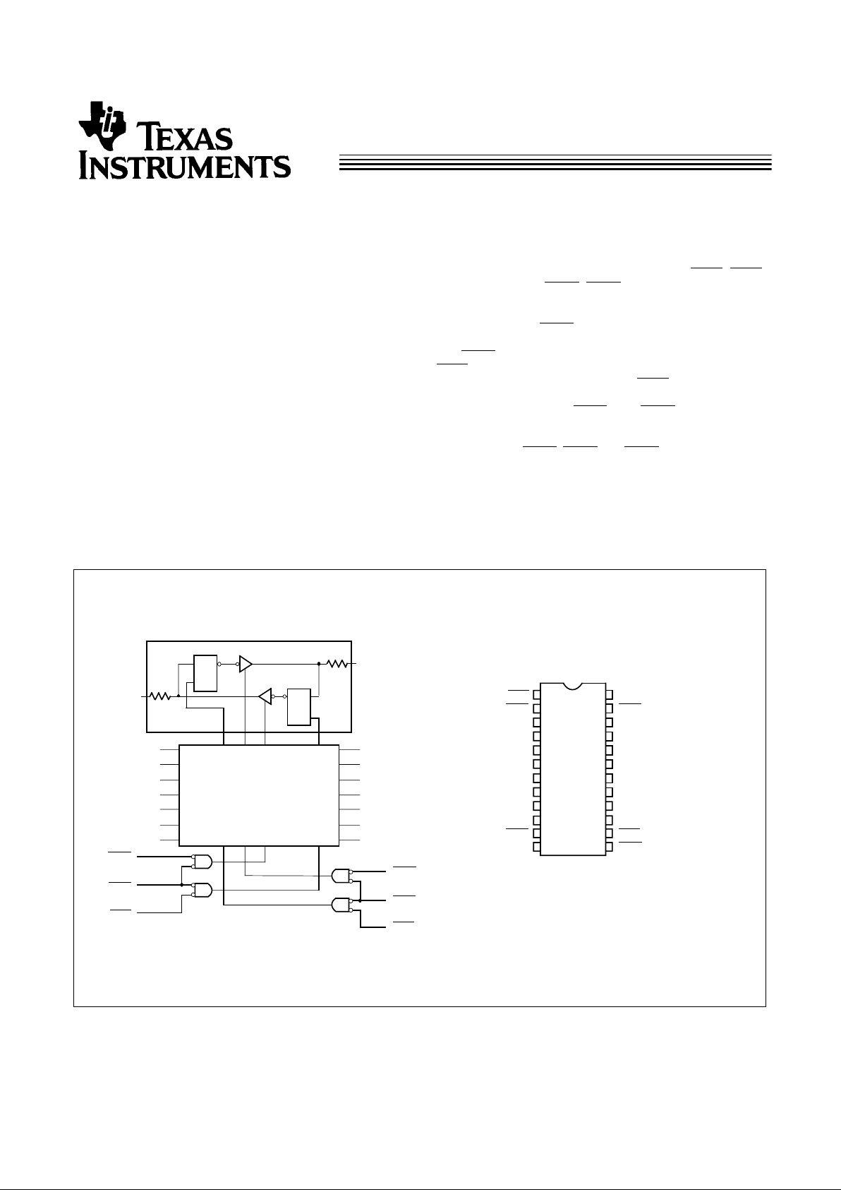
The FCT2543T Octal Latched Tranceiver contains two sets of
eight D-type latches. Separate Latch Enable (
LEAB, LEBA)
and Output Enable (
OEAB, OEBA) permits each latch set to
have independent control of inputting and outputting in either
direction of data flow. For data flow from A to B, for example,
the A-to-B Enable (
CEAB) input must be LOW to enter data
from A or to take data from B, as indicated in the truth table.
With
CEAB LOW, a LOW signal on the A-to-B Latch Enable
(
LEAB) input makes the A-to-B latches transparent; a subse-
quent LOW-to-HIGH transition of the
LEAB signal puts the A
latches in the storage mode and their output no longer change
with the A inputs. With
CEAB and OEAB both LOW, the
three-state B output buffersare active and reflect data present
at the output of the A latches. Control of data from B to A is
similar,but uses
CEAB, LEAB, and OEAB inputs. On-chip termination resistors have been added to the outputs to reduce
system noise caused by reflections. The FCT2543T can be
used to replace the FCT543T to reduce noise in an existing
design.
The outputs are designed with a power-off disable feature to
allow for liv e insertion of boards.
FCT2543T–1
LE
D
Q
LE
DQ
Detail A
Detail A x 7
A
0
A
2
A
1
A
3
A
4
A
6
A
5
A
7
B
0
B
2
B
1
B
3
B
4
B
6
B
5
B
7
OEBA
CEBA
LEBA
OEAB
CEAB
LEAB
FunctionalBlock Diagram Pin Configurations
1
2
3
4
5
6
7
8
9
10
11
12
16
17
18
19
20
24
23
22
21
13
14
V
CC
FCT2543T–3
15
SOIC/QSOP
Top View
LEBA
A
1
A
2
A
3
A
4
A
5
A
6
A
7
CEAB
B
1
B
2
B
3
B
4
B
5
B
6
B
7
OEAB
CEBAOEBA
A
0
GND
B
0
LEAB

CY74FCT2543T
2
Maximum Ratings
[4,5]
(Above which theuseful life may be impaired. For user guidelines, not tested.)
Storage Temperature .....................................−65°C to +150°C
Ambient Temperature with
Power Applied..................................................−65°C to +135°C
Supply Voltage to Ground Potential..................−0.5V to +7.0V
DC Input Voltage .................................................−0.5V to +7.0V
DC Output Voltage..............................................−0.5V to +7.0V
DC Output Current (Maximum Sink Current/Pin) ......120 mA
Power Dissipation..........................................................0.5W
Static Discharge Voltage............................................>2001V
(per MIL-STD-883, Method 3015)
Pin Description
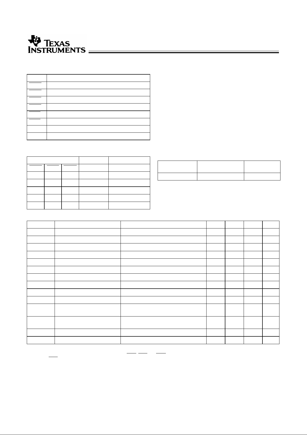
Name Description
OEAB A-to-B Output Enable Input (Active LOW)
OEBA B-to-A Output Enable Input (Active LOW)
CEAB A-to-B Enable Input (Active LOW)
CEBA B-to-A Enable Input (Active LOW)
LEAB A-to-B Latch Enable Input (Active LOW)
LEBA B-to-A Latch Enable Input (Active LOW)
A A-to-B Data Inputs or B-to-A Three-State Outputs
B B-to-A Data Inputs or A-to-B Three-State Outputs
Function Table
[1,2]
Inputs Latch Outputs
CEAB LEAB OEAB A-to-B
[3]
B
H X X Storing High Z
X H X Storing X
X X H X High Z
L L L Transparent Current A Inputs
L H L Storing Previous A Inputs
Operating Range
Range
Ambient
Temperature V
CC
Commercial −40°C to +85°C 5V ± 5%
Electrical Characteristics Over the Operating Range
Parameter Description Test Conditions Min. Typ.
[7]
Max. Unit
V
OH
Output HIGH Voltage VCC=Min., IOH=−15 mA 2.4 3.3 V
V
OL
Output LOW Voltage VCC=Min., IOL=12 mA 0.3 0.55 V
R
OUT
Output Resistance VCC=Min., IOL=12 mA 20 25 40 Ω
V
IH
Input HIGH Voltage 2.0 V
V
IL
Input LOW Voltage 0.8 V
V
H
Hysteresis
[8]
All inputs 0.2 V
V
IK
Input Clamp Diode Voltage VCC=Min., IIN=−18 mA −0.7 −1.2 V
I
IH
Input HIGH Current VCC=Max., VIN=V
CC
5 µA
I
IH
Input HIGH Current VCC=Max., VIN=2.7V ±1 µA
I
IL
Input LOW Current VCC=Max., VIN=0.5V ±1 µA
I
OZH
Off State HIGH-Level Output
Current
VCC=Max., V
OUT
=2.7V 15 µA
I
OZL
Off State LOW-Level
Output Current
VCC=Max., V
OUT
=0.5V −15 µA
I
OS
Output Short Circuit Current
[9]
VCC=Max., V
OUT
=0.0V −60 −120 −225 mA
I
OFF
Power-Off Disable VCC=0V, V
OUT
=4.5V ±1 µA
Notes:
1. H = HIGH Voltage Level. L = LOW Voltage Level. X = Don’t Care.
2. A-to-B data flow shown: B-to-A is the same, except using
CEBA, LEBA, and OEBA.
3. Before LEAB LOW-to-HIGH transition.
4. Unless otherwise noted, these limits are over the operating free-air temperature range.
5. Unused inputs must always be connected to an appropriate logic voltage level, preferably either VCC or ground.
6. T
A
is the “instant on” case temperature.
 Loading...