

Page 1
Service Manual
Tektronix
TDS 620A, 640A & 644A
Digitizing Oscilloscope
070-8718-04
Warning
The servicing instructions are for use by qualified
personnel only. To avoid personal injury, do not
perform any servicing unless you are qualified to
do so. Refer to all safety summaries prior to
performing service.
Page 2

Copyright © Tektronix, Inc. 1993. All rights reserved.
Tektronix products are covered by U.S. and foreign patents, issued and pending. Information in this publication supercedes
that in all previously published material. Specifications and price change privileges reserved.
Printed in the U.S.A.
Tektronix, Inc., P.O. Box 1000, Wilsonville, OR 97070-1000
TEKTRONIX and TEK are registered trademarks of Tektronix, Inc.
Page 3

WARRANTY
Tektronix warrants that the products that it manufactures and sells will be free from defects in materials and
workmanship for a period of three (3) years from the date of shipment. If a product proves defective during this
warranty period, Tektronix, at its option, either will repair the defective product without charge for parts and labor,
or will provide a replacement in exchange for the defective product.
In order to obtain service under this warranty, Customer must notify Tektronix of the defect before the expiration
of the warranty period and make suitable arrangements for the performance of service. Customer shall be
responsible for packaging and shipping the defective product to the service center designated by Tektronix, with
shipping charges prepaid. Tektronix shall pay for the return of the product to Customer if the shipment is to a
location within the country in which the Tektronix service center is located. Customer shall be responsible for
paying all shipping charges, duties, taxes, and any other charges for products returned to any other locations.
This warranty shall not apply to any defect, failure or damage caused by improper use or improper or inadequate
maintenance and care. Tektronix shall not be obligated to furnish service under this warranty a) to repair damage
resulting from attempts by personnel other than Tektronix representatives to install, repair or service the product;
b) to repair damage resulting from improper use or connection to incompatible equipment; c) to repair any
damage or malfunction caused by the use of non-Tektronix supplies; or d) to service a product that has been
modified or integrated with other products when the effect of such modification or integration increases the time
or difficulty of servicing the product.
THIS WARRANTY IS GIVEN BY TEKTRONIX IN LIEU OF ANY OTHER WARRANTIES, EXPRESS
OR IMPLIED. TEKTRONIX AND ITS VENDORS DISCLAIM ANY IMPLIED WARRANTIES OF
MERCHANTABILITY OR FITNESS FOR A PARTICULAR PURPOSE. TEKTRONIX'
RESPONSIBILITY TO REPAIR OR REPLACE DEFECTIVE PRODUCTS IS THE SOLE AND
EXCLUSIVE REMEDY PROVIDED TO THE CUSTOMER FOR BREACH OF THIS WARRANTY.
TEKTRONIX AND ITS VENDORS WILL NOT BE LIABLE FOR ANY INDIRECT, SPECIAL,
INCIDENTAL, OR CONSEQUENTIAL DAMAGES IRRESPECTIVE OF WHETHER TEKTRONIX OR
THE VENDOR HAS ADVANCE NOTICE OF THE POSSIBILITY OF SUCH DAMAGES.
Page 4

Page 5
Specifications
Table of Contents
List of Figures vii
List of Tables xi
Safety Summary xiii
Specifications 1-1
General Product Description 1-1
User Interface 1-2
Menus 1-2
Indicators 1-2
General Purpose Knob 1-2
GUI 1-2
Signal Acquisition System 1-3
Horizontal System 1-3
Trigger System 1-4
Acquisition Control 1-4
On-Board User Assistance 1-5
Help 1-5
Autoset 1-5
Measurement Assistance 1-5
Cursor 1-5
Measure 1-5
Digital Signal Processing (DSP) 1-6
Storage and I/O 1-6
Display 1-7
Zoom 1-7
Nominal Traits 1-9
Warranted Characteristics 1-13
Typical Characteristics 1-19
TDS 620A, 640A, & 644A Service Manual v
Page 6
Table of Contents
Operating Information
Using this Manual 2-1
Before Servicing 2-1
Strategy for Servicing 2-1
Manual Structure 2-2
Manual Conventions 2-3
Modules 2-3
Safety 2-3
Symbols 2-3
Tektronix Service 2-4
Warranty Repair Service 2-4
Repair or Calibration Service 2-4
Self Service 2-5
Finding Other Information 2-5
General Information 2-7
Supplying Operating Power 2-7
Power Cord Information 2-8
Operating Voltage 2-9
Memory Backup Power 2-9
Operating Environment 2-9
Operating Temperature 2-9
Ventilation Requirements 2-9
Applying and Interrupting Power 2-10
Power On 2-10
Power Off 2-10
Repackaging Instructions 2-11
Installed Options 2-11
General Operating Instructions 2-13
Screen Layout 2-13
Basic Procedures 2-13
How to Power On 2-13
How to Use Help 2-14
How to Use the Status Menu 2-14
How to Set Functions 2-15
How to Set Complex Functions 2-18
Theory of Operation
Circuit Description 3-1
Logic Conventions 3-1
Module Overview 3-1
ii Contents
Page 7
Performance Verification
Brief Procedures 4-1
Performance Tests 4-13
Table of Contents
General Instructions 4-1
Conventions 4-2
Self Tests 4-4
Verify Internal Adjustment, Self Compensation,
and Diagnostics 4-4
Functional Tests 4-6
Verify All Input Channels 4-7
Verify the Time Base 4-8
Verify the Main and Delayed Trigger Systems 4-9
Verify the File System (Optional on TDS 620A and 640A) ... 4-11
Prerequisites 4-13
Equipment Required 4-14
Test Record 4-17
Signal Acquisition System Checks 4-21
Check Accuracy of Offset (Zero Setting) 4-21
Check DC Gain and Voltage Measurement Accuracy 4-23
Check Analog Bandwidth 4-29
Check Delay Between Channels 4-33
Time Base System Checks 4-37
Check Accuracy for Long-Term Sample Rate, Delay Time,
and Delta Time Measurements 4-37
Trigger System Checks 4-40
Check Accuracy (Time) for Pulse-Glitch or Pulse-Width
Triggering 4-40
Check Accuracy, Trigger-Level or Threshold, DC Coupled .. 4-43
Sensitivity, Edge Trigger, DC Coupled 4-46
Output Signal Checks 4-51
Check Outputs—AUX1 (for TDS 620A) or CH 3 (for
TDS 640A or 644A), Main and Delayed Trigger 4-51
Check Probe Compensator Output 4-54
Option 05 Video Trigger Checks 4-59
Check Video Trigger 4-59
Adjustment Procedures
Adjustment Procedures 5-1
TDS 620A, 640A, & 644A Service Manual
Requirements for Performance 5-1
Personnel 5-1
Warm-Up Period 5-1
Access 5-2
System 5-2
iii
Page 8
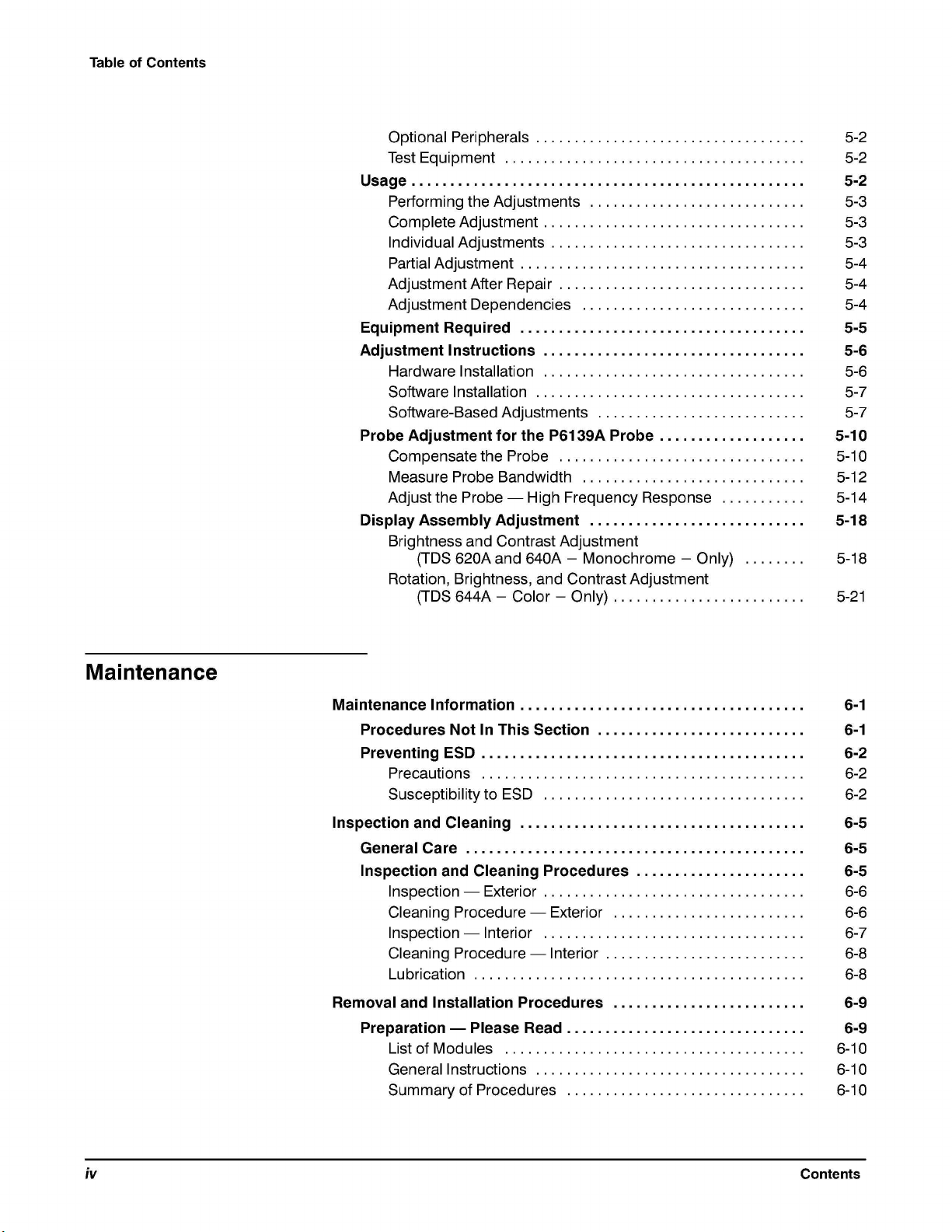
Table of Contents
Optional Peripherals 5-2
Test Equipment 5-2
Usage 5-2
Performing the Adjustments 5-3
Complete Adjustment 5-3
Individual Adjustments 5-3
Partial Adjustment 5-4
Adjustment After Repair 5-4
Adjustment Dependencies 5-4
Equipment Required 5-5
Adjustment Instructions 5-6
Hardware Installation 5-6
Software Installation 5-7
Software-Based Adjustments 5-7
Probe Adjustment for the P6139A Probe 5-10
Compensate the Probe 5-10
Measure Probe Bandwidth 5-12
Adjust the Probe — High Frequency Response 5-14
Display Assembly Adjustment 5-18
Brightness and Contrast Adjustment
(TDS 620A and 640A - Monochrome - Only) 5-18
Rotation, Brightness, and Contrast Adjustment
(TDS 644A - Color - Only) 5-21
Maintenance
Maintenance Information 6-1
Procedures Not In This Section 6-1
Preventing ESD 6-2
Precautions 6-2
Susceptibility to ESD 6-2
Inspection and Cleaning 6-5
General Care 6-5
Inspection and Cleaning Procedures 6-5
Inspection — Exterior 6-6
Cleaning Procedure — Exterior 6-6
Inspection — Interior 6-7
Cleaning Procedure — Interior 6-8
Lubrication 6-8
Removal and Installation Procedures 6-9
Preparation — Please Read 6-9
List of Modules 6-10
General Instructions 6-10
Summary of Procedures 6-10
iv Contents
Page 9
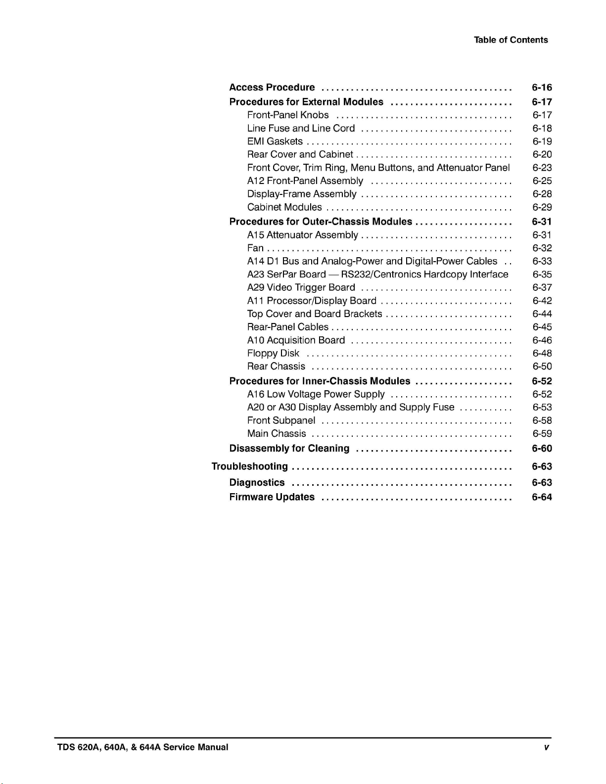
Table of Contents
Access Procedure 6-16
Procedures for External Modules 6-17
Front-Panel Knobs 6-17
Line Fuse and Line Cord 6-18
EMI Gaskets 6-19
Rear Cover and Cabinet 6-20
Front Cover, Trim Ring, Menu Buttons, and Attenuator Panel 6-23
A12 Front-Panel Assembly 6-25
Display-Frame Assembly 6-28
Cabinet Modules 6-29
Procedures for Outer-Chassis Modules 6-31
A15 Attenuator Assembly 6-31
Fan 6-32
A14 D1 Bus and Analog-Power and Digital-Power Cables .. 6-33
A23 SerPar Board — RS232/Centronics Hardcopy Interface 6-35
A29 Video Trigger Board 6-37
A11 Processor/Display Board 6-42
Top Cover and Board Brackets 6-44
Rear-Panel Cables 6-45
A10 Acquisition Board 6-46
Floppy Disk 6-48
Rear Chassis 6-50
Procedures for Inner-Chassis Modules 6-52
A16 Low Voltage Power Supply 6-52
A20 or A30 Display Assembly and Supply Fuse 6-53
Front Subpanel 6-58
Main Chassis 6-59
Disassembly for Cleaning 6-60
Troubleshooting 6-63
Diagnostics 6-63
Firmware Updates 6-64
TDS 620A, 640A, & 644A Service Manual ix
Page 10
Table of Contents
Options
Electrical Parts List
Diagrams
Mechanical Parts List
vi Contents
Page 11
List of Figures
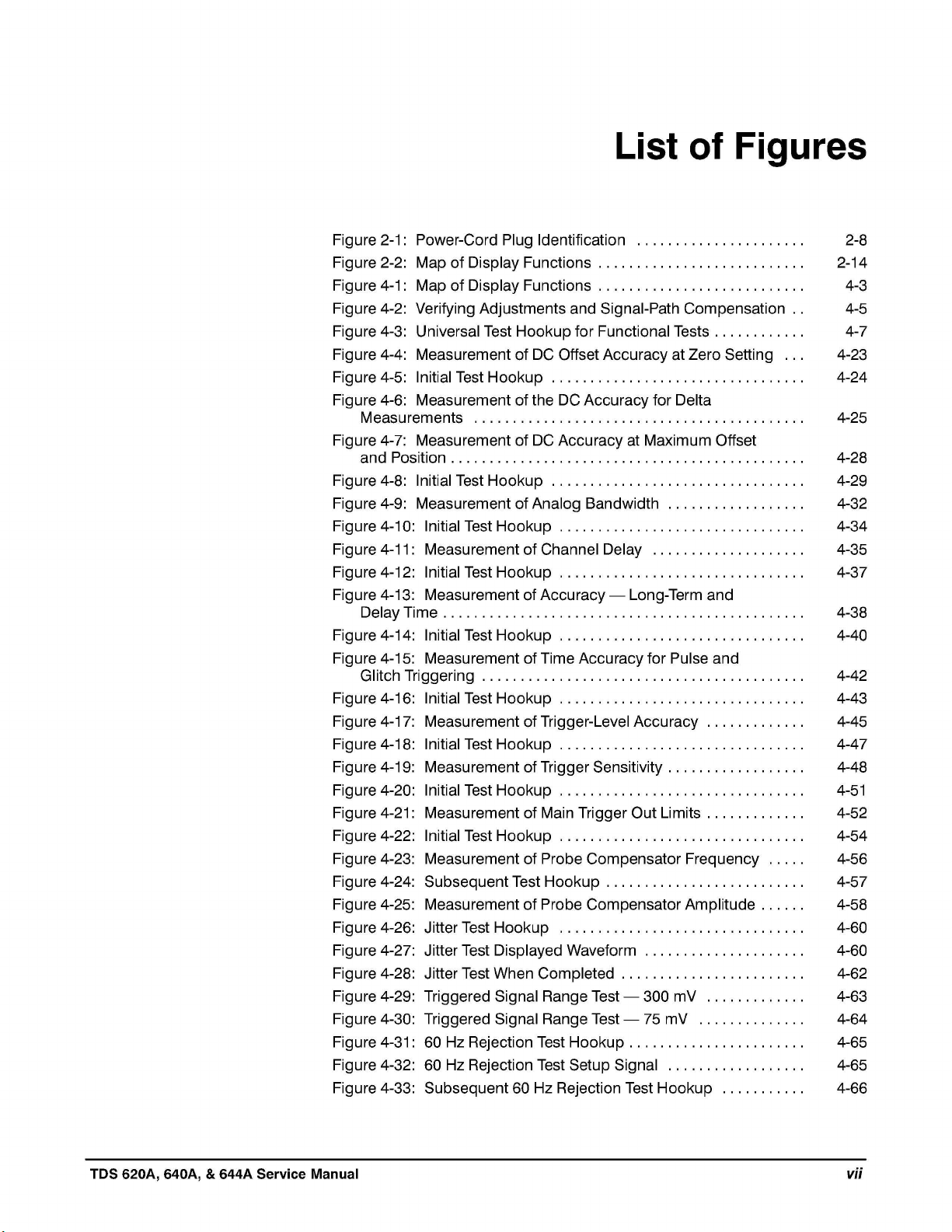
Figure 2-1: Power-Cord Plug Identification 2-8
Figure 2-2: Map of Display Functions 2-14
Figure 4-1: Map of Display Functions 4-3
Figure 4-2: Verifying Adjustments and Signal-Path Compensation .. 4-5
Figure 4-3: Universal Test Hookup for Functional Tests 4-7
Figure 4-4: Measurement of DC Offset Accuracy at Zero Setting ... 4-23
Figure 4-5: Initial Test Hookup 4-24
Figure 4-6: Measurement of the DC Accuracy for Delta
Measurements 4-25
Figure 4-7: Measurement of DC Accuracy at Maximum Offset
and Position 4-28
Figure 4-8: Initial Test Hookup 4-29
Figure 4-9: Measurement of Analog Bandwidth 4-32
Figure 4-10: Initial Test Hookup 4-34
Figure 4-11: Measurement of Channel Delay 4-35
Figure 4-12: Initial Test Hookup 4-37
Figure 4-13: Measurement of Accuracy — Long-Term and
Delay Time 4-38
Figure 4-14: Initial Test Hookup 4-40
Figure 4-15: Measurement of Time Accuracy for Pulse and
Glitch Triggering 4-42
Figure 4-16: Initial Test Hookup 4-43
Figure 4-17: Measurement of Trigger-Level Accuracy 4-45
Figure 4-18: Initial Test Hookup 4-47
Figure 4-19: Measurement of Trigger Sensitivity 4-48
Figure 4-20: Initial Test Hookup 4-51
Figure 4-21: Measurement of Main Trigger Out Limits 4-52
Figure 4-22: Initial Test Hookup 4-54
Figure 4-23: Measurement of Probe Compensator Frequency 4-56
Figure 4-24: Subsequent Test Hookup 4-57
Figure 4-25: Measurement of Probe Compensator Amplitude 4-58
Figure 4-26: Jitter Test Hookup 4-60
Figure 4-27: Jitter Test Displayed Waveform 4-60
Figure 4-28: Jitter Test When Completed 4-62
Figure 4-29: Triggered Signal Range Test — 300 mV 4-63
Figure 4-30: Triggered Signal Range Test — 75 mV 4-64
Figure 4-31: 60 Hz Rejection Test Hookup 4-65
Figure 4-32: 60 Hz Rejection Test Setup Signal 4-65
Figure 4-33: Subsequent 60 Hz Rejection Test Hookup 4-66
TDS 620A, 640A, & 644A Service Manual vii
Page 12
List of Figures
Figure 4-34: 60 Hz Rejection Test Result 4-67
Figure 4-35: Line Count Accuracy Test Hookup 4-68
Figure 4-36: Line Count Accuracy Test Setup Waveform 4-68
Figure 4-37: Line Count Accuracy Correct Result Waveform 4-69
Figure 4-38: PG502 Setup for Sync Duty Cycle Test 4-71
Figure 4-39: Sync Duty Cycle Test: One-Div Neg Pulse Waveform .. 4-72
Figure 4-40: Sync Duty Cycle Test: Critically Adjusted Pulse 4-73
Figure 5-1: Accessing the Protection Switch 5-8
Figure 5-2: Hookup for Probe Compensation 5-10
Figure 5-3: Performing Probe Compensation 5-11
Figure 5-4: Proper and Improper Probe Compensation 5-11
Figure 5-5: Exposing the Inner Probe Tip 5-12
Figure 5-6: Initial Test Hookup 5-12
Figure 5-7: Exposing the Probe Body 5-14
Figure 5-8: Initial Test Hookup 5-15
Figure 5-9: Locations of P6139A Probe Adjustments 5-17
Figure 5-10: Adjustments versus Front-Corner Response 5-17
Figure 5-11: TDS 620A/640A Five and Ten Percent Luminance
Patches 5-19
Figure 5-12: TDS 644A Five and Ten Percent Luminance Patches .. 5-22
Figure 6-1: External Modules 6-12
Figure 6-2: Outer-Chassis Modules 6-13
Figure 6-3: Inner-Chassis Modules - TDS 620A or 640A with
A20 Display Assembly 6-14
Figure 6-4: Inner-Chassis Modules - TDS 644A with A30
Display Assembly 6-15
Figure 6-5: Knob Removal 6-18
Figure 6-6: Line Fuse and Line Cord Removal 6-19
Figure 6-7: Rear Cover and Cabinet Removal 6-22
Figure 6-8: Front Cover, Trim Ring, Menu Buttons, and Attenuator
Panel Removal (Front Cover not Shown) 6-23
Figure 6-9: A12 Front-Panel Assembly Removal 6-26
Figure 6-10: Disassembly of Front-Panel Assembly 6-27
Figure 6-11: Cabinet Modules Removal 6-30
Figure 6-12: Attenuator Interconnect Cable Routing and
Jack Locations 6-32
Figure 6-13: A14 D1 Bus and Analog-Power and Digital-Power
Cables Removal 6-33
Figure 6-14: Remove Circuit Board Assembly From Oscilloscope .. 6-35
Figure 6-15: Remove Circuit Board From Assembly 6-36
Figure 6-16: Circuit Board Installed 6-38
Figure 6-17: Proper Routing of the Video Cable 6-39
Figure 6-18: Circuit Board Removal 6-40
Figure 6-19: A11 Processor/Display Removal 6-43
viii
Contents
Page 13
List of Figures
Figure 6-20: Board Bracket Removal 6-44
Figure 6-21: A10 Acquisition Board Removal 6-47
Figure 6-22: Floppy Disk Removal 6-49
Figure 6-23: Rear Chassis Removal 6-51
Figure 6-24: A16 Low Voltage Power Supply Removal 6-53
Figure 6-25: Display Assembly Removal - TDS 644A 6-55
Figure 6-26: Display Assembly Removal - TDS 620A and 640A ... 6-56
Figure 6-27: Display Driver Board Removal 6-57
Figure 6-28: Front Subpanel Removal 6-59
Figure 6-29: Accessing the Protection Switch 6-64
Figure 6-30: Primary Troubleshooting Procedure 6-65
Figure 6-31: Module Isolation Troubleshooting Procedure 6-67
Figure 6-32: A16 Low Voltage Power Supply Module Isolation
Troubleshooting Procedure 6-68
Figure 6-33: Power Supply Voltage Measurement Locations 6-70
Figure 6-34: Color (TDS 644A) Display Troubleshooting Procedure . 6-71
Figure 6-35: Horizontal and Vertical Sync Signals - Color Display . 6-72
Figure 6-36: A Video Signal with White, Black, and Blanking
Levels - Color Display 6-72
Figure 6-37: Monochrome (TDS 620Aand 640A) Display
Troubleshooting Procedure 6-73
Figure 6-38: Horizontal and Vertical Sync Signals - Monochrome
Display 6-74
Figure 6-39: A Video Signal with White, Black, and Blanking
Levels - Monochrome Display 6-74
Figure 6-40: Processor/Acquisition Troubleshooting Procedure .... 6-75
Figure 6-41: Processor/Front Panel Troubleshooting Procedure .... 6-76
Figure 6-42: Attenuator/Acquisition Troubleshooting Procedure .... 6-77
Figure 6-43: A11 DRAM Processor/Display Module (View of
Right Side) 6-78
Figure 6-44: A11 DRAM Processor/Display Module (View of
Upper Left Corner) 6-79
Figure 6-45: A11 DRAM Processor/Display Module (View of
Lower Left Corner) 6-79
Figure 6-46: A10 Acquisition Module (View of Lower Left Corner) .. 6-80
Figure 9-1: Block Diagram 9-2
Figure 9-2: Interconnections 9-4
Figure 10-1: External Modules 10-5
Figure 10-2: Outer-Chassis Modules 10-7
Figure 10-3: Inner-Chassis Modules - A30 Display Shown 10-9
Figure 10-4: Cables 10-11
Figure 10-5:Floppy Disk 10-13
Figure 10-6: Accessories 10-14
TDS 620A, 640A, & 644A Service Manual ix
Page 14

List of Figures
Contents
Page 15
List of Tables
Table 1-1: Record Length versus Divisions per Record, Samples
per Division, and Sec/Div Sequence 1-3
Table 1-2: Nominal Traits — Signal Acquisition System 1-9
Table1-3: Nominal Traits — Time Base System 1-10
Table1-4: Nominal Traits — Triggering System 1-10
Table1-5: Nominal Traits — Display System 1-11
Table 1-6: Nominal Traits — GPIB Interface, Output Ports, and
Power Fuse 1-11
Table 1-7: Nominal Traits — Mechanical 1-12
Table 1-8: Warranted Characteristics — Signal Acquisition System . 1-13
Table 1-9: Warranted Characteristics — Time Base System 1-14
Table 1-10: Warranted Characteristics — Triggering System 1-15
Table 1-11: Warranted Characteristics — Output Ports, Probe
Compensator, and Power Requirements 1-15
Table 1-12: Warranted Characteristics — Environmental 1-16
Table 1-13: Typical Characteristics — Signal Acquisition System ... 1-19
Table 1-14: Typical Characteristics — Time Base System 1-20
Table 1-15: Typical Characteristics — Triggering System 1-20
Table 1-16: Typical Characteristics — Data Handling and Reliability 1-22
Table 2-1: Power-Cord Conductor Identification 2-8
Table 2-2: Effects of Corrupted Data 2-10
Table 4-1: Test Equipment 4-14
Table 4-2: DC Offset Accuracy (Zero Setting) 4-22
Table 4-3: DC Accuracy 4-27
Table 4-4: Analog Bandwidth 4-30
Table 5-1: Calibration Tests 5-3
Table 5-2: Adjustments Required for Module Replaced 5-4
Table 5-3: Adjustments and Dependencies 5-4
Table 5-4: Test Equipment, Fixtures, and Supplies 5-5
Table 5-5: GPIB Board Configuration 5-7
Table 6-1: Relative Susceptibility to Static-Discharge Damage 6-3
Table 6-2: External Inspection Check List 6-6
Table 6-3: Internal Inspection Check List 6-7
Table 6-4: Tools Required for Module Removal 6-11
Table 6-5: Normal Supply Voltages (Measured on J26 and J27
on the A11 DRAM Processor/Display Module) 6-69
Table 6-6: No-Load Supply Voltages (Measured on J5 and J6
on the A17 Main LV Power Supply Module) 6-69
Table 7-1: International Power Cords 7-1
TDS 620A, 640A, & 644A Service Manual xi
Page 16
List of Tables
Table 7-2: Standard Accessories 7-3
Table 7-3: Optional Accessories 7-4
Table 7-4: Accessory Software 7-5
xii Contents
Page 17
Please take a moment to review these safety precautions. They are provided
for your protection and to prevent damage to the Digitizing Oscilloscopes.
This safety information applies to all operators and service personnel.
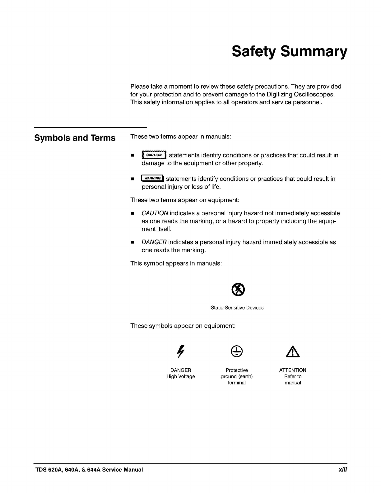
Symbols and Terms These two terms appear in manuals:
caut
• L
• ij««»™^ statements identify conditions or practices that could result in
These two terms appear on equipment:
• CAUTION indicates a personal injury hazard not immediately accessible
!?!L1 statements identify conditions or practices that could result in
damage to the equipment or other property.
personal injury or loss of life.
as one reads the marking, or a hazard to property including the equip-
ment itself.
Safety Summary
• DANGER indicates a personal injury hazard immediately accessible as
one reads the marking.
This symbol appears in manuals:
®
Static-Sensitive Devices
These symbols appear on equipment:
A
DANGER
High Voltage
Protective
ground (earth)
terminal
ATTENTION
Refer to
manual
TDS 620A, 640A, & 644A Service Manual
xiii
Page 18
Safety Summary
Specific Precautions Observe all of the following precautions to ensure your personal safety and
to prevent damage to either the TDS 620A, 640A, & 644A or equipment
connected to it.
Do Not Perform Service While Alone
Do not perform internal service or adjustment of this product unless another
person capable of rendering first aid and resuscitation is present.
Use Care When Servicing With Power On
Dangerous voltages exist at several points in this product. To avoid personal
injury, do not touch exposed connections or components while power is on.
Disconnect power before removing protective panels, soldering, or replacing
components.
Power Source
The TDS 620A, 640A, & 644A is intended to operate from a power source
that will not apply more than 250 VRMs between the supply conductors or
between either supply conductor and ground. A protective ground connec-
tion, through the grounding conductor in the power cord, is essential for safe
system operation.
Grounding the Digitizing Oscilloscopes
The TDS 620A, 640A, & 644A are each grounded through the power cord. To
avoid electric shock, plug the power cord into a properly wired receptacle
where earth ground has been verified by a qualified service person. Do this
before making connections to the input or output terminals of the TDS 620A,
640A, & 644A.
Without the protective ground connection, all parts of the TDS 620A, 640A, &
644A are potential shock hazards. This includes knobs and controls that may
appear to be insulators.
Use the Proper Power Cord
Use only the power cord and connector specified for your product. Use only
a power cord that is in good condition.
Use the Proper Fuse
To avoid fire hazard, use only the fuse specified in the parts list for your
product, and which is identical in type, voltage rating, and current rating.
xiv
Safety
Page 19
Safety Summary
Do Not Remove Covers or Panels
To avoid personal injury, do not operate the TDS 620A, 640A, & 644A without
the panels or covers.
Do Not Operate in Explosive Atmospheres
The TDS 620A, 640A, & 644A provides no explosion protection from static
discharges or arcing components. Do not operate the TDS 620A, 640A, &
644A in an atmosphere of explosive gasses.
Electric Overload
Never apply a voltage to a connector on the TDS 620A, 640A, & 644A that is
outside the range specified for that connector.
TDS 620A, 640A, & 644A Service Manual
XV
Page 20

Safety Summary
xvi Safety
Page 21

Page 22
Specifications
This subsection begins with a general description of the traits of the
TDS 620A, 640A, & 644A Digitizing Oscilloscopes. Three subsections follow,
one for each of three classes of traits: nominal traits, warranted characteris-
tics, and typical characteristics.
General Product The TDS 620A, 640A, & 644A are portable, four-channel digitizing oscillo-
Description scopes suitable for use in a variety of test and measurement applications
p
and systems. Key features include:
• A maximum digitizing rate of 2 GS/s on each of the full-featured chan-
nels (four on the TDS 640A and 644A, two on the TDS 620A) simulta-
neously with an analog bandwidth of 500 MHz.
• Four input channels, each with 8-bit vertical resolution, and each with a
record length of 2,000 samples and 8-bit vertical resolution.
• Extensive triggering capabilities: such as edge, logic, and glitch. Video
trigger (Option 05) is also available. The video trigger modes are NTSC,
SECAM, PAL, HDTV, and FlexFormat™ (user definable format).
• Acquisition modes such as sample, envelope, and average.
• A full complement of advanced functions, like continuously-updated
measurements, results and local pass/fail decision making.
• Specialized display modes, such as variable persistence with color
grading, dot or vector mode, sin(x)/x or linear display filters, and user
selectable color pallettes. The "Fit to Screen" features compresses the
entire waveform record to fit on the screen.
• A unique graphical user interface (GUI), an on-board help mode, and a
logical front-panel layout which combine to deliver a new standard in
usability.
• Full GPIB software programmability. Hardcopy output using GPIB,
RS-232, or Centronics ports. RS-232 and Centronics are standard on
the TDS 644A and optional, as option 13, on the TDS 620A and 640A.
• VGA output for driving remote monitors.
• A 1.44 Mbyte, DOS 3.3 or later-compatible, floppy disk drive (option 1F
on the TDS 620A and 640A) and NVRAM mass storage for saving
waveforms, hardcopies, and oscilloscope setups.
• On the TDS 644A, a color display for distinguishing among waveforms,
their measurements, and associated text.
TDS 620A, 640A, & 644A Service Manual
1-1
Page 23
Specifications
User Interface Use a combination of front-panel buttons, knobs, and on-screen menus to
control the oscilloscope's many functions. The front-panel controls are
grouped according to function: vertical, horizontal, trigger, and special. Set a
function you adjust often, such as vertical positioning or the time base
setting, directly by its own front-panel knob. Set functions which you change
less often, such as vertical coupling and horizontal mode, indirectly using
selected menus.
Menus
Pressing one (sometimes two) front-panel button(s), such as vertical menu,
displays a main menu of related functions, such as coupling, bandwidth,
etc., at the bottom of the screen. Pressing a main-menu button, such as
coupling, displays a side menu of settings for that function, such as AC, DC,
or GND (ground) coupling, at the right side of the screen. Pressing a side-
menu button selects a setting such as DC.
Indicators
On-screen readouts help you keep track of the settings for various functions,
such as vertical and horizontal scale and trigger level. Some readouts use
the cursors or the automatic parameter extraction feature (called measure)
to display the results of measurements made or the status of the instrument.
General Purpose Knob
Assign the general purpose knob to adjust a selected parameter function.
More quickly change parameters by toggling the SHIFT button. Use the
same method as for selecting a function, except the final side-menu selec-
tion assigns the general purpose knob to adjust some function, such as the
position of measurement cursors on screen, or the setting for a channel's
fine gain.
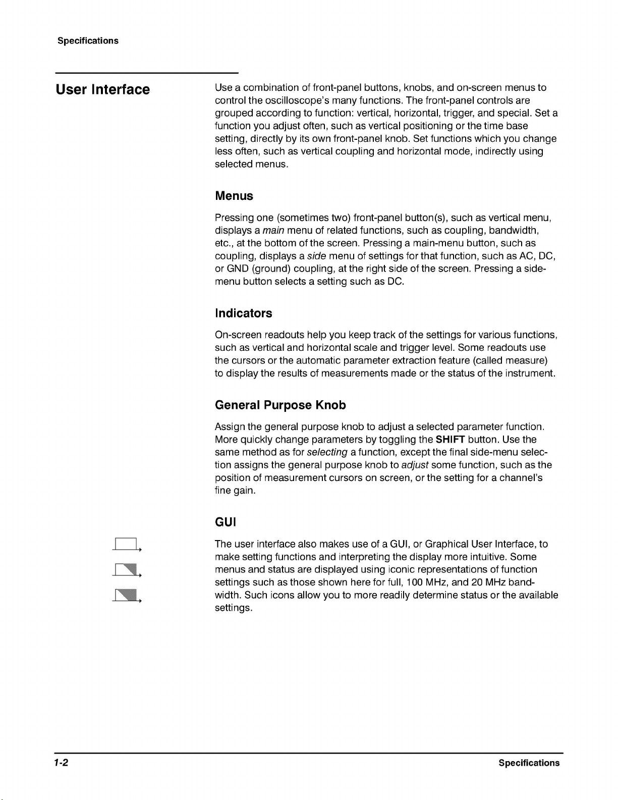
GUI
I ^ The user interface also makes use of a GUI, or Graphical User Interface, to
make setting functions and interpreting the display more intuitive. Some
J
< menus and status are displayed using iconic representations of function
settings such as those shown here for full, 100 MHz, and 20 MHz band-
J \ width. Such icons allow you to more readily determine status or the available
settings.
7-2
Specifications
Page 24
Specifications
Signal Acquisition
Svstem
The signal acquisition system provides full-featured vertical channels (four
on the TDS 640A and 644A, two on the TDS 620A) with calibrated vertical
scale factors from 1 mV to 10 V per division. All four channels can be ac-
quired simultaneously.
Each of the four channels can be displayed, vertically positioned, and offset,
can have their bandwidth limited (100 MHz or 20 MHz) and their vertical
coupling specified. Fine gain can also be adjusted.
Besides these channels, up to three math waveforms and four reference
waveforms are available for display. (A math waveform results when you
specify dual waveform operations, such as add, on any two channels. A
reference waveform results when you save a live waveform in a reference
memory.)
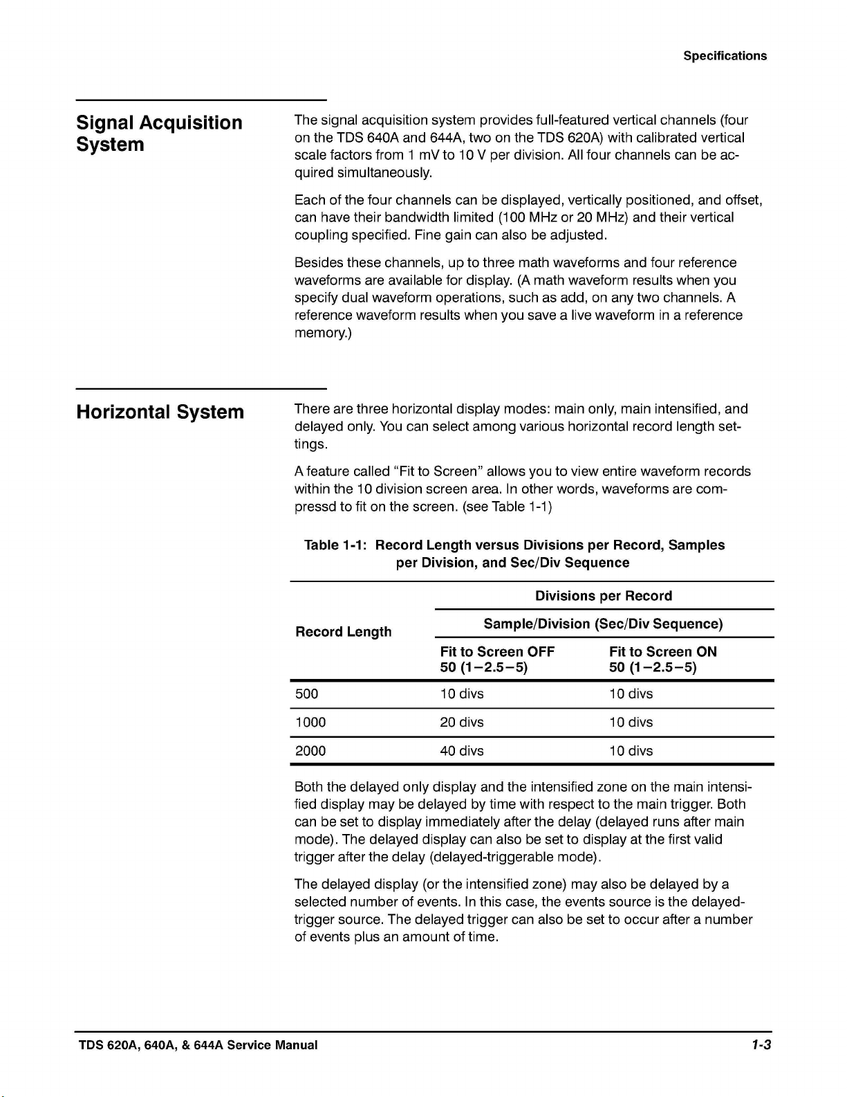
Horizontal Svstem There are three horizontal display modes: main only, main intensified, and
delayed only. You can select among various horizontal record length set-
tings.
A feature called "Fit to Screen" allows you to view entire waveform records
within the 10 division screen area. In other words, waveforms are com-
pressd to fit on the screen. (see Table 1-1)
Table 1-1: Record Length versus Divisions per Record, Samples
per Division, and Sec/Div Sequence
Divisions per Record
Record Length
Record Length
Fit to Screen OFF Fit to Screen ON
50 (1-2.5-5) 50 (1-2.5-5)
500 10 divs 10 divs
1000 20 divs 10 divs
2000 40divs 10divs
Both the delayed only display and the intensified zone on the main intensi-
fied display may be delayed by time with respect to the main trigger. Both
can be set to display immediately after the delay (delayed runs after main
mode). The delayed display can also be set to display at the first valid
trigger after the delay (delayed-triggerable mode).
The delayed display (or the intensified zone) may also be delayed by a
selected number of events. In this case, the events source is the delayed-
trigger source. The delayed trigger can also be set to occur after a number
of events plus an amount of time.
Sample/Division (Sec/Div Sequence)
TDS 620A, 640A, & 644A Service Manual 1-3
Page 25
Specifications
Trigger System The triggering system supports a varied set of features for triggering the
signal-acquisition system. Trigger signals recognized include:
• Edge (main- and delayed-trigger systems): This familiar type of trigger-
ing is fully configurable for source, slope, coupling, mode (auto or
normal), and holdoff.
• Logic (main-trigger system): This type of triggering can be based on
pattern (asynchronous) or state (synchronous). In either case, logic
triggering is configurable for sources, for boolean operators to apply to
those sources, for logic pattern or state on which to trigger, for mode
(auto or normal), and for holdoff. Time qualification may be selected in
pattern mode.
• Pulse (main-trigger system): Pulse triggering is configurable for trigger-
ing on runt or glitch pulses, or on pulse widths or periods inside or
outside limits that you specify. It is also configurable for source, polarity,
mode, and holdoff.
• Video (with option 05: Video Trigger): Video triggering is compatible with
standard NTSC, PAL, SECAM, and HDTV formats. An additional feature
called FlexFormat™ (flexible format) allows the user to define the video
format on which to trigger.
You can choose where the trigger point is located within the acquired wave-
form record by selecting the amount of pretrigger data displayed. Presets of
20%, 50%, and 80% of pretrigger data can be selected in the horizontal
menu, or the general purpose knob can be assigned to set pretrigger data
to any value within the 20% to 80% limits.
Acquisition Control You can specify a mode and manner to acquire and process signals that
matches your measurement requirements.
• Select the mode for interpolation of points sampled on non-repetitive
signals (linear or sin (x)/x. This can increase the apparent sample rate
on the waveform when maximum real-time rates are reached.
• Use sample, envelope, and average modes to acquire signals.
• Set the acquisition to stop after a single acquisition (or sequence of
acquisitions if acquiring in average or envelope modes), or after a limit
condition has been met.
• Select channel sources for compliance with limit tests. You can direct
the TDS to signal you or generate hard copy output either to a printer or
to a floppy disk (with option 1F) based on the results. Also, you can
create templates for use in limit tests.
7-4 Specifications
Page 26
Specifications
On-Board User Help and autoset
can
assist you in setting up the Digitizing Oscilloscope to
Assistance make your measurements.
Help
Help displays operational information about any front-panel control. When
help mode is in effect, manipulating any front-panel control causes the
Digitizing Oscilloscope to display information about that control. When help
is first invoked, an introduction to help is displayed on screen.
Autoset
Autoset automatically sets up the Digitizing Oscilloscope for a viewable
display based on the input signal.
Measurement Once you have set up to make your measurements, the cursor and measure
Assistance features can help you quickly make those measurements.
Cursor
Three types of cursors are provided for making parametric measurements
on the displayed waveforms. Horizontal bar cursors (H Bar) measure vertical
parameters (typically volts). Vertical bar cursors (V Bar) measure horizontal
parameters (typically time or frequency) and now extend to the top and
bottom of the screen. Paired cursors measure both amplitude and time
simultaneously. These are delta measurements; that is, measurements
based on the difference between two cursors.
Both H Bar and V Bar cursors can also be used to make absolute measure-
ments; that is measurements relative to a defined level or event. For the
H Bars, either cursor can be selected to read out its voltage with respect to
any channels ground reference level. For the V Bars, it's time with respect to
the trigger point (event) of the acquisition and the cursors can control the
portion of the waveform on which automatic measurements are made.
For time measurements, units can be either seconds or Hertz (for 1/time).
When the video trigger option installed (Option 05), you can measure the
video line number using the vertical cursors. You can measure IRE ampli-
tude (NTSC) using the horizontal cursors with or without the video trigger
option installed.
Measure
Measure can automatically extract parameters from the signal input to the
Digitizing Oscilloscope. Any four out of the more than 25 parameters avail-
able can be displayed to the screen. The waveform parameters are mea-
sured continuously with the results updated on-screen as the Digitizing
Oscilloscope continues to acquire waveforms.
TDS 620A, 640A, & 644A Service Manual 1-5
Page 27
Specifications
Digital Signal Processing (DSP)
An important component of the multiprocessor architecture of this Digitizing
Oscilloscope is Tektronix's proprietary digital signal processor, the DSF! This
dedicated processor supports advanced analysis of your waveforms when
doing such compute-intensive tasks as interpolation, waveform math, and
signal averaging. It also teams with a custom display system to deliver
specialized display modes (See Display, later in this description.)
and I/O Acquired waveforms may be saved in any of four nonvolatile REF (reference)
memories or on a 3.5 inch, DOS 3.3-or-later compatible disk. Any or all of
the saved waveforms may be displayed for comparison with the waveforms
being currently acquired.
The source and destination of waveforms to be saved may be chosen. You
can save any of the four channels to any REF memory or to move a stored
reference from one REF memory to another. Reference waveforms may also
be written into a REF memory location via the GFIB interface.
The Digitizing Oscilloscope is fully controllable and capable of sending and
receiving waveforms over the GFIB interface (IEEE Std 488.1-1987/IEEE
Std 488.2-1987 standard). This feature makes the instrument ideal for
making automated measurements in a production or research and develop-
ment environment that calls for repetitive data taking. Self-compensation
and self-diagnostic features built into the Digitizing Oscilloscope to aid in
fault detection and servicing are also accessible using commands sent from
a GFIB controller.
Another standard feature is hardcopy. This feature allows you to output
waveforms and other on-screen information to a variety of graphic printers
and plotters from the TDS front panel, providing hard copies without requir-
ing you to put the TDS into a system-controller environment. You can make
hardcopies in a variety of popular output formats, such as FCX, TIFF, BMF!
RLE, EFS, Interleaf, and EFS mono or color. You can also save hardcopies
in a disk file in any of the formats above. The hardcopies obtained are based
on what is displayed on-screen at the time hardcopy is invoked. The hardco-
pies can be stamped with date and time and spooled to a queue for printing
at a later time. You can output screen information via GFIB, RS-232C, or
Centronics interfaces.
7-6 Specifications
Page 28
Specifications
Display
The TDS 620A, 640A, & 644A Digitizing Oscilloscopes offers flexible display
options. You can customize the following attributes of your display:
Color (on the TDS 644A): waveforms, readouts, graticule, and variable
persistence with color coding;
Intensity: waveforms, readouts, and graticule;
Style of waveform display(s): vectors or dots, intensified or non-intensi-
fied samples, infinite persistence, and variable persistence with color
coding;
Interpolation method: Sin(x)/x or Linear;
Display format: xy or yt with various graticule selections including NTSC
and PAL to be used with video trigger (option 05).
Zoom
This oscilloscope also provides an easy way to focus in on those waveform
features you wish to examine up close. By invoking zoom, you can magnify
the waveform parameter using the vertical and horizontal controls to expand
(or contract) and position it for viewing.
TDS 620A, 640A, & 644A Service Manual
1-7
Page 29

Specifications
7-8 Specifications
Page 30
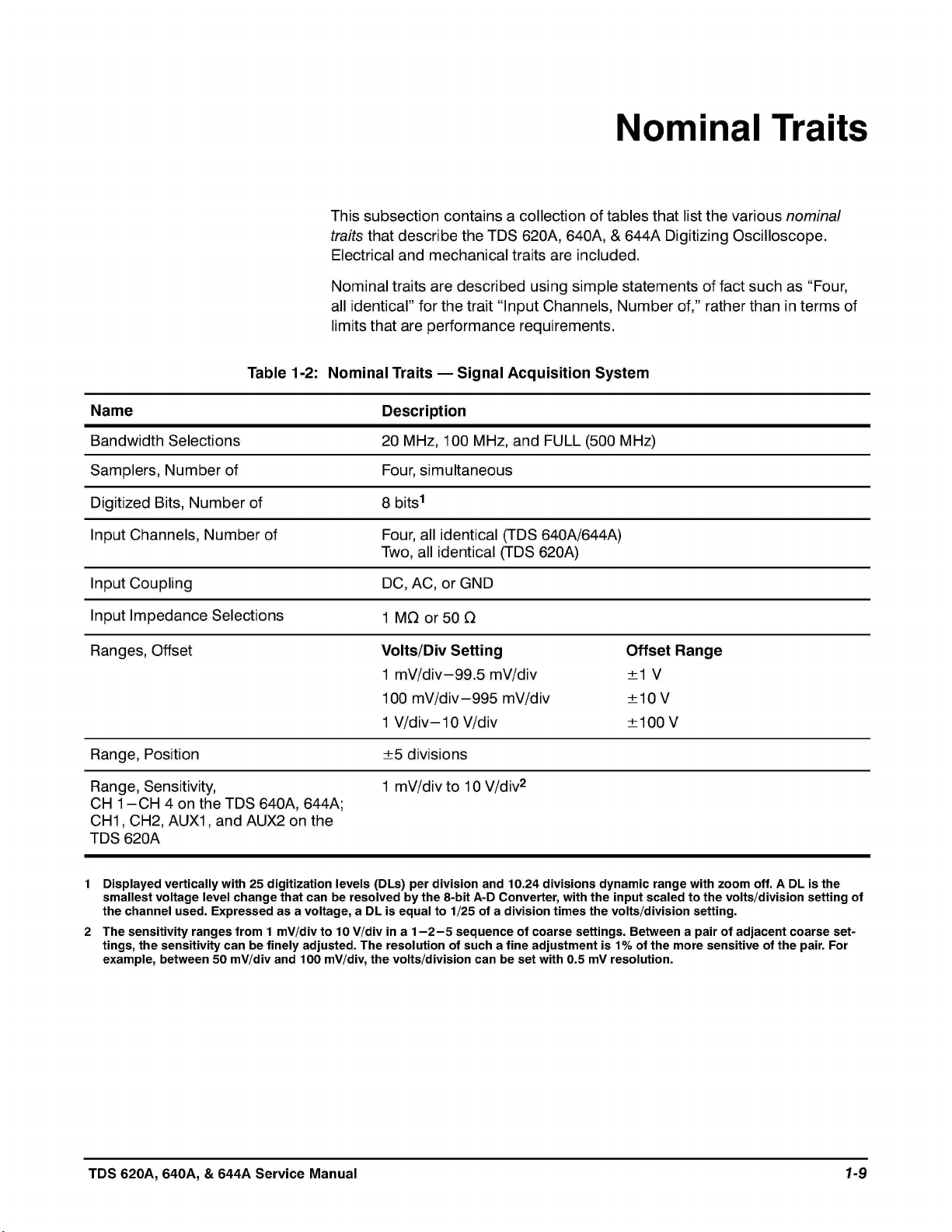
Nominal Traits
This subsection contains a collection of tables that list the various nominal
traits that describe the TDS 620A, 640A, & 644A Digitizing Oscilloscope.
Electrical and mechanical traits are included.
Nominal traits are described using simple statements of fact such as "Four,
all identical" for the trait "Input Channels, Number of," rather than in terms of
limits that are performance requirements.
Table 1-2: Nominal Traits — Signal Acquisition System
Name
Bandwidth Selections
Samplers, Number of Four, simultaneous
Digitized Bits, Number of
Input Channels, Number of Four, all identical (TDS 640A/644A)
Input Coupling
Input Impedance Selections
Ranges, Offset
Range, Position ±5 divisions
Range, Sensitivity,
CH 1-CH 4 on the TDS 640A, 644A;
CH1, CH2, AUX1, and AUX2 on the
TDS 620A
Description
20 MHz, 100 MHz, and FULL (500 MHz)
1
8 bits
Two, all identical (TDS 620A)
DC, AC, or GND
1 MO or 50 O
Volts/Div Setting Offset Range
1 mV/div-99.5 mV/div ±1 V
100 mV/div-995 mV/div
1 V/div-10 V/div ±100 V
1 mV/div to 10 V/div
2
±10 V
1 Displayed vertically with 25 digitization levels (DLs) per division and 10.24 divisions dynamic range with zoom off. A DL is the
smallest voltage level change that can be resolved by the 8-bit A-D Converter, with the input scaled to the volts/division setting of
the channel used. Expressed as a voltage, a DL is equal to 1/25 of a division times the volts/division setting.
2 The sensitivity ranges from 1 mV/div to 10 V/div in a 1-2-5 sequence of coarse settings. Between a pair of adjacent coarse set-
tings, the sensitivity can be finely adjusted. The resolution of such a fine adjustment is 1% of the more sensitive of the pair. For
example, between 5o mV/div and 1o0 mV/div, the volts/division can be set with 0.5 mV resolution.
TDS 620A, 640A, & 644A Service Manual 1-9
Page 31

Nominal Traits
Table 1-3: Nominal Traits — Time Base System
Name Description
Range, Sample-Rate1'
3
10 Samples/sec to 2 GSamples/sec on four (TDS 640A/644A) or two
(TDS 620A) channels simultaneously.
Range, Interpolated Waveform Rate2,
3
5 GSamples/sec to 100 GSamples/sec
(200 ps/Sample to 10 ps/Sample)
Range, Seconds/Division 500 ps/div to 5 s/div
Record Length Selection 500 samples, 1000 samples, 2000 samples.
1 The range of real-time rates, expressed in samples/second, at which a digitizer samples signals at its inputs and stores the sam-
ples in memory to produce a record of time-sequential samples.
2 The range of waveform rates for interpolated waveform records.
3 The Waveform Rate (WR) is the equivalent sample rate of a waveform record. For a waveform record acquired by real-time sam-
pling of a single acquisition, the waveform rate is the same as the real-time sample rate; for a waveform created by interpolation of
real-time samples from a single acquisition, the waveform rate is faster than the real time sample rate. For both cases, the wave-
form rate is 1/(Waveform Interval) for the waveform record, where the waveform interval (Wl) is the time between the samples in the
waveform record.
Table 1-4: Nominal Traits — Triggering System
Name Description
Range, Delayed Trigger Time Delay 16 ns to 250 s
Range, Events Delay 2 to 10,000,000
Range (Time) for Pulse-Glitch or Pulse-
2 ns to 1 s
Width Triggering
Ranges, Trigger Level or Threshold Source Range
Any Channel ±12 divisions from center of screen
Auxiliary ±8 V
Line ±300 V
Video Trigger Modes of Operation
(Option 05 Video Trigger)
Supports the following video standards:
• NTSC (525/60) - 2 field mono or 8 field
• PAL (625/50) - 2 field mono, 8 field, or SECAM
• HDTV -
(787.5/60)
(1050.60)
(1125/60)
(1250/60)
• FlexFormat™ (user definable standards)
User can specify: field rate, number of lines, sync pulse width
and polarity, line rate, and vertical interval timing.
1-10 Specifications
Page 32

Table 1-5: Nominal Traits — Display System
Name Description
Nominal Traits
Video Display
Color (on the TDS 644A) or monochrome (on the TDS 620A, 640A)
display, 7 inch diagonal, with a display area of 5.04 inches horizon-
tally by 3.78 inches vertically
Video Display Resolution 640 pixels horizontally by 480 pixels vertically
Waveform Display Graticule
Single Graticule: 401 x 501 pixels, 8 x10 divisions, where divisions
are 1 cm by 1 cm
Waveform Display Colors Scale
TDS 644A: Sixteen colors in infinite-persistence or variable persis-
tence display with color coding.
TDS 620Aand 640A: Sixteen levels in infinite-persistence or varia-
ble-persistence display styles.
Table 1-6: Nominal Traits — GPIB Interface, Output Ports, and Power Fuse
Name Description
Interface, GPIB
Interface, RS-232
Interface, Centronics
GPIB interface complies with IEEE Std 488-1987
RS-232 interface complies with EIA/TIA 574 (talk only)
Centronics interface complies with Centronics interface standard
C332-44 Feb 1977, REV A
Interface, Video
VGA video output with levels that comply with ANSI R5343A stan-
dard. DB-15 connector.
Logic Polarity for Main- and Delayed- Negative TRUE. High to low transition indicates the trigger occurred.
Trigger Outputs
Fuse Rating Either of two fuses1 maybe used: a .25" x 1.25" (UL 198.6, 3AG):
6 A FAST, 250 V, or a 5 mm x 20 mm, (IEC 127): 5 A (T), 250 V.
1 Each fuse type requires its own fuse cap.
TDS 620A, 640A, & 644A Service Manual
1-11
Page 33

Nominal Traits
Table 1-7: Nominal Traits — Mechanical
Name Description
Cooling Method Forced-air circulation with no air filter
Construction Material Chassis parts constructed of aluminum alloy; front panel con-
structed of plastic laminate; circuit boards constructed of glass lami-
nate. Cabinet is aluminum and is clad in Tektronix Blue vinyl materi-
al.
Finish Type Tektronix Blue vinyl-clad aluminum cabinet
Weight Standard TDS 644A Digitizing Oscilloscope
13.7 kg (30 lbs), with front cover.
25.1 kg (55 lbs), when packaged for domestic shipment.
Standard TDS 620A and 640A Digitizing Oscilloscope
12.3 kg (29 lbs), with front cover.
20.0 kg (44 lbs), when packaged for domestic shipment.
RackmountTDS 644A Digitizing Oscilloscope
13.7 kg (30 lbs) plus weight of rackmount parts, for the rack-
mounted Digitizing Oscilloscope (Option 1R).
Rackmount TDS 620A and 640A Digitizing Oscilloscope
12.3 kg (27 lbs) plus weight of rackmount parts, for the rack-
mounted Digitizing Oscilloscope (Option 1R).
Rackmount conversion kit
2.3 kg (5 lbs), for the rackmount conversion kit only; 3.6 kg
(8 lbs), when the kit is packaged for domestic shipping.
Overall Dimensions Standard Digitizing Oscilloscope
Height: 193 mm (7.6 in), with the feet installed.
Width: 445 mm (17.5 in), with the handle.
Depth: 434 mm (17.1 in), with the front cover installed.
Rackmount Digitizing Oscilloscope
Height: 178 mm (7.0 in).
Width: 483 mm (19.0 in).
Depth: 558.8 mm (22.0 in).
1-33
Specifications
Page 34

Warranted Characteristics
This subsection lists the various warranted characteristics that describe the
TDS 620A, 640A, & 644A Digitizing Oscilloscopes. Electrical and
environmental characteristics are included.
Warranted characteristics are described in terms of quantifiable performance
limits which are warranted.
NOTE
In these tables, those warranted characteristics that are checked in
the procedure Performance Verification, found in Section 1, appear
in boldface type under the column Name.
As stated above, this subsection lists only warranted characteristics. A list of
typical characteristics starts on page 1-19.
Performance
Conditions
Table 1-8: Warranted Characteristics — Signal Acquisition System
Name Description
Accuracy, DC Gain
Accuracy, Offset
1
1
The electrical characteristics found in these tables of warranted characteris-
tics apply when the oscilloscope has been adjusted at an ambient tempera-
ture between +20° C and +30° C, has had a warm-up period of at least 20
minutes, and is operating at an ambient temperature between 0° C and
+50° C (unless otherwise noted).
±1.5%.
(For all sensitivities from 2 mV/div to 10 V/div and offsets from 0 to
±100 V)
At 1 mV/div ± 2.0%
Volts/Div Setting
1 mV/div - 99.5 mV/div ±(0.2% x Net Offset
100 mV/div - 995 mV/div ±(0.35% x Net Offset
1 V/div - 10 V/div
Offset Accuracy
+ 1.5 mV + 0.6 div)
+ 15mV + 0.6 div)
±(0.35% x Net Offset
+ 150 mV + 0.6 div)
2
2
2
TDS 620A, 640A, & 644A Service Manual 1-13
Page 35

Warranted Characteristics
Table 1-8: Warranted Characteristics — Signal Acquisition System (Cont.)
Name
Analog Bandwidth, DC-50 O
Coupled, or DC-1 MO Coupled with
P6139A Probe
Description
Volts/Div Bandwidth
3
5 mV/div - 10 V/div DC - 500 MHz
2 mV/div - 4.98 mV/div DC - 300 MHz
1 mV/div - 1.99 mV/div DC - 200 MHz
Cross Talk (Channel Isolation) >100:1 at 100 MHz and >30:1 at the rated bandwidth for the chan-
nel's sensitivity rating, for any two channels having equal volts/divi-
sion settings
Input Impedance, DC-1 MO Coupled 1 MO ±0.5% in parallel with 10 pF ±2 pF
Input Impedance, DC-50 O Coupled
Input Voltage, Maximum, DC-1 MO,
50 O ±1% with VSWR < 1.3:1 from DC - 500 MHz
±400 V (DC + peak AC); derate at 20 dB/decade above 1 MHz
AC-1 MO, or GND Coupled
Input Voltage, Maximum, DC-50 O or
5 V
, with peaks less than or equal to ±30 V
RMS
AC-50 O Coupled
Lower Frequency Limit, AC Coupled
1 To ensure the most accurate measurements possible, run an SPC calibration first. When using the Digitizing Oscilloscope at a
Volts/Div setting of <5 mV/div, an SPC calibration should be run once per week to ensure that instrument performance levels meet
specifications.
2 Net Offset = Offset - (Position x Volts/Div). Net Offset is the voltage level at the center of the A-D converter's dynamic range. Offset
Accuracy is the accuracy of this Voltage level.
3 The limits given are for the ambient temperature range of 0°C to +30°C. Reduce the upper bandwidth frequencies by 2.5 MHz for
each °C above +30°C.
4 The AC Coupled Lower Frequency Limits are reduced by a factor of 10, when 10X passive probes are used.
<10 Hz when AC-1 MO Coupled; <200 kHz when AC-50 O
Coupled
4
Table 1-9: Warranted Characteristics — Time Base System
Name Description
Accuracy, Long Term Sample Rate ±100 ppm over any > 1 ms interval
and Delay Time
1-14
Specifications
Page 36

Table 1-10: Warranted Characteristics — Triggering System
Warranted Characteristics
Name
Accuracy (Time) for Pulse-Glitch or
Pulse-Width Triggering
Sensitivity, Edge-Type Trigger, DC
Coupled
1
Description
Time Range
2 ns to 1 |is
1.02 |is to 1 s
Trigger Source
Accuracy
±(20% x | Setting | + 0.5 ns)
±(100 ns + 0.01% x | Setting | )
Sensitivity
Any Channel 0.35 division from DC to 50 MHz, increasing to
1 division at 500 MHz
0.25 volts from DC to 50 MHz
Minimum
Minimum Rearm Width
Pulse Width
2 ns
2 ns + 5% of Glitch Width
Width, Minimum Pulse and Rearm, for
Pulse Triggering
Auxiliary
Pulse Class
Glitch
Setting
Runt
Width
2.5 ns
2 ns
2.5 ns
2 ns + 5% of Width Upper Limit
Setting
Jitter (Option 05 Video Trigger) 17 nsp_p on HDTV signal; 60 nsp_p on NTSC or PAL signal
Input Signal Sync Amplitude for 0.6 division to 4 divisions with (1 to 4 divisions in numeric field)
Stable Triggering (Option 05 Video
Trigger)
1 The minimum sensitivity for obtaining a stable trigger. A stable trigger results in a uniform, regular display triggered on the se-
lected slope. The trigger point must not switch between opposite slopes on the waveform, and the display must not "roll" across
the screen on successive acquisitions. The TRIG'D LED stays constantly lighted when the SEC/DIV setting is 2 ms or faster but
may flash when the SEC/DIV setting is 10 ms or slower.
Table 1-11: Warranted Characteristics — Output Ports, Probe Compensator, and
Power Requirements
Name Description
Logic Levels, Main- and Delayed-
Trigger Outputs
Characteristic Limits
Vout (HI)
>2.5 V open circuit; > 1.0 V into a 50 O load to
ground
Vout (LO)
Vout (LO)
< 0.7 V into a load of <4 mA; < 0.25 V into a
50 O load to ground
Output Voltage and Frequency, Characteristic Limits
Probe Compensator
Output Voltage, Signal Out (CH 31)
Voltage 0.5 V (base-top) ±1% into a load of >50 O
Frequency
1 kHz ±5%
20 mV/division ±20% into a 1 MO load; 10 mV/division ±20% into a
50 O load
Source Voltage 90 to 250 VAC
, continuous range
RMS
Source Frequency 47 Hz to 63 Hz
TDS 620A, 640A, & 644A Service Manual 1-15
Page 37

Warranted Characteristics
Table 1-11: Warranted Characteristics — Output Ports, Probe Compensator, and
Power Requirements (Cont.)
Name
Description
Power Consumption <300 W (450 VA)
1 CH 3 signal out is only present at the rear panel if CH 3 is selected as the trigger source for the main and/or delayed trigger sys-
tems.
Table 1-12: Warranted Characteristics — Environmental
Name Description
Atmospherics Temperature with floppy disk:
Operating: +4° Cto +50° C;
Non-operating: -22° Cto +60° C
Temperature without floppy disk:
Operating: 0° Cto +50° C;
Non-operating: -40° Cto +60° C
Relative humidity with floppy disk:
Operating: To 80%, at or below +29° C;
Operating: To 20%, at or below +50° C
Non-operating: To 90%, at or below +40° C;
Non-operating: To 5%, at or below +50° C
Relative humidity without floppy disk:
To 95%, at or below +40° C;
To 75%, from +41 ° C to +55° C
Altitude:
To 4570 m (15,000 ft.), operating;
To 12190 m (40,000 ft.), non-operating
Dynamics
Random vibration without floppy disk installed:
0.31 g rms, from 5 to 500 Hz, 10 minutes each axis, operating;
3.07 g rms, from 5 to 500 Hz, 10 minutes each axis, non-operat-
ing
Emissions Meets or exceeds the requirements of the following standards:
Vfg. 243/1991 Amended per Vfg. 46/1992
FCC Code of Federal Regulations, 47 CFR, Part 15, Subpart B,
Class A
User-Misuse Simulation Electrostatic Discharge Susceptibility: Up to 8 kV with no change to
control settings or impairment of normal operation; up to 15 kVwith
no damage that prevents recovery of normal operation
1-16 Specifications
Page 38

Table 1-12: Warranted Characteristics — Environmental (Cont.)
Warranted Characteristics
Name
Description
Third Party Certification Conforms to and is certified where appropriate to:
UL1244
CSA-C22 No. 231
TDS 620A, 640A, & 644A Service Manual
1-17
Page 39

Warranted Characteristics
1-18 Specifications
Page 40

Typical Characteristics
This subsection contains tables that list the various typical characteristics
which describe TDS 620A, 640A, & 644A Digitizing Oscilloscope.
Typical characteristics are described in terms of typical or average
performance. Typical characteristics are not warranted.
Table 1-13: Typical Characteristics — Signal Acquisition System
Name Description
Accuracy, Delta Time Measurement For single-shot acquisitions using single-shoot sample acquisition
Frequency Limit, Upper, 100 MHz
Bandwidth Limited
Frequency Limit, Upper, 20 MHz
Bandwidth Limited
Calculated Rise Time
2
1
mode.
Time Measurement Error < .15 x Si + (100 ppm x |Reading|) + (Time
Per Div ^ 1000)
Add 50 ps (typical) Channel Skew for 2 channel measurements.
Sample calculation:
To measure the width of a 65.5 ns pulse at 2 GS/sec sampling,
Time Measurement Error
< (0.15 x 0.5 ns) + (1 x 10⁻⁴)(65.5 ns) + (25 ns/div. ^ 1000)
< 0.075 ns + 0.007 ns + 0.025 ns
< 107 ps
100 MHz
20 MHz
Volts/Div Setting
5 mV/div - 10 V/div 800 ps
2 mV/div - 4.98 mV/div
1 mV/div - 1.99 mV/div
Rise Time
1.3 ns
2.0 ns
Delay Between Channels, Full
Bandwidth
Step Response Settling Errors
1 The limits are given for signals having pulse height > 5 div, reference level = 50% mid-point, filter set to Sin (x) /x acquired at
>5 mV/div, 1.4 <
TDS 620A, 640A, & 644A Service Manual 1-19
Tr
,Si < 5, where Si is the hardware sample interval and tr is the signal rise time.
<50 ps for any two channels with equal volts/division and coupling
settings
Volts/Div Setting
1 mV/div - 99.5 mV/div <2 V <0.5 <0.2 <0.1
100 mV/div - 995 mV/div
1 V/div - 10 V/div <200 V <1.0 <0.5 <0.2
± Step Settling Error (%)3 at
Response
20 ns 100 ns 20 ms
<20 V <1.0 <0.5 <0.2
Page 41

Typical Characteristics
The numbers given are valid 0°C to +30°C and will increase as the temperature increases due to the degradation in bandwidth.
Rise time is calculated from the bandwidth. It is defined by the following formula:
Rise Time (ns) =
Note that if you measure rise time, you must take into account the rise time of the test equipment (signal source, etc.) that you use
to provide the test signal. That is, the measured risetime (RTm) is determined by the instrument risetime (RTi) and the risetime of
the test signal source (RTgen) according to the following formula:
RTm 2 = RTi 2 + RT
The values given are the maximum absolute difference between the value at the end of a specified time interval after the mid-level
crossing of the step, and the value one second after the mid-level crossing of the step, expressed as a percentage of the step am-
plitude.
400
BW (MHz)
2
gen
Table 1-14: Typical Characteristics — Time Base System
Name Description
Aperture Uncertainty <5 ps @ <250 ns/div
<50 ps @ >500 ns/div
Table 1-15: Typical Characteristics —
Triggering System
Name Description
Accuracy, Trigger Level or Threshold,
DC Coupled
Input, Auxiliary Trigger
Trigger Marker Position, Edge
Triggering
Holdoff, Variable, Main Trigger
Lowest Frequency for Successful Op-
eration of "Set Level to 50%" Function
Trigger Accuracy
Source
±(2% x | Setting - Net Offset| + 0.2 div x
Any Channel | Volts/div Setting | + Offset Accuracy)
±
:(6% x | Setting | + 8% of p-p signal +
Auxiliary
100 mV)
The input resistance is >1.5 kO; the maximum safe input voltage
is ±20 V (DC + peak AC).
Acquisition Mode
Sample, Average
Envelope
Trigger-Position Error1,
±(1 WI + 1 ns)
±(2 WI + 1 ns)
2
Minimum: For any horizontal scale setting, the minimum holdoff for
a 1x or 5x setting is 10times that setting, but is never shorter than
1 ps or longer than 5 s. The minimum holdoff for a 2.5x setting is 8
times that setting.
Maximum: For any horizontal scale setting, the maximum holdoff is
at least 2 times the minimum holdoff for that setting, but is never
longer than 10 times the minimum holdoff for that setting.
50 Hz
1-20 Specifications
Page 42

Table 1-15: Typical Characteristics — Triggering System (Cont.)
Typical Characteristics
Name
Sensitivity, Edge Trigger, Not DC
Coupled
Sensitivities, Logic Trigger/Pulse Trig-
ger/Events Delay, DC Coupled
3
4
Sensitivities, Pulse-Type Runt Trigger
Sensitivities, Pulse-Type Trigger Width
and Glitch
6
Description
Trigger Source Typical Signal Level for
Stable Triggering
AC Same as the DC-coupled limits for fre-
quencies above 60 Hz. Attenuates sig-
nals below 60 Hz.
Noise Reject Three and one-half times the DC-coupled
limits.
High Frequency Reject One and one-half times the DC-coupled
limits from DC to 30 kHz. Attenuates sig-
nals above 30 kHz.
Low Frequency Reject One and one-half times the DC-coupled
limits for frequencies above 80 kHz. At-
tenuates signals below 80 kHz.
1.0 division, from DC to 100 MHz with a minimum slew rate of
25 divs/|is at the trigger level or the threshold crossing.
5
1.0 division, from DC to 200 MHz with a minimum slew rate of
25 divs/|is at the trigger level or the threshold crossing.
1.0 division, with a minimum slew rate of 25 divs/|is at the trigger
level or the threshold crossing. For <5 nsec pulse width or rearm
time, 2 divisions are required.
Width, Minimum Pulse and Rearm, for
Logic Triggering or Events Delay
7
Sync Width (Option 05 Video Trigger)
Sync Duty Cycle
5 ns
min. 400 ns for HDTV signals
min. 50 to 1
(Option 05 Video Trigger)
Hum Rejection
(Option 05 Video Trigger)
NTSC and PAL: -20 dB without any trigger spec deterioration.
Triggering will continue down to 0 dB with some performance dete-
rioration.
1 The trigger position errors are typically less than the values given here. These values are for triggering signals having a slew rate
at the trigger point of > 2 division/ns.
2 The waveform interval (Wl) is the time between the samples in the waveform record. Also, see the footnote for the characteristics
Sample Rate Range or Interpolated Waveform Rates in Table 1-3, on page 1-10.
3 The minimum sensitivity for obtaining a stable trigger. A stable trigger results in a uniform, regular display triggered on the se-
lected slope. The trigger point must not switch between opposite slopes on the waveform, and the display must not "roll" across
the screen on successive acquisitions. The TRIG'D LED stays constantly lighted when the SEC/DIV setting is 2 ms or faster but
may flash when the SEC/DIV setting is 10 ms or slower.
4 The minimum signal levels required for stable logic or pulse triggering of an acquisition, or for stable counting of a DC-coupled,
events-delay signal. Also, see the footnote for Sensitivity, Edge-Type Trigger, DC Coupled in this table. (Stable counting of events is
counting that misses no events.)
5 The minimum signal levels required for stable runt pulse triggering of an acquisition. Also, see the footnote for Sensitivity, Edge-
Type Trigger, DC Coupled in this table. (Stable counting of events is counting that misses no events.)
6 The minimum signal levels required for stable pulse width or glitch triggering of an acquisition. Also, see the footnote for Sensitiv-
ity, Edge-Type Trigger, DC Coupled in this table. (Stable counting of events is counting that misses no events.)
7 The minimum pulse width and rearm width required for logic-type triggering or events delaying to occur.
TDS 620A, 640A, & 644A Service Manual
1-21
Page 43

Typical Characteristics
Table 1-16: Typical Characteristics — Data Handling and Reliability
Name
Time, Data-Retention, Nonvolatile 5 years
Memory1,
2
Description
Floppy disk 3.5 inch, 720 K or 1.44 Mbyte, DOS 3.3-or-later compatible
1 The times that reference waveforms, stored setups, and calibration constants are retained when there is no power to the oscillo-
scope.
2 Data is maintained by small lithium-thionyl-chloride batteries internal to the memory ICs. The amount of lithium is so small in these
ICs that they can typically be safely disposed of with ordinary garbage in a sanitary landfill.
1-22
Specifications
Page 44

Page 45

Using this Manual
This section contains information needed to properly use this manual to
service the TDS 620A, 640A, & 644A Digitizing Oscilloscopes, as well as
general information critical to safe and effective servicing of this oscillo-
scope.
Before Servicing This manual is for servicing the TDS 620A, 640A, & 644A Digitizing
Oscilloscopes. To prevent injury to yourself or damage to the oscilloscope,
do the following before you attempt service:
• Be sure you are a qualified service person;
• Read the Safety Summary found at the beginning of this manual;
• Read Strategy for Servicing and Supplying Operating Power in this
section.
When using this manual for servicing, be sure to heed all warnings, cau-
tions, and notes.
Strategy for
Servicing
Throughout this manual, any field-replaceable component, assem-
bly, or part of this oscilloscope is referred to generically as a module.
This manual contains all the information needed for periodic maintenance of
the TDS 620A, 640A, & 644A Digitizing Oscilloscopes. (Examples of such
information are procedures for checking performance and for readjustment.)
Further, it contains all information for corrective maintenance down to the
module level. This means that the procedures, diagrams, and other trouble-
shooting aids help isolate failures to a specific module, rather than to com-
ponents ofthat module. Once a failure is isolated, replace the module with a
fresh unit obtained from the factory.
All modules are listed in Section 10, Mechanical Parts List. To isolate a failure
to a module, use the fault isolation procedures found in Section 6, Mainte-
nance Information. To remove and replace any failed module, follow the
instructions in Removal and Installation Procedures, also found in Section 6.
TDS 620A, 640A, & 644A Service Manual
1-45
Page 46

Using this Manual
Manual Structure This manual is divided into sections, such as Specification and Theory of
Operation. Further, it is divided into subsections, such as Product Descrip-
tion and Removal and Installation Procedures.
Sections containing procedures also contain introductions to those proce-
dures. Be sure to read these introductions because they provide information
needed to do the service correctly and efficiently. The following is a brief
description of each manual section.
• Specification — contains a product description of the TDS 620A, 640A,
& 644A Digitizing Oscilloscopes and tables of the characteristics and
descriptions that apply to it.
• Operating Information — is this section. It includes a description of how
this manual is structured, as well as general information and operating
instructions at the level needed to safely power on and service this
oscilloscope. A statement of the service strategy that this manual sup-
ports, and instructions for shipment of the Digitizing Oscilloscopes are
found in this section.
• Theory of Operation — contains circuit descriptions that support general
service and fault isolation.
• Performance Verification — contains a collection of procedures for
confirming that this Digitizing Oscilloscopes functions properly and
meets warranted limits.
• Adjustment Procedures — contains a collection of procedures for adjust-
ing these Digitizing Oscilloscopes to meet warranted limits.
• Maintenance — contains information and procedures for doing preven-
tive and corrective maintenance of these Digitizing Oscilloscopes. In-
structions for cleaning, for module removal and installation, and for fault
isolation to a module are found here.
• Options — contains information on servicing any of the factory-installed
options that may be present in your oscilloscope.
• Electrical Parts List — contains a statement referring you to Replaceable
Parts, where both electrical and mechanical modules are listed. See
below.
• Diagrams — contains a block diagram and an interconnection diagram
useful for isolating failed modules.
• Mechanical Parts List — includes a table of all replaceable modules,
their descriptions, and their Tektronix part numbers.
2-2 Operating Information
Page 47

Using this Manual
Manual Conventions This manual uses certain conventions which you should become familiar
with before doing service.
Modules
Throughout this manual, any replaceable component, assembly, or part of
this Digitizing Oscilloscopes is referred to generically as a module. In gener-
al, a module is an assembly, like a circuit board, rather than a component,
like a resistor or an integrated circuit. Sometimes a single component is a
module; for example, each chassis part of the oscilloscope is a module.
Safety
Symbols and terms related to safety appear in the Safety Summary found at
the beginning of this manual.
Symbols
Besides the symbols related to safety, this manual uses the following sym-
bols:
The "stop sign" icon labels information which must be read in order
©
to correctly do service and to avoid incorrectly using or applying
service procedures.
The clock icon labels procedure steps which require a pause to wait
for the oscilloscope to complete some operation before you can
continue.
Various icons such as the example icon at the left are used in proce-
dures to help identify certain readouts and menu functions on
screen.
TDS 620A, 640A, & 644A Service Manual 2-3
Page 48

Using this Manual
Tektronix Service Tektronix provides service to cover repair under warranty as well as other
services that may provide a cost-effective answer to your service needs.
Whether providing warranty repair service or any of the other services listed
below, Tektronix service technicians, trained on Tektronix products, are best
equipped to service your TDS 620A, 640A, & 644A Digitizing Oscilloscopes.
Tektronix technicians are appraised of the latest information on improve-
ments to the product as well as the latest new options to the product.
Warranty Repair Service
Tektronix warrants this product for three years from date of purchase, ex-
cluding probes for which the warranty is one year. (The warranty appears on
the back of the title page in this manual.) Tektronix technicians provide
warranty service at most Tektronix service locations worldwide. Your Tektro-
nix product catalog lists all service locations worldwide.
Repair or Calibration Service
The following services may be purchased to tailor repair and/or calibration of
your TDS 620A, 640A, & 644A Digitizing Oscilloscopes to fit your require-
ments.
Option 95 — With this option, Tektronix ships a calibration data report with
the instrument.
Option 96 — With this option, Tektronix ships a Certificate of Calibration.
This certificate states the instrument meets or exceeds all warranted specifi-
cations and has been calibrated using standards and instruments whose
accuracies are traceable to the National Institute of Standards and Technolo-
gy, an accepted value of a natural physical constant, or a ratio-calibration
technique. The calibration is in compliance with US MIL-STD-45662A. This
option includes a test data report for the oscilloscope.
At-Depot Service — Tektronix offers several standard-priced adjustment
(calibration) and repair services:
• A single repair and/or adjustment.
• Calibrations using equipment and procedures that meet the traceability
standards specific to the local area.
• Annual maintenance agreements that provide for either calibration and
repair or calibration only of the oscilloscope.
Of these services, the annual maintenance agreement offers a particularly
cost-effective approach to service for many owners of the TDS 620A, 640A,
& 644A Digitizing Oscilloscopes. Such agreements can be purchased to
span several years.
2-2 Operating Information
Page 49

Using this Manual
Self Service
Tektronix supports repair to the module level by providing Module Exchange
and Module Repair and Return.
Module Exchange — This service reduces down time for repair by allow-
ing you to exchange most modules for remanufactured ones. Tektronix ships
you an updated and tested exchange module from the Beaverton, Oregon
service center, typically within 24 hours. Each module comes with a 90-day
service warranty.
Module Repair and Return — This service returns to you within 10 days
the same module that you shipped to Tektronix. The module shipped is
repaired, tested, and returned to you from the Beaverton, Oregon service
center. It is not updated to match current modules of the same type. Again,
each module comes with a 90-day service warranty.
For More Information — Contact your local Tektronix service center or
sales engineer for more information on any of the repair or adjustment
services just described.
Finding Other
Information
Each of the TDS 620A, 640A, & 644A Digitizing Oscilloscopes comes with
the following manuals:
TDS 620A, 640A, & 644A User Manual contains a tutorial to quickly show you
how to operate the TDS 620A, 640A, & 644A Digitizing Oscilloscopes and an
in depth discussion of how to more completely use their features. Applica-
tions are also discussed.
TDS 500A and TDS 600A Reference contains a brief overview of oscilloscope
operation.
TDS 500A and TDS 600A Programmer Manual contains information for pro-
grammed operation via the GPIB interface. Included is the complete com-
mand set, set up information, and programming examples.
TDS 620A, 640A, & 644A Service Manual 2-3
Page 50

Using this Manual
2-2 Operating Information
Page 51

General Information
Supplying Operating ^^^ Read all information and heed all warnings in this subsection before
Power
connecting the TDS 620ni 640ni & 644n Digitizing Oscilloscobes to
a bower source.
WARNIN^
AC POWER SOURCE AND CONNECTION. The TDS 620ni 640ni &
644n Digitizing Oscilloscobes operate from a single-phase power
source. It has a three-wire power cord and two-pole, three-terminal
grounding type plug. The voltage to ground (earth) from either pole
of the power source must not exceed the maximum rated operating
voltage, 250 volts.
Before making connection to the power source, be sure the
digitizing oscilloscope has a suitable two-pole, three-terminal
grounding-type plug.
GROUNDING. This instrument is safety Class 1 equipment (IEC
designation). All accessible conductive parts are directly
connected through the grounding conductor of the power cord to
the grounded (earthing) contact of the power plug.
TDS 620A, 640A, & 644A Service Manual
WARNING
The power input plug must be inserted only in a mating receptacle
with a grounding contact where earth ground has been verified by a
qualified service person. Do not defeat the grounding connection.
Any interruption of the grounding connection can create an electric
shock hazard.
For electric shock protection, the grounding connection must be
made before making connection to the instrument's input or output
terminals.
1-51
Page 52

General Information
Power Cord Information
A power cord with appropriate plug configuration is supplied with each
TDS 620A, 640A, & 644A Digitizing Oscilloscopes. Table 2-1 gives the
color-coding of the conductors in the power cord. If you require a power
cord other than the one supplied, refer to Figure 2-1, Power Cord Plug
Identification.
Table 2-1: Power-Cord Conductor Identification
Conductor Color Alternate Color
Ungrounded (Line)
Grounded (Neutral)
Brown Black
Light Blue
White
Grounded (Earthing) Green/Yellow Green
Option A4*
North American
230V
2-10
Option A5
Switzerland
230V
* Canadian Standards Association certification
includes these power plugs for use in the
North American power network
Figure 2-1: Power-Cord Plug Identification
Option 1A*
North American
115V/High Power
Option 1B
North American
3-Phase
Operating Information
Page 53

General Information
Operating Voltage
This oscilloscope operates with any line voltage from 90-250 VACRMS with
any line frequency from 47-63 Hz. There are two fuses, either of which may
be used throughout the line voltage and frequency ranges. (The two fuses
are not totally interchangeable as each requires a different fuse cap.)
Memory Backup Power
Memory modules with on-board batteries allow the TDS 620A, 640A, &
644A Digitizing Oscilloscopes to retain some types of data upon loss of the
AC power source. The stored adjustment constants, saved front-panel
settings, current front-panel settings (instrument status), and waveforms
saved in memory are retained.
The on-board batteries of the memory modules have a shelf life of about five
years. Partial or total loss of stored settings upon power on may indicate that
the memory modules need to be replaced.
Operating The following environmental requirements are provided to ensure proper
Environment operation and long instrument life.
Operating Temperature
The TDS 620A, 640A, & 644A Digitizing Oscilloscopes can be operated
where the ambient air temperature is between 0° C and +50° C and can be
stored in ambient temperatures from -40° C to +75° C. After storage at
temperatures outside the operating limits, allow the chassis to stabilize at a
safe operating temperature before applying power.
Ventilation Requirements
The TDS 620A, 640A, & 644A Digitizing Oscilloscopes are cooled by air
drawn in and exhausted through its cabinet side panels by an internal fan.
To ensure proper cooling of the instrument, allow at least two inches
clearance on both sides and 3/4 inch on the bottom of the Digitizing
Oscilloscopes. (The feet on the bottom of the oscilloscope provide the
required clearance when set on flat surfaces.) The top of the oscilloscope
does not require ventilation clearance.
I CAUTION I
If air flow is restricted, the Digitizing Oscilloscopes's power supply
may temporarily shut down.
TDS 620A, 640A, & 644A Service Manual 2-11
Page 54

General Information
Applying and
Interrupting Power
Consider the following information when you power on or power off the
instrument, or when power is interrupted due to an external power failure.
Power On
Upon power on, the oscilloscope runs its power-on self check. If it passes,
the oscilloscope displays a "passed" status message and a prompt to press
CLEAR MENU to continue. If it fails, the oscilloscope displays a diagnostic
log that identifies the area(s) that failed and a prompt to press CLEAR MENU
to continue. See Section 6, Maintenance, for information on diagnostics and
fault isolation.
DO NOT power off the oscilloscope when either running a signal
path compensation or when doing any of the adjustments de-
scribed in Section 5, Adjustment Procedures. To do so might result
in the loss of internally stored adjustment constants.
In general, do not power off the instrument when doing operations that
affect the data types listed in Table 2-2. Wait for the instrument to finish the
operation when doing adjustments, saving waveforms, or saving setups.
Improper power off or unexpected loss of power to the oscilloscope can
result in the following corruptions of non-volatile RAM (NVRAM). The
following table describes the messages displayed when power is restored
after an abnormal power off.
Table 2-2: Effects of Corrupted Data
Corrupted Data Type Results
Adjustment Constants:
• Signal Path Compensation A signal path compensation is required.
• Voltage Reference
• Frequency Response A frequency response adjustment is
Error Log
Reference Waveforms
A voltage reference adjustment is re-
quired (Section 5).
required (Section 5).
Errors logged are lost.
Waveform Lost.
2-10
Saved Setups Setup Lost.
Operating Information
Page 55

General Information
Repackaging
Instructions
Use a corrugated cardboard shipping carton having a test strength of at
least 275 pounds and with an inside dimension at least six inches greater
than the instrument dimensions.
If the instrument is being shipped to a Tektronix Service Center, enclose the
following information: the owner's address, name and phone number of a
contact person, type and serial number of the instrument, reason for
returning, and a complete description of the service required.
Seal the shipping carton with an industrial stapler or strapping tape.
Mark the address of the Tektronix Service Center and also your own return
address on the shipping carton in two prominent locations.
Installed Options ^our instrument may be equipped with one or more instrument options.
Except for the line-cord options described by Table 2-1 (on page 2-8 of this
section), all options and optional accessories are listed and described in
Section 7, Options. For further information and prices of instrument options,
see your Tektronix Products catalog or contact your Tektronix Field Office.
TDS 620A, 640A, & 644A Service Manual
2-11
Page 56

General Information
2-10 Operating Information
Page 57

General Operating Instructions
Before doing service, read the following operating instructions. These in-
structions are at the level appropriate for servicing this Digitizing
Oscilloscopes. The complete operator's instructions are found in the User
Manual.
Additional instructions are integrated into the service procedures found in
later sections of this manual. For instance, the procedures found in the
section Performance Verification contain instructions for making the front-pa-
nel settings required to check each instrument characteristic included there.
Also, the general instructions for operating this Digitizing Oscilloscopes's
internal diagnostic routines are found in Section 6, Maintenance. You may
also find the Product Description in Section 1 useful for understanding how
the oscilloscope functions.
Screen Layout
Basic Procedures
The screen layout is illustrated in Figure 2-2 on page 2-14. Note that the
figure illustrates a full graticule; you may also select a grid, crosshair, or
frame graticule from the display menu.
How to Power On
Push the principal power switch found on the rear panel of the Digitizing
Oscilloscopes, then push the ON/STBY (standby) switch to toggle the
Digitizing Oscilloscopes into operation. The switch at the rear panel is the
true power disconnect switch. The ON/STBY(standby) switch simply toggles
operation on and off.
WARNING
The principal power switch at the rear panel is the true power
disconnect switch. The ON/STBY (standby) switch simply toggles
operation on and off. When connected to a power source and when
the principal power switch is on, the internal power supplies and
much of the other circuitry of this Digitizing Oscilloscopes are
energized regardless of the setting of the ON/STBY switch.
TDS 620A, 640A, & 644A Service Manual 1-57
Page 58

General Operating Instructions
Brief status
information.
Graticule and waveforms
Position of waveform
record relative to General purpose
the screen and display. knob readout.
Waveform reference
symbols: ground levels
and waveform sources.
Vertical scale,
horizontal scale, and
trigger level readouts.
Pop-up menu
Set to TTL
Set to ECL
ms
Slope
a
Main menu display area. Readouts in
lower graticule area move here when
CLEAR MENU is pressed.
c
a
Side menu area. Readouts
for measurements move
here when CLEAR MENU
is pressed.
Figure 2-2: Map of Display Functions
How to Use Help
Push the HELP front-panel button to enter help mode. Front-panel knobs
and buttons now display information about their function when turned or
pushed. Push HELP again to exit help mode.
To get help information on a menu item, display the menu desired (if you are
in help mode, exit help first). Push HELP Now the menu buttons display
information about their function when pushed.
How to Use the Status Menu
Push the SHIFT, then the STATUS front-panel buttons to display the status
menu. You will find messages reflecting the state of the acquisition system,
whether it is running or stopped (and if it is stopped, why), as well as setup-
related information.
2-14 Operating Information
Page 59

General Operating Instructions
How to Set Functions
Most functions can be set either by using one (or two) front-panel button(s)
or knob(s), or by pushing a front-panel button to use a main menu, and then
a side-menu button to set the function. The following steps illustrate both
procedures.
1. Locate the block that contains the function to be set.
Special Function Controls:
Access all functions except
vertical, horizontal, and
trigger functions from this
front-panel control block.
Vertical Function Controls:
Access all vertical functions
and inputs from this front-panel
control block.
Q
STATUS
HELP
/-SAVE/RECALL-«
WAVEFORM
( >
SETUP
)
iV—>
(
(
AUTOSET
(
I a
APPLICATION
MEASURE CHÄi
Horizontal Function
Controls: Access all
horizontal functions from
this front-panel block.
JTIUTY
DISPLAY
I HORIZONTAL ^
^IpnsrnnNb
Trigger Function Controls:
Access all trigger functions
from this front-panel block.
M
El cd CD
D
a
A
CD B CD c CD
(CLR)
PROBE COMPENSATION
m
k
n
CD (±)
CD
(±)
ENTER
X
0
(3
TDS 620A, 640A, & 644A Service Manual 2-19
Page 60

General Operating Instructions
2. Select the waveform source(s). Position, scale, and set trigger level for
waveform source(s) directly from the front-panel. (Examples of possible
control selections are given in the steps that follow.)
1 2 3 4
2-14
a. Input waveforms into these channels (7). Example: CH 1.
b. Push any channel's button (8) to display its waveform. The last
channel turned on determines which waveform is positioned and
scaled. The indicator above the channel last selected is lighted.
Example: Push CH 1; then CH 2.
c. Vertically (1) and horizontally (2) scale and position the waveform(s)
selected. Example: Set the scale to 100 mV/div and center the
waveform on screen.
d. Stop and start acquiring waveforms (3). Example: Push RUN/STOP
if not acquiring.
e. Adjust trigger level (6) to trigger the waveform(s) selected or use
these buttons (5) to either set a trigger level at the mid-amplitude
level of the selected waveform or to force a single trigger. Example:
Push SET LEVEL TO 50%.
Operating Information
Page 61

General Operating Instructions
3. Set all other functions using menus.
a. Choose the waveform source (8) first if setting a vertical function;
else skip to step b. Example: Push CH 2.
b. Push SHIFT (4) if the function to be set is highlighted in blue; else
skip to step c.
TDS 620A, 640A, & 644A Service Manual
c. Push the front-panel button that corresponds to the menu contain-
ing the function. A main menu (14) for selecting among related
functions appears. Example: Push VERTICAL MENU.
Note the two labels: the top label is a function to choose from; the
bottom label tells you the current setting for that function. Offset is
currently set to OV.
d. Select a function from the main menu using the main-menu but-
tons (12). A side menu for selecting among that the available set-
tings for that function appears. Example: Push Coupling (13).
e. Select the setting for the function from the side menu (9) using the
side-menu buttons (11). Example: Push AC (10).
2-19
Page 62

General Operating Instructions
How to Set Complex Functions
A few functions require more than just two levels (main and side) of menus
to completely specify their settings. In such cases, either the main menu, the
side menu, or both are modified to supply additional choices. The proce-
dures that follow show both schemes.
1. Set up a function using pop-up menus:
a. For some selections, pushing a main-menu button pops up a menu
(18) of subfunctions. Example: Push Type (17).
Note the pop-up menu for Type is set to Edge. All the main-menu
buttons to the right of the pop-up menu are labeled with subfunc-
tions of Edge.
b. Pushing the button that popped up the menu (17) toggles through
the pop-up menu choices. Example: Repeatedly push Type to
toggle through the pop-up menu. Notice the other main-menu
button labels change accordingly. Toggle back to Edge.
c. Complete the setting of the desired mode by selecting from the
main menu and the side menu that results. Example: Push Mode &
Holdoff (16), and then push Normal (15).
2-14
Operating Information
Page 63

2. Set up a function using the general purpose knob (20). (The examples
of possible menu selections in the substeps that follow assume you've
pushed TRIGGER MENU.)
Stopped: 29898 Acquisitions Trigger Level:
General Operating Instructions
ECL
Set
Will ^ Oil 111 V
M 5.00MS Chi I 20mV
Source Coupling Slope
21
a. Pushing some main-menu buttons displays a side menu with labels
containing readouts that can be varied. Example: Push Level (21).
b. Pushing the side-menu button Level assigns the general purpose
knob to control the readout appearing in the button label. It also
copies the readout to the general purpose knob readout area in the
right corner of the screen. Example: Push Level (19).
c. Use the general purpose knob (20) to adjust the trigger level to the
setting desired. Example: Turn the knob to -20 mV.
More About the General Purpose Knob — As you've just seen, the
general purpose knob can be used to extend the number of choices avail-
able to a side menu button. The general purpose knob can also be as-
signed to control the following functions:
• Cursor positioning
• Display intensities
• Delay time
• Gated measurements
• Number of events
• Template generation
TDS 620A, 640A, & 644A Service Manual
2-19
Page 64

General Operating Instructions
• Trigger position
• Holdoff
• Offset
• Variable persistence
In all cases, the menus are used to select the function to which the general
purpose knob is assigned. The following attributes apply to this knob:
• Depending on the function it is assigned to control, the general purpose
knob may vary numerical readouts, position objects (cursors) on screen,
or select between icon-label settings that show up in side-menu labels.
• The general purpose knob has a readout area at the upper right corner
of the screen. (See Figure 2-2.) This readout always reflects the name
and value of the function that the general purpose knob is currently
controlling.
• Whenever the general purpose knob assignment is changed, a knob
icon appears immediately to the left of the general purpose knob read-
out to notify you of the assignment change. The icon is removed as
soon as you use the general purpose knob to change the value of the
function it is assigned to.
• To assign the general purpose knob to control a function, display the
menu containing the function; then select the function. (Note that not all
functions can be controlled by the general purpose knob.)
• Whenever the menu is removed, the general purpose knob is not as-
signed and doesn't control any function. (An exception is the cursor
function. If cursors are turned on, removing the menu leaves the knob
assigned to control the cursors until reassigned by selecting another
menu and function that uses the knob.)
• When the SHIFT button is lit, the general purpose knob becomes a
coarse adjustment. When the SHIFT button is not lit, the general pur-
pose knob becomes a fine adjustment.
• The general purpose knob also has a SELECT button. This button is
used to toggle the knob between the control of either of the two cursors
displayed when H-bar or V-bar cursors are turned on in the cursor
menu.
Display and Utility Menus — Using the techniques described for using
menus, you can access and change functions in the display menu and
utilities menu. In the Display menu, you can set the following functions:
• Color: waveforms, readouts, graticule.
2-14
• Intensity: waveforms, readouts, graticule, etc.
• Style of waveform display(s): vectors or dots, intensified or non-intensi-
fied samples, and infinite or variable persistence.
• Display format: XY or YT.
Operating Information
Page 65

General Operating Instructions
• Graticule format: type.
• Waveform interpolation filter and readout options.
From the Utility menu, you can configure the GPIB port (talk/listen, address,
etc.) and access internal routines for self diagnostics and self compensation.
Instructions for setting up communication over the GPIB are found in Sec-
tion5, Adjustment Procedures.
TDS 620A, 640A, & 644A Service Manual
2-21
Page 66

General Operating Instructions
2-22 Operating Information
Page 67

Page 68

Circuit Description
This section describes the electrical operation of TDS 620A, 640A, &
644A Digitizing Oscilloscopes using the major circuit blocks or modules.
This section has two main parts:
• Logic Conventions describes how logic functions are discussed and
represented in this manual.
• Module Overview describes circuit operation from a functional-circuit
block perspective.
Logic Conventions TDS 620A, 640A, & 644A Digitizing Oscilloscopes contain many digital logic
circuits. This manual refers to these circuits with standard logic symbols and
terms. Unless otherwise stated, all logic functions are described using the
positive-logic convention: the more positive of the two logic levels is the high
(1) state, and the more negative level is the low (0) state. Signal states may
also be described as "true" meaning their active state or "false" meaning
their non-active state. The specific voltages that constitute a high or low
state vary among the electronic devices.
Active-low signals are indicated by a tilde prefixed to the signal name
(PRESET). Signal names are considered to be either active-high, active-low,
or to have both active-high and active-low states.
Module Overview This module overview describes the basic operation of each functional
circuit block as shown in Figure 9-1 on page 9-2.
General
TDS 620A, 640A, & 644A Digitizing Oscilloscopes have four-channels. Each
channel provides a calibrated vertical scale factor. All of the four channels
can be simultaneously acquired at the maximum digitizing rate of 2 GSam-
ples/sec.
Input Signal Path
A signal enters the oscilloscope through a probe connected to a BNC on the
A15 Attenuator board.
TDS 620A, 640A, & 644A Service Manual 4-1
Page 69

Circuit Description
Attenuators — Circuitry in the attenuator selects the input coupling, termi-
nation, and the attenuation factor. The processor system, by way of the
acquisition system, controls the attenuators. For example, if 50 Q input
termination is selected and the input is overloaded, the processor system
switches the input to the 1 MQ position.
Probe Coding Interface — Probe coding interface signals pass through
the A15 Attenuator to the acquisition system, where they are sensed and
controlled.
Acquisition System — The acquisition system amplifies the input signals,
samples them, converts them to digital signals, and controls the acquisition
process under direction of the processor system. The acquisition system
includes the trigger, acquisition timing, and acquisition mode generation and
control circuitry.
D1 Bus — The acquisition system passes the digital values representing
the acquired waveform through the A14 D1 Bus to the A11 DRAM Proces-
sor/Display board. This happens after a waveform acquisition is complete if
the digital signal processor in the processor system requests the waveform.
Processor System —The processor system contains a 68020 micropro-
cessor that controls the entire instrument. It includes the firmware. It also
includes a GPIB interface. You can reprogram the firmware from a remote
controller using the GPIB and an external software package.
The processor also includes a digital signal processor. This signal processor
processes each waveform as directed by the system processor. Waveforms
and any text to be displayed are passed on to the display system. The A11
DRAM Processor/Display board contains both the processor and display
systems.
Display System — Text and waveforms are processed by different parts of
the display circuitry. The display system sends the text and waveform infor-
mation to the tube assembly as a video signal. The display system also
generates and sends vertical (VSYNC) and horizontal (HSYNC) sync signals
to the tube assembly. A VGA-compatible video output is at the rear of the
TDS 644A.
Voltage Controlled Oscillator (VCO)
Master clocks for the acquisition system are generated by the circuitry on
the A10 Acquisition board. The circuitry makes up a phased locked loop.
The master clock is divided down by the A10 Acquisition circuitry under
control of the processor system.
3-2
Theory of Operation
Page 70

Circuit Description
Tube Assembly
All information (waveforms, text, graticules, and pictographs) is displayed by
the A30/31/32 Display system. The A30 generates the high voltages neces-
sary to drive the display tube. It also contains the video amplifier, horizontal
oscillator, and the vertical and horizontal yoke driver circuitry.
Front Panel
The processor system sends instructions to and receives information from
the Front Panel Processor on the A12 Front Panel board. The Front Panel
Processor reads the front-panel switches and potentiometers. Any changes
in their settings are reported to the processor system. The Front Panel
Processor also turns the LEDs on and off and generates the bell signal.
Front-panel menu switches are also read by the Front Panel Processor. The
processor sends any changes in menu selections to the processor system.
The ON/STBY switch is one of the menu switches. However, it is not read by
the Front Panel Processor, but passes through the A12 Front Panel board
and the A11 DRAM Processor/Display board to the low voltage power sup-
ply.
The front panel also generates the probe compensation signals SIGNAL
and GND.
Rear Panel
The GPIB connector provides access to stored waveforms, and allows
external control of the oscilloscope.
You can make hardcopies on the GPIB, RS-232 and Centronics ports.
Low Voltage Power Supply
The low voltage power supply is a switching power converter with active
power factor control. It supplies power to all of the circuitry in the oscillo-
scope.
The principal POWER switch, located on the rear panel, controls all power
to the oscilloscope including the Low Voltage Power Supply. The ON/STBY
switch, located on the front panel, also controls all of the power to the oscil-
loscope except for part of the circuitry in the Low Voltage Power Supply.
The power supply sends a power fail (~PF) warning to the processor sys-
tem if the power is going down.
Fan
The fan provides forced air cooling for the oscilloscope. It connects to +25 V
from the Low Voltage Power Supply by way of the A11 DRAM Processor/Dis-
play module.
TDS 620A, 640A, & 644A Service Manual 3-3
Page 71

Circuit Description
3-4 Theory of Operation
Page 72

Page 73

Brief Procedures
The Self Tests use internal routines to confirm basic functionality and proper
adjustment. No test equipment is required to do these test procedures.
The Functional Tests utilize the probe-compensation output at the front panel
as a test-signal source for further verifying that the oscilloscope functions
properly. A standard-accessory probe, included with this oscilloscope, is the
only equipment required.
General Instructions Besides the Brief Procedures, the set of procedures that can be used to
verify oscilloscope performance includes the Performance Tests, found later
in this section. You may not need to perform all of these procedures, de-
pending on what you want to accomplish:
• To rapidly confirm that the oscilloscope functions and was adjusted
properly, just do the procedures under Self Tests, which begin on
page 4-4.
Advantages: These procedures are quick to do, require no external
equipment or signal sources, and perform extensive functional and
accuracy testing to provide high confidence that the oscilloscope will
perform properly. They can be used as a quick check before making a
series of important measurements.
• To further check functionality, first do the Self Tests just mentioned; then
do the procedures under Functional Tests that begin on page 4-6.
Advantages: These procedures require minimal additional time to
perform, require no additional equipment other than a standard-acces-
sory probe, and more completely test the internal hardware of the oscil-
loscope. They can be used to quickly determine if the oscilloscope is
suitable for putting into service, such as when it is first received.
• If more extensive confirmation of performance is desired, do the Per-
formance Tests, beginning on page 4-13, after doing the Functional and
Self Tests just referenced.
Advantages: These procedures add direct checking of warranted
specifications. They require more time to perform and suitable test
equipment is required. (See Equipment Required beginning on
page 4-14.)
If you are not familiar with operating this oscilloscope, read the TDS 500A &
TDS 600A Reference or the TDS 620A, 640A, & 644A User manual. These
contain instructions that will acquaint you with the use of the front-panel
controls and the menu system.
TDS 620A, 640A, & 644A Service Manual
4-1
Page 74

Brief Procedures
Conventions Throughout these procedures the following conventions apply:
• Each test procedure uses the following general format:
Title of Test
Equipment Required
Prerequisites
Procedure
• Each procedure consists of as many steps, substeps, and subparts as
required to do the test. Steps, substeps, and subparts are sequenced
as follows:
1. First Step
a. First Substep
• First Subpart
• Second Subpart
b. Second Substep
2. Second Step
• In steps and substeps, the lead-in statement in italics instructs you what
to do, while the instructions that follow tell you how to do it, as in the
example step below, "Initialize the oscilloscope" by doing "Press save/
recall SETUP! Now, press the main-menu button...".
Initialize the oscilloscope: Press save/recall SETUP. Now, press the
main-menu button Recall Factory Setup; then the side-menu
button OK Confirm Factory Init.
• Where instructed to use a front-panel button or knob, or select from a
main or side menu, or verify a readout or status message, the name of
the button or knob appears in boldface type: "press SHIFT; then UTIL-
ITY", "press the main-menu button System" until Cal is highlighted in
the pop-up menu. Verify that the status message is Pass in the main
menu under the Voltage Reference label.
The symbol at the left is accompanied by information you must read
to do the procedure properly.
4-2
Performance Verification
Page 75

Brief Status
Information
Graticule and Waveforms
Brief Procedures
• Refer to Figure 4-1: "Main menu" refers to the menu that labels the
seven menu buttons under the display; "side menu" refers to the menu
that labels the five buttons to the right of the display. "Pop-up menu"
refers to a menu that pops up when a main-menu button is pressed.
Position of Waveform
Record Relative to
the Screen and Display
General Purpose
Knob Readout
Waveform Reference
Symbols: Ground Levels
and Waveform Sources
Vertical Scale, Horizontal
Scale, and Trigger Level
Readouts
Pop-up Menu
set to L
Set to ECL
Side menu area.
Readouts for
measurements
move here when
CLEAR MENU is
pressed.
Main menu display area. Readouts in
lower graticule area move here when
CLEAR MENU is pressed.
Figure 4-1: Map of Display Functions
TDS 620A, 640A, & 644A Service Manual 4-3
Page 76
Brief Procedures
Self Tests ^his procedure uses internal routines to verify that the oscilloscope functions
and was adjusted properly. No test equipment or hookups are required.
Verify Internal Adjustment, Self Compensation, and
Diagnostics
Equipment Required: None.
Prerequisites: Power on the Digitizing Oscilloscope and allow a 20 minute
warm-up before doing this procedure.
Procedure:
1. Verify that internal diagnostics pass: Do the following substeps to verify
passing of internal diagnostics.
a. Display the System diagnostics menu:
• Press SHIFT; then press UTILITY.
• Repeatedly press the main-menu button System until Diag/Err
is highlighted in the pop-up menu.
b. Run the System Diagnostics:
• First disconnect any input signals from all four channels.
• Press the main-menu button Execute; then press the side-menu
button OK Confirm Run Test.
(J) c. Wait: The internal diagnostics do an exhaustive verification of proper
oscilloscope function. This verification will take up to two minutes. At
some time during the wait, a "clock" icon (shown at left) will appear
on-screen. When the verification is finished, the resulting status will
appear on the screen.
d. Confirm no failures are found: Verify that no failures are found and
reported on-screen.
e. Confirm the three adjustment sections have passed status:
• Press SHIFT; then press UTILITY
• Press the main-menu button System until Cal is highlighted in
the pop-up menu.
• Verify that the word Pass appears in the main menu under the
following menu labels: Voltage Reference, Frequency Re-
sponse, and Pulse Trigger. (See Figure 4-2.)
4-4
Performance Verification
Page 77

First, the CAL menu is displayed.
Second, the adjustment
sections are verified.
Brief Procedures
compensation is run and is
Third, a signal path
verified.
Figure 4-2: Verifying Adjustments and Signal-Path Compensation
f. Run the signal-path compensation: Press the main-menu button
Signal Path; then press the side-menu button OK Compensate
Signal Paths.
g. Wait: Signal-path compensation runs in about one to two minutes.
While it progresses, a "clock" icon (shown at left) is displayed on-
screen. When compensation completes, the status message will be
updated to Pass or Fail in the main menu (see step h).
h. Confirm signal-path compensation returns passed status: Verify that
the word Pass appears under Signal Path in the main menu. (See
Figure 4-2.)
2. Return to regular service: Press CLEAR MENU to exit the system me-
TDS 620A, 640A, & 644A Service Manual
nus.
4-5
Page 78

Brief Procedures
Functional Tests The P
tions properly. The only equipment required is one of the standard-accesso-
ry probes and, to check the file system, a 3.5 inch, 720 K or 1.44 Mbyte
floppy disk.
urPose
of these procedures is to confirm that the oscilloscope func-
WARNING
The P6205 probes provide an extremely low loading capacitance
(<2 pF) to ensure the best possible signal reproduction. These
probes should not be used to measure signals exceeding ±10
volts, or errors in signal measurement will be observed. Above 40
volts, damage to the probe may result. To make measurements
beyond ±10 volts, use either the P6139A probe (good to 500 volts),
or refer to the catalog for a recommended probe.
These procedures verify functions; that is, they verify that the oscillo-
scope features operate. They do not verify that they operate within
limits.
Therefore, when the instructions in the functional tests that follow
call for you to verify that a signal appears on-screen "that is about
five divisions in amplitude" or "has a period of about six horizontal
divisions," etc., do NOT interpret the quantities given as limits.
Operation within limits is checked in Performance Tests, which begin
on page 4-13.
DO NOT make changes to the front-panel settings that are not
called out in the procedures. Each verification procedure will require
you to set the oscilloscope to certain default settings before verifying
functions. If you make changes to these settings, other than those
called out in the procedure, you may obtain invalid results. In this
case, just redo the procedure from step 1.
When you are instructed to press a menu button, the button may
already be selected (its label will be highlighted). If this is the case, it
is not necessary to press the button.
4-6 Performance Verification
Page 79

Brief Procedures
Verify All Input Channels
Equipment Required: One P6139Aor P6205 probe.
Prerequisites: None.
Procedure:
1. Install the test hookup and preset the oscilloscope controls:
Figure 4-3: Universal Test Hookup for Functional Tests
a. Hook up the signal source: Install the probe on CH1. Connect the
probe tip to PROBE COMPENSATION SIGNAL on the front panel;
connect the probe ground to PROBE COMPENSATION GND.
b. Initialize the oscilloscope:
• Press save/recall SETUP
• Press the main-menu button Recall Factory Setup.
• Press the side-menu button OK Confirm Factory Init.
Verify that all input channels operate: Do the following substeps — test
CH 1 first, skipping substep a since CH 1 is already set up for verification
from step 1.
a. Select an unverified channel:
• Press WAVEFORM OFF to remove the channel just verified from
display.
• Press the front-panel button that corresponds to the channel
you are to verify.
• Move the probe to the channel you selected.
TDS 620A, 640A, & 644A Service Manual
b. Set up the selected channel:
• Press AUTOSET to obtain a viewable, triggered display in the
selected channel.
• Set the horizontal SCALE to 250 |is. Press CLEAR MENU to
remove any menu that may be on the screen.
4-7
Page 80

Brief Procedures
XX • Sample mode displays an actively acquiring waveform on-
c. Verify that the channel is operational: Confirm that the following
statements are true.
• The vertical scale readout for the channel under test shows a
setting of 200 mV, and a square-wave probe-compensation
signal about 2.5 divisions in amplitude is on-screen. (See Fig-
ure 4-1 on page 4-3 to locate the readout.)
• The vertical POSITION knob moves the signal up and down the
screen when rotated.
• Turning the vertical SCALE knob counterclockwise decreases
the amplitude of the waveform on-screen, turning the knob
clockwise increases the amplitude, and returning the knob to
200 mV returns the amplitude to about 2.5 divisions.
d. Verify that the channel acquires in all acquisition modes: Press
SHIFT; then press ACQUIRE MENU. Use the side menu to select, in
turn, each of the three hardware acquire modes and confirm that the
following statements are true. Refer to the icons at the left of each
statement as you confirm those statements.
screen. (Note that there is noise present on the peaks of the
square wave.)
J™ljL • Envelope mode displays an actively acquiring waveform on-
screen with the noise displayed.
• Average mode displays an actively acquiring waveform on-
_TL screen with the noise reduced.
e. Test all channels: Repeat substeps a through d until all four input
channels are verified.
3. Remove the test hookup: Disconnect the probe from the channel input
and the probe-compensation terminals.
Verify the Time Base
Equipment Required: One P6139Aor P6205 probe.
Prerequisites: None.
Procedure:
1. Install the test hookup and preset the oscilloscope controls:
a. Hook up the signal source: Install the probe on CH1. Connect the
probe tip to PROBE COMPENSATION SIGNAL on the front panel;
connect the probe ground to PROBE COMPENSATION GND. (See
Figure 4-3 on page 4-7.)
b. Initialize the oscilloscope:
• Press save/recall SETUP
• Press the main-menu button Recall Factory Setup; then press
the side-menu button OK Confirm Factory Init.
4-8 Performance Verification
Page 81

Brief Procedures
c. Modify default settings:
• Press AUTOSET to obtain a viewable, triggered display.
• Set the horizontal SCALE to 250 |s.
• Press CLEAR MENU to remove the menus from the screen.
2. Verify that the time base operates: Confirm the following statements.
a. One period of the square-wave probe-compensation signal is about
four horizontal divisions on-screen for the 250 |is horizontal scale
setting (set in step 1c).
b. Rotating the horizontal SCALE knob clockwise expands the wave-
form on-screen (more horizontal divisions per waveform period),
counterclockwise rotation contracts it, and returning the horizontal
scale to 250 |is returns the period to about four divisions.
c. The horizontal POSITION knob positions the signal left and right
on-screen when rotated.
3. Remove the test hookup: Disconnect the probe from the channel input
and the probe-compensation terminals.
Verify the Main and Delayed Trigger Systems
Equipment Required: One P6139Aor P6205 probe.
Prerequisites: None.
Procedure:
1. Install the test hookup and preset the oscilloscope controls:
a. Hook up the signal source: Install the probe on CH 1. Connect the
probe tip to PROBE COMPENSATION SIGNAL on the front panel;
connect the probe ground to PROBE COMPENSATION GND. (See
Figure 4-3 on page 4-7.)
b. Initialize the oscilloscope:
• Press save/recall SETUP
• Press the main-menu button Recall Factory Setup.
• Press the side-menu button OK Confirm Factory Init.
c. Modify default settings:
• Press AUTOSET to obtain a viewable, triggered display.
• Set the horizontal SCALE for the M (main) time base to 250 |is.
• Press TRIGGER MENU.
• Press the main-menu button Mode & Holdoff.
• Press the side-menu button Normal.
• Press CLEAR MENU to remove the menus from the screen.
TDS 620A, 640A, & 644A Service Manual 4-9
Page 82

Brief Procedures
2. Verify that the main trigger system operates: Confirm that the following
statements are true.
• The trigger level readout for the main trigger system changes with
the trigger-LEVEL knob.
• The trigger-level knob can trigger and untrigger the square-wave
signal as you rotate it. (Leave the signal untriggered, which is indi-
cated by the display not updating.)
• Pressing SET LEVEL TO 50% triggers the signal that you just left
untriggered. (Leave the signal triggered.)
3. Verify that the delayed trigger system operates:
a. Select the delayed time base:
• Press HORIZONTAL MENU.
• Press the main-menu button Time Base.
• Press the side-menu button Delayed Triggerable; then press
the side-menu button Delayed Only.
• Set the horizontal SCALE for the D (delayed) time base to
250 Ms.
b. Select the delayed trigger level menu:
• Press SHIFT; then press DELAYED TRIG.
• Press the main-menu button Level; then press the side-menu
button Level.
c. Confirm that the following statements are true:
• The trigger-level readout for the delayed trigger system changes
as you turn the general purpose knob.
• The general purpose knob can trigger and untrigger the square-
wave probe-compensation signal as you rotate it. (Leave the
signal untriggered, which is indicated by the display not updat-
ing.)
• Pressing the side-menu button Set to 50% triggers the probe-
compensation signal that you just left untriggered. (Leave the
signal triggered.)
d. Verify the delayed trigger counter:
• Press the main-menu button Delay by Time.
• Use the keypad to enter a delay time of 1 second. Press 1, then
press ENTER.
• Verify that the trigger READY indicator on the front panel flashes
about once every second as the waveform is updated on-
screen.
4. Remove the test hookup: Disconnect the standard-accessory probe from
the channel input and the probe-compensation terminals.
4-10 Performance Verification
Page 83

Brief Procedures
Verify the File System (Optional on TDS 620A and 640A)
Equipment Required: One P6139A or P6205 probe and one 720 K or
1.44 Mbyte, 3.5 inch DOS compatible disk. You can use a disk of your own
or you can use the Programming Examples Software 3.5 inch disk (Tektronix
part number 063-1134-XX) contained in the TDS Family Programmer Manual
(Tektronix part number 070-8709-XX).
Prerequisites: None.
Procedure:
1. Install the test hookup and preset the oscilloscope controls:
a. Hook up the signal source: Install the probe on CH1. Connect the
probe tip to PROBE COMPENSATION SIGNAL on the front panel;
connect the probe ground to PROBE COMPENSATION GND. (See
Figure 4-3 on page 4-7.)
b. Insert the test disk: Insert the disk in the disk drive to the left of the
monitor.
• Position the disk so the metal shutter faces the drive.
• Position the disk so the stamped arrow is on the top right side.
In other words, place the angled corner in the front bottom
location.
• Push the disk into the drive until it goes all the way in and clicks
into place.
c. Initialize the oscilloscope:
• Press save/recall SETUP
• Press the main-menu button Recall Factory Setup.
• Press the side-menu button OK Confirm Factory Init.
d. Modify default settings:
• Press AUTOSET to obtain a viewable, triggered display.
• Set the horizontal SCALE for the M (main) time base to 250 ps
(one click clockwise). Notice the waveform on the display now
shows two and a half cycles instead of five.
• Press CLEAR MENU to remove the menus from the screen.
e. Save the settings:
• Press SETUP
• Press the main-menu button Save Current Setup; then press
the side-menu button To File.
• Turn the general purpose knob to select the file to save. Choose
TEK?????.SET (or fdo:). With this choice, you'll save a file
starting with TEK, then containing 5-numbers, and a .SET
extension. For example, the first time you run this on a blank,
formatted disk or on the Example Programs Disk, the TDS will
assign the name TEK00000.SET to your file. If you ran the
procedure again, the TDS would increment the name and call
the file TEK0
0 0
01.SET.
TDS 620A, 640A, & 644A Service Manual
4-11
Page 84

Brief Procedures
• Press the side-menu button Save To Selected File.
2. Verify the file system works:
• Press AUTOSET to restore the 500 |s time base and the five cycle
waveform.
• Press the main-menu button Recall Saved Setup; then press the
side-menu button From File.
• Turn the general purpose knob to select the file to recall. For exam-
ple, if you followed the instructions above and used a blank disk,
you had the TDS assign the name TEK00000 . SET to your file.
• Press the side-menu button Recall From Selected File.
• Verify that Digitizing Oscilloscope retrieved the saved setup from the
disk. Do this by noticing the horizontal SCALE for the M (main) time
base is again 250 |is and the waveform shows only two and a half
cycles just as it was when you saved the setup.
3. Remove the test hookup:
• Disconnect the standard-accessory probe from the channel input
and the probe-compensation terminals.
• Remove the disk from the disk drive. Do this by pushing in the tab at
the bottom of the disk drive.
4-12
Performance Verification
Page 85

Performance Tests
This subsection contains a collection of procedures for checking that the
TDS 620A, 640A, & 644A Digitizing Oscilloscopes perform as warranted.
Since the procedures cover models with both two full-featured channels
(TDS 620A) and four full-featured models (TDS 640A and 644A), instructions
that apply only to one of the model types are clearly identified. Otherwise, all
test instructions apply to both the two and four channel models.
The procedures are arranged in four logical groupings: Signal Acquisition
System Checks, Time Base System Checks, Triggering System Checks, and
Output Ports Checks. They check all the characteristics that are designated
as checked in Section 1, Specifications. (The characteristics that are
checked appear in boldface type under Warranted Characteristics in
Section 1.)
These procedures extend the confidence level provided by the basic
procedures described on page 4-1. The basic procedures should be
done first, then these procedures performed if desired.
Prerequisites
The tests in this subsection comprise an extensive, valid confirmation of
performance and functionality when the following requirements are met:
• The cabinet must be installed on the Digitizing Oscilloscope.
• You must have performed and passed the procedures under Self Tests,
found on page 4-4, and those under Functional Tests, found on
page 4-6.
• A signal-path compensation must have been done within the recom-
mended calibration interval and at a temperature within ±5° C of the
present operating temperature. (If at the time you did the prerequisite
Self Tests, the temperature was within the limits just stated, consider this
prerequisite met.)
• The Digitizing Oscilloscope must have been last adjusted at an ambient
temperature between +20° C and +30° C, must have been operating
for a warm-up period of at least 20 minutes, and must be operating at an
ambient temperature between +4° C and +50° C. (The warm-up re-
quirement is usually met in the course of meeting the first prerequisite
listed above.)
Related Information — Read General Instructions and Conventions that
start on page 4-1.
TDS 620A, 640A, & 644A Service Manual 4-13
Page 86

Performance Tests
Equipment Required
These procedures use external, traceable signal sources to directly check
warranted characteristics. The required equipment list follows this introduc-
tion.
Table4-1: Test Equipment
Item Number and
Minimum Requirements
Description
1. Attenuator,10X
(three required)
Ratio: 10X; impedance 50 0;
connectors: female BNC in-
put, male BNC output
2. Attenuator, 5X
Ratio: 5X; impedance 50 0;
connectors: female BNC in-
put, male BNC output
Adapter, BNC
3.
BNC female to Clip Leads
female to Clip
Leads
4. Terminator, 50 0 Impedance 50 0; connectors:
female BNC input, male BNC
output
5. Cable, Precision
50 0 Coaxial
50 0, 36 in, male to male BNC
connectors
(two required)
Connector, Du-
6.
Female BNC to dual banana Tektronix part number
al-Banana (two
required)
7. Connector, BNC
Male BNC to dual female BNC
"T"
Example Purpose
Tektronix part number
Signal Attenuation
011-0059-02
Tektronix part number
Signal Attenuation
011-0060-02
Tektronix part number
013-0076-00
Signal Coupling for
Probe Compensator
Output Check
Tektronix part number
011-0049-01
Signal Termination
for Channel Delay
Test
Tektronix part number
012-0482-00
Signal Interconnec-
tion
Various Accuracy
103-0090-00
Tektronix part number
103-0030-00
Tests
Checking Trigger
Sensitivity
8. Coupler, Dual-
Input
Generator, DC
9.
Calibration
10. Generator, Cali-
bration
11. Generator, Lev-
eled Sine Wave,
Medium-Fre-
quency
12. Generator, Lev-
eled Sine Wave,
High-Frequency
4-14
Female BNC to dual male
BNC
Variable amplitude to ±104 V;
accuracy to 0.1%
500 mV square wave calibra-
tor amplitude; accuracy to
0.25%
200 kHz to 250 MHz; Variable
amplitude from 5mV to 4 Vp_p
into 50 0
250 MHz to 500 MHz; Variable
amplitude from 500 mV to
4 V
into 50 0; 6 MHz
p-p
reference
Tektronix part number
067-0525-02
Checking Delay
Between Channels
Data Precision 8200 Checking DC Offset,
Gain, and Measure-
ment Accuracy
Tektronix PG 506A
1
To check accuracy
of the CH 3 Signal
Out
Tektronix SG 503 Leveled Sine
Wave Generator
1
Checking Trigger
Sensitivity at low
frequencies
Tektronix SG 504 Leveled Sine
Wave Generator1 with a TM 500
Series Power Module with SG
504 Output Head
Checking Analog
Bandwidth and Trig-
ger Sensitivity at
high frequencies
Performance Verification
Page 87

Table4-1: Test Equipment (Cont.)
Performance Tests
Item Number and
Minimum Requirements
Example Purpose
Description
13. Generator, Time
Mark
Variable marker frequency
from 10 ms to 10 ns; accura-
Tektronix TG 501ATime
Mark Generator
1
cy within 2 ppm
14. Probe, 10X, in-
cluded with this
A P6205 or P6139A probe
2
Tektronix part number P6205 or
P6139A
instrument
15. Generator,
Video Signal
16. Oscillator, Lev-
Provides PAL compatible
outputs
60 Hz. Sine Wave
Tektronix TSG 121 Used to Test Video
Tektronix part number SG 502
eled Sinewave
Generator
17. Pulse Generator Tektronix part number PG 502
18. Cable, Coaxial 75 O, 36 in, male to male BNC
connectors
19. Termination,
75 O
Impedance 75 O; connectors:
female BNC input, male BNC
Tektronix part number
012-1338-00
Tektronix part number
011-0102-01
output
Checking Sample-
Rate and Delay-time
Accuracy
Signal Interconnec-
tion
Option 05 Equipped
Instruments Only
Used to Test Video
Option 05 Equipped
Instruments Only
Used to Test Video
Option 05 Equipped
Instruments Only
Used to Test Video
Option 05 Equipped
Instruments Only
Used to Test Video
Option 05 Equipped
Instruments Only
1 Requires a TM 500 or TM 5000 Series Power Module Mainframe.
2 Warning: The P6205 probe provides an extremely low loading capacitance (<2 pF) to ensure the best possible signal reproduction.
This probe should not be used to measure signals exceeding ±10V, or errors in signal measurement will be observed. Above 40 V,
damage to the probe may result. To make measurements beyond ±10V, use either the P6139A probe (good to 500 V), or refer to
the catalog for a recommended probe.
TDS 620A, 640A, & 644A Service Manual 4-15
Page 88

Performance Tests
4-16 Performance Verification
Page 89

Performance Tests
Test Record
Photocopy the next four pages and use them to record the performance test
results for your instrument.
TDS 620A, 640A, & 644A Test Record
Instrument Serial Number
Temperature
1
nate of Calibration
Performance Test
CH1 Offset +1 mV
+ 100 mV
+1 V
CH2 Offset +1 mV
+ 100 mV
+1 V
CH3 Offset +1 mV
+ 100 mV
+1 V
CH4 Offset +1 mV
+ 100 mV
+1 V
1
Certificate Number
RH
Technician1
Minimum Incoming Outgoing Maximum
Offset Accuracy
- 1.45 mV
- 68.5 mV
- 685 mV
- 1.45 mV
- 68.5 mV
- 685 mV
- 1.45 mV
- 68.5 mV
- 685 mV
- 1.45 mV
- 68.5 mV
- 685 mV
DC Voltage Measurement Accuracy (Averaged)
+ 1.45 mV
+ 68.5 mV
+ 685 mV
+ 1.45 mV
+ 68.5 mV
+ 685 mV
+ 1.45 mV
+ 68.5 mV
+ 685 mV
+ 1.45 mV
+ 68.5 mV
+ 685 mV
CH1
5 mV Vert scale setting,
-5 niv position setting
CH1
5 mV Vert scale setting,
+5 niv position setting
CH1
200 mV Vert scale setting,
-5 niv position setting
CH1
200 mV Vert scale setting,
+5 niv position setting
CH1 1 V Vert scale setting,
-5 niv position setting
CH1 1 V Vert scale setting,
+5 niv position setting
CH2
5 mV Vert scale setting,
-5 niv position setting
CH2
5 mV Vert scale setting,
+5 niv position setting
+ 1.0329 V + 1.0471 V
- 1.0471 V - 1.0329 V
+ 11.405 V + 11.795 V
- 11.795 V - 11.405 V
+ 98.81 V + 101.19 V
- 101.19 V
- 98.81 V
+ 1.0329 V + 1.0471 V
- 1.0471 V - 1.0329 V
TDS 620A, 640A, & 644A Service Manual
4-17
Page 90

Performance Tests
TDS 620A, 640A, & 644A Test Record (Cont.)
Instrument Serial Number Certificate Numher:
Temperature: RH
nate nf Calihratinn:
Technician:
Performance Test
CH2
200 mV Vert scale setting,
-5 niv pnsitinn setting
CH2
200 mV Vert scale setting,
+5 niv pnsitinn setting
CH2 1 V Vert scale setting,
-5 niv pnsitinn setting
CH2 1 V Vert scale setting,
+5 niv pnsitinn setting
CH3 5 mV Vert scale setting,
-5 niv pnsitinn setting
CH3 5 mV Vert scale setting,
+5 niv pnsitinn setting
CH3 200 mV Vert scale setting,
-5 niv pnsitinn setting
CH3 200 mV Vert scale setting,
+5 niv pnsitinn setting
CH3
1 V Vert scale setting,
-5 niv pnsitinn setting
Minimum Incoming Outgoing Maximum
+ 11.405 V + 11.795 V
- 11.795 V - 11.405 V
+ 98.81 V + 101.19 V
- 101.19 V
- 98.81 V
+ 1.0329 V + 1.0471 V
- 1.0471 V - 1.0329 V
+ 11.405 V + 11.795 V
- 11.795 V - 11.405 V
+ 98.81 V + 101.19 V
CH3
1 V Vert scale setting,
- 101.19 V
- 98.81 V
+5 niv pnsitinn setting
CH4
5 mV Vert scale setting,
+ 1.0329 V + 1.0471 V
-5 niv pnsitinn setting
CH4
5 mV Vert scale setting,
- 1.0471 V - 1.0329 V
+5 niv pnsitinn setting
CH4
200 mV Vert scale setting,
+ 11.405 V + 11.795 V
-5 niv pnsitinn setting
CH4
200 mV Vert scale setting,
- 11.795 V - 11.405 V
+5 niv pnsitinn setting
CH4 1 V Vert scale setting,
+ 98.81 V + 101.19 V
-5 niv pnsitinn setting
CH4 1 V Vert scale setting,
- 101.19 V
- 98.81 V
+5 niv pnsitinn setting
4-18 Performance Verification
Page 91

TDS 620A, 640A, & 644A Test Record (Cont.)
Performance Tests
Instrument Serial Numher
Certificate Numher
Temperatur RH
nate nf Calihratinn
Performance Test
Minimum Incoming Outgoing Maximum
Technician1
Analog Bandwidth
CH1 100 mV 424 mV N/A
CH2 100 mV 424 mV N/A
CH3 100 mV
424 mV N/A
CH4 100 mV 424 mV N/A
Delay Between Channels
nelay Between Channels
N/A
250 ps
Time Base System
Lnng Term Sample Rate/
nelay Time @ 500 ns/10 ms -4.0 niv +4.0 niv
nelta Time @ 5 ns (100 MHz) 19.760 ns
20.240 ns
Trigger System Accuracy
Pulse-Glitch nr Pulse-WIdth,
Hnr. scale < 1 ms
Lnwer Limit
Upper Limit
2.5 ns
2.5 ns
7.5 ns
7.5 ns
Pulse-Glitch nr Pulse-WIdth,
Hnr. scale > 1 ms
Lnwer Limit
Upper Limit
Main Trigger, nC Cnupled)
Main Trigger, nC Cnupled)
nelayed Trigger, nC Cnupled)
nelayed Trigger, nC Cnupled)
1 MS
1 ms
9.863 V
9.863 V
3 Ms
3 Ms
10.137 V
10.137 V
Output Signal Checks
MAIN TRIGGER OUTPUT, 1 M O High > 2.5 V Lnw < 0.7 V
MAIN TRIGGER OUTPUT, 50 O High > 1.0 V Lnw < 0.25 V
nELAYEn TRIGGER OUTPUT, 50 O High > 1.0 V Lnw < 0.25 V
nELAYEn TRIGGER OUTPUT, 1 M O High > 2.5 V Lnw < 0.7 V
CH 3 SIGNAL OUTPUT, 1 M O Pk-Pk > 80 mV Pk-Pk < 120 mV
CH 3 SIGNAL OUTPUT, 50 O Pk-Pk > 40 mV Pk-Pk < 60 mV
TDS 620A, 640A, & 644A Service Manual 4-19
Page 92

Performance Tests
TDS 620A, 640A, & 644A Test Record (Cont.)
Instrument Serial Number:
Temperature: RH
nate nf Calibration Technician:
Performance Test
Frequency (CH1 Freq.) 950 Hz 1050 Hz
Vnltage (difference) 495 mV
Minimum Incoming Outgoing Maximum
Probe Compensator Output Signal
Certificate Number
505 mV
4-20 Performance Verification
Page 93

Performance Tests
Signal Acquisition These procedures check those characteristics that relate to the signal-acqui-
Svstem Checks sition system and are listed as checked under Warranted Characteristics in
v
Section 1, Specifications.
Check Accuracv of Offset (Zero Setting)
Equipment Required: None.
Prerequisites: The oscilloscope must meet the prerequisites listed on
page 4-13.
1. Preset the instrument controls:
a. Initialize the oscilloscope:
• Press save/recall SETUP
• Press the main-menu button Recall Factorv Setup.
• Press the side-menu button OK Confirm Factorv Init.
• Press CLEAR MENU to remove the menus from the screen.
b. Modify the default settings:
• Set the horizontal SCALE to 1 ms.
• Press SHIFT; then press ACQUIRE MENU.
• Press the main-menu button Mode; then press the side-menu
button Average 16.
• Press DISPLAY.
• Press the main-menu button Graticule; then press the side-
menu button Frame.
• Press CURSOR.
• Press the main-menu button Function; then press the side-
menu button H Bars.
• Press CLEAR MENU.
• Be sure to disconnect any input signals from all four channels.
2. Confirm input channels are within limits for offset accuracy at zero offset:
Do the following substeps — test CH 1 first, skipping substep a since
CH 1 is already set up to be checked from step 1.
a. Select an unchecked channel: Press WAVEFORM OFF to remove
the channel just confirmed from the display. Then, press the front-
panel button that corresponds to the channel you are to confirm.
TDS 620A, 640A, & 644A Service Manual
4-21
Page 94

Performance Tests
Table 4-2: DC Offset Accuracy (Zero Setting)
Vertical Scale Setting Vertical Position and Offset Accuracy
Offset Setting
1 mV
0 ±1.45 mV
1
Limits
100 mV 0 ±68.5 mV
1 V
1 Vertical position is set to 0 divisions and vertical offset to 0 V when the oscilloscope is
initialized in step 1.
0 ±685 mV
b. Set the vertical scale: Set the vertical SCALE to one of the settings
listed in Table 4-2 that is not yet checked. (Start with the first setting
listed.)
c. Display the test signal: The baseline DC test level was initialized for
all channels in step 1 and is displayed as you select each channel
and its vertical scale. Be sure not to use the vertical POSITION knob
while checking any channel for accuracy of offset, since varying the
position invalidates the check.
d. Measure the test signal: Rotate the general purpose knob to super-
impose the active cursor over the baseline DC test level. (Ignore the
other cursor.)
e. Read the measurement results at the absolute (@:) cursor readout,
not the delta (A:) readout on screen (see Figure 4-4).
f. Check against limits: Do the following subparts in the order listed.
• CHECK that the measurement results are within the limits listed
for the current vertical scale setting.
• Repeat substeps b through f until all vertical scale settings listed
in Table 4-2, are checked for the channel under test.
4-22
Performance Verification
Page 95

Ignore the
inactive cursor.
Align the active
cursor to the DC
baseline (no input).
Then read the
offset relative to
ground reference.
Run: SO.OkS/s Average
ami
Performance Tests
vn.OOms Ch1 1 .OOmv
O
V 9 Feb 1993
12:30:28
cz>
a a a a
Figure 4-4: Measurement of DC Offset Accuracy at Zero Setting
g. Test all channels: Repeat substeps a through f for all input channels.
3. Disconnect the hookup: No hookup was required.
Check DC Gain and Voltage Measurement Accuracy
Performance of this procedure requires input voltages up to
92 VDC. Be sure to set the DC calibration generator to 0 volts
before connecting, disconnecting, and/or moving the test hookup
during the performance of this procedure.
Equipment Required: Two dual-banana connectors (Item 6), one BNC T
connector (Item 7), one DC calibration generator (Item 9), and two precision
coaxial cables (Item 5).
Prerequisites: The oscilloscope must meet the prerequisites listed on
page 4-13.
Procedure:
1. Install the test hookup and preset the instrument controls:
a. Hook up the test-signal source:
• Set the output of a DC calibration generator to 0 volts.
TDS 620A, 640A, & 644A Service Manual 4-23
Page 96

Performance Tests
Connect the output of a DC calibration generator through a
dual-banana connector followed by a 50 O precision coaxial
cable to one side of a BNC T connector. See Figure 4-5.
Connect the Sense output of the generator through a second
dual-banana connector followed by a 50 O precision coaxial
cable to the other side of the BNC T connector. Now connect the
BNC T connector to CH1. See Figure 4-5.
Dual Banana to
BNC Adapters
DC Calibrator
ill
II
^ aooaoaa
, I
500 Coaxial Cables
Figure 4-5: Initial Test Hookup
b. Initialize the oscilloscope:
Press save/recall SETUP!
Press the main-menu button Recall Factory Setup.
Press the side-menu button OK Confirm Factory Init.
Modify the default settings:
Press SHIFT; then press ACQUIRE MENU.
o o
0
o o
° <=>
o
0
0
a cd
o
cz> cz> cz>
o o
<=> C=> CD
o °
BNC T
Connector
/""N
w
a o o
a o o
ODO
a o o
9 9
4-24
Press the main-menu button Mode; then press the side-menu
button Average 16.
Press CURSOR.
Press the main-menu button Function; then press the side-
menu button H Bars.
Press DISPLAY.
Press the main-menu button Graticule; then press the side-
menu button Frame.
2. Confirm input channels are within limits for DC delta voltage accuracy:
Do the following substeps — test CH 1 first, skipping substep 2a since
CH 1 is already selected from step 1.
a. Select an unchecked channel:
• Set the generator output to 0 V.
Performance Verification
Page 97

Performance Tests
• Press WAVEFORM OFF to remove the channel just confirmed
from the display.
• Press the front-panel button that corresponds to the next chan-
nel you are to confirm.
• Move the test hook up to the channel you select.
b. Display the test signal:
• Press VERTICAL MENU. Press the main-menu button Position.
• Use the keypad to set vertical position to -2.5 divisions (press
-2.5, then ENTER, on the keypad).
c. Measure the test signal:
• Press CLEAR MENU. Use the general purpose knob to precise-
ly align the active cursor to the DC baseline level on screen.
• Set the generator output to 500 mV.
• Press SELECT. Use the general purpose knob to precisely align
the alternate cursor to the 500 mV DC test level on screen.
First align a cursor to the
DC baseline (no input).
Second align the second
cursor to the DC test level
that you input.
Third read the results
of the ADC
measurement here.
• Press CLEAR MENU. Read the measurement results from the
delta (A:) readout, not the absolute (@:) readout. See Fig-
ure 4-6.
Run: 100kS/s
Ol
0
0
0
OJ
BIB ToÖmV
a
M 500(JS Chi I 0V 9 Feb 1993
a
14:14:
a.
Figure 4-6: Measurement of the DC Accuracy for Delta Measurements
d. Check against limits: CHECK that the A: readout on screen is within
482 mV to 518 mV.
TDS 620A, 640A, & 644A Service Manual 4-25
Page 98

Performance Tests
e. Test all channels: Repeat substeps a through d for all four channels.
Reestablish the initial test hookup setup:
3
a. Hook up the test-signal source:
• Set the output of the DC calibration generator to 0 volts.
• Move the BNC T connector back to CH 1.
b. Initialize the oscilloscope:
• Press save/recall SETUP!
• Press the main-menu button Recall Factory Setup.
• Press the side-menu button OK Confirm Factory Init.
c. Modify the default settings:
• Press SHIFT; then press ACQUIRE MENU.
• Press the main-menu button Mode; then press the side-menu
button Average 16.
• Press DISPLAY.
• Press the main-menu button Graticule; then press the side-
menu button Frame.
4,
Confirm input channels are within limits for DC accuracy at maximum
offset and position: Do the following substeps — test CH 1 first, skipping
substep 4a since CH 1 is already selected from step 3.
a. Select an unchecked channel:
• Press WAVEFORM OFF to remove the channel just confirmed
from the display.
• Press the front-panel button that corresponds to the channel
you are to confirm.
• Set the generator output to OV.
• Move the test hookup to the channel you selected.
b. Turn on the measurement Mean for the channel:
• Press MEASURE, then press the main-menu button Select
Measrmnt for CHx.
• Press the side-menu button more until the menu label Mean
appears in the side menu (its icon is shown at the left). Press the
side-menu button Mean.
• Press CLEAR MENU.
c. Set the vertical scale: Set the vertical SCALE to one of the settings
listed in Table 4-3 that is not yet checked. (Start with the first setting
listed.)
4-26 Performance Verification
Page 99

Table 4-3: DC Accuracy
Performance Tests
Scale
Setting
Position
Setting
(Divs)
5 mV -5
+5
200 mV -5
+5
1 V
-5
+5
d. Display the test signal:
• Press VERTICAL MENU. Press the main-menu button Position.
• Use the keypad to set vertical position to -5 divisions (press
-5, then ENTER, on the keypad). The baseline level will move
offscreen.
• Press the main-menu button Offset.
• Use the keypad to set vertical offset to the positive-polarity
setting listed in the table for the current vertical scale setting.
The baseline level will remain off screen.
Offset
Setting
+ 1 V
Generator
Setting
+ 1.040 V + 1.0329 V to +1.0471 V
-1 V -1.040 V
+ 10 V + 11.6 V
-10 V -11.6 V
+92 V + 100 V
-92 V -100 V
Accuracy
Limits
-1.0329 V to -1.0471 V
+ 11.405 V to +11.795 V
-11.405 V to -11.795 V
+98.81 V to +101.19 V
-98.81 V to -101.19 V
• Set the generator to the level and polarity indicated in the table
for the vertical scale, position, and offset settings you have
made. The DC test level should appear on screen. (If it doesn't
return, the DC accuracy check is failed for the current vertical
scale setting of the current channel.)
e. Measure the test signal: Press CLEAR MENU. Read the measure-
ment results at the Mean measurement readout. See Figure 4-7.
TDS 620A, 640A, & 644A Service Manual
4-27
Page 100

Performance Tests
First set vertical position and offsets
to maximum (no input). Note gnd ref
indicator bounded on-screen for the
offset baseline below screen.
Second, input a DC
level equal to the offset
plus 3 divisions.
Third, turn on the
Measurement called
mean and read the
results here.
Figure 4-7: Measurement of DC Accuracy at Maximum Offset and Position
f. Check against limits:
• CHECK that the readout for the measurement Mean readout on
screen is within the limits listed for the current vertical scale and
position/offset/generator settings.
• Repeat substep d, reversing the polarity of the position, offset,
and generator settings as is listed in the table.
• CHECK that the Mean measurement readout on screen is within
the limits listed for the current vertical scale setting and position/
offset/generator settings.
• Repeat substeps c through f until all vertical scale settings, listed
in Table 4-3, are checked for the channel under test.
g. Test all channels: Repeat substeps a through f for all four channels.
5. Disconnect the hookup:
a. Set the generator output to OV.
b. Disconnect the cable from the generator output at the input connec-
tor of the channel last tested.
4-28 Performance Verification
 Loading...