

Page 1

TDP7700 Series
TriMode™ Probes
Technical Reference
Register now!
Click the following link to protect your product.
www.tek.com/register
077-1427-01
Page 2

Copyright © Tektronix. All rights reserved. Licensed software products are owned by Tektronix or its subsidiaries or
suppliers, and are protected by national copyright laws and international treaty provisions. Tektronix products are covered
by U.S. and foreign patents, issued and pending. Information in this publication supersedes that in all previously published
material. Specifications and price change privileges reserved.
TEKTRONIX and TEK are registered trademarks of Tektronix, Inc.
TriMode and TekFlex are trademarks of Tektronix, Inc.
Contacting Tektronix
Tektronix, Inc.
14150 SW Karl Braun Drive
P.O. Box 500
Beaverton, OR 97077
USA
For product information, sales, service, and technical support:
• In North America, call 1-800-833-9200.
• Worldwide, visit www.tek.com to find contacts in your area.
Page 3

Table of Contents
Table of Contents
List of Figures............................................................................................................................................................................... iv
List of Tables................................................................................................................................................................................. v
Important safety information......................................................................................................................................................... vi
General safety summary....................................................................................................................................................... vi
Terms in the manual.............................................................................................................................................................. vi
Terms on the product............................................................................................................................................................vii
Symbols on the product........................................................................................................................................................vii
Theory of operation....................................................................................................................................................................... 1
Introduction............................................................................................................................................................................ 1
Probe components..........................................................................................................................................................1
Probe tips........................................................................................................................................................................2
Probe input architecture.........................................................................................................................................................4
TriMode operation..................................................................................................................................................................7
Operating voltages.................................................................................................................................................................8
Max non-desctruct input voltage.....................................................................................................................................9
Input signal dynamic range.............................................................................................................................................9
Offset voltage................................................................................................................................................................10
Operating voltage window.............................................................................................................................................12
Improving measurement accuracy.......................................................................................................................................14
DSP correction filtering................................................................................................................................................. 14
Solder-in tip connection wire length..............................................................................................................................14
Using offset voltage to extend TekFlex® solder-in tip input voltage range................................................................... 17
Making single ended measurements using the P77BRWSR differential probe tip....................................................... 18
Temperature compensation.......................................................................................................................................... 18
Active tip measurement configuration...........................................................................................................................18
Skew measurements of differential signals...................................................................................................................18
Reference....................................................................................................................................................................................20
Differential measurements................................................................................................................................................... 20
Common-mode rejection ratio.......................................................................................................................................20
Assessing CMRR error................................................................................................................................................. 21
Input impedance effects on CMRR...............................................................................................................................21
Differential-mode rejection............................................................................................................................................21
Channel isolation.......................................................................................................................................................... 21
Impedance graphs .............................................................................................................................................................. 25
Nominal characteristics........................................................................................................................................................27
Environmental...................................................................................................................................................................... 27
Performance verification............................................................................................................................................................. 29
Test record........................................................................................................................................................................... 29
Check system noise.............................................................................................................................................................29
Index........................................................................................................................................................................................... 30
TDP7700 Series TriMode™ Probes Technical Reference iii
Page 4

List of Figures
List of Figures
Figure 1: TDP7700 Series TriMode probe components................................................................................................................1
Figure 2: TekFlex active probe tips............................................................................................................................................... 3
Figure 3: P77C292MM adapter.....................................................................................................................................................3
Figure 4: TDP7700 Series TriMode probe input architecture........................................................................................................4
Figure 5: TDP7700 Series TriMode probe input architecture with the P77C292MM SMA adapter.............................................. 7
Figure 6: TriMode input structure.................................................................................................................................................. 8
Figure 7: TekFlex probe tip inputs.................................................................................................................................................9
Figure 8: Simplified diagram of the TekFlex probe tip input network...........................................................................................10
Figure 9: Simplified Auto Tracking circuitry ................................................................................................................................ 11
Figure 10: Operating voltage window (TekFlex solder-in tips).................................................................................................... 12
Figure 11: Operating voltage window (diferential mode, flex tip).................................................................................................12
Figure 12: Operating voltage window (common mode, flex tip).................................................................................................. 13
Figure 13: Operating voltage window (P77C292MM SMA adapter)........................................................................................... 13
Figure 14: Operating voltage window (differential mode, P77C292MM adapter)........................................................................13
Figure 15: Operating voltage window (common mode, P77C292MM adapter).......................................................................... 13
Figure 16: P77STFLXA solder tip attached with 10 mils (0.250 mm) wires (rise time = 30.5 ps)............................................... 15
Figure 17: P77STFLXA solder tip attached with 75 mils (1.90 mm) wires (rise time = 27.9 ps)................................................. 15
Figure 18: P77STFLXA solder tip attached with 120 mils (3.05 mm) wires (rise time = 30.1 ps)............................................... 16
Figure 19: P77STFLXA solder tip attached with 200 mils (5.08 mm) wires (rise time = 34 ps).................................................. 16
Figure 20: P77STFLXA solder tip attached with 300 mils (7.62 mm) wires (rise time = 42.8 ps)............................................... 16
Figure 21: Simplified diagram of the TekFlex probe tip input network.........................................................................................17
Figure 22: Active tip measurement configuration........................................................................................................................18
Figure 23: Example of LVDS differential signal........................................................................................................................... 19
Figure 24: Simplified model of a differential amplifier..................................................................................................................20
Figure 25: Typical CMRR............................................................................................................................................................21
Figure 26: Typical channel isolation............................................................................................................................................22
Figure 27: P77STCABL differential impedance...........................................................................................................................25
Figure 28: P77STCABL SE impedance ..................................................................................................................................... 26
Figure 29: P77STFLXA differential impedance...........................................................................................................................26
Figure 30: PST77FLXA SE impedance.......................................................................................................................................26
Figure 31: P77BRWSR differential impedance........................................................................................................................... 27
TDP7700 Series TriMode™ Probes Technical Reference iv
Page 5

List of Tables
List of Tables
Table 1: Probe tip attenuation factors............................................................................................................................................5
Table 2: Rise time and overshoot degradation versus lead length..............................................................................................17
TDP7700 Series TriMode™ Probes Technical Reference v
Page 6

Important safety information
This manual contains information and warnings that must be followed by the user for safe operation and to keep the product
in a safe condition.
General safety summary
Use the product only as specified. Review the following safety precautions to avoid injury and prevent damage to this
product or any products connected to it. Carefully read all instructions. Retain these instructions for future reference.
This product is not intended for detection of hazardous voltages.
To avoid fire or personal injury
Observe all terminal ratings To avoid fire or shock hazard, observe all rating and markings on the product.
Consult the product manual for further ratings information before making connections
to the product.
Do not apply a potential to any terminal, including the common terminal, that
exceeds the maximum rating of that terminal.
Do not operate without covers Do not operate this product with covers or panels removed, or with the case open.
Hazardous voltage exposure is possible.
Avoid exposed circuitry Do not touch exposed connections and components when power is present.
Do not operate in wet/damp
conditions
Do not operate in an explosive
atmosphere
Keep product surfaces clean and
dry
Provide proper ventilation Refer to the installation instructions in the manual for details on installing the product
Be aware that condensation may occur if a unit is moved from a cold to a warm
environment.
Remove the input signals before you clean the product.
so it has proper ventilation.
Slots and openings are provided for ventilation and should never be covered or
otherwise obstructed. Do not push objects into any of the openings.
Important safety information
Probes and test leads
Remove all probes, test leads and accessories that are not in use.
Inspect the probe and
accessories
Before each use, inspect probe and accessories for damage (cuts, tears, or defects
in the probe body, accessories, or cable jacket). Do not use if damaged.
Use only specified replacement parts.
Terms in the manual
These terms may appear in this manual:
Warning: Warning statements identify conditions or practices that could result in injury or loss of life.
CAUTION: Caution statements identify conditions or practices that could result in damage to this product or other
property.
TDP7700 Series TriMode™ Probes Technical Reference vi
Page 7

Terms on the product
These terms may appear on the product:
• DANGER indicates an injury hazard immediately accessible as you read the marking.
• WARNING indicates an injury hazard not immediately accessible as you read the marking.
• CAUTION indicates a hazard to property including the product.
Symbols on the product
The following symbols may appear on the product:
Important safety information
TDP7700 Series TriMode™ Probes Technical Reference vii
Page 8

Important safety information
TDP7700 Series TriMode™ Probes Technical Reference viii
Page 9

Theory of operation
Introduction
The TDP7700 Series TriMode Probes are designed for use with 6 Series MSO and newer oscilloscopes. Three TDP7700
Series TriMode Probe models are available with bandwidths from 4 GHz to 10 GHz. 6 Series MSO oscilloscope models are
available at comparable bandwidths. These probe and oscilloscope models feature the high performance TekVPI intelligent
probe interface. Several TekFlex tip models are available to support different application requirements.
The TDP7700 Series probes and probe tips contain device-specific S-parameter data that, when transferred to the host
oscilloscope after the initial connection is made, create unique system DSP filters. These DSP filters optimize high
frequency performance of the probe and probe tip signal path.
The TekFlex connector allows for quickly changing tip accessories with a simple pinch to open operation. Accessories
include small solder-in tips for accessing high speed signals in tight spaces, a 2.92 mm adapter for connecting to fixtures
and pre installed test points and a high bandwidth adjustable browser for debugging and non permanent connections.
Theory of operation
Figure 1: TDP7700 Series TriMode probe components
Probe components
TDP7700 Series probes are comprised of a probe compensation box (comp box), a TekFlex connector for attaching probe
tips, and an interconnect cable that transfers measured signals, power, and control signals between the probe comp box
and the TekFlex connector probe head. A TekFlex probe tip must be inserted into the TekFlex connector probe head to
make the final connection to the DUT (device under test).
Probe compensation box
The probe compensation box assembly mates to the host instrument through an intelligent FlexChannel probe interface.
Power, control signals, and the signal measured by the probe are transferred to and from the oscilloscope through the
FlexChannel interface. The comp box includes a button to select the TriMode input mode for probe tips that support TriMode
functionality: (For more information see TriMode operation on page 7.)
TDP7700 Series TriMode™ Probes Technical Reference 1
Page 10

Theory of operation
• Differential (A–B)
• A input (single-ended to ground)
• B input (single-ended to ground)
• Common-mode ((A+B)/2 to ground)
The probe input mode can also be selected using the oscilloscope Probe Setup configuration menu. The Probe Setup
configuration menu is also used to adjust the probe Differential offset, Common mode offset, A side offset and, B side offset
voltage settings. All other TDP7700 Series probe internal controls, such as vertical scaling, are handled automatically
through communication between the probe and oscilloscope.
CAUTION: To prevent damage to the probe, use care when handling the probe. Rough or careless use can
damage the probe.
LED indicators
There is a Status indicator LED located on the top plate of the probe comp box. This LED is normally green, but turns red
when any of the following conditions exist and remains red until the problem condition is cleared:
• Probe power-on self-test failure (clear by disconnecting and reconnecting the probe)
• Probe over-temperature detected (clear by disconnecting and reconnecting the probe, allowing time for probe to cool)
• Probe input over-voltage detected (reduce input over-voltage to clear)
• Probe over current detected (adjust V
or remove input signal to clear)
term
If the LED is red, disconnect and reconnect the probe to restart the power-on diagnostic sequence. If the symptoms
continue, connect the probe to another oscilloscope channel or oscilloscope. If the symptoms remain, return the probe to
Tektronix for repair.
Main interconnect cable
This cable assembly consists of a pair of matched, low-loss coaxial signal cables that carry the acquired signal from the
probe head to the probe comp box. The cable assembly includes an 8-conductor bundle of wires that supply probe tip head
power and control signals from the probe comp box through the TekFlex connector interface. Some of the wires carry
bidirectional data, such as queries and responses about the type of probe tip attached to the TekFlex connector, and other
probe tip-specific information.
TekFlex™ connector
The new TekFlex connector technology combines a high speed signal path with low speed control signaling in a single, easy
to connect accessory connector. The TekFlex connector has a pinch-to-open design that when open requires minimal force
to attach an accessory tip. When the TekFlex connector is closed, it provides a secure connection to the accessory to avoid
accidental disconnections.
The connector provides a light-weight electrical and mechanical interface between a TDP7700 Series probe and a TekFlex
active probe tip. It contains a spring-loaded set of electrical contacts that connect between the main cable wiring and
contact patterns on the attached probe tip. There is a differential, high-frequency contact pattern on the top of the probe tip
that connects the probe tip dual signal inputs and grounds to the probe main cable coaxial pair. There is also an eight-finger
contact pattern on the bottom of the probe tip that connects the probe tip power and control signals to a ribbon wire in the
main cable. The TekFlex connector provides mechanical alignment between a keyed hole pattern on the probe tip and a pair
of pins inside the spring loaded connector housing.
With the TekFlex connector, the TDP7700 series probes offer a set of active probe tips with the probe's buffer amplifier only
millimeters from the input connections. The short signal path enabled with the active tips provides high fidelity and a high
impedance input. It minimizes signal loss, capacitance, and additive noise.
Probe tips
The probe tips are automatically detected and displayed in the Probe Setup configuration menu.
TDP7700 Series TriMode™ Probes Technical Reference 2
Page 11

Figure 2: TekFlex active probe tips
TekFlex solder-in tips
These tips use flex circuit material and provide soldered, multi-point connections. They support full TriMode measurement
capabilities and full probe bandwidth. If care is taken during the soldering process, these probe tips can be reused through
multiple soldering operations. The small size and low cost design are good for high interconnect density measurements.
Both P77STFLXA Flex circuit based solder tips and P77STFLXB Flex circuit based DDR memory solder tips are available.
The first time the probe tip is detected, S-parameter data for the probe tip is sent to the oscilloscope, and probe-tip specific
DSP filters are generated. These filters improve the measurement accuracy of high-frequency measurements.
P77STCABL
Theory of operation
This optional tip provides a soldered, multi-point connection that supports full TriMode measurement capabilities at full
probe bandwidth. If care is taken during the soldering process, this probe tip can be reused through multiple soldering
operations. In some applications the robust mechanical design of the tip and flexible cable construction provides better
usability, compared to the lower cost flex circuit tips. The first time the probe tip is detected, S-parameter data for the probe
tip is sent to the oscilloscope, and probe-tip specific DSP filters are generated.
P77BRWSR
The optional browser connects to the circuit using two input contacts with very fine point tips. These tips have built-in
compliance 0.02 in (0.5 mm) and adjustable spacing 0.008 in to 0.210 in (0.2 mm – 5.3 mm). The input contacts include an
embedded damping resistor for optimum measurement performance.
The browser tip can be held in place or can be used to make hands-free connections to the DUT when using the Browser
Tri-Pod accessory, or a probe positioner, such as the Tektronix PPM203B. The browser includes multiple sets of Sparameters based on the spacing of the tips. The spacing is monitored and the correct set of S-parameters are
automatically used.
P77C292MM adapter
Use the P77C292MM, 2.92 mm adapter to connect a TDP7700 series probe to a DUT with 50 Ω test point connectors. 2.92
mm connectors are mechanically compatible with SMA connectors.
Figure 3: P77C292MM adapter
The adapter supports testing of serial standards such as HDMI, MIPI M-PHY, and DisplayPort; cables and retainer are
included.
TDP7700 Series TriMode™ Probes Technical Reference 3
Page 12

After connecting the adapter to the flex cable, use the retainer to provide a secure connection to the flex cable to minimize
movement or to attach the adapter to the hand’s free tripod.
For stacking more than one adapter, use the linkage adapter accessories to secure the P77C292MM adapters together.
Probe input architecture
Input architecture
TDP7700 Series probes feature a new probe architecture that addresses the need for high frequency response with
decreased probe loading for high-speed, low power applications such as MIPI® and LPDDR. High performance probes with
multi-GHz bandwidth have evolved in recent years, starting from traditional designs with metal pin tips attached to a probe
head amplifier located at the end of a coaxial cable. As the probe bandwidth extended to 10 GHz and above, probe designs
migrated to connectorized amplifier input structures that supported a variety of high frequency passive probe tips, including
solderable tip designs. These probe tips typically provide a passive input attenuator network at the probe tip followed by a
long cable attached to the probe amplifier connection socket. Although these passive tip, probe designs enable good, high
frequency performance, they show higher probe loading in the frequency band below 1 GHz than earlier traditional designs
with an amplifier closer to the probe tip. A probe with this higher loading characteristic below 1 GHz has problems when
taking measurements of signals such as MIPI that can be switched to an unterminated, high impedance mode for low power
operation. The TDP7700 Series probe solves this loading problem by introducing an active probe tip design with a tiny
buffer amplifier located near the tip inputs. By locating an amplifier with a high impedance attenuator network at the probe
tip inputs, the probe tip parasitic capacitance can be kept much lower than passive cable tip designs, thus reducing probe
loading in the low power signaling frequency band used by serial data standards such as MIPI.
Theory of operation
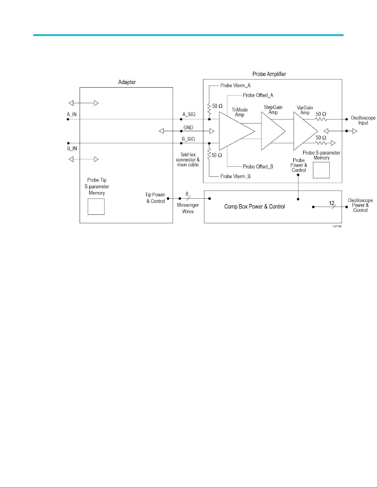
The following figure shows a simplified diagram of the TekFlex active probe tip architecture.
Figure 4: TDP7700 Series TriMode probe input architecture
The TekFlex active probe tip has two inputs, A_IN and B_IN, which can, depending on the tip design, support TriMode
measurements. With a TriMode tip, such as a TekFlex solder-in tip, it is possible to make differential, single-ended A, singleended B, and common-mode measurements, all from a single soldered differential signal connection to a DUT. The
soldered wire connections between the two probe tip input signal vias and DUT differential signal nodes should be kept as
short as possible (as should the ground via connections if single-ended measurements will be made). The A and B input
signals on the probe tip pass to a matched pair of damping resistors, Rd, that isolate the probe connection to the DUT. The
TDP7700 Series TriMode™ Probes Technical Reference 4
Page 13

Theory of operation
damping resistor value of approximately 100 Ω also serves to tune the probe tip high frequency response. Following each
input damping resistor is a pair of attenuation resistors, Rs and Rp. The attenuation resistor values depend on the specific
probe tip attenuation factor design. There are currently two attenuation factors available as shown in the following table with
approximate attenuation resistor values. The probe tip attenuation factor in the table includes an additional 2X factor due to
attenuation from the 50 Ω tip buffer output impedance and the 50 Ω probe amplifier termination impedance.
Table 1: Probe tip attenuation factors
Attenuation factor Rs Rp Dynamic range Offset voltage range
4x 25 kΩ 25 kΩ 2.5 V
10x 60 kΩ 15 kΩ 6.0 V
pp
pp
±4.0 V
±10.0 V
The input attenuation resistors serve three major functions for the dual input tip buffer:
• The high resistance of the attenuation resistors provides very light loading on the probe input signals.
• The probe tip attenuation factor expands the linear dynamic range of the probe tip inputs.
• The probe tip attenuation network provides a resistive summing junction for injecting an offset voltage signal to extend
the probe tip operating voltage window.
TekFlex active tips contain a pair of unity gain amplifiers that buffer the DUT differential input signal. These buffer amplifiers
provide an impedance conversion for the input signals from the high impedance input attenuator at the tip input to the 50 Ω
output drive at the tip output. The buffer amplifier 50 Ω output impedance is needed to drive the probe TekFlex connector
and meter-long main cable transmission lines with good high frequency fidelity. The new TekFlex interface to which TekFlex
probe tips are attached includes both a dual high frequency connection for the probe tip signals as well as a low frequency
connection for eight messenger wires that provide power and control for the active probe tips.
The control features of the new TekFlex interface include two analog tip offset voltage signals and a pair of digital
communication signals for accessing the probe tip S-parameter memory.
The probe tip S-parameter memory contains characterization data for use with DSP correction filters that are unique to the
probe tip. The S-parameter memory includes a unique data header used in automatically identifying the probe tip type and
serial number. The A and B signal outputs from the probe tip are connected by high frequency spring contacts in the
TekFlex connector to a pair of delay-matched coaxial cables that carry the input signals through the main cable and into the
comp box. These signals terminate to a pair of 50 Ω termination resistors at the probe amplifier in the comp box. The
termination resistors have an adjustable termination voltage connection for optimal loading of the probe tip output signals.
The TekFlex interface messenger wires are routed as a small gauge ribbon cable, along with the delay-matched coaxial
cables, inside a shielded main cable assembly.
The TDP7700 Series probe amplifier has several cascaded amplifier stages that condition the probe tip differential signal for
precision measurement fidelity. The complex input stage of the probe amplifier selects the desired TriMode input mode.
This input stage of the probe amplifier includes connections for injecting a pair of adjustable probe offset voltages for
precision control of the probe output zero voltage, which is a measure of the output signal with volts at both probe tip inputs.
The next stage in the probe amplifier is the step gain stage. The step gain stage provides several switchable, coarse gain
steps, that extend the sensitivity range of the probe measurement down to the millivolt level with good noise performance.
The step gain stage is automatically switched to its optimum setting by the oscilloscope as the oscilloscope vertical channel
sensitivity is adjusted by the user.
The final stage of the probe amplifier is the variable gain stage. The variable gain stage is used for fine tune adjustment of
the gain of the probe and probe tip to its calibrated value. The calibrated gain setting is determined from calibration
constants characterized during manufacturing testing of the probe and probe tip and includes compensation for probe
temperature variation. Although the signal that passes through the probe amplifier is processed as a differential signal
through the internal amplifier stages, it is routed to the oscilloscope’s TekVPI interface as a single-ended output.
TDP7700 Series TriMode™ Probes Technical Reference 5
Page 14

Theory of operation
The ground path for high frequency signal return currents is shown in the probe architecture figure. (See Figure 4: TDP7700
Series TriMode probe input architecture on page 4.) The probe ground path is continuous and along the following path:
• Extends from the DUT ground vias connections at the probe tip input
• Through the probe tip ground path
• Through the TekFlex connector ground spring contacts
• Along the main cable coaxial shields into the probe comp box
• Through the probe amplifier circuit board ground plane inside the probe comp box, and
• Through the TekVPI interface to the host oscilloscope ground
A TriMode tip requires a short DUT ground reference for making low noise single-ended probe measurements.
Although two ground via connections are available on the probe tip input, a single ground via wire connection is usually
adequate for making single-ended measurements of both the A and B input signals or a common-mode measurement, all of
which are ground referenced.
If only one single ended signal will be connected to the probe, the user has the choice of connecting the A input to the
signal and the B input to ground, or connecting the A input to the signal and the ground input of the probe to the ground
input of the DUT. In this situation, Tektronix recommends using A-B mode with the B input connected to ground. Reasons for
this recommendation include that with the B input left disconnected, there is a possibility of an interfering signal coupling into
the input of the probe and distorting the measured signal acquired on the A side.
A second reason for using A-B vs. A-ground is that it is often more convenient to connect the differential inputs of the probe
to a device and keep the wire lengths short. The ground connections of the probe are set back from the tip and may not be
as convenient to connect to a DUT with tightly spaced test points.
The optional accessory P77BRWSR is a variable-spacing probe tip which operates in Differential Input mode only. The
P77BRWSR Browser probe tip does not have a physical ground connection at the probe tip; but the differential
measurement process itself provides a high frequency virtual ground connection between the A and B signal input pins. A
low frequency ground connection is optionally available at a square-pin socket on the browser probe tip housing.
The comp box receives power and control signals from the oscilloscope through the TekVPI interface. The TekVPI interface
is an intelligent probe connection that includes many automated and manual control features. For example, there is a probe
S-parameter memory in the comp box that stores high frequency characterization data for the probe signal path.
The downloaded S-parameter data for a probe and attached probe tip is used by the oscilloscope to generate a DSP
correction filter for optimum measurement fidelity. Because this S-parameter data is unique and serialized for each probe
and probe tip, it only needs to be downloaded once to an oscilloscope.
Automatic probe tip type identification is another example of the intelligent operation of the TDP7700 Series probes. When
no probe tip is attached to the TekFlex connector of a TDP7700 Series probe, the TekFlex probe tip interface power is
disabled. When a probe tip is attached to the TekFlex connector, the attachment is detected by the probe and the probe
queries the probe tip memory to check for a valid identification header. If a valid probe tip type is verified by this TekFlex
data interface query, the probe tip power is enabled until the probe tip detachment is detected.
When probe tip power is enabled, an LED is activated on the probe tip, indicating that the TekFlex interface and attached
probe tip appear to be operating properly. If the probe tip type attached to the TekFlex connector is a browser probe tip, the
probe tip automatically detects the current tip spacing and communicates that information to the oscilloscope.
There are several calibrated tip spacing regions defined for the browser tip, which affect the frequency response of the
browser tip signal. Wider tip spacing tends to degrade the browser tip frequency response. The oscilloscope uses the
current tip spacing region information to select the optimum DSP correction filter for use with the browser tip measurements.
Input architecture with the P77C292MM SMA adapter
The P77C292MM adapter is a passive probe adapter; there are no active components within the adapter. It is intended to
connect the TDP7700 series probes to 50 Ω RF test points.
TDP7700 Series TriMode™ Probes Technical Reference 6
Page 15
Theory of operation
The following figure shows the simplified diagram of the TDP7700 Series TriMode probe input architecture with the
P77C292MM SMA adapter. Because there are no active components within the adapter the A and B inputs are passed
through directly to the probe amplifier.
Figure 5: TDP7700 Series TriMode probe input architecture with the P77C292MM SMA adapter
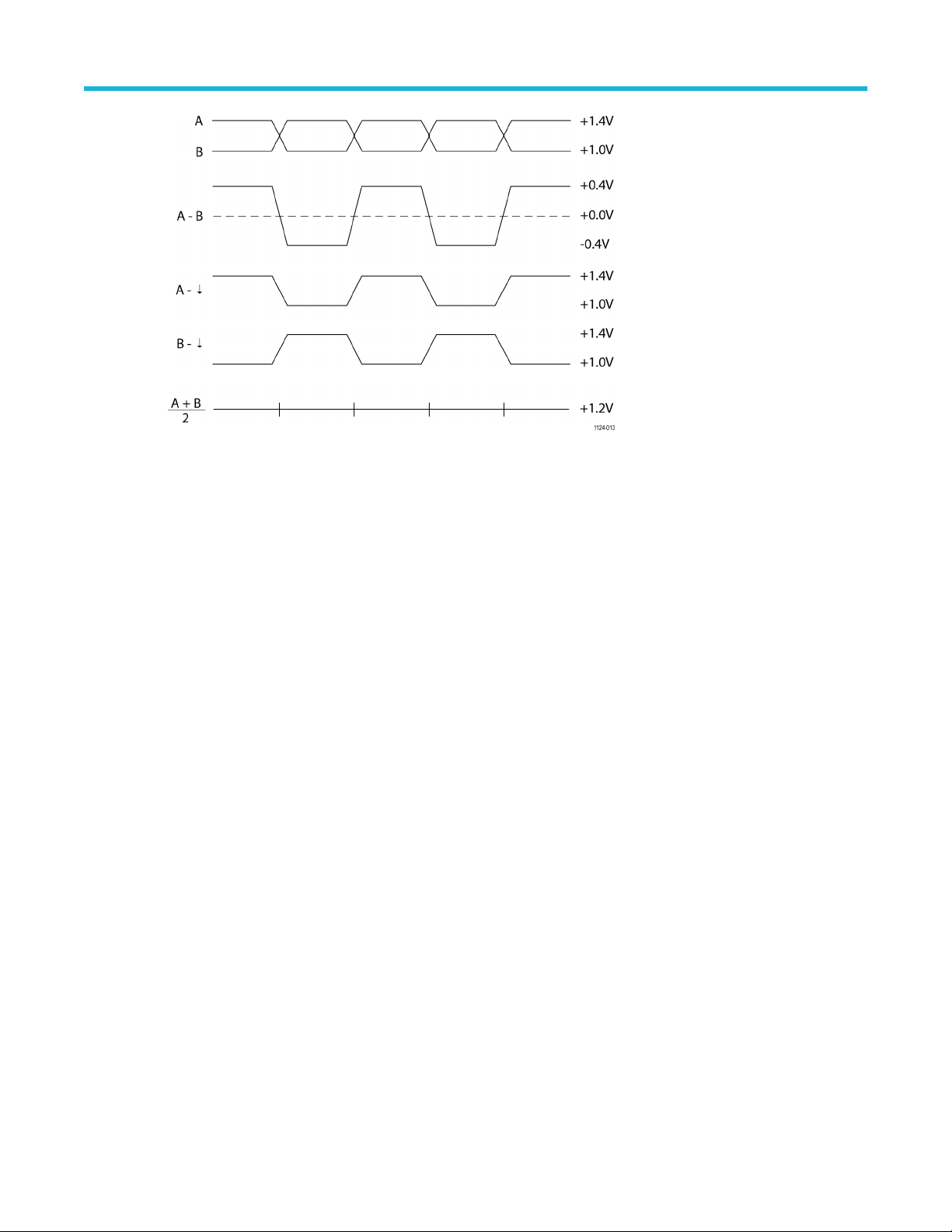
TriMode operation
The TriMode feature of the TDP7700 Series probes is designed for improved convenience and enhanced capability in
measuring differential signal quality. Because a differential signal is composed of two complementary single-ended signals,
full characterization of a differential signal requires more than a simple differential measurement.
A TriMode probe features four input modes that allow a differential signal to be fully characterized with four measurements:
• Differential
• Positive polarity, single-ended
• Negative polarity, single-ended
• Common mode
A TriMode probe provides improved efficiency and convenience by enabling full differential signal characterization from a
single soldered connection.
TekFlex active probe solder tips support the TriMode functionality of a TDP7700 Series probe by buffering a matched pair of
input signals from a DUT differential signal connection. These active solder tips support the transmission of high-frequency
return currents through a probe tip ground path referenced to the DUT ground connection.
Using any of the TekFlex solder-in tips, probe connections are made to the two complementary signals (the A signal and the
B signal) and a ground reference. From this single DUT connection, the internal electronic switching control of the TriMode
probe allows any one of the four probe input modes to be selected at a time. The TriMode probe inputs are routed to an
ASIC (application-specific integrated circuit) inside the probe to a set of four independent input amplifiers that perform the
following signal calculations:
• A – B (for differential signal measurement)
• A – GND (for A input single-ended measurement)
• B – GND (for B input single-ended measurement)
TDP7700 Series TriMode™ Probes Technical Reference 7
Page 16

Theory of operation
• [A+B]/2 - GND (for common mode measurement)
Note: In the B – GND Mode, the negative polarity B input is not inverted.
The four input amplifiers are multiplexed together and only the selected input mode function is sent to the connected
oscilloscope. The following figure shows a conceptual view of the TriMode probe input structure, where the C input provides
the probe ground reference and is connected to the probe tip ground interconnect using the probe’s cable coaxial shields.
Figure 6: TriMode input structure
Operating voltages
The TDP7700 Series probes are designed to probe high-frequency, low-voltage circuits. Before probing a circuit, take into
account the limits for the operating voltages discussed in this section.
• Max non-destruct input voltage
• Input signal dynamic range
• Offset voltage
• Operating voltage window
TDP7700 Series TriMode™ Probes Technical Reference 8
Page 17

Figure 7: TekFlex probe tip inputs
Theory of operation
Max non-desctruct input voltage
The maximum input voltage is the maximum voltage to ground that the inputs can withstand without damaging the probe
input circuitry. The TekFlex active probe tips include some over-voltage protection circuitry at the probe tip signal inputs.
(See Figure 7: TekFlex probe tip inputs on page 9.) Transient voltage suppression diodes, Da and Db, provide bidirectional
voltage clamping of signals applied to the probe tip inputs. These TVS diodes limit potential ESD damage as well as signal
over-voltage damage to the active tip buffer amplifier device.
CAUTION: To avoid damaging the inputs of the probe, do not apply more than ±15 V (DC + peak AC) between
either probe input and ground.
CAUTION: To avoid ESD damage to the probe, always use an antistatic wrist strap (provided with your probe), and
work at a static-approved workstation when handling the probe.
Input signal dynamic range
The input signal dynamic range is bound by the maximum voltage difference between either the A and B input of the probe
tip and the probe tip ground reference that the probe can accept without distorting the signal. Outside of the input signal
dynamic range, gain compression will result in increased linearity error and clipping. The DC specifications of the probe are
valid only over the input signal dynamic range. The dynamic range is not a hard limit for signal distortion; probe tip input
voltages can slightly exceed the dynamic range limit if a slightly higher linearity error is determined to be acceptable.
The differential and common-mode dynamic ranges for TekFlex probe tips are derived from the single-ended dynamic
range. The maximum differential signal can be twice the single ended range since the A side can be at the positive dynamic
range limit and the B side can be at the negative dynamic range limit (or vice versa). The maximum common-mode signal is
the same as the single-ended dynamic range limits. With the probe tip A and B offset voltages both set to 0 V, the dynamic
range will be symmetrical around that 0 V level. In this case, the dynamic range can be considered to equal ±(dynamic
range ÷ 2). If the oscilloscope vertical scale factor is set high enough to display the full dynamic range, the oscilloscope will
momentarily add dynamic range limit annunciation lines. These dynamic range annunciation lines can be refreshed by
adjusting one of the vertical channel knobs, such as position or scale factor.
TDP7700 Series TriMode™ Probes Technical Reference 9
Page 18
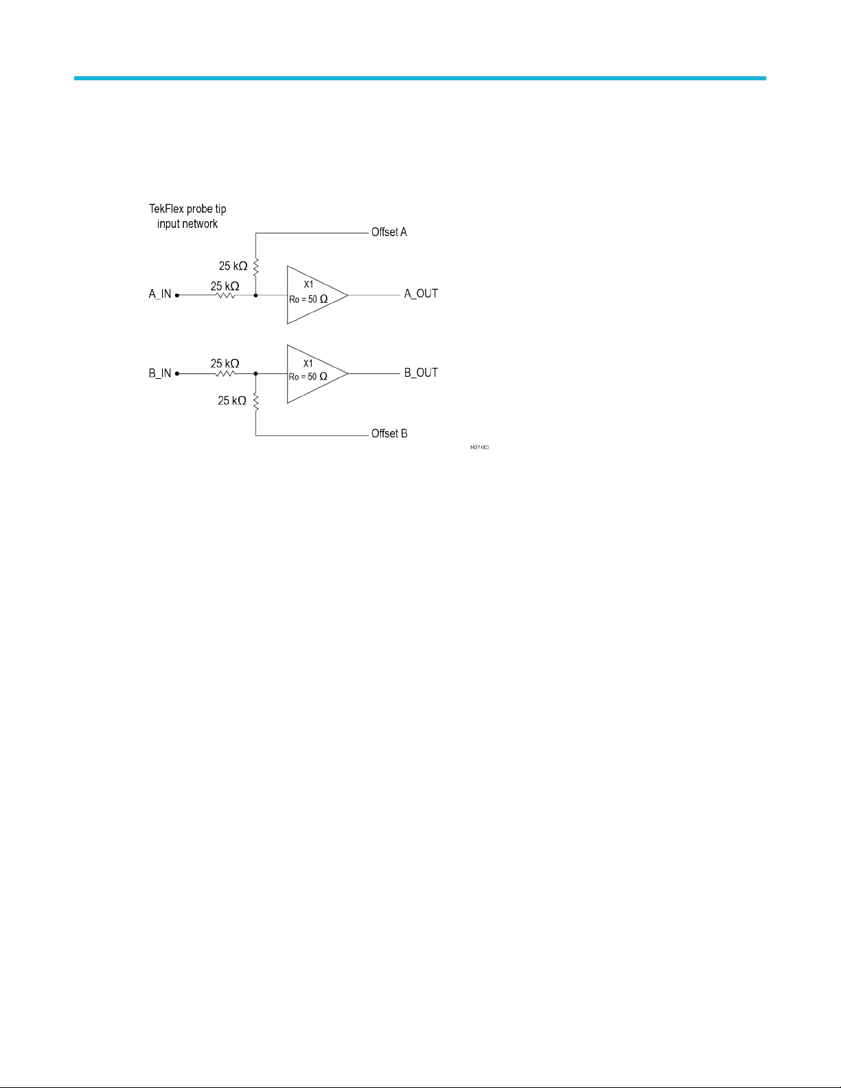
Offset voltage
The offset voltage control sums an adjustable DC voltage with the probe signal input. It is commonly used to nullify an input
DC bias voltage to center the input signal swing within the linear dynamic range of the probe input. The A and B probe
inputs both have an independent offset voltage control when used in A mode or B mode respectively. The following figure
shows a simplified diagram of a TekFlex probe tip input network.
Theory of operation
Figure 8: Simplified diagram of the TekFlex probe tip input network
The offset voltage affects the probe tip buffer’s measured signal through a resistive summer configuration that forms the
buffer’s input attenuator network. The high value resistors used in the input attenuator result in an interaction between the
input signal and the offset voltage DC level.
Calibrated offset voltage performance requires both the input signal and the offset voltage generator in the probe have a
source resistance that is very small compared to the 25 kΩ attenuator resistors. The source resistance (Rs)of the offset
voltage generator in the probe is less than 1 Ω and measured DUT signals typically have Rs << 25 kΩ. If a probe tip is
attached to a probe TekFlex connector with its probe tip inputs open, the input signal source resistance is much larger than
the 25 kΩ attenuator resistors. As a result, the offset voltage control is no longer calibrated and will have twice the calibrated
effect on the measured probe output.
The offset voltage control, accessible from the attached oscilloscope front-panel control and the on-screen user interface,
allows the probe dynamic range to be effectively moved up and down within the limits of the offset voltage range and the
operating voltage window. When the offset voltage is set to zero volts and the input signal is zero volts (inputs shorted to
ground, not open), the displayed signal should be zero volts. If a noticeable zero volt offset is present under the above
conditions, an oscilloscope SPC and an autozero operation should be performed.
In A or B mode, the single-ended offset can be controlled through the probe menu. In C or D mode, both the differential or
common-mode offsets can be controlled through the probe menu. The single-ended offsets are related to the differential/
common-mode offsets by the following relationships:
• Differential = (A - B)
• Common = (A + B)/2
• A = Common + (Differential/2)
• B = Common - (Differential/2)
The offset range limits apply to each side of the single-ended inputs. Due to this, the common-mode and differential offset
ranges are limited to the area shown in the diamond-shaped graph below. When the maximum differential offset is applied,
the common-mode offset is restricted to 0V. Similarly, with the maximum common-mode offset applied, the differential offset
is constrained to 0V.
TDP7700 Series TriMode™ Probes Technical Reference 10
Page 19

Theory of operation
It is additionally possible to turn on an Autotracking function. In C-mode, the autotracking function adjusts the offsets to null
out the low-frequency differential input seen by the probe amplifier, maximizing the common-mode dynamic range. In D
mode, the autotracking function adjusts the offsets to null out the low-frequency common-mode input seen by the probe
amplifier, maximizing the differential dynamic range.
Figure 9: Simplified Auto Tracking circuitry
The A and B input signals are buffered by the active probe tip buffer amplifier and passed down the probe main cable
assembly into the comp box probe amplifier input pins. The A and B input signals are picked off inside the probe amplifier
with large value resistors and output to an averaging filter capacitor as Sense_A and Sense_B signals. These sense signals
TDP7700 Series TriMode™ Probes Technical Reference 11
Page 20

are buffered by a pair of unity gain amplifiers and passed to the comp box microcontroller ADC conversion inputs. The
converted sense signals are transmitted to the oscilloscope when requested by an Auto Offset cycle, where they are
processed by the oscilloscope according to the selected Auto Offset mode. The processed mean value or individual A and B
offset values are sent back to the probe microcontroller, which drives the tip offset DAC signals accordingly.
Operating voltage window
Voltage window
The operating voltage window defines the input signal voltage range within which probe measurements can be made with
good fidelity. The operating voltage window limits is a function of input dynamic range, offset and, in the case of the
P77C292MM adapter, V
a tip. The smaller green box illustrates the dynamic range considering specific offset levels. The dynamic range square can
be moved around within the operating window by adjusting the A and B offset settings.
Theory of operation
. In the figures below, the grey area demonstrates the range of signals that can be measured by
term
Figure 10: Operating voltage window (TekFlex solder-in tips)
The A operating voltage window range of ±5.25 V is shown on the vertical axis and the B operating voltage window range of
±5.25 V is shown on the horizontal axis. The dynamic range is also shown on the figure as the smaller green square. The
TekFlex solder tip single-ended dynamic range for both the A and B inputs is 2.5 V
range is 5 V
p-p
.
. Differentially, the solder tip dynamic
p-p
Because there are several step gain values available within the TDP7700 Series Probe Amplifier, the actual size of the
dynamic range square depends upon the oscilloscope vertical scale factor setting. The vertical scale factor determines the
required probe amplifier step gain setting, which is automatically set to the proper value under the oscilloscope control.
The dynamic range square is set to its full-size 2.5 V
settings that a 2.5 V
signal can be fully displayed on the oscilloscope. As the vertical scale factor is set to lower V/div
p-p
setting when the vertical scale factor is set to large enough V/div
p-p
settings, the probe amplifier step gain threshold will eventually be reached and the step gain value will be increased by one
step. In C and D mode, only common-mode and differential offset adjustments are possible. For active tips, this is
represented by the one-dimensional figures below.
Figure 11: Operating voltage window (diferential mode, flex tip)
TDP7700 Series TriMode™ Probes Technical Reference 12
Page 21

Figure 12: Operating voltage window (common mode, flex tip)
Voltage window with P77C292MM SMA adapter
The P77C292MM adapter operating voltage window is shown in the following figure.
Theory of operation
Figure 13: Operating voltage window (P77C292MM SMA adapter)
The A operating voltage window range for the adapter of ±4.0 V is shown on the vertical axis and the B operating voltage
window range of ±4.0 V is shown on the horizontal axis. The dynamic range is also shown on the figure as the smaller
green square.
Similar to the operating voltage for the TekFlex solder-in tips, the dynamic range square labeled Small Signal AC can be
moved around within the limits of the operating voltage window by adjusting the A and B offset voltage settings. The A and
B offset voltage values determine the location of the center of the dynamic range square in the operating voltage window
plot. In C and D mode, only the common-mode and differential offsets are available. These operating windows are
illustrated by the figures below.
Figure 14: Operating voltage window (differential mode, P77C292MM adapter)
Figure 15: Operating voltage window (common mode, P77C292MM adapter)
TDP7700 Series TriMode™ Probes Technical Reference 13
Page 22

Theory of operation
The P77C292MM adapter has a further dimension that effects the operating window. The V
dynamic range. A plot of V
and valid input voltages is shown in the Overload Specification section.
term
Improving measurement accuracy
DSP correction filtering
TDP7700 Series probes and probe tips use DSP correction filtering to optimize probe measurement fidelity. High frequency
time domain measurement performance characteristics such as rise time, aberrations, and pulse flatness are improved by
DSP correction filtering. Similarly, frequency domain performance characteristics such as bandwidth, frequency response
flatness, and differential signal coupling are improved by DSP correction filtering. DSP correction filtering is performed
automatically by the oscilloscope using S-parameter characterization data downloaded from probe and probe tip storage
memories. This S-parameter data is unique for each probe and probe tip, rather than the nominal response data that was
used in some previous generation probe families.
Distinct S-parameter data sets are stored in probe memory for each probe input mode and step gain setting combination.
Every different input mode and step gain combination has a slightly different amplifier signal path, which requires different
signal response correction. Since the solder tip buffers do not have complex mode switching, only one S-parameter data set
is stored in the probe tip storage memory. The high frequency signal performance of the P77BRWSR browser tip changes
slightly as the tip spacing is adjusted. Several S-parameter data sets are stored in the browser tip memory and
automatically switched to the optimum data set, under control of the browser tip spacing position detection circuitry.
S-parameter characterization data are measured for each probe and probe tip as part of the manufacturing test process.
TDP7700 Series probe signal performance is measured using a 3-port VNA measurement configuration with a 2-port
TekFlex connector input and a 1-port TekVPI interface output. Custom test fixtures have been developed for making VNA
port connections to the probe TekFlex connector input and TekVPI interface output. Test fixtures designed for connecting to
the probe input and output signal ports are de-embedded to remove interconnect losses and signal path imperfections.
setting influences the
term
TekFlex probe tip signal performance is measured using a 4-port VNA measurement configuration with 2-port input and
output connections. Because the TekFlex probe tips do not have standard RF connectors at their inputs or outputs, the
custom test fixtures inject and receive VNA port signals. Custom calibration standards were developed to support deembedding these probe tip manufacturing test fixtures.
Solder-in tip connection wire length
There are four via locations for soldering wire connections between the probe tip and the measurement DUT.
The via connections include the probe tip A and B inputs for a differential signal and two ground connections for best
performance and flexibility in connecting to a close DUT ground. In general, the probe tip soldered wire connection length
should be kept as short as possible. In addition, the probe tip A and B input wires should be matched in length for best
differential mode measurement performance.
The differential input mode does not require a ground reference wire connection, since the differential measurement
process provides its own virtual ground. The single-ended input modes, which include A-GND mode, B-GND mode, and
common mode, all require at least one ground wire connection.
While only connecting the differential inputs of the probe is required and is most convenient, if there is room for another
connection and a circuit ground near the probe tip, connecting to a ground connection is recommended. Connecting the
ground can help avoid a situation where a large potential on the ground of the DUT causes the test signal to drift outside of
the linear range of the input amplifier of the probe. Ideally, it is a good idea to connect the differential inputs and the ground
to avoid clipping of the signal in the probe amplifier.
The measurement performance of all input modes is affected by the length of the input wire connection, with high frequency
performance degradation increasing with increased wire length.
The measurement performance of the single-ended input modes is affected by the length of the ground wire connection,
with high frequency performance degradation also increasing with increased ground wire length. The TekFlex solder-in
TDP7700 Series TriMode™ Probes Technical Reference 14
Page 23

Theory of operation
probe tip performance is specified using a test fixture built with a probe tip having a signal wire length of 10 mils (.25 mm)
and a ground wire length of 66 mils (1.7 mm).
The typical pulse waveforms in the following figures show the effect of input wire length variation on measured responses.
Note that these measurements, in these images, were made using a 20 Ghz P7720 probe.
Figure 16: P77STFLXA solder tip attached with 10 mils (0.250 mm) wires (rise time = 30.5 ps)
Figure 17: P77STFLXA solder tip attached with 75 mils (1.90 mm) wires (rise time = 27.9 ps)
TDP7700 Series TriMode™ Probes Technical Reference 15
Page 24
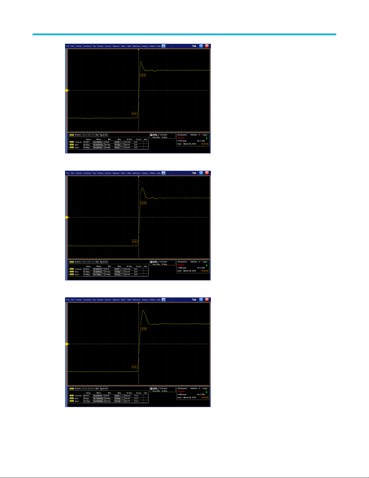
Figure 18: P77STFLXA solder tip attached with 120 mils (3.05 mm) wires (rise time = 30.1 ps)
Theory of operation
Figure 19: P77STFLXA solder tip attached with 200 mils (5.08 mm) wires (rise time = 34 ps)
Figure 20: P77STFLXA solder tip attached with 300 mils (7.62 mm) wires (rise time = 42.8 ps)
The following table shows the rise time and overshoot degradation versus lead length.
TDP7700 Series TriMode™ Probes Technical Reference 16
Page 25

Table 2: Rise time and overshoot degradation versus lead length
Signal wire lead length 10 - 90 Rise time 20 - 80 Rise time Effective bandwidth
0.25 mm 30.5 ps 21 ps 20 GHz
1.90 mm 27.9 ps 19.3 ps 20 GHz
3.05 mm 30.1 ps 20.9 ps 20 GHz
5.08 mm 34 ps 23.6 17 GHz
7.62 mm 42.8 ps 29.2 14 GHz
Using offset voltage to extend TekFlex® solder-in tip input voltage range
Theory of operation
The single-ended linear dynamic range of the TekFlex solder-in tip inputs is specified to be 2.5 V
, which is a range from
p-p
-1.25 V to +1.25 V with zero volt offset. The dynamic range of buffers is limited by the input attenuation factor, which is 2X
for the solder-in probe tips as shown in the following simplified figure. A 2X attenuation factor was selected for the probe tips
to optimize dynamic range and noise, since a higher attenuation factor would have increased probe noise. Although the
dynamic range of the probe tip buffer cannot be extended, it is possible to extend the range over which the tip dynamic
range window can be moved by adjusting the probe offset voltage. The offset voltage range of the TekFlex solder-in tips is
-4 V to +4 V, which is adjusted using the Probe Setup screen of the oscilloscope or the offset knobs on the oscilloscope
front panel. Using the offset voltage controls, it is possible to make measurements within any 2.5 V
window between
p-p
-5.25 V and +5.25 V. As an example, by setting the offset voltage to +3.0 V, it is possible to measure an HDMI signal, which
has a signal swing between about +2.8 V and +3.3 V.
Figure 21: Simplified diagram of the TekFlex probe tip input network
The offset voltage affects the probe tip buffer’s measured signal through a resistive summer configuration that forms the
buffer’s input attenuator network. The high value resistors used in the buffer’s input attenuator result in an interaction
between the input signal and the offset voltage DC level.
Calibrated offset voltage performance requires that both the input signal and the offset voltage generator in the probe have
a source resistance that is very small compared to the 25 kΩ attenuator resistors. The source resistance of the offset
voltage generator in the probe is less than 1 Ω. Typically, when the probe and tip are connected to a DUT, the DUT signals
have a source resistance Rs much less than 25 kΩ.
TDP7700 Series TriMode™ Probes Technical Reference 17
Page 26
If a probe tip is attached to a probe but not soldered to anything, the inputs will be open which effectively makes the source
resistance look much larger than the 25 kΩ attenuator resistors. As a result, the offset voltage control is no longer calibrated
and will have 2X the calibrated effect on the measured probe output. This effect can be helpful in troubleshooting
connection issues with the tips. If a probe tip has been soldered to a DUT and adjusting the offset voltage causes the offset
to move 2X the adjustment, it could indicate a broken solder joint that has left the probe tip input open.
Making single ended measurements using the P77BRWSR differential probe tip
A TriMode tip provides solder connections for a DUT ground reference for both the A and B probe inputs making singleended measurements with a TriMode probe tip straightforward. Although the differential input mode of the probe is normally
used to make a differential signal measurement, single-ended measurements can be made using Differential Input mode
when the probe input connections and offset voltage controls are configured properly, This single-ended configuration
process is particularly important to understand when using the tip, since this variable-spacing Browser tip operates only in
Differential Input mode. Differential Input mode provides a measurement of the difference (A – B) between the A and B input
signals. If the probe tip B input is connected to a DUT ground, the resulting Differential Input mode measurement (A – 0 V)
results in a display of the single-ended A input signal response.
When making differential signal measurements, the P77BRWSR Offset Voltage control is normally set to the Commonmode (CM) Tracking mode. With CM tracking mode active, the A and B input signals are monitored and the Offset A and
Offset B settings are both adjusted to match the DC common-mode voltage of the A and B input signals [(A + B)/2]. The
differential Offset voltage should be set manually to the center of the signal voltage swing. The common mode offset should
be set to 1/4 of the signal swing. For a +5 V CMOS logic signal; for example, the differential offset voltage should be set to
+2.5 V and the common mode offset should be set +1.25V. The A signal input voltage should then range from +5 V to 0 V,
which is within the 6 Vp-p dynamic range of the Browser tip as long as the offset voltage is set near the center of its
expected voltage swing. These offset settings maximize the dynamic range of single ended measurements for the
differential browser.
Theory of operation
Temperature compensation
The TDP7700 Series probes employ temperature compensation to optimize measurement accuracy.
Active tip measurement configuration
In many of the high-frequency signaling standards that the TDP7700 Series probes are designed for, a 50 Ω termination at
the transmitter is in parallel with another 50 Ω termination at the end of the transmission line path, effectively making a 25 Ω
signal source impedance. In this application, the solder tip or browser tip measurement configuration is designed to pick off
the transmitted signal at a location in the signal transmission path.
The input impedance for a solder tip, Z probe, varies with frequency. For a TekFlex solder tip the DC input resistance is
about 50 kΩ and decreases with frequency above about 10 MHz to about 100 Ω above 10 GHz. Refer to the graphs later in
this document for input impedance information. See page Impedance graphs on page 25.
Figure 22: Active tip measurement configuration
Skew measurements of differential signals
Differential signals are composed of two complementary single-ended signals that generally swing around a common bias
voltage. An example of an LVDS differential signal is shown in the following figure.
TDP7700 Series TriMode™ Probes Technical Reference 18
Page 27
Theory of operation
Figure 23: Example of LVDS differential signal
The complementary single-ended signals labeled A and B in the previous figure must have well matched signal timing (for
example, low skew) to function as a useful differential signal. If the signal skew becomes comparable in size to the rise time
of the complementary signals, then the rise time of the resulting differential signal will be slower than expected. Skew is a
measure of the time delay mismatch between two supposedly matched signals.
Although very accurate low skew measurements usually require TDR or VNA measurement equipment, it is possible to
make relatively accurate skew measurements of a differential signal pair using a TDP7700 Series probe and a TekFlex
probe tip. A flex circuit based solder tip should first be soldered to the DUT differential signal, taking care to match the A and
B input wire lengths, because the wiring length mismatch will contribute to the skew measurement error. A DUT ground
reference connection should also be made to one of the TekFlex tip ground vias using a wire length as short as possible.
At first it might seem reasonable to try to make a skew measurement by directly comparing the A and B signal timing.
Although it is possible to display both the single-ended A and B signals that make up the differential signal using the
TriMode measurement selection function, both signals cannot be displayed with a single signal acquisition of the
oscilloscope. Even though it is possible to capture the A signal and store it as a reference waveform for comparison with a
follow-on B signal acquisition, the trigger timing uncertainty between acquisitions might make this a less than accurate, if not
impossible approach.
A more indirect, but more accurate, skew measurement is possible by switching the probe input mode to the common mode
setting. Because the common mode setting for a TekFlex probe tip features full probe bandwidth, the response should be
fast enough to display the relative skew performance. The common mode response for a perfectly matched, zero skew,
complementary signal pair should be a flat trace at the common DC bias voltage level. As the skew of the signal pair
increases, the common mode waveform begins to show narrow pulses at the signal logic transitions. The pulse width of
these narrow transition pulses is a relative measure of the skew.
TDP7700 Series TriMode™ Probes Technical Reference 19
Page 28

Reference
This section defines common terms used to specify the instrument.
Differential measurements
A differential probe is optimized to measure high speed differential signals. Differential signals are formed from two
complementary signals with a common reference voltage. (See Figure 24: Simplified model of a differential amplifier
on page 20.)
Devices designed for differential measurements avoid problems presented by single-ended systems. Differential signal
transmission improves signal fidelity by doubling the effective signal amplitude compared to single-ended signal
transmission. Differential signaling also improves signal fidelity by removing common mode noise due to the CMRR of the
receiver or measurement device.
A differential probe is basically a differential amplifier used to make differential measurements that reject any voltage
common to the inputs and amplifies any difference between the inputs. Voltage that is common to both inputs is often
referred to as the common-mode voltage (VCM) and voltage that is different as the differential mode voltage (VDM).
Reference
Figure 24: Simplified model of a differential amplifier
Common-mode rejection ratio
Differential amplifiers cannot reject all of the common-mode signal. The ability of a differential amplifier to reject the
common-mode signal is expressed as the common-mode rejection ratio (CMRR).
The DC CMRR is the differential-mode gain (ADM) divided by the common-mode gain (ACM). It is expressed either as a ratio
or in dB:
AC CMRR for the probe is determined using 3-port, mixed-mode S-parameters for the measured differential mode
response, where A input = Port 1, B input = Port 2 and Output = Port 3 is defined as:
TDP7700 Series TriMode™ Probes Technical Reference 20
Page 29

Reference
The 6 dB term in the AC CMRR equation gives the voltage-referenced response. CMRR generally is highest (best) at DC
and degrades with increasing frequency. A typical CMRR plot for a TDP7700 Series probe and a flex circuit-based solder tip
is shown.
Figure 25: Typical CMRR
Assessing CMRR error
The CMRR of the TDP7700 Series probes is shown in graphs assuming a sinusoidal common-mode signal. A quick way to
assess the magnitude of CMRR error when the common-mode signal is not sinusoidal is to connect both leads to the same
point in the circuit. The oscilloscope displays only the common-mode component that is not fully rejected by the probe.
While this technique might not yield accurate measurements, it allows you to determine if the magnitude of the commonmode error signal is significant. When using the solder-in tips, keep the tip leads the same length to maximize the probe
CMRR.
Input impedance effects on CMRR
The lower the input impedance of the probe relative to the source impedance, the lower the CMRR for a given source
impedance imbalance. Differences in the source impedance driving the two inputs lowers the CMRR. Note that singleended measurements generally result in asymmetric source impedances which tend to reduce the differential mode CMRR.
Differential-mode rejection
When making common-mode signal measurements ((A+B)/2 – GND) with the TriMode probe, it is desirable to reject the
differential-mode signal present between the two inputs. This rejection is expressed as the Differential-Mode Rejection Ratio
(DMRR).
AC DMRR for the probe is defined using 3-port, mixed-mode S-parameters as:
for the measured common mode response. The 6 dB term in the AC DMRR equation gives the voltage-referenced
response.
Channel isolation
Under ideal conditions when taking single-ended measurements with a differential probe, no part of a signal applied to one
input of the probe would appear on the other input. In reality some portion of the signal on one input does “bleed” over to the
TDP7700 Series TriMode™ Probes Technical Reference 21
Page 30
Reference
other input, and this effect increases with frequency. Channel isolation is a measure of how much crosstalk occurs between
the two probe inputs. The channel isolation is defined with S-parameter measurements below, where:
A input = S1, B input = S2, Output = S3
A ISOLATION = 20 log (S31/S32) | A Mode
B ISOLATION = 20 log (S32/S31) | B Mode
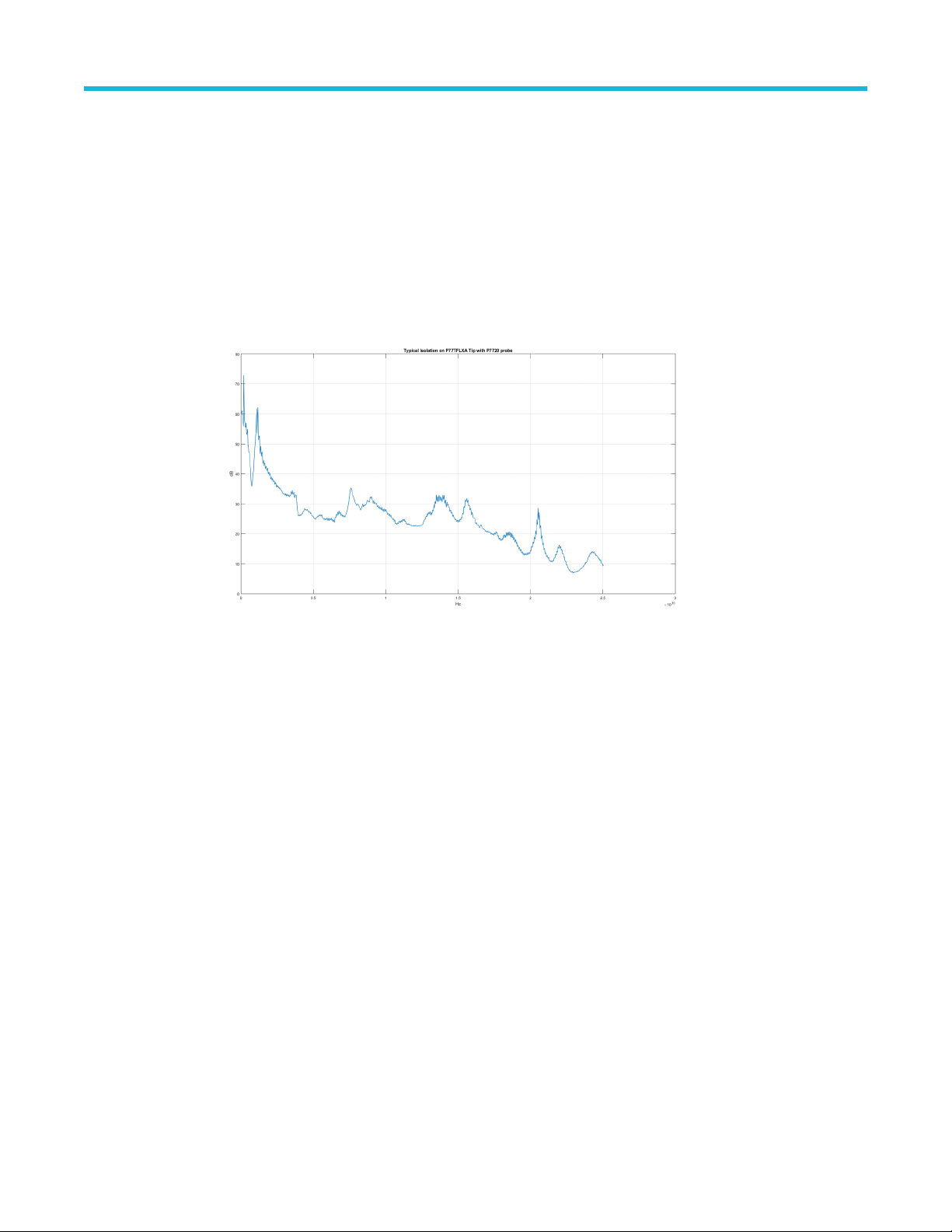
A typical isolation plot for the TDP7700 Series probes using a TekFlex solder tip is shown in the following figure. When the
probe is used with TekFlex solder tips, note that channel isolation performance is highly dependent on probe tip attachment
lead length. Good channel isolation requires keeping the interconnect lead length for both signal and ground connections
very short.
Figure 26: Typical channel isolation
TDP7700 Series TriMode™ Probes Technical Reference 22
Page 31
Specifications
These specifications apply to the TDP7700 Series probes when installed on an 6 Series MSO oscilloscope with a bandwidth
greater than or equal to 10 GHz. The probe performance may be degraded if a probe is operated using an oscilloscope with
bandwidth less than the probe bandwidth. The probe and oscilloscope must have a warm-up period of at least 20 minutes
and be in an environment that does not exceed the allowed environmental limits. (See Environmental on page 27.)
Output zero, typical ±4 mV
Linearity, typical ±1%
Termination voltage range, typical ± 2.5 mV.
Specifications
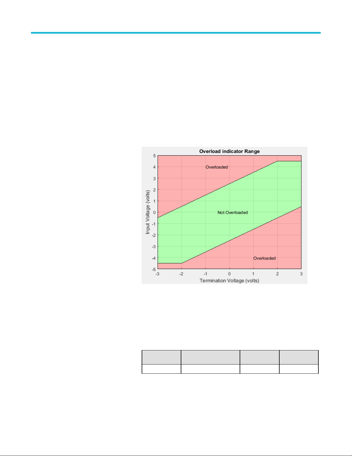
Overload indicator range, typical
(P77C292MM tip only)
CMMR/DMRR, typical, unfiltered, probe only
The Overload indicator is active when the probe input is current limited or when an
input overvoltage condition is detected.
DC-50 MHz 34 dB
50 MHz-800 MHz 24 dB
800 MHz-4 GHz 14 dB
4 GHz-10 GHz 10 dB
Channel isolation, typical Unfiltered, probe only
DC-50 MHz
>40 dB >30 dB >15 dB >6 dB
Time delay, typical 5.05 ns ± 0.1 ns
Small signal rise time, typical
TDP7700 Series TriMode™ Probes Technical Reference 23
50 MHz-800 MHz 800 MHz-4 GHz 4 GHz-8 GHz
Page 32

Specifications
10% - 90% Rise Time
20% - 80% Rise Time
Small signal frequency response,
typical
System noise, 10 mvV/div, probe with P77STCABL tip
Probe Rise time
TDP7710 <45 ps
TDP7708 <55 ps
TDP7706 <65 ps
TDP7704 <100 ps
Probe Rise time
TDP7710 <32 ps
TDP7708 <38 ps
TDP7706 <46 ps
TDP7704 <72 ps
Probe Frequency response
TDP7710 ≥10 GHz
TDP7708 ≥8 GHz
TDP7706 ≥6 GHz
TDP7704 ≥4 GHz
System Noise
System Noise, Typical
DC input resistance ( , typical)
Low frequency input capacitance (differential, typical)
Probe A, B mode C mode D mode
TDP7710 < 4.65 mV RMS < 4.65 mV RMS < 4.65 mV RMS
TDP7708 < 4.65 mV RMS < 4.65 mV RMS < 4.65 mV RMS
TDP7706 < 4.1 mV RMS < 4.1 mV RMS < 4.1 mV RMS
TDP7704 < 4.1 mV RMS < 4.1 mV RMS < 4.1 mV RMS
Probe A, B mode C mode D mode
TDP7710 < 3.6 mV RMS < 2.8 mV RMS < 3.9 mV RMS
TDP7708 < 3.3 mV RMS < 2.6 mV RMS < 3.8 mV RMS
TDP7706 < 3.0 mV RMS < 2.5 mV RMS < 3.7 mV RMS
TDP7704 < 2.7 mV RMS < 2.3 mV RMS < 3.2 mV RMS
Tips/Adapters Differential
P77C292MM
P77STFLXA, P77STCABL
P77BRWSR
100 Ω
100 kΩ
144 kΩ ± 20%
Solder-in tips 0.4 pF
Browser 0.23 pF @ 50 mil spacing
0.22 pF @ 200 mil spacing
TDP7700 Series TriMode™ Probes Technical Reference 24
Page 33

Operating voltage window, typical
Solder-in tips ±5.25 V
Browser ±10 V
SMA adapter ±4 V
Offset voltage range, typical
Solder-in tips -4 V to +4 V
Browser -10 V to +10 V
SMA adapter -4 V to +4 V
Input range, typical
Specifications
Solder-in tips
Browser
SMA adapter
Impedance graphs
Single-ended Differential
2.5 V
pp
5.0 V
pp
Single-ended Differential
6.0 V
pp
12.0 V
pp
Single-ended Differential
1.2 V
pp
2.0 V
pp
Figure 27: P77STCABL differential impedance
TDP7700 Series TriMode™ Probes Technical Reference 25
Page 34

Figure 28: P77STCABL SE impedance
Specifications
Figure 29: P77STFLXA differential impedance
Figure 30: PST77FLXA SE impedance
TDP7700 Series TriMode™ Probes Technical Reference 26
Page 35

Figure 31: P77BRWSR differential impedance
Nominal characteristics
Specifications
Weight
Probe cable and head 3.5 oz
Probe (comp box, cable,
head)
Cable length 1.21 m (4.0 feet)
Oscilloscope interface FlexChannel
Accessory connector TekFlex
Environmental
Temperature range
Compensation box and
browser
Cable and solder-in tips Operating: -35 °C to 85 °C (-31 °F to 185 °F)
SMA adapter Operating: -35 °C to 85 °C (-31 °F to 185 °F)
9.6 oz
Operating: 0 °C to +50 °C (32 °F to 122 °F)
Non-Operating: -20 °C to +60 °C (-4 °F to 140 °F)
Non-Operating: -35 °C to 85 °C (-31 °F to 185 °F)
Non-Operating: -35 °C to 85 °C (-31 °F to 185 °F)
Altitude non-operating 12,000 meters
Humidity, comp box
Operating 5% to 90% relative humidity (% RH) at up to +40 °C, 5% to 55% RH above
+40 °C up to +50 °C, non-condensing.
TDP7700 Series TriMode™ Probes Technical Reference 27
Page 36

Specifications
Nonoperating 5% to 90% RH (Relative Humidity) at up to +40 °C, 5% to 55% RH above +40
°C up to +60 °C, non-condensing.
TDP7700 Series TriMode™ Probes Technical Reference 28
Page 37

Performance verification
Test record
Test record for TDP7700.
Model Serial # Procedure performed by Date
System noise
Performance checks
Performance verification
Noise
P77STCABL or
P77STFLXA
Check system noise
This test checks the system noise.
This test is valid when used on an MSO6 Series instrument. Use the following steps to check the system noise:
1. Plug a P77STCABL or P77STFLXA into the probe tip and connect the probe to a channel on the oscilloscope. The LED
on the tip should light up after loading.
2. Set the probe to Differential (A-B) mode.
3. Adjust the vertical resolution so the noise is on the screen and isn't clipping, but still takes up as much of the screen as
possible.
4. Adjust the horizontal scale to 4 μs/division.
5. Add an AC RMS measurement for the channel the probe is plugged into:
a. Tap the Add New... Measure button.
Probe
TDP7710 4 μs/div ≤ 4.65 mV
TDP7708
TDP7706
TDP7704
Horizontal scale Limit Test result
4 μs/div ≤ 4.65 mV
4 μs/div ≤ 4.1 mV
4 μs/div ≤ 4.1 mV
rms
rms
rms
rms
b. Tap the Amplitude Measurements panel.
c. Double-tap the AC RMS measurement to add the measurement badge to the Results bar.
d. Tap outside the menu to close it.
6. Record this measurement in the test record, it should be lower than the system noise specification.
TDP7700 Series TriMode™ Probes Technical Reference 29
Page 38

Index
C
cable assembly 2
channel isolation 22
check noise 29
CMRR
assessing CMRR error 21
common-mode rejection ratio 20
comp box 1
correction filtering 14
D
differential measurements 20
Differential-Mode rejection ratio 21
DMRR 21
DSP correction filtering 14
E
error conditions
LED indicators 2
I
input network 18
input voltage 9
T
TekFlex connector 2
TekVPI interface 4
TriMode operation 7
W
wire length
solder-in tip connection 14
L
LED indicators 2
O
offset voltage 10
operating voltage window 12
operating voltages 8
P
Performance Verification
test record 29
probe components 1
S
skew
defined 19
|
 Loading...