

Page 1
SERVICE MANUAL
19″ COLOR LCD TELEVISION
LC195SL9 B
Page 2

IMPORTANT SAFETY NOTICE
Proper service and repair is important to the safe, reliable operation of all
Funai Equipment. The service procedures recommended by Funai and
described in this service manual are effective methods of performing
service operations. Some of these service special tools should be used
when and as recommended.
It is important to note that this service manual contains various CAUTIONS
and NOTICES which should be carefully read in order to minimize the risk
of personal injury to service personnel. The possibility exists that improper
service methods may damage the equipment. It also is important to
understand that these CAUTIONS and NOTICES ARE NOT EXHAUSTIVE.
Funai could not possibly know, evaluate and advice the service trade of all
conceivable ways in which service might be done or of the possible
hazardous consequences of each way. Consequently, Funai has not
undertaken any such broad evaluation. Accordingly, a servicer who uses a
service procedure or tool which is not recommended by Funai must first
use all precautions thoroughly so that neither his safety nor the safe
operation of the equipment will be jeopardized by the service method
selected.
TABLE OF CONTENTS
Specifications . . . . . . . . . . . . . . . . . . . . . . . . . . . . . . . . . . . . . . . . . . . . . . . . . . . . . . . . . . . . . . . . . . . . . . . . . . . 1-1
Important Safety Precautions . . . . . . . . . . . . . . . . . . . . . . . . . . . . . . . . . . . . . . . . . . . . . . . . . . . . . . . . . . . . . . . 2-1
Standard Notes for Servicing . . . . . . . . . . . . . . . . . . . . . . . . . . . . . . . . . . . . . . . . . . . . . . . . . . . . . . . . . . . . . . . 3-1
Cabinet Disassembly Instructions. . . . . . . . . . . . . . . . . . . . . . . . . . . . . . . . . . . . . . . . . . . . . . . . . . . . . . . . . . . . 4-1
Electrical Adjustment Instructions . . . . . . . . . . . . . . . . . . . . . . . . . . . . . . . . . . . . . . . . . . . . . . . . . . . . . . . . . . . . 5-1
How to initialize the LCD Television . . . . . . . . . . . . . . . . . . . . . . . . . . . . . . . . . . . . . . . . . . . . . . . . . . . . . . . . . . 6-1
Block Diagrams . . . . . . . . . . . . . . . . . . . . . . . . . . . . . . . . . . . . . . . . . . . . . . . . . . . . . . . . . . . . . . . . . . . . . . . . . . 7-1
Schematic Diagrams / CBA’s and Test Points. . . . . . . . . . . . . . . . . . . . . . . . . . . . . . . . . . . . . . . . . . . . . . . . . . . 8-1
Waveforms . . . . . . . . . . . . . . . . . . . . . . . . . . . . . . . . . . . . . . . . . . . . . . . . . . . . . . . . . . . . . . . . . . . . . . . . . . . . . 9-1
Wiring Diagram . . . . . . . . . . . . . . . . . . . . . . . . . . . . . . . . . . . . . . . . . . . . . . . . . . . . . . . . . . . . . . . . . . . . . . . . . 10-1
Exploded Views. . . . . . . . . . . . . . . . . . . . . . . . . . . . . . . . . . . . . . . . . . . . . . . . . . . . . . . . . . . . . . . . . . . . . . . . . 11-1
Mechanical Parts List . . . . . . . . . . . . . . . . . . . . . . . . . . . . . . . . . . . . . . . . . . . . . . . . . . . . . . . . . . . . . . . . . . . . 12-1
Electrical Parts List . . . . . . . . . . . . . . . . . . . . . . . . . . . . . . . . . . . . . . . . . . . . . . . . . . . . . . . . . . . . . . . . . . . . . . 13-1
The LCD panel is manufactured to provide many years of useful life.
Occasionally a few non active pixels may appear as a tiny spec of color.
This is not to be considered a defect in the LCD screen.
Page 3
SPECIFICATIONS
< TUNER / NTSC >
ANT. Input ---------------------- 75 Ω Unbal., F type
Description Condition Unit Nominal Limit
1. AFT Pull-In Range --- MHz ±2.3 ±2.1
20
20
23
2. Syncronizing Sens.
TV.ch.4
CA.ch.31
CA.ch.87
dBµ
dBµ
dBµ
---
---
---
< TUNER / ATSC >
Description Condition Unit Nominal Limit
1. Received Freq. Range (-28dBm) --- kHz --- ±100
2. ATSC Dynamic Range (min / max)
ch.4
ch.10
ch.41
dBm
dBm
dBm
---
---
---
-76/0
-76/0
-74/+4
< LCD PANEL >
Description Condition Unit Nominal Limit
1. Native Pixel Resolusion
2. Brightness (w / filter) --- cd/m
3. Viewing Angle
Horizontal
Vert ical
Horizontal
Vert ical
pixels
pixels
°
°
1440
900
2
220 ---
-85 to 85
-80 to 80
---
---
---
---
< VIDEO >
Description Condition Unit Nominal Limit
1. Over Scan
2. Color Temperature
3. Resolution (composite video)
Horizontal
Vert ical
--x
y
Horizontal
Vert ical
%
%
°K 12000
line
line
6
6
0.272
0.278
270
350
6±5
6±5
--±3%
±3%
---
---
1-1 A8AN4SP
Page 4

< AUDIO >
All items are measured across 8 Ω load at speaker output terminal with L.P.F. / Video1 Input.
Description Condition Unit Nominal Limit
1. Audio Output Power
2. Audio Distortion 500mW: Lch/Rch % 1.5/1.5 3.0/3.0
3. Audio Freq. Response (NTSC)
Note: Nominal specifications represent the design specifications. All units should be able to approximate these.
Some will exceed and some may drop slightly below these specifications. Limit specifications represent
the absolute worst condition that still might be considered acceptable. In no case should a unit fail to meet
limit specifications.
-6dB/10% THD:
Lch/Rch
-
6dB: Lch
-
6dB: Rch
W 1.0/1.0 0.8/0.8
Hz
Hz
70 to 10 k
70 to 10 k
---
---
1-2 A8AN4SP
Page 5
IMPORTANT SAFETY PRECAUTIONS
Prior to shipment from the factory, our products are strictly inspected for recognized product safety and electrical
codes of the countries in which they are to be sold. However, in order to maintain such compliance, it is equally
important to implement the following precautions when a set is being serviced.
Safety Precautions for LCD TV
Circuit
1. Before returning an instrument to the
customer, always make a safety check of the
entire instrument, including, but not limited to, the
following items:
a. Be sure that no built-in protective devices are
defective and have been defeated during
servicing. (1) Protective shields are provided
on this chassis to protect both the technician
and the customer. Correctly replace all missing
protective shields, including any removed for
servicing convenience. (2) When reinstalling
the chassis and/or other assembly in the
cabinet, be sure to put back in place all
protective devices, including but not limited to,
nonmetallic control knobs, insulating
fishpapers, adjustment and compartment
covers/shields, and isolation resistor/capacitor
networks. Do not operate this instrument or
permit it to be operated without all
protective devices correctly installed and
functioning. Servicers who defeat safety
features or fail to perform safety checks
may be liable for any resulting damage.
b. Be sure that there are no cabinet openings
through which an adult or child might be able to
insert their fingers and contact a hazardous
voltage. Such openings include, but are not
limited to, (1) spacing between the Liquid
Crystal Panel and the cabinet mask, (2)
excessively wide cabinet ventilation slots, and
(3) an improperly fitted and/or incorrectly
secured cabinet back cover.
c. Antenna Cold Check - With the instrument AC
plug removed from any AC source, connect an
electrical jumper across the two AC plug
prongs. Place the instrument AC switch in the
on position. Connect one lead of an ohmmeter
to the AC plug prongs tied together and touch
the other ohmmeter lead in turn to each tuner
antenna input exposed terminal screw and, if
applicable, to the coaxial connector. If the
measured resistance is less than 1.0 megohm
or greater than 5.2 megohm, an abnormality
exists that must be corrected before the
instrument is returned to the customer. Repeat
this test with the instrument AC switch in the off
position.
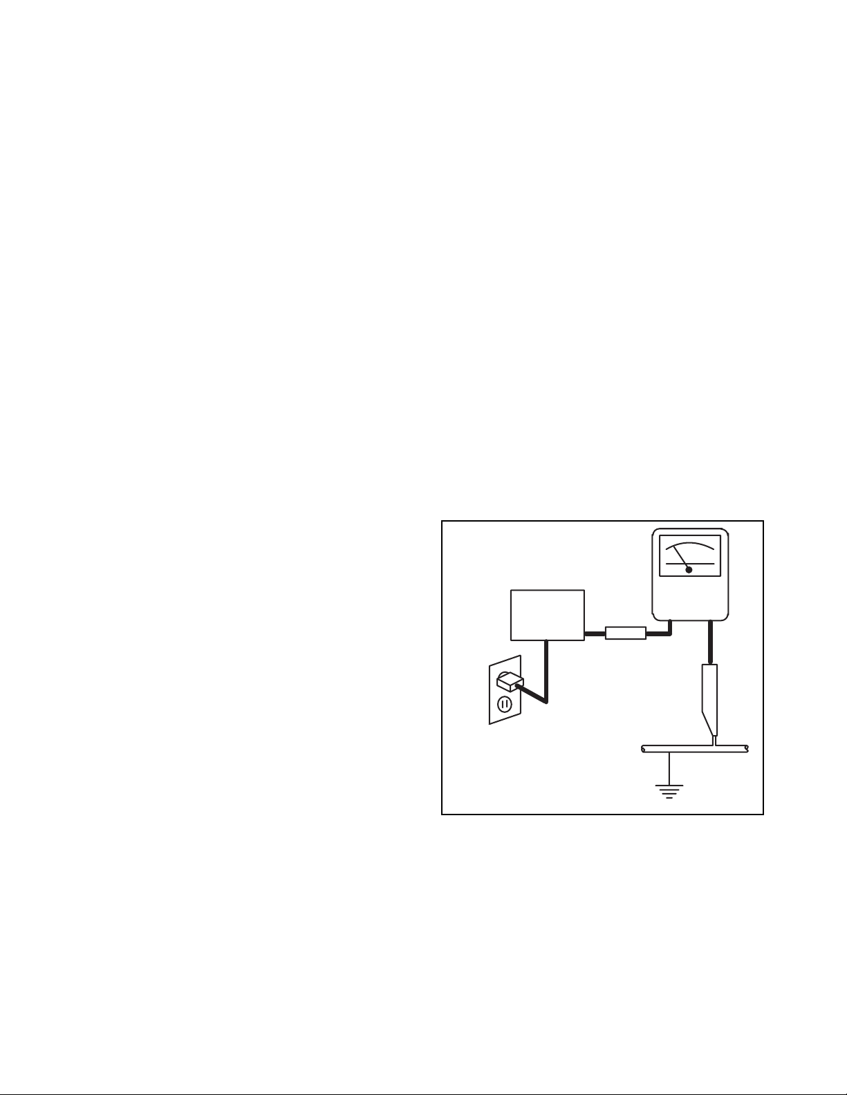
d. Leakage Current Hot Check - With the
instrument completely reassembled, plug the
AC line cord directly into a 120 V AC outlet. (Do
not use an isolation transformer during this
test.) Use a leakage current tester or a
metering system that complies with American
National Standards Institute (ANSI) C101.1
Leakage Current for Appliances and
Underwriters Laboratories (UL) 1410, (50.7).
With the instrument AC switch first in the on
position and then in the off position, measure
from a known earth ground (metal water pipe,
conduit, etc.) to all exposed metal parts of the
instrument (antennas, handle brackets, metal
cabinet, screw heads, metallic overlays, control
shafts, etc.), especially any exposed metal
parts that offer an electrical return path to the
chassis. Any current measured must not
exceed 0.5 milli-ampere. Reverse the
instrument power cord plug in the outlet and
repeat the test.
READING SHOULD
NOT BE ABOVE 0.5 mA
LEAKAGE
DEVICE
BEING
TESTED
TEST ALL EXPOSED
METAL SURFACES
ALSO TEST WITH
PLUG REVERSED
USING AC
ADAPTER PLUG
AS REQUIRED
ANY MEASUREMENTS NOT WITHIN THE
LIMITS SPECIFIED HEREIN INDICATE A
POTENTIAL SHOCK HAZARD THAT MUST
BE ELIMINATED BEFORE RETURNING THE
INSTRUMENT TO THE CUSTOMER OR
BEFORE CONNECTING THE ANTENNA OR
ACCESSORIES.
2. Read and comply with all caution and safety-
related notes on or inside the receiver cabinet, on
the receiver chassis, or on the Liquid Crystal
Panel.
CURRENT
TESTER
+
EARTH
GROUND
_
2-1 LTVN_ISP
Page 6

3. Design Alteration Warning - Do not alter or add
to the mechanical or electrical design of this TV
receiver. Design alterations and additions,
including, but not limited to circuit modifications
and the addition of items such as auxiliary audio
and/or video output connections, might alter the
safety characteristics of this receiver and create a
hazard to the user. Any design alterations or
additions will void the manufacturer's warranty and
may make you, the servicer, responsible for
personal injury or property damage resulting
therefrom.
4. Hot Chassis Warning a. Some TV receiver chassis are electrically
connected directly to one conductor of the AC
power cord and maybe safety-serviced without
an isolation transformer only if the AC power
plug is inserted so that the chassis is
connected to the ground side of the AC power
source. To confirm that the AC power plug is
inserted correctly, with an AC voltmeter,
measure between the chassis and a known
earth ground. If a voltage reading in excess of
1.0 V is obtained, remove and reinsert the AC
power plug in the opposite polarity and again
measure the voltage potential between the
chassis and a known earth ground.
b. Some TV receiver chassis normally have 85V
AC(RMS) between chassis and earth ground
regardless of the AC plug polarity. This chassis
can be safety-serviced only with an isolation
transformer inserted in the power line between
the receiver and the AC power source, for both
personnel and test equipment protection.
c. Some TV receiver chassis have a secondary
ground system in addition to the main chassis
ground. This secondary ground system is not
isolated from the AC power line. The two
ground systems are electrically separated by
insulation material that must not be defeated or
altered.
5. Observe original lead dress. Take extra care to
assure correct lead dress in the following areas: a.
near sharp edges, b. near thermally hot parts-be
sure that leads and components do not touch
thermally hot parts, c. the AC supply, d. high
voltage, and, e. antenna wiring. Always inspect in
all areas for pinched, out of place, or frayed wiring.
Check AC power cord for damage.
6. Components, parts, and/or wiring that appear to
have overheated or are otherwise damaged
should be replaced with components, parts, or
wiring that meet original specifications.
Additionally, determine the cause of overheating
and/or damage and, if necessary, take corrective
action to remove any potential safety hazard.
7. Product Safety Notice - Some electrical and
mechanical parts have special safety-related
characteristics which are often not evident from
visual inspection, nor can the protection they give
necessarily be obtained by replacing them with
components rated for higher voltage, wattage, etc.
Parts that have special safety characteristics are
identified by a # on schematics and in parts lists.
Use of a substitute replacement that does not
have the same safety characteristics as the
recommended replacement part might create
shock, fire, and/or other hazards. The product's
safety is under review continuously and new
instructions are issued whenever appropriate.
Prior to shipment from the factory, our products
are strictly inspected to confirm they comply with
the recognized product safety and electrical codes
of the countries in which they are to be sold.
However, in order to maintain such compliance, it
is equally important to implement the following
precautions when a set is being serviced.
2-2 LTVN_ISP
Page 7

Precautions during Servicing
A. Parts identified by the # symbol are critical for
safety.
Replace only with part number specified.
B. In addition to safety, other parts and assemblies
are specified for conformance with regulations
applying to spurious radiation. These must also be
replaced only with specified replacements.
Examples: RF converters, RF cables, noise
blocking capacitors, and noise blocking filters, etc.
C. Use specified internal wiring. Note especially:
1) Wires covered with PVC tubing
2) Double insulated wires
3) High voltage leads
D. Use specified insulating materials for hazardous
live parts. Note especially:
1) Insulation Tape
2) PVC tubing
3) Spacers
4) Insulators for transistors.
E. When replacing AC primary side components
(transformers, power cord, etc.), wrap ends of
wires securely about the terminals before
soldering.
F. Observe that the wires do not contact heat
producing parts (heat sinks, oxide metal film
resistors, fusible resistors, etc.)
G. Check that replaced wires do not contact sharp
edged or pointed parts.
H. When a power cord has been replaced, check that
5~6 kg of force in any direction will not loosen it.
I. Also check areas surrounding repaired locations.
J. Use care that foreign objects (screws, solder
droplets, etc.) do not remain inside the set.
K. When connecting or disconnecting the internal
connectors, first, disconnect the AC plug from the
AC supply outlet.
L. When installing parts or assembling the cabinet
parts, be sure to use the proper screws and
tighten certainly.
2-3 LTVN_ISP
Page 8
Safety Check after Servicing
Examine the area surrounding the repaired location for damage or deterioration. Observe that screws, parts and
wires have been returned to original positions. Afterwards, perform the following tests and confirm the specified
values in order to verify compliance with safety standards.
1. Clearance Distance
When replacing primary circuit components, confirm
specified clearance distance (d) and (d') between
soldered terminals, and between terminals and
surrounding metallic parts. (See Fig. 1)
Table 1: Ratings for selected area
Chassis or Secondary Conductor
Primary Circuit
AC Line Voltage Region
110 to 130 V
Note: This table is unofficial and for reference only. Be
sure to confirm the precise values.
U.S.A. or
Canada
Clearance
Distance (d), (d’)
≥ 3.2 mm
(0.126 inches)
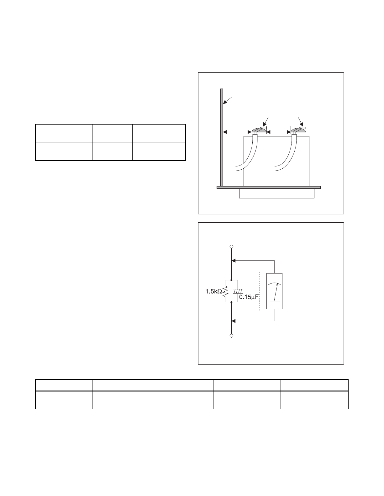
2. Leakage Current Test
Confirm the specified (or lower) leakage current
between B (earth ground, power cord plug prongs) and
externally exposed accessible parts (RF terminals,
antenna terminals, video and audio input and output
terminals, microphone jacks, earphone jacks, etc.) is
lower than or equal to the specified value in the table
below.
Measuring Method: (Power ON)
Insert load Z between B (earth ground, power cord plug
prongs) and exposed accessible parts. Use an AC
voltmeter to measure across both terminals of load Z.
See Fig. 2 and following table.
d' d
Fig. 1
Exposed Accessible Part
Z
AC Voltmeter
(High Impedance)
Earth Ground
B
Power Cord Plug Prongs
Fig. 2
Table 2: Leakage current ratings for selected areas
AC Line Voltage Region Load Z Leakage Current (i) Earth Ground (B) to:
110 to 130 V
Note: This table is unofficial and for reference only. Be sure to confirm the precise values.
U.S.A. or
Canada
0.15 µF CAP. & 1.5 kΩ
RES. Connected in parallel
2-4 LTVN_ISP
i ≤ 0.5 mA rms
Exposed accessible
parts
Page 9
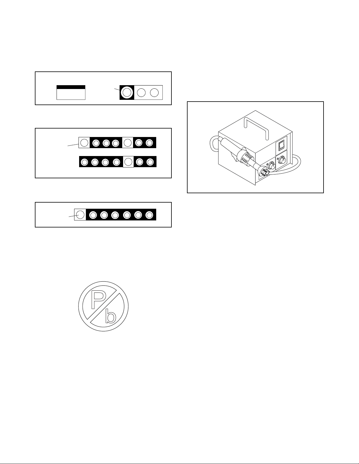
STANDARD NOTES FOR SERVICING
Circuit Board Indications
1. The output pin of the 3 pin Regulator ICs is
indicated as shown.
Top View
Out
2. For other ICs, pin 1 and every fifth pin are
indicated as shown.
Pin 1
3. The 1st pin of every male connector is indicated as
shown.
Pin 1
Input
In
Bottom View
5
10
Pb (Lead) Free Solder
Pb free mark will be found on PCBs which use Pb
free solder. (Refer to figure.) For PCBs with Pb free
mark, be sure to use Pb free solder. For PCBs
without Pb free mark, use standard solder.
Pb free mark
How to Remove / Install Flat Pack-IC
1. Removal
With Hot-Air Flat Pack-IC Desoldering Machine:
1. Prepare the hot-air flat pack-IC desoldering
machine, then apply hot air to the Flat Pack-IC
(about 5 to 6 seconds). (Fig. S-1-1)
Fig. S-1-1
2. Remove the flat pack-IC with tweezers while
applying the hot air.
3. Bottom of the flat pack-IC is fixed with glue to the
CBA; when removing entire flat pack-IC, first apply
soldering iron to center of the flat pack-IC and heat
up. Then remove (glue will be melted). (Fig. S-1-6)
4. Release the flat pack-IC from the CBA using
tweezers. (Fig. S-1-6)
CAUTION:
1. The Flat Pack-IC shape may differ by models. Use
an appropriate hot-air flat pack-IC desoldering
machine, whose shape matches that of the Flat
Pack-IC.
2. Do not supply hot air to the chip parts around the
flat pack-IC for over 6 seconds because damage
to the chip parts may occur. Put masking tape
around the flat pack-IC to protect other parts from
damage. (Fig. S-1-2)
3-1 TVN_SN
Page 10
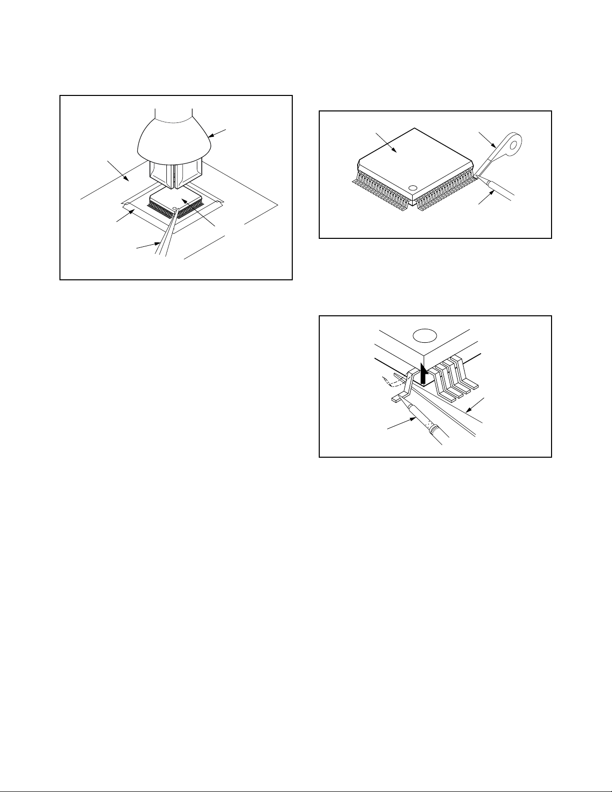
3. The flat pack-IC on the CBA is affixed with glue, so
be careful not to break or damage the foil of each
pin or the solder lands under the IC when
removing it.
With Soldering Iron:
1. Using desoldering braid, remove the solder from
all pins of the flat pack-IC. When you use solder
flux which is applied to all pins of the flat pack-IC,
you can remove it easily. (Fig. S-1-3)
CBA
Masking
Tape
Tweezers
Hot-air
Flat Pack-IC
Desoldering
Machine
Flat Pack-IC
Fig. S-1-2
Flat Pack-IC
Desoldering Braid
Soldering Iron
Fig. S-1-3
2. Lift each lead of the flat pack-IC upward one by
one, using a sharp pin or wire to which solder will
not adhere (iron wire). When heating the pins, use
a fine tip soldering iron or a hot air desoldering
machine. (Fig. S-1-4)
Sharp
Pin
Fine Tip
Soldering Iron
3. Bottom of the flat pack-IC is fixed with glue to the
CBA; when removing entire flat pack-IC, first apply
soldering iron to center of the flat pack-IC and heat
up. Then remove (glue will be melted). (Fig. S-1-6)
4. Release the flat pack-IC from the CBA using
tweezers. (Fig. S-1-6)
Fig. S-1-4
3-2 TVN_SN
Page 11
With Iron Wire:
1. Using desoldering braid, remove the solder from
all pins of the flat pack-IC. When you use solder
flux which is applied to all pins of the flat pack-IC,
you can remove it easily. (Fig. S-1-3)
2. Affix the wire to a workbench or solid mounting
point, as shown in Fig. S-1-5.
3. While heating the pins using a fine tip soldering
iron or hot air blower, pull up the wire as the solder
melts so as to lift the IC leads from the CBA
contact pads as shown in Fig. S-1-5.
4. Bottom of the flat pack-IC is fixed with glue to the
CBA; when removing entire flat pack-IC, first apply
soldering iron to center of the flat pack-IC and heat
up. Then remove (glue will be melted). (Fig. S-1-6)
5. Release the flat pack-IC from the CBA using
tweezers. (Fig. S-1-6)
Note: When using a soldering iron, care must be
taken to ensure that the flat pack-IC is not
being held by glue. When the flat pack-IC is
removed from the CBA, handle it gently
because it may be damaged if force is applied.
Hot Air Blower
2. Installation
1. Using desoldering braid, remove the solder from
the foil of each pin of the flat pack-IC on the CBA
so you can install a replacement flat pack-IC more
easily.
2. The “●” mark on the flat pack-IC indicates pin 1.
(See Fig. S-1-7.) Be sure this mark matches the 1
on the PCB when positioning for installation. Then
presolder the four corners of the flat pack-IC. (See
Fig. S-1-8.)
3. Solder all pins of the flat pack-IC. Be sure that
none of the pins have solder bridges.
Example :
Pin 1 of the Flat Pack-IC
is indicated by a " " mark.
Fig. S-1-7
To Solid
Mounting Point
CBA
Tweezers
Iron Wire
Soldering Iron
Fig. S-1-5
Fine Tip
Soldering Iron
Flat Pack-IC
or
Presolder
Flat Pack-IC
CBA
Fig. S-1-8
Fig. S-1-6
3-3 TVN_SN
Page 12

Instructions for Handling Semiconductors
Electrostatic breakdown of the semi-conductors may
occur due to a potential difference caused by
electrostatic charge during unpacking or repair work.
1. Ground for Human Body
Be sure to wear a grounding band (1 MΩ) that is
properly grounded to remove any static electricity that
may be charged on the body.
2. Ground for Workbench
Be sure to place a conductive sheet or copper plate
with proper grounding (1 MΩ) on the workbench or
other surface, where the semi-conductors are to be
placed. Because the static electricity charge on
clothing will not escape through the body grounding
band, be careful to avoid contacting semi-conductors
with your clothing.
<Incorrect>
<Correct>
1MΩ
CBA
Grounding Band
1MΩ
CBA
Conductive Sheet or
Copper Plate
3-4 TVN_SN
Page 13
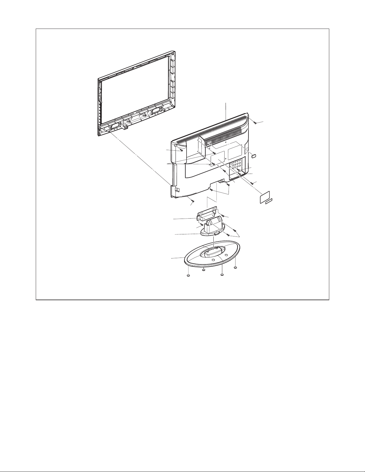
CABINET DISASSEMBLY INSTRUCTIONS
1. Disassembly Flowchart
This flowchart indicates the disassembly steps for the
cabinet parts, and the CBA in order to gain access to
item(s) to be serviced. When reassembling, follow the
steps in reverse order. Bend, route and dress the
cables as they were.
[14] Speaker(s)
[11] IR Sensor CBA
[12] Function CBA
[4] Rear Cabinet
[5] Shield Box
[6] Digital Main
CBA Unit
[7] Tuner Holder
[8] Power Supply
CBA
[9] Junction CBA
[10] Inverter CBA
[13] LCD Module
Assembly
[15] Front Cabinet
[1] Stand Cover
[2] Stand Neck
[3] Fix Stand Holder
2. Disassembly Method
Removal
Step/
Loc.
Part
No.
Stand
[1]
Cover
[2] Stand Neck D1 2(S-2) ---
Fix Stand
[3]
Holder
Rear
[4]
Cabinet
Remove/*Unhook/
Fig.
No.
Unlock/Release/
Unplug/Unclamp/
Note
Desolder
D1 2(S-1) ---
D1 2(S-3) ---
D1 5(S-4), 4(S-5) ---
Removal
Step/
Loc.
No.
Part
Remove/*Unhook/
Fig.
No.
Unlock/Release/
Unplug/Unclamp/
Note
Desolder
2(S-6), 4(S-7), 4(S-8),
[5] Shield Box
*CN3601, *CN3701,
D3
*CN3704, *CN4501,
---
D2
*CN4502
Digital Main
[6]
CBA UnitD2D3
Tuner
[7]
Holder
Power
[8]
Supply
CBA
Junction
[9]
CBA
Inverter
[10]
CBA
IR Sensor
[11]
CBA
Function
[12]
CBA
--------------- ---
D2 (S-9) ---
D2D33(S-10), *CN102,
*CN306, *CN309
D2
*CN403B ---
D3
D2D34(S-11), *CN401,
*CN402, *CN451
D2
*CL101B ---
D3
D2
--------------- ---
D3
---
---
LCD
[13]
Module
D2 --------------- ---
Assembly
[14] Speaker(s) D2 4(S-12) ---
Front
[15]
↓
(1)
Cabinet
↓
(2)
D2 --------------- ---
↓
(3)
↓
(4)
↓
(5)
Note:
(1) Order of steps in procedure. When reassembling,
follow the steps in reverse order. These numbers
are also used as the Identification (location) No. of
parts in figures.
(2) Parts to be removed or installed.
(3) Fig. No. showing procedure of part location
(4) Identification of parts to be removed, unhooked,
unlocked, released, unplugged, unclamped, or
desoldered.
N = Nut, L = Locking Tab, S = Screw,
CN = Connector
* = Unhook, Unlock, Release, Unplug, or Desolder
e.g. 2(S-2) = two Screws (S-2),
2(L-2) = two Locking Tabs (L-2)
(5) Refer to the following "Reference Notes in the
Table."
4-1 A8AN4DC
Page 14
(S-4)
[4] Rear Cabinet
(S-4)
(S-5)
[3] Fix Stand Holder
[2] Stand Neck
[1] Stand Cover
(S-4)
(S-3)
(S-1)
(S-5)
(S-3)
(S-4)
(S-5)
(S-4)
(S-2)
Fig. D1
4-2 A8AN4DC
Page 15
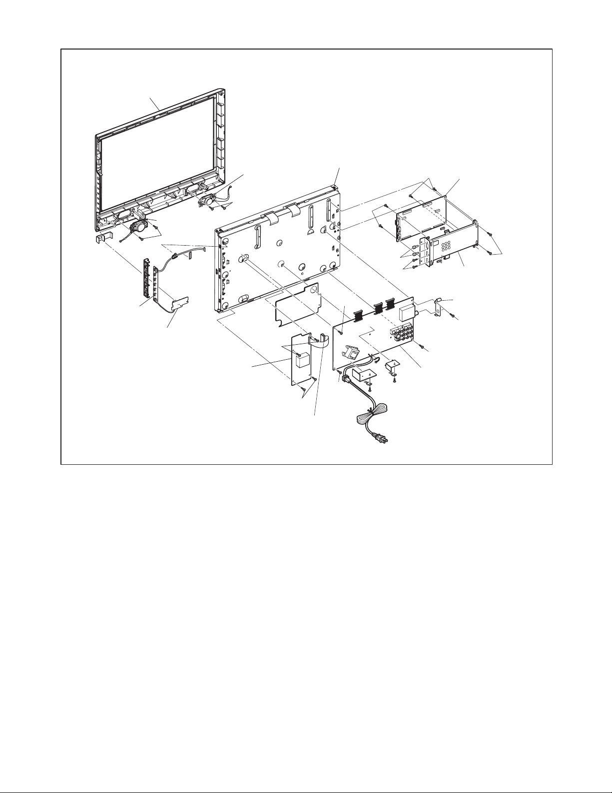
[15] Front Cabinet
[14] Speaker
(S-12)
[14] Speaker
(S-12)
[13] LCD Module
Assembly
(S-8)
(S-8)
[6] Digital Main
CBA Unit
[12] Function
CBA
[11] IR Sensor
CBA
[10] Inverter CBA
(S-11)
(S-10)
(S-11)
[9] Junction CBA
(S-10)
(S-6)
(S-7)
(S-7)
[5] Shield Box
[7] Tuner Holder
(S-9)
(S-10)
[8] Power Supply CBA
Fig. D2
4-3 A8AN4DC
Page 16
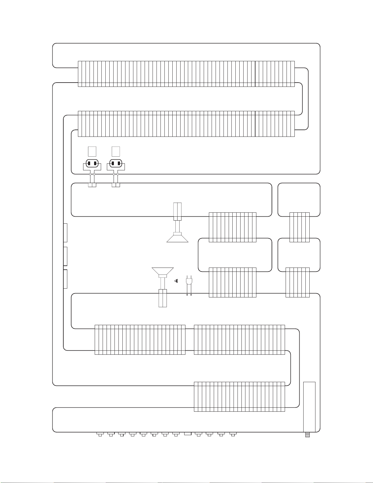
TV Cable Wiring Diagram
To LCD Module
Assembly
Inverter CBA
CN401
Junction
CBA
CL403
To LCD Module
Assembly
To Speaker
CL102
CN402
Function
CBA
CN403B
CN451
CN102
CN309
CN403A
CN301
CN4501 CN4502
CN3601 CN3701
CN302
CN303
Digital Main
CBA Unit
CN3704
Power Supply CBA
CL101A
IR Sensor CBA
CL101B
CN306
To Speaker
Fig. D3
4-4 A8AN4DC
Page 17
ELECTRICAL ADJUSTMENT INSTRUCTIONS
General Note: “CBA” is abbreviation for
“Circuit Board Assembly.”
Note: Electrical adjustments are required after
replacing circuit components and certain
mechanical parts. It is important to perform
these adjustments only after all repairs and
replacements have been completed.
Also, do not attempt these adjustments unless
the proper equipment is available.
Test Equipment Required
1. DC Voltmeter
2. NTSC Pattern Generator (Color Bar W/White
Window, Red Color, Dot Pattern, Gray Scale,
Monoscope, Multi-Burst)
3. Remote control unit
4. Color Analyzer
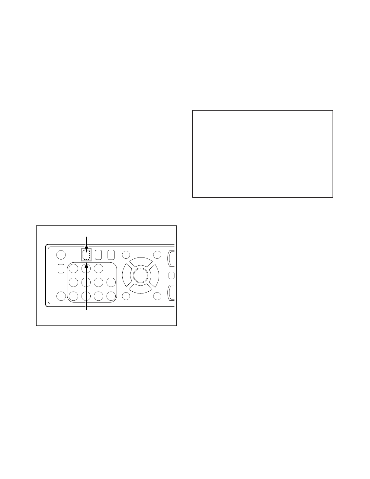
How to make the Service remote
control unit:
Cut “A” portion of the attached remote control unit as
shown in Fig. 1.
How to set up the service mode:
Service mode:
1. Use the service remote control unit.
2. Turn the power on.
3. Press the service button on the service remote
control unit. The following screen appears.
"*" differs depending on the models.
Code :
Boot :
System :
SubCPU :
Pic Code :
Picture :
Other :
Safety :
Tuner :
HDMI1 Block0 :
Block1 :
HDMI2 Block1 :
**********-***
**** * ***
**** * ***
****
**-***-**-****-***
****
**
******-***
*****-*******
**
**
**
service button
A
Fig. 1
5-1 A8AN4EA
Page 18
1. Purity Check Mode
2. VCOM Adjustment.
This mode cycles through full-screen displays of red,
green, blue, and white to check for non-active pixels.
1. Enter the Service mode.
2. Each time pressing [7] button on the service
remote control unit, the display changes as
follows.
Purity Check Mode
White mode
[7] button
[7] button
Black mode
[7] button
Red mode
[7] button
Green mode
Test Point
Screen
Adj. Point
[CH o/p]
buttons
M. EQ. Spec.
Color analyzer
See below
Figure
It carries out in a darkroom.
Perpendicularity
L = 3 cm
Color Analyzer
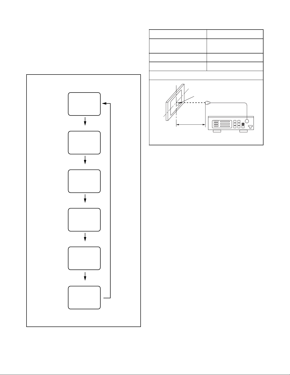
1. Operate the unit for more than 20 minutes.
2. Set the color analyzer and bring the optical
receptor to the center on the LCD-Panel surface
after zero point calibration as shown above.
Note: The optical receptor must be set
perpendicularly to the LCD Panel surface.
3. Enter the Service mode.
4. Press [3] button on the service remote control unit.
5. Press [CH o / p] buttons on the service remote
control unit so that the color analyzer value
becomes minimum.
[7] button
Blue mode
[7] button
White 25% mode
Note:
When entering this mode, the default setting is White mode.
5-2 A8AN4EA
Page 19

The following adjustment normally are not attempted in
the field. Only when replacing the LCD Panel then adjust
as a preparation.
3. White Balance Adjustment
Purpose: To mix red, green and blue beams correctly
for pure white.
Symptom of Misadjustment: White becomes bluish
or reddish.
Test Poi nt
Screen
Adj. Point Mode Input
[CH o/p]
buttons
[VIDEO1]
C/D
M. EQ. Spec.
White Raster
(APL 70%)
or
(APL 25%)
5. [CUTOFF]
Press [3] button to select “COB” for Blue Cutoff
adjustment. Press [1] button to select “COR” for
Red Cutoff adjustment.
[DRIVE]
Press [6] button to select “DB” for Blue Drive
adjustment. Press [4] button to select “DR” for Red
Drive adjustment.
6. In each color mode, press [CH o / p] buttons to
adjust the values of color.
7. Adjust Cutoff and Drive so that the color
temperature becomes 12000°K (x
=
0.272 / y
=
0.278 ±0.005).
Pattern Generator,
Color analyzer
x= 0.272 ± 0.005
y= 0.278 ± 0.005
Figure
It carries out in a darkroom.
Perpendicularity
L = 3 cm
INPUT: WHITE 70%, 25%
Color Analyzer
1. Operate the unit for more than 20 minutes.
2. Input the White Raster(70%=70IRE, 25%=25IRE).
INPUT SIGNAL
25%=25IRE
70%=70IRE
3. Set the color analyzer to the CHROMA mode and
bring the optical receptor to the center on the
LCD-Panel surface after zero point calibration as
shown above.
Note: The optical receptor must be set
perpendicularly to the LCD Panel surface.
4. Enter the Service mode. Press [VOL. n] button on
the service remote control unit and select “C/D”
mode.
5-3 A8AN4EA
Page 20

HOW TO INITIALIZE THE LCD TELEVISION
How to initialize the LCD television:
1. Turn the power on.
2. To enter the service mode, press the service
button on the service remote control unit. (Refer to
page 5-1.)
- To cancel the service mode, press [POWER]
button on the remote control unit.
3. Press [INFO] button on the service remote control
unit to initialize the LCD television.
4. "INITIALIZED" will appear in the upper right of the
screen. "INITIALIZED" color will change to green
from red when initializing is complete.
6-1 A8AN4INT
Page 21

BLOCK DIAGRAMS
System Control Block Diagram
REMOTE
RCV101
+3.3V
D102
STANDBY
D101
SENSOR
CL101B
REMOTE22
CL101A
CL102
REMOTE22
CN102
CN301CN3601
POWER
LED144
P-ON-H155
LED144
P-ON-H155
KEY-IN166
CN302
KEY SWITCH
TO POWER
SUPPLY
BLOCK
DIAGRAM
P-ON-H1
P-ON-H2
IR SENSOR CBA
FUNCTION
CBA
POWER SUPPLY CBA
X3101
4MHz
OSC
6
XOUT
8
XIN
TO
INVERTER
BLOCK
DIAGRAM
PROTECT3
8
CN309
CN301CN3601
BACKLIGHT-SW
9
3
BACKLIGHT-SW
21
(CL403)
TO POWER
SUPPLY
BLOCK
DIAGRAM
RESET
PROTECT1
PROTECT2
POWER SUPPLY CBA
CN302CN3701
PROTECT222 2
PROTECT321 3
PROTECT123 1
RESET20 4
TO DIGITAL
SIGNAL
PROCESS
BLOCK
DIAGRAM
SDA
SCL
IC3102 (MEMORY)
5
6
7 WP
VCOM-PWM
2
19
20
WP
SCL
SDA
21
VCOM-PWM
3
RESET
PROTECT1 22
PROTECT2 23
PROTECT3 4
TO AUDIO-2
BLOCK
DIAGRAM
IC3301
(MAIN MICRO CONTROLLER)
SCL
AE13
CN3704CN303
SCL15 9
14
SCL
REMOTE20 4
P-ON-H1222
P-ON-H2123
SDA
AF13
SDA16 8
15
SDA
KEY-IN123 1
LED111 13
CN3701
(SUB MICRO CONTROLLER)
IC3101
S-SW
S-SW
C3
LED1
12
KEY-IN124
REMOTE
RXD
P-ON-H114
P-ON-H213
11
R22
REMOTE
TXD
15
16RXD1
P22
N22
TXD1
INPUT0
A11
INPUT0
INPUT1
RESET-MAIN
5RESET-MAIN
V24
INPUT1
E12
AMP-MUTE-SUB
18
C12
AMP-MUTE-MAIN
IC3706 (MEMORY)
SPI-CLK
SPI-DO
Y25
Y24
652
SPI-DI
SPI-CLK
SPI-DI
SPI-CS0
W25
W24
1
SPI-DO
SPI-CS0
SPI-CS1SPI-CS1
W26
3
AMP-MUTE
CLKOUT
CLKIN
U25
U26
25MHz
OSC
X3301
B3
BACKLIGHT-SW
DIGITAL MAIN CBA UNIT
TU1 (TUNER UNIT)
POWER SUPPLY CBA
TO VIDEO
BLOCK
DIAGRAM
7-1
TO AUDIO-1
BLOCK
DIAGRAM
A8AN4BLS
Page 22

Video Block Diagram
TO DIGITAL
SIGNAL
AUDIO SIGNAL
PROCESS
BLOCK
DIAGRAM
TO SYSTEM
CONTROL
BLOCK
DIAGRAM
TO DIGITAL
SIGNAL
PROCESS
BLOCK
DIAGRAM
VIDEO SIGNAL
DIGITAL MAIN CBA UNIT
WF1WF2WF3
VIDEO
S-VIDEO-Y
S-VIDEO-C
153108
S-VIDEO-Y19
VIDEO23
CN302 CN3701
COMP-Y
S-VIDEO-C21
COMP-Y14
COMP-Pr
COMP-Pb
7
COMP-Pb16
COMP-Pr17
WF4WF5WF6
S-SW
IF-AGC
DIF-OUT1
DIF-OUT2
IF-AGC18 6
DIF-OUT2
DIF-OUT1
S-SW
123
20 4
22 2
CN303 CN3704
TU-CVBS
TU-CVBS11 13
BUFFER
20
21
18
IF-AGC
DIF-OUT2
DIF-OUT1
Q3
4
VIDEO-OUT
POWER SUPPLY CBA
JK7702
VIDEO-IN1
CY
JK7701
S-VIDEO
-IN1
JK7711
COMPONENT
-Y-IN1
JK7712
COMPONENT
-Pb-IN1
JK7713
COMPONENT
-Pr-IN1
TU1
(TUNER UNIT)
7-2 A8AN4BLV
Page 23

Audio-1 Block Diagram
TO
DIGITAL
SIGNAL
PROCESS
BLOCK
DIAGRAM
TO
SYSTEM
CONTROL
BLOCK
DIAGRAM
TO
DIGITAL
SIGNAL
PROCESS
BLOCK
DIAGRAM
AUDIO SIGNAL
DIGITAL MAIN CBA UNIT
BCLK
IC3702
(AUDIO A/D CONVERTER)
CN3704CN303
WF7
IC7301
(INPUT SELECT)
1
ACLK
LRCLK
AUX-ADATA
111015
12
A/D
CONVERTER
(L-CH)
(R-CH)
1
2
AUDIO(L)321
AUDIO(R)420
3
2
4
5
11
INPUT1
CN3704CN303
13
109
SW CTL
12
14
15
Q7302
Q7301
SIF
INPUT0
INPUT1717
INPUT0816
SIF915
POWER SUPPLY CBA
BUFFER
Q4,Q5
3
JK7704
JK7703
AUDIO(L)
-IN1
AUDIO(R)
-IN1
JK7716
COMPONENT
AUDIO(L)
-IN1
JK7717
COMPONENT
AUDIO(R)
-IN1
JK7705
HDMI
JK7706
AUDIO(L)-IN
7-3
HDMI
AUDIO(R)-IN
JK7501
PC-AUDIO
SIF-OUT
TU1
(TUNER UNIT)
-IN
A8AN4BLA1
Page 24

Audio-2 Block Diagram
SP801
SPEAKER
L-CH
SP802
SPEAKER
R-CH
AUDIO SIGNAL
IC7304 (AUDIO AMP)
IC702
(AMP)
+9V
CN306
11
AMP
(L-CH)
6
3
SP(L) 1
SP-GND 2
215
VOLUME
MUTE
/STANDBY
SP(R) 1
CN451
SP-GND 2
INVERTER CBA
CN403B
14
SP(R)11 11SP(R)11 11
AMP
7
2
CONTROL
(R-CH)
1
7
6
+5V
DIGITAL
JK7715
AUDIO-OUT
(COAXIAL)
CN403ACN309
CL403
JUNCTION
CBA
IC701
(AUDIO D/A CONVERTER)
(L-CH)
8
CN302
LRCLK14 10
CN3701
LRCLK
TO
15
D/A
BCLK15 9
BCLK
DIGITAL
14
(R-CH)
CONVERTER
AD ATA16 8
ACLK
ADATA
SIGNAL
PROCESS
BLOCK
567
ACLK17 7
SPDIF18 6
SPDIF
DIAGRAM
AUDIO MUTE
Q7303
BUFFER
Q7201
AMP-MUTE12 12
AMP-MUTE
TO SYSTEM
CONTROL
BLOCK
DIAGRAM
7-4
POWER SUPPLY CBA
DIGITAL MAIN CBA UNIT
A8AN4BLA2
Page 25

Digital Signal Process Block Diagram
LCD MODULE
ASSEMBLY
BRSB2(+)52
CN4501
AUDIO SIGNAL
757473727170666564
VIDEO SIGNAL
IC4201(LCD DRIVE)
BRSB2(-)51
BRSB1(+)50
BRSB1(-)49
BRSB0(+)48
BRSB0(-)47
BRSG2(+)46
BRSG2(-)45
BRSG1(+)44
BRSG1(-)43
BRSG0(+)42
BRSG0(-)41
BRSR2(+)17
63
62616059585756556968907778
D-RSDS
OUTPUT
LVDS
RX
242522232021161718
AF20
AE20
AD19
AD20
AE19
AF19
AF18
AE18
BRSR2(-)16
AE21
BRSR1(+)15
19
AF21
BRSR1(-)14
BRSR0(+)13
BRSR0(-)12
BRSCLK(+)22
BRSCLK(-)21
V-COM7
STH-S11
TP119
POL18
STV5
81
LVD S
FRSB2(+)53
FRSB2(-)52
FRSB1(+)51
FRSB1(-)50
FRSB0(+)49
FRSB0(-)48
FRSG2(+)47
FRSG2(-)46
FRSG1(+)45
V-COM9
CN4502
52515049484744434140393837363534333246
DATA
MAPPING
TX
FRSG1(-)44
D-RSDS
LVDS
9107856123
AF25
AF24
AE25
AD25
AD26
FRSG0(+)43
FRSG0(-)42
OUTPUT
RX
AE24
AD23
FRSR2(+)18
AD24
FRSR2(-)17
AF26
FRSR1(+)16
4
AE26
FRSR1(-)15
FRSR0(+)14
FRSR0(-)13
FRSCLK(+)23
FRSCLK(-)22
STH-F55
CPV6
OE15
STV7
TP120
POL19
DRIVE
IC4511,Q4511,
145
808284
IC4202 (MEMORY)
SCL
87
6
SCL
(SDRAM)
IC3201
SDA
88
5
SDA
Q4512,Q4513
TO SYSTEM
DATA(0-15)
H1,H3,H7,H9
B1,B9,C2,C8,
F1,F9,G2,G8,
D1,D3,D7,D9,
A13-15,A18,
A21-23,B13-15,
B17,B19-23
C15,C17-19,
VCOM-PWM
CONTROL
BLOCK
DIAGRAM
ADDESS(0-12)
M2,M3,M7,M8,
N2,N3,N7,N8,
P2,P3,P7,P8,R2
C23,C24,D14,
D15,D17-19,
D22,D23
IC3301 (DIGITAL SIGNAL PROCESS)
DIGITAL MAIN CBA UNIT
T4
Y3
TU-CVBS
T3
U4
COMP-Y
COMP-Pb
V4
COMP-Pr
TO VIDEO
BLOCK
DIAGRAM
W3
VIDEO
S-VIDEO-Y
A/D
SW
V3
U3
S-VIDEO-C
CONVERTER
DEMODULATOR
/MPEG DECODER
AF2
AE2
DIF-OUT1
DIF-OUT2
IF-AGC
TO VIDEO
BLOCK
DIAGRAM
IF-AGC
AF7
DEMODULATOR
AF5
DIGITAL
SIGNAL
PROCESS
AUDIO I/F
AF15
AF16
AE15
AE16
AD15
SIF
AUX-ADATA
BCLK
TO AUDIO-1
BLOCK
ACLK
LRCLK
DIAGRAM
SPDIF
AD ATA
AD16
BCLK
TO AUDIO-2
LRCLK
BLOCK
ACLK
DIAGRAM
JK4001
AUDIO
DECODER
A9
B9
C8
TMDS-D0(+)
TMDS-D0(-)
TMDS-D1(+)
79461
B8
A8
C9
TMDS-D1(-)
TMDS-D2(+)
TMDS-D2(-)
3
HDMI-IN1
E9
B10
A10
C10
BUFFER
Q4002
BUFFER
TMDS-CLOCK(+)
TMDS-CLOCK(-)
SDA
SCL
101216
15
VIDEO
DECODER
HDMI
I/F
Q4001
JK4002
A5
B5
C4
TMDS-D0(+)
TMDS-D0(-)
TMDS-D1(+)
TMDS-D1(-)
79461
B4A4B6
C5
TMDS-D2(+)
TMDS-D2(-)
3
HDMI-IN2
A6D7B7
BUFFER
Q4004
BUFFER
TMDS-CLOCK(+)
TMDS-CLOCK(-)
SDA
SCL
101216
15
Q4003
7-5
A8AN4BLD
Page 26
Inverter Block Diagram
BACK
LIGHT
1
2
CN401
BACK
1
CN402
LIGHT
2
LCD MODULE
ASSEMBLY
11
7
2
1
CURRENT
CONTROL
SWITCH
Q408
T401
14
9
13
4
5
10
INVERTER CBA
Q406
SW+22V
OVER CURRENT
PROTECTOR
Q411
Q401
Q402
12
6
8
3
Q405
OVER CURRENT
PROTECTOR
Q412
JS411
Q404
Q410
OVER VOLTAGE
Q403
PROTECTOR
JUNCTION
CBA
2
CN403B
FEEDBACK2
2
CL403 CN403A
FEEDBACK
TO POWER
SUPPLY
1
3,4
INV+22V3,4
+35V1
1
3,4
INV+22V
+35V
BLOCK
DIAGRAM
(CN309)
CN403B
CL403 CN403A
TO SYSTEM
CONTROL
7-6
8
9
PROTECT38
BACKLIGHT-SW
9
8
9
PROTECT3
BACKLIGHT-SW
BLOCK
DIAGRAM
(CN309)
A8AN4BLINV
Page 27
Power Supply Block Diagram
LCD+13V
LCD+24.5V
LCD-6.8V
LCD+3.3V
AL+3.3V
P-ON+2.0V
+1.8V
+1.1V
P-ON+5V
IC3601
+1.8V REG.
P-ON-H1
P-ON-H2
TO SYSTEM
CONTROL
BLOCK
DIAGRAM
PROTECT2
PROTECT1
RESET
AL+13V
P-ON+9V
+35V
P-ON+5V
AL+3.3V
TO
INVERTER
+35V1
BLOCK
DIAGRAM
FEEDBACK2
INV+22V3,4
(CL403)
DIGITAL MAIN CBA UNIT
17
NOTE:
The voltage for parts in hot circuit is measured using
hot GND as a common terminal.
For continued protection against risk of fire,
replace only with same type 4 A, 125V fuse.
LCD+13V7
CN301 CN3601
18
LCD+24.5V6
Q646
16
14
LCD-6.8V8
LCD+3.3V10
SW-12V
Q632,Q634
+2.0V REG.
IC3302
8
12
9,10
P-ON+3.3V
+3.0V16
AL+3.3V12
14,15
SWITCHING
+1.1V REG.
IC3603
4
5,6
+3.0V(1)
P-ON+5V20
18,19
Q502
SW+13V
Q645,D648
Q801
SW+9V
CN309
SW+3.3V
Q638,D634
SWITCHING
Q639,Q671
Q501
RESET
Q633
Q637
SW+5V
IC637
23
+3.3V
REG.
CAUTION ! :
ATTENTION : Utiliser un fusible de rechange de même type de 4A, 125V.
4A/125V
16
15
7
T601
BRIDGE
RECTIFIER
D609 - D612
LINE
FILTER
L601
F601
4A/125V
CAUTION !
Fixed voltage (or Auto voltage selectable) power supply circuit is used in this unit.
If Main Fuse (F601) is blown , check to see that all components in the power supply
circuit are not defective before you connect the AC plug to the AC power supply.
Otherwise it may cause some components in the power supply circuit to fail.
AC601
AC CORD
4A/125V
9
11
12
5
Q650
+5V REG.
FEED
BACK
Q631
IC603
14
3 2
10
14
13
3
2
HOT COLD
CONTROL
Q602
SWITCHING
SWITCHING
Q601
POWER SUPPLY CBA
7-7
A8AN4BLP
Page 28

SCHEMATIC DIAGRAMS / CBA’S AND TEST POINTS
Standard Notes
WARNING
Many electrical and mechanical parts in this chassis
have special characteristics. These characteristics
often pass unnoticed and the protection afforded by
them cannot necessarily be obtained by using
replacement components rated for higher voltage,
wattage, etc. Replacement parts that have these
special safety characteristics are identified in this
manual and its supplements; electrical components
having such features are identified by the mark “#” in
the schematic diagram and the parts list. Before
replacing any of these components, read the parts list
in this manual carefully. The use of substitute
replacement parts that do not have the same safety
characteristics as specified in the parts list may create
shock, fire, or other hazards.
Notes:
1. Do not use the part number shown on these
drawings for ordering. The correct part number is
shown in the parts list, and may be slightly
different or amended since these drawings were
prepared.
2. All resistance values are indicated in ohms
(K = 10
3. Resistor wattages are 1/4W or 1/6W unless
otherwise specified.
4. All capacitance values are indicated in µF
(P = 10
5. All voltages are DC voltages unless otherwise
specified.
3
, M = 106).
-6
µF).
8-1 LC6N_SC
Page 29
LIST OF CAUTION, NOTES, AND SYMBOLS USED IN THE SCHEMATIC DIAGRAMS ON
THE FOLLOWING PAGES:
1. CAUTION:
CAUTION: FOR CONTINUED PROTECTION AGAINST RISK OF FIRE, REPLACE ONLY WITH SAME
TYPE_A,_V FUSE.
ATTENTION: UTILISER UN FUSIBLE DE RECHANGE DE MÊME TYPE DE_A,_V.
2. CAUTION:
Fixed Voltage (or Auto voltage selectable) power supply circuit is used in this unit.
If Main Fuse (F601) is blown, first check to see that all components in the power supply circuit are not
defective before you connect the AC plug to the AC power supply. Otherwise it may cause some components
in the power supply circuit to fail.
3. Note:
1. Do not use the part number shown on the drawings for ordering. The correct part number is shown in the
parts list, and may be slightly different or amended since the drawings were prepared.
2. To maintain original function and reliability of repaired units, use only original replacement parts which are
listed with their part numbers in the parts list section of the service manual.
4. Voltage indications on the schematics are as shown below:
Plug the TV power cord into a standard AC outlet.:
2
(Unit: Volt)
1
5.0 5.0
3
Power on mode
5. How to read converged lines
1-D3
Distinction Area
Line Number
(1 to 3 digits)
Examples:
1. "1-D3" means that line number "1" goes to the line number
"1" of the area "D3".
2. "1-B1" means that line number "1" goes to the line number
"1" of the area "B1".
6. Test Point Information
: Indicates a test point with a jumper wire across a hole in the PCB.
: Used to indicate a test point with a component lead on foil side.
: Used to indicate a test point with no test pin.
: Used to indicate a test point with a test pin.
Voltage
Indicates that the voltage
is not consistent here.
3
2
1
AREA D3
1-B1
AREA B1
1-D3
ABCD
8-2 LC6N_SC
Page 30
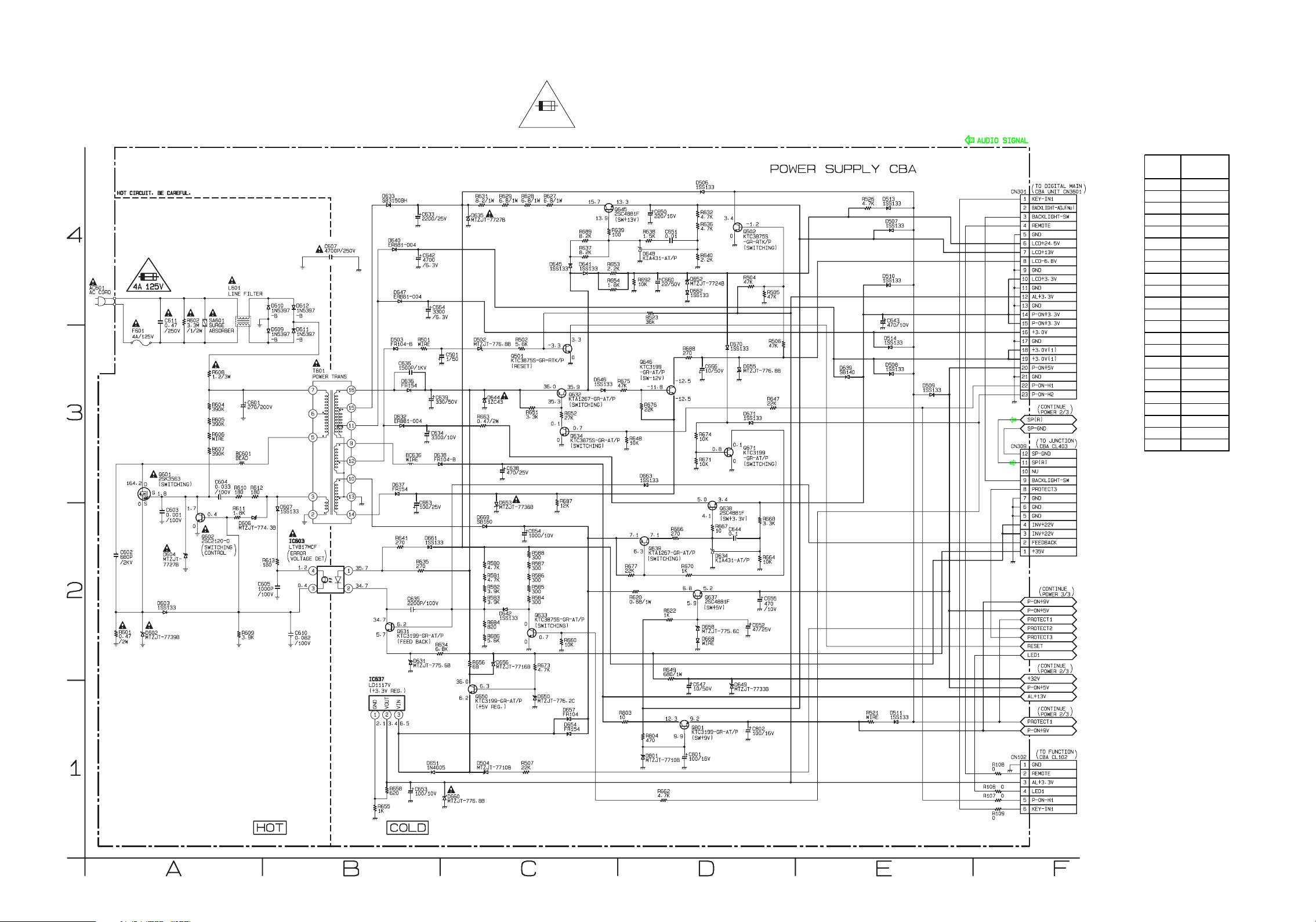
Power Supply 1/3 Schematic Diagram
CN301
13.4
20
33.3
43.4
50
6 24.9
7 13.3
8-7.0
90
10 3.4
11 0
12 3.4
13 0
14 3.4
15 3.4
16 3.5
17 0
18 3.5
19 3.5
20 5.2
21 0
22 3.3
23 3.2
VOLTAGE CHART
Pin No. Voltage
CAUTION !
Fixed voltage (or Auto voltage selectable) power supply circuit is used in this unit.
If Main Fuse (F601) is blown , check to see that all components in the power supply
circuit are not defective before you connect the AC plug to the AC power supply.
Otherwise it may cause some components in the power supply circuit to fail.
4A/125V
CAUTION ! :
For continued protection against risk of fire,
replace only with same type 4 A, 125V fuse.
ATTENTION : Utiliser un fusible de rechange de même type de 4A, 125V.
NOTE:
The voltage for parts in hot circuit is measured using
hot GND as a common terminal.
8-3
A8AN4SCP1
Page 31
Power Supply 2/3 Schematic Diagram
CN303
15.2
20
32.6
42.6
50
60
70
80
91.9
10 0
11 1.6
12 --13 0
14 0
15 5.0
16 4.9
17 0
18 0
19 0
20 ~
21 0
22 ~
23 0
VOLTAGE CHART
Pin No. Voltage
8-4
A8AN4SCP2
Page 32

Power Supply 3/3 Schematic Diagram
CN302
13.4
20
33.4
43.4
50
61.7
71.6
80
91.7
10 1.7
11 0
12 1.0
13 0
14 0
15 0
16 0
17 0
18 0
19 0
20 0
21 0
22 0
23 0
VOLTAGE CHART
Pin No. Voltage
8-5
A8AN4SCP3
Page 33

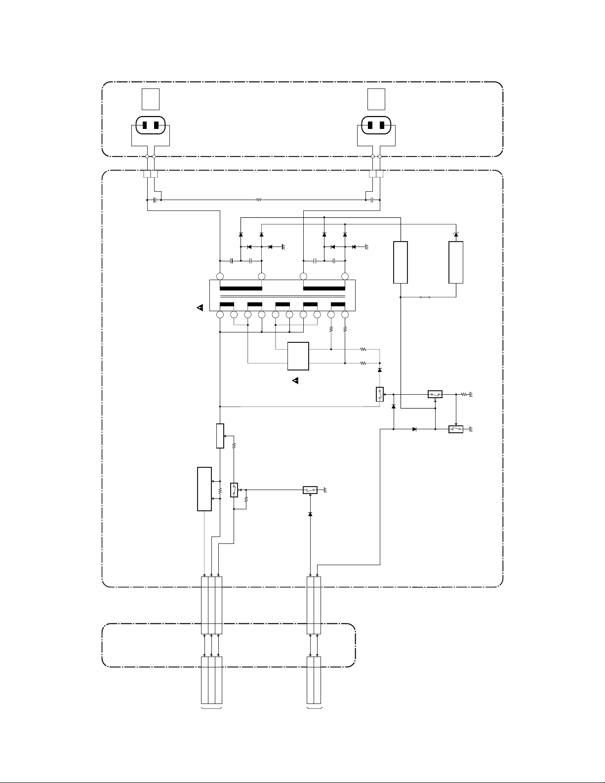
Inverter & Junction Schematic Diagram
8-6
A8AN4SCINV
Page 34

Function Schematic Diagram
8-7
A8AN4SCF
Page 35

IR Sensor Schematic Diagram
8-8
A8AN4SCIR
Page 36

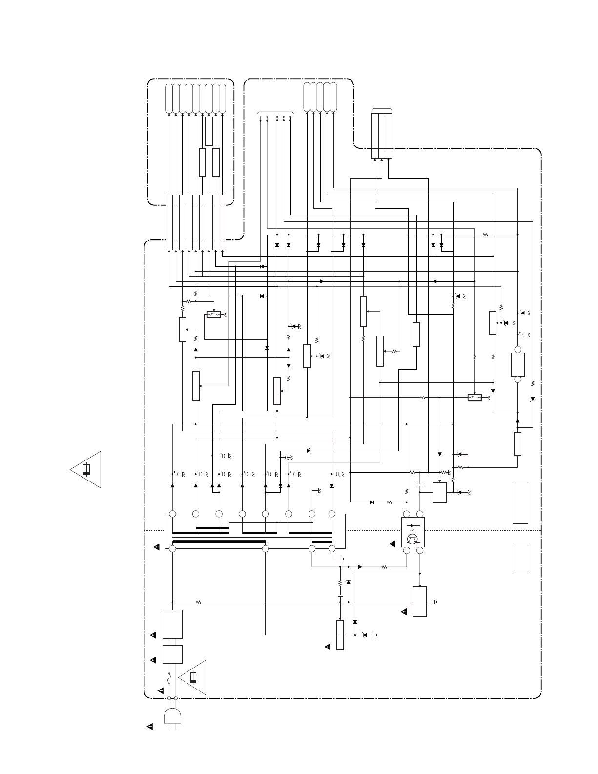
Digital Main 1/4 Schematic Diagram
1 NOTE:
The order of pins shown in this diagram is different from that of actual IC3301.
IC3301 is divided into four and shown as IC3301 (1/4) ~ IC3301 (4/4) in this Digital Main Schematic Diagram Section.
8-9
A8AN4SCD1
Page 37

Digital Main 2/4 Schematic Diagram
1 NOTE:
The order of pins shown in this diagram is different from that of actual IC3301.
IC3301 is divided into four and shown as IC3301 (1/4) ~ IC3301 (4/4) in this Digital Main Schematic Diagram Section.
8-10
A8AN4SCD2
Page 38

Digital Main 3/4 Schematic Diagram
1 NOTE:
The order of pins shown in this diagram is different from that of actual IC3301.
IC3301 is divided into four and shown as IC3301 (1/4) ~ IC3301 (4/4) in this Digital Main Schematic Diagram Section.
8-11
A8AN4SCD3
Page 39

Digital Main 4/4 Schematic Diagram
1 NOTE:
The order of pins shown in this diagram is different from that of actual IC3301.
IC3301 is divided into four and shown as IC3301 (1/4) ~ IC3301 (4/4) in this Digital Main Schematic Diagram Section.
8-12
A8AN4SCD4
Page 40

Power Supply CBA Top View
Because a hot chassis ground is present in the power
supply circuit, an isolation transformer must be used.
Also, in order to have the ability to increase the input
slowly,when troubleshooting this type power supply
circuit, a variable isolation transformer is required.
NOTE:
The voltage for parts in hot circuit is measured using
hot GND as a common terminal.
CAUTION !
Fixed voltage (or Auto voltage selectable) power supply circuit is used in this unit.
If Main Fuse (F601) is blown , check to see that all components in the power supply
circuit are not defective before you connect the AC plug to the AC power supply.
Otherwise it may cause some components in the power supply circuit to fail.
4A/125V
CAUTION ! :
ATTENTION : Utiliser un fusible de rechange de même type de 4A, 125V.
For continued protection against risk of fire,
replace only with same type 4 A, 125V fuse.
8-13
BA8AN0F01012-1
Page 41

Power Supply CBA Bottom View
Because a hot chassis ground is present in the power
supply circuit, an isolation transformer must be used.
Also, in order to have the ability to increase the input
slowly,when troubleshooting this type power supply
circuit, a variable isolation transformer is required.
NOTE:
The voltage for parts in hot circuit is measured using
hot GND as a common terminal.
CAUTION !
Fixed voltage (or Auto voltage selectable) power supply circuit is used in this unit.
If Main Fuse (F601) is blown , check to see that all components in the power supply
circuit are not defective before you connect the AC plug to the AC power supply.
Otherwise it may cause some components in the power supply circuit to fail.
4A/125V
CAUTION ! :
ATTENTION : Utiliser un fusible de rechange de même type de 4A, 125V.
For continued protection against risk of fire,
replace only with same type 4 A, 125V fuse.
WF7
PIN 3 OF
CN303
WF1
PIN 23 OF
CN302
WF3
PIN 21 OF
CN302
WF2
PIN 19 OF
CN302
WF6
PIN 17 OF
CN302
WF5
PIN 16 OF
CN302
WF4
PIN 14 OF
CN302
8-14
BA8AN0F01012-1
Page 42
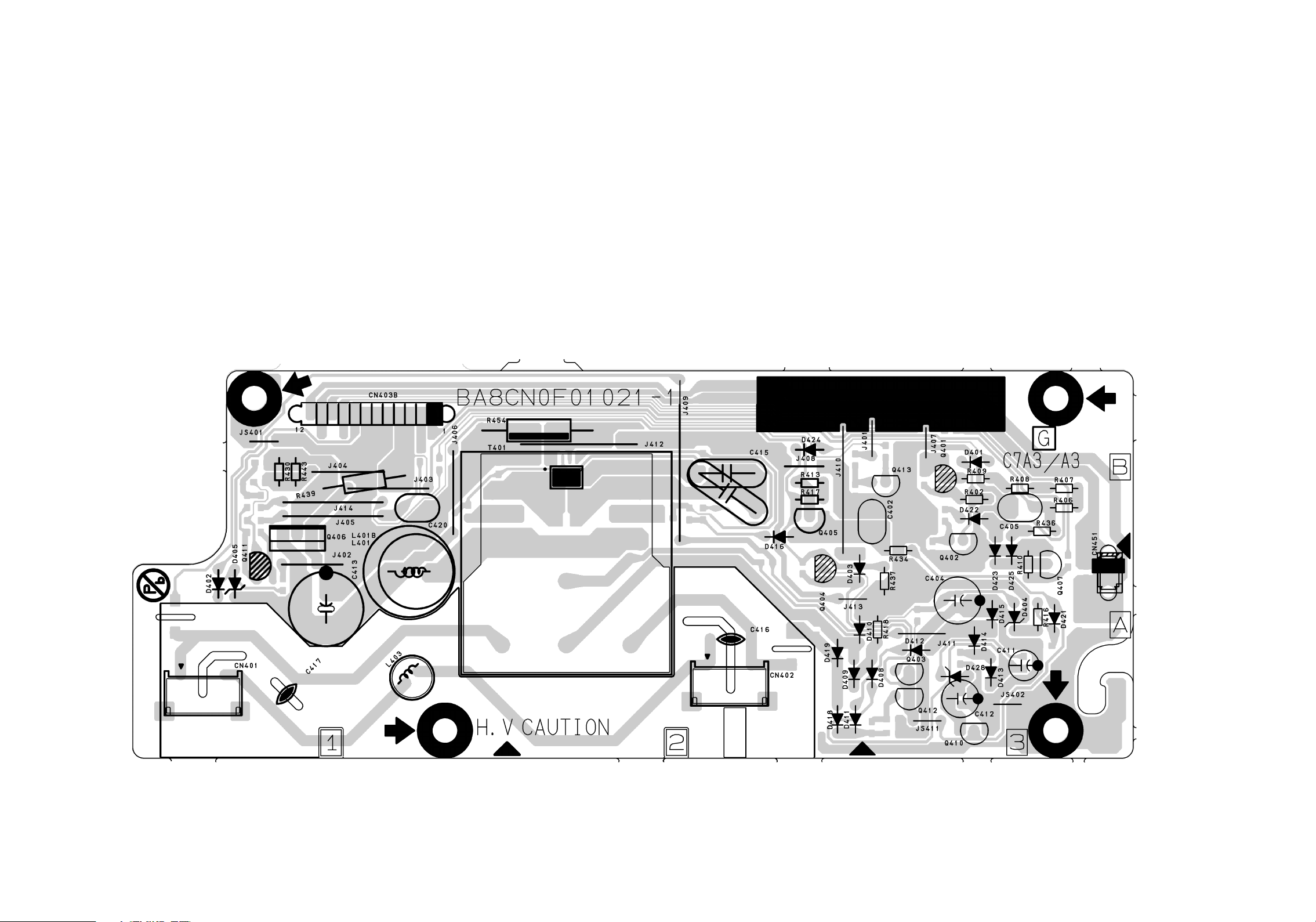
Inverter CBA Top View
8-15
BA8CN0F01021
Page 43

Inverter CBA Bottom View
8-16
BA8CN0F01021
Page 44

Function CBA Top View
Function CBA Bottom View
8-17
BA8AN0F01012-2
Page 45

IR Sensor CBA Top View
Junction CBA Top View Junction CBA Bottom View
BA8CN0F01021
IR Sensor CBA Bottom View
BA8AN0F01012-3
8-18
Page 46
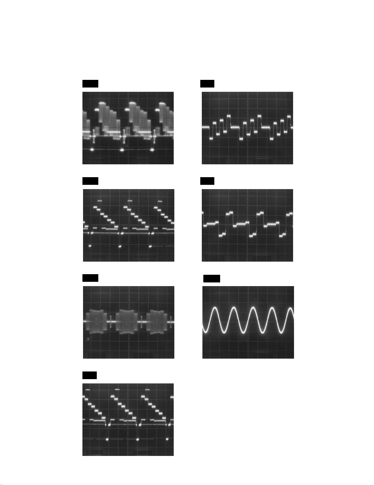
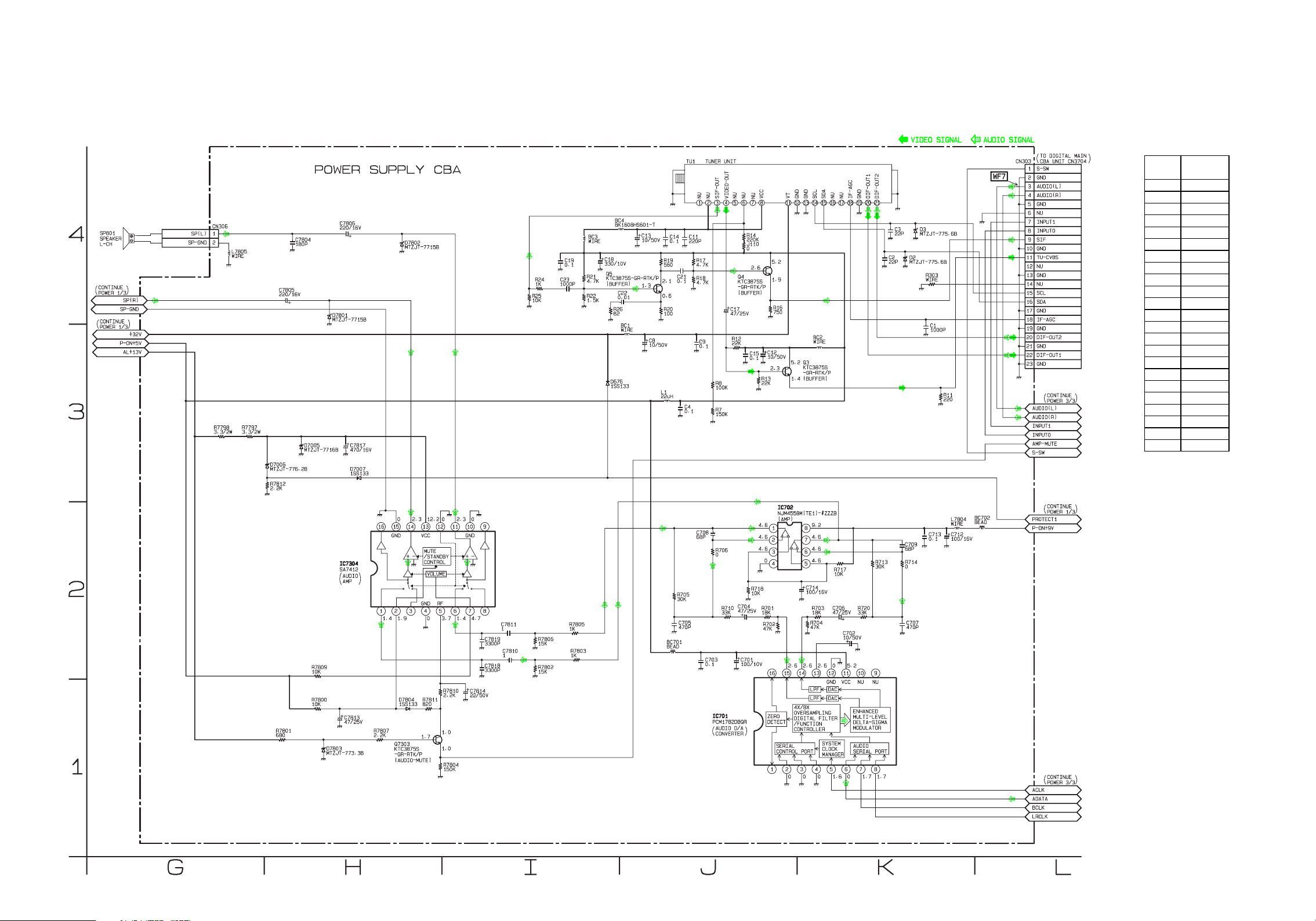
WAVEFORMS
WF1 ~ WF7 = Waveforms to be observed at
Waveform check points.
(Shown in Schematic Diagram.)
Input: NTSC Color Bar Signal (with 1kHz Audio Signal)
WF1
WF2
Pin 23 of CN302
VIDEO 0.2V 20µs
Pin 19 of CN302
S-VIDEO-Y 0.2V
20µs
WF5
WF6
Pin 16 of CN302
COMP-Pb 0.2V 20µs
Pin 17 of CN302
COMP-Pr 0.2V 20µs
WF3
WF4
Pin 21 of CN302
S-VIDEO-C 0.2V
Pin 14 of CN302
COMP-Y 0.2V 20µs
20µs
WF7
Pin 3 of CN303
AUDIO 1V 0.5ms
A8AN4WF9-1
Page 47
WIRING DIAGRAM
DIGITAL MAIN CBA UNIT
STH-F54GND53FRSB2(+)52FRSB2(-)51FRSB1(+)50FRSB1(-)49FRSB0(+)48FRSB0(-)47FRSG2(+)46FRSG2(-)45FRSG1(+)44FRSG1(-)
55
CN4502
CN4501
55
54
53
52
51
48
GND
GND
VEEG
BRSB2(-)49BRSB1(-)
BRSB2(+)50BRSB1(+)
BRSB0(+)
BACK
LIGHT
2
1
CN401
D-SUB
CONNECTOR
HDMI-
CONNECTOR-2
47
46
BRSB0(-)
BRSG2(+)
BACK
1
CN402
45
BRSG2(-)
LIGHT
2
43 FRSG0(+)
42 FRSG0(-)
44
43BRSG1(-)
42BRSG0(+)
BRSG1(+)
41 GND
40 GMA14
41BRSG0(-)
40GND
39 GMA13
38 GMA12
39GMA14
38GMA13
37 GMA11
36 GMA10
37GMA12
36GMA11
35 GMA9
34 GMA8
35GMA10
34GMA9
SP801
SPEAKER
33 VDDA
33GMA8
L-CH
32 VDDA
32VDDA
CN451
31 GMA7
30 GMA6
31VDDA
30GMA7
SP(R)
1
SP802
SPEAKER
29 GMA5
29GMA6
SP-GND
2
R-CH
28 GMA4
28GMA5
27 GMA3
27GMA4
26 GMA2
26GMA3
25 GMA1
25GMA2
24 GND
23 FRSCLK(+)
24GMA1
23GND
22 FRSCLK(-)
21 GND
22BRSCLK(+)
21BRSCLK(-)
CL403B
1
+35V
1
CL403A
CL403
1
20 TP1
20GND
2
FEEDBACK
2
2
19 POL
19TP1
3
4
INV+22V
3 INV+22V
4
3
4
18 FRSR2(+)
17 FRSR2(-)
18POL
17BRSR2(+)
5
GND
GND
5
5
16 FRSR1(+)
15 FRSR1(-)
16BRSR2(-)
15BRSR1(+)
7
8
PROTECT3
7 GND66
8
7
8
14 FRSR0(+)
13 FRSR0(-)
12 GND
14BRSR1(-)
13BRSR0(+)
12BRSR0(-)
9
10
BACKLIGHT-SW
9
10 NU
9
10
11
SP(R)
11
11
11 VDDD
10 VDDD
11STH-S
10GND
12
SP-GND
12
12
9 VCOM
9VDDD
8 VEEG
8VDDD
INVERTER CBA
JUNCTION CBA
7 STV
7VCOM
6 CPV
6GND
5 OE1
5STV
4 XAO
4GND
3 GND
3GND
CL102
2 VDDG
1 GND
2GND
1GND
CL101B
P-ON-H1
CL101A
6
4
4 LED155
4
3
2
AL+3.3V
REMOTE
3
2
3
2
1
GND
1
1
LCD MODULE ASSEMBLY
IR SENSOR CBAFUNCTION CBA
HDMI-
CONNECTOR-1
CN301CN3601
KEY-IN1
23
4
2
BACKLIGHT-ADJ(NU)
BACKLIGHT-SW
REMOTE
21
22
20
COMPONENT
-Y-IN1
COMPONENT
6
513
GND
LCD+24.5V
18
19
-Pb-IN1
8
9
7
LCD+13V
LCD-6.8V
GND
LCD+3.3V
15
17
16
14
COMPONENT-
COMPONENT
-Pr-IN1
13
11
GND
AL+3.3V
GND
12
11
13
AUDIO(L)-IN1
COMPONENT-
AUDIO(R)-IN1
CN306
15
16
141012
P-ON+3.3V
P-ON+3.3V
+3.0V
9
8
10
VIDEO-IN1
1
2
SP(L)
SP-GND
172220
18
GND
+3.0V(1)
+3.0V(1)
513
6
7
AUDIO(L)
-IN1
P-ON+5V
GND
4
AUDIO(R)
-IN1
AC CORD
AC601
231921
P-ON-H1
P-ON-H2
2
CN303CN3704
CN3701CN302
S-VIDEO
-IN1
2
S-SW
GND
23
22
23
22
PROTECT1
PROTECT2
2
PC-AUDIO
-IN
CN309
4
AUDIO(L)
AUDIO(R)
21
20
21
20
PROTECT3
RESET
4
HDMI-
+35V
FEEDBACK
INV+22V
1
3 INV+22V
2
4
6
7
513
GNDNUINPUT1
17
18
19
17
18
19
GND
SPDIF
ACLK
6
7
513
AUDIO(L)-IN2
HDMI-
AUDIO(R)-IN2
GND
5
8
9
INPUT0
SIF
15
16
15
16
ADATA
BCLK
8
9
GND
PROTECT3
7 GND66
8
11
GND
TU-CVBSNUGNDNUSCL
12
14
13
12
14
13
LRCLK
GND
AMP-MUTE
11
DIGITAL
AUDIO-OUT
(COAXIAL)
BACKLIGHT-SW
9
13
11
11
LED1
13
SP(R)
10 NU
11
141012
10
10
COMP-Y
141012
SP-GND
12
15
9
9
GND
15
172220
16
SDA
GND
8
7
8
7
COMP-Pb
COMP-Pr
172220
16
18
IF-AGC
GND
513
6
513
6
GND
S-VIDEO-Y
18
DIF-OUT2
GND
DIF-OUT1
2
4
2
4
GND
S-VIDEO-C
GND
CN102
231921
GND
VIDEO
231921
KEY-IN1
6
P-ON-H1
4 LED155
AL+3.3V
REMOTE
3
2
GND
1
POWER SUPPLY CBA
TU1 TUNER UNIT
A8AN4WI10-1
Page 48

Cabinet
EXPLODED VIEWS
A1
A26
A3
A11
A7
A5
SP802
SP801
L30
Function CBA
IR Sensor CBA
L30
See Electrical Parts List
for parts with this mark.
CL4501
L10
Inverter CBA
CL4502
B17
L10
LCD1
L10
L10
Junction CBA
L10
B20
L9
L28
L10
L10
B36
Power Supply CBA
B38
L10
B21
L9
Digital Main CBA Unit
B8
B36
L10
L10
B3
L30
B3
L3
L11
L30
L3
L10
B3
A24
L5
B14
L10
L11
L17
A4
A10
L3
L11
L3
A6
L3
S5
AC601
A9
A12
11-1 A8AN4CEX
Page 49

Packing
e
Some Ref. Numbers are
not in sequence.
X4
Packing Tape
S2
S16
Packing Tape
X3
X2X14
Ta p
Packing Tape
FRONT
S4
S3
S5
Packing Tape
FRONT
S3
X1
S1
11-2 A8AN4PEX
Page 50

MECHANICAL PARTS LIST
PRODUCT SAFETY NOTE: Products marked with a
# have special characteristics important to safety.
Before replacing any of these components, read
carefully the product safety notice in this service
manual. Don't degrade the safety of the product
through improper servicing.
NOTE: Parts that are not assigned part numbers
(---------) are not available.
Ref. No. Description Part No.
A1 FRONT CABINET A8AN0UH 1EM122613
A3 CONTROL PLATE A8AN0UH 1EM324757
A4 REAR CABINET A8AN0UH 1EM022545
A5 DECORATION PLATE A8CN0FP 1EM222223
A6# RATING LABEL A8AN4UH ---------A7 FUNCTION KNOB A8CN0FP 1EM222143
A9 STAND COVER A8CN0FP 1EM022467
A10 CONNECTOR CAP A8AN0UH 1EM426557
A11 SENSOR LED LENS A8CN0FP 1EM323959
A12 STAND RUBBER FOOT A8AN0UH 1EM426377
A24 STAND NECK A8CN0FP 1EM122513
A26 LOGO LABEL A8AF1UH ---------B3 WALL MOUNT BRACKET A84N0UH 1EM323797
B8 SHIELD BOX A8AN0UH 1EM222203
B14 FIX STAND HOLDER A8AN0UH 1EM323938
B17 SEPARATION SHEET A8AN0UH 1EM324520
B36 GASKET A8AF0UH 1EM425861
B38 TUNER HOLDER A8AN0UH 1EM324097
CL4501 WIRE ASSEMBLY 55PIN WX1A8CN0-007 WX1A8CN0-007
CL4502 WIRE ASSEMBLY 55PIN WX1A8CN0-007 WX1A8CN0-007
L3 SCREW P-TIGHT 3X10 BIND HEAD+ GBHP3100
L5 SCREW P-TIGHT M4X18 BIND HEAD+ GBHP4180
L10 SCREW S-TIGHT M3X6 BIND HEAD+ GBJS3060
L11 SCREW S-TIGHT M3X8 BIND HEAD+ GBHS3080
L17 DOUBLE SEMS SCREW M4X9 + BLACK
L28 HEX SCREW #4-40 7MM 1EM422042
L30 SCREW P-TIGHT M3X10 BIND HEAD+ GBJP3100
LCD1 LCD MODULE 19INCH WIDE CMO 19INCH
SP801 SPEAKER MAGNETIC S0306N01 DSD0806XQ001
SP802 SPEAKER MAGNETIC S0306N01 DSD0806XQ001
L0130UA
WXGA
PACKING
S1 CARTON A8AN0UH 1EM426157
S2 STYROFOAM TOP A8AN0UH 1EM022565
S3 STYROFOAM BTM A8AN0UH 1EM022566
S4 SET BAG A81N0UH 1EM323958
S5 SERIAL NO. LABEL L9750UA ---------S16 STAND BAG A81N0UH 1EM425888
ACCESSORIES
X1 BAG POLYETHYLENE 235X365XT0.03 0EM408420A
X2# OWNERS MANUAL A8AN0UH 1EMN23119
X3 REMOTE CONTROL NF015UD 170/
X4 DRY BATTERY(SUNRISE) R6SSE/2S XB0M451MS002
X14 FCC ADDENDUM SHEET E9H10UD 1VMN25693
ECNLC501/NF015UD
0EM408146A
UG190XF
NF015UD
20080418 12-1 A8AN4CA
Page 51

ELECTRICAL PARTS LIST
PRODUCT SAFETY NOTE: Products marked with a
# have special characteristics important to safety.
Before replacing any of these components, read
carefully the product safety notice in this service
manual. Don't degrade the safety of the product
through improper servicing.
NOTES:
1. Parts that are not assigned part numbers (---------)
are not available.
2. Tolerance of Capacitors and Resistors are noted
with the following symbols.
C.....±0.25% D.....±0.5% F.....±1%
G.....±2% J......±5% K.....±10%
M.....±20% N.....±30% Z.....+80/-20%
DIGITAL MAIN CBA UNIT
Ref. No. Description Part No.
DIGITAL MAIN CBA UNIT 1ESA17487
MPS CBA
Ref. No. Description Part No.
MPS CBA
Consists of the following
POWER SUPPLY CBA(MPS-1)
FUNCTION CBA(MPS-2)
IR SENSOR CBA(MPS-3)
POWER SUPPLY CBA
Ref. No. Description Part No.
POWER SUPPLY CBA(MPS-1)
Consists of the following:
CAPACITORS
C1 CHIP CERAMIC CAP.(1608) CH J 1000pF/50V CHD1JJ3CH102
C2 CHIP CERAMIC CAP.(1608) CH J 22pF/50V CHD1JJ3CH220
C3 CHIP CERAMIC CAP.(1608) CH J 22pF/50V CHD1JJ3CH220
C4 CHIP CERAMIC CAP.(1608) F Z 0.1µF/25V CHD1EZ30F104
C8 ELECTROLYTIC CAP. 10µF/50V M CE1JMASDL100
C9 CHIP CERAMIC CAP.(1608) F Z 0.1µF/50V CHD1JZ30F104
C11 CHIP CERAMIC CAP. CH J 220pF/50V CHD1JJ3CH221
C12 ELECTROLYTIC CAP. 10µF/50V M CE1JMASDL100
C13 ELECTROLYTIC CAP. 10µF/50V M H7 CE1JMAVSL100
C14 CHIP CERAMIC CAP.(1608) F Z 0.1µF/25V CHD1EZ30F104
C15 CHIP CERAMIC CAP.(1608) F Z 0.1µF/25V CHD1EZ30F104
C17 ELECTROLYTIC CAP. 47µF/25V M CE1EMASDL470
C18 ELECTROLYTIC CAP. 330µF/10V M CE1AMASDL331
C19 CHIP CERAMIC CAP.(1608) F Z 0.1µF/25V CHD1EZ30F104
C21 CHIP CERAMIC CAP.(1608) F Z 0.1µF/25V CHD1EZ30F104
C22 CHIP CERAMIC CAP.(1608) B K 0.01µF/50V CHD1JK30B103
C23 CHIP CERAMIC CAP.(1608) CH J 1000pF/50V CHD1JJ3CH102
C501 ELECTROLYTIC CAP. 1µF/50V M CE1JMASDL1R0
C601 CAP ELE LT 270µF/200V/M/85 CA2D271V8005
C602 CERAMIC CAP. R K 680pF/2KV(HR) CCD3DKA0R681
C603 POLYESTER FILM CAP. (PB FREE) 0.001µF/
C604 POLYESTER FILM CAP. (PB FREE) 0.033µF/
100V J
100V J
1ESA17485
----------
----------
----------
----------
CA2A102DT018
CA2A333DT018
Ref. No. Description Part No.
C605 POLYESTER FILM CAP. (PB FREE) 0.001µF/
C607# CAP CERAMIC 4700pF/250V/M/KX CA2E472MR101
C610 POLYESTER FILM CAP. (PB FREE) 0.082µF/
C611# METALIZED FILM CAP. 0.47µF/250V CT2E474MS037
C633 ELECTROLYTIC CAP. 2200µF/25V M CE1EMZNDL222
C634 ELECTROLYTIC CAP 3300µF/10V CE1AMZNDL332
C635 POLYESTER FILM CAP. (PB FREE) 0.0022µF/
C636 CERAMIC CAP. B K 1500pF/1KV CCD3AKP0B152
C638 ELECTROLYTIC CAP. 470µF/25V M CE1EMZADL471
C639 ELECTROLYTIC CAP 330µF/50V M CE1JMZADL331
C642 CAP ELE STD-85 4700µF 6.3V SL CE0KMZNDL472
C643 ELECTROLYTIC CAP. 470µF/10V M CE1AMASDL471
C644 CHIP CERAMIC CAP.(1608) B K 0.1µF/50V CHD1JK30B104
C647 ELECTROLYTIC CAP. 10µF/50V M CE1JMASDL100
C650 ELECTROLYTIC CAP. 220µF/16V M CE1CMASDL221
C651 CHIP CERAMIC CAP.(1608) B K 0.01µF/50V CHD1JK30B103
C652 ELECTROLYTIC CAP. 47µF/25V M CE1EMASDL470
C653 ELECTROLYTIC CAP. 100µF/10V M CE1AMASDL101
C654 ELECTROLYTIC CAP. 1000µF/10V M CE1AMASDL102
C655 ELECTROLYTIC CAP. 470µF/10V M CE1AMASDL471
C660 ELECTROLYTIC CAP. 22µF/50V M(105C) CE1JMASTH220
C663 ELECTROLYTIC CAP. 100µF/25V M CE1EMASDL101
C664 ELECTROLYTIC CAP 3300µF/6.3V M CE0KMZNDL332
C666 ELECTROLYTIC CAP. 10µF/50V M CE1JMASDL100
C701 ELECTROLYTIC CAP. 100µF/10V M CE1AMASDL101
C702 ELECTROLYTIC CAP. 10µF/50V M CE1JMASDL100
C703 CHIP CERAMIC CAP.(1608) F Z 0.1µF/25V CHD1EZ30F104
C704 ELECTROLYTIC CAP. 47µF/25V M CE1EMASDL470
C705 CHIP CERAMIC CAP. B K 470pF/50V CHD1JK30B471
C706 ELECTROLYTIC CAP. 47µF/25V M CE1EMASDL470
C707 CHIP CERAMIC CAP. B K 470pF/50V CHD1JK30B471
C708 CHIP CERAMIC CAP.(1608) CH J 68pF/50V CHD1JJ3CH680
C709 CHIP CERAMIC CAP.(1608) CH J 68pF/50V CHD1JJ3CH680
C712 ELECTROLYTIC CAP. 100µF/16V M CE1CMASDL101
C713 CHIP CERAMIC CAP.(1608) F Z 0.1µF/25V CHD1EZ30F104
C714 ELECTROLYTIC CAP. 100µF/16V M CE1CMASDL101
C801 ELECTROLYTIC CAP. 100µF/16V M CE1CMASDL101
C802 ELECTROLYTIC CAP. 100µF/16V M CE1CMASDL101
C7201 CHIP CERAMIC CAP. F Z 1µF/10V CHD1AZ30F105
C7202 PCB JUMPER D0.6-P5.0 JW5.0T
C7204 CHIP CERAMIC CAP.(1608) B K 0.01µF/50V CHD1JK30B103
C7301 CHIP CERAMIC CAP.(1608) CH J 100pF/50V CHD1JJ3CH101
C7302 CHIP CERAMIC CAP.(1608) CH J 100pF/50V CHD1JJ3CH101
C7303 CHIP CERAMIC CAP.(1608) F Z 0.1µF/25V CHD1EZ30F104
C7304 ELECTROLYTIC CAP. 100µF/16V M CE1CMASDL101
C7307 ELECTROLYTIC CAP. 4.7µF/50V M CE1JMASDL4R7
C7308 ELECTROLYTIC CAP. 4.7µF/50V M CE1JMASDL4R7
C7401 ELECTROLYTIC CAP. 4.7µF/50V M H7 CE1JMAVSL4R7
C7402 ELECTROLYTIC CAP. 4.7µF/50V M H7 CE1JMAVSL4R7
C7515 ELECTROLYTIC CAP. 4.7µF/50V M H7 CE1JMAVSL4R7
C7516 ELECTROLYTIC CAP. 4.7µF/50V M H7 CE1JMAVSL4R7
C7602 ELECTROLYTIC CAP. 4.7µF/50V M H7 CE1JMAVSL4R7
C7605 ELECTROLYTIC CAP. 4.7µF/50V M H7 CE1JMAVSL4R7
C7615 ELECTROLYTIC CAP. 4.7µF/50V M CE1JMASDL4R7
C7618 ELECTROLYTIC CAP. 4.7µF/50V M H7 CE1JMAVSL4R7
C7701 CHIP CERAMIC CAP.(1608) CH J 100pF/50V CHD1JJ3CH101
C7702 CHIP CERAMIC CAP. F Z 0.47µF/16V CHD1CZ30F474
C7709 CHIP CERAMIC CAP.(1608) CH J 100pF/50V CHD1JJ3CH101
100V J
100V J
100V J
CA2A102DT018
CA2A823DT018
CA2A222DT018
20080418 13-1 A8AN4EL
Page 52

Ref. No. Description Part No.
C7710 CHIP CERAMIC CAP. F Z 0.47µF/16V CHD1CZ30F474
C7714 CHIP CERAMIC CAP.(1608) CH J 100pF/50V CHD1JJ3CH101
C7715 CHIP CERAMIC CAP.(1608) B K 0.047µF/50V CHD1JK30B473
C7729 CHIP CERAMIC CAP. CH J 39pF/50V CHD1JJ3CH390
C7730 CHIP RES.(1608) 1/10W 0 Ω RRXAZR5Z0000
C7733 CHIP CERAMIC CAP. CH J 39pF/50V CHD1JJ3CH390
C7734 CHIP RES.(1608) 1/10W 0 Ω RRXAZR5Z0000
C7738 CHIP CERAMIC CAP. CH J 39pF/50V CHD1JJ3CH390
C7739 CHIP RES.(1608) 1/10W 0 Ω RRXAZR5Z0000
C7804 CHIP CERAMIC CAP. CH J 180pF/50V CHD1JJ3CH181
C7805 ELECTROLYTIC CAP. 220µF/16V M H7 CE1CMASSL221
C7806 ELECTROLYTIC CAP. 220µF/16V M H7 CE1CMASSL221
C7810 CHIP CERAMIC CAP. F Z 1µF/10V CHD1AZ30F105
C7811 CHIP CERAMIC CAP. F Z 1µF/10V CHD1AZ30F105
C7813 ELECTROLYTIC CAP. 47µF/25V M CE1EMASDL470
C7814 ELECTROLYTIC CAP. 22µF/50V M CE1JMASDL220
C7817 ELECTROLYTIC CAP. 470µF/16V M CE1CMASDL471
C7818 CHIP CERAMIC CAP.(1608) B K 3300pF/50V CHD1JK30B332
C7819 CHIP CERAMIC CAP.(1608) B K 3300pF/50V CHD1JK30B332
CONNECTORS
CN301 TWG CONNECTOR 23P TWG-P23P-A1 J3TWA23TG001
CN302 TWG CONNECTOR 23P TWG-P23P-A1 J3TWA23TG001
CN303 TWG CONNECTOR 23P TWG-P23P-A1 J3TWA23TG001
CN306 WIRE ASSEMBLY SPEAKER 2PIN 2PIN /95MM WX1A8AN0-003
CN309 242 SERIES CONNECTOR 224202112W1 J322C12TG001
DIODES
D2 ZENER DIODE MTZJT-775.6B QDTB0MTZJ5R6
D3 ZENER DIODE MTZJT-775.6B QDTB0MTZJ5R6
D502 ZENER DIODE MTZJT-776.8B QDTB0MTZJ6R8
D503 DIODE FR104-B NDLZ000FR104
D504 ZENER DIODE MTZJT-7710B QDTB00MTZJ10
D506 SWITCHING DIODE 1SS133(T-77) QDTZ001SS133
D507 SWITCHING DIODE 1SS133(T-77) QDTZ001SS133
D508 SWITCHING DIODE 1SS133(T-77) QDTZ001SS133
D509 SWITCHING DIODE 1SS133(T-77) QDTZ001SS133
D510 SWITCHING DIODE 1SS133(T-77) QDTZ001SS133
D511 SWITCHING DIODE 1SS133(T-77) QDTZ001SS133
D513 SWITCHING DIODE 1SS133(T-77) QDTZ001SS133
D514 SWITCHING DIODE 1SS133(T-77) QDTZ001SS133
D602# ZENER DIODE MTZJT-7739B QDTB00MTZJ39
D603 SWITCHING DIODE 1SS133(T-77) QDTZ001SS133
D604# ZENER DIODE MTZJT-7727B QDTB00MTZJ27
D606 ZENER DIODE MTZJT-774.3B QDTB0MTZJ4R3
D607 SWITCHING DIODE 1SS133(T-77) QDTZ001SS133
D609 DIODE 1N5397-B NDLZ001N5397
D610 DIODE 1N5397-B NDLZ001N5397
D611 DIODE 1N5397-B NDLZ001N5397
D612 DIODE 1N5397-B NDLZ001N5397
D631 ZENER DIODE MTZJT-775.6B QDTB0MTZJ5R6
D632 SCHOTTKY BARRIER DIODE ERB81-004 AERB81004***
D633 DIODE SCHOTTKY SB3150BH NDWZ00SB3150
D634 IC SHUNT REGULATOR KIA431-AT/P NSZBA0TJY036
D635# ZENER DIODE MTZJT-7727B QDTB00MTZJ27
D636 DIODE FR154 NDLZ000FR154
D637 DIODE FR154 NDLZ000FR154
D638 DIODE FR104-B NDLZ000FR104
D639 SCHOTTKY BARRIER DIODE SB140 NDQZ000SB140
D640 SCHOTTKY BARRIER DIODE ERB81-004 AERB81004***
D641 SWITCHING DIODE 1SS133(T-77) QDTZ001SS133
D642 SWITCHING DIODE 1SS133(T-77) QDTZ001SS133
D644# DIODE 1ZC43(Q) QDLZ001ZC43Q
D645 SWITCHING DIODE 1SS133(T-77) QDTZ001SS133
Ref. No. Description Part No.
D646 SWITCHING DIODE 1SS133(T-77) QDTZ001SS133
D647 SCHOTTKY BARRIER DIODE ERB81-004 AERB81004***
D648 IC SHUNT REGULATOR KIA431-AT/P NSZBA0TJY036
D649 ZENER DIODE MTZJT-7733B QDTB00MTZJ33
D650 ZENER DIODE MTZJT-776.2C QDTC0MTZJ6R2
D651 RECTIFIER DIODE 1N4005 NDQZ001N4005
D652 ZENER DIODE MTZJT-7724B QDTB00MTZJ24
D653# ZENER DIODE MTZJT-7736B QDTB00MTZJ36
D654 DIODE FR154 NDLZ000FR154
D655 ZENER DIODE MTZJT-776.8B QDTB0MTZJ6R8
D656 ZENER DIODE MTZJT-7716B QDTB00MTZJ16
D657 DIODE FR154 NDLZ000FR154
D658 ZENER DIODE MTZJT-775.6C QDTC0MTZJ5R6
D660# ZENER DIODE MTZJT-776.8B QDTB0MTZJ6R8
D661 SWITCHING DIODE 1SS133(T-77) QDTZ001SS133
D662 SWITCHING DIODE 1SS133(T-77) QDTZ001SS133
D663 SWITCHING DIODE 1SS133(T-77) QDTZ001SS133
D668 PCB JUMPER D0.6-P5.0 JW5.0T
D669 SCHOTTKY BARRIER DIODE SB160 NDWZ000SB160
D670 SWITCHING DIODE 1SS133(T-77) QDTZ001SS133
D671 SWITCHING DIODE 1SS133(T-77) QDTZ001SS133
D676 SWITCHING DIODE 1SS133(T-77) QDTZ001SS133
D801 ZENER DIODE MTZJT-7710B QDTB00MTZJ10
D7005 ZENER DIODE MTZJT-7716B QDTB00MTZJ16
D7006 ZENER DIODE MTZJT-776.2B QDTB0MTZJ6R2
D7007 SWITCHING DIODE 1SS133(T-77) QDTZ001SS133
D7801 ZENER DIODE MTZJT-7715B QDTB00MTZJ15
D7802 ZENER DIODE MTZJT-7715B QDTB00MTZJ15
D7803 ZENER DIODE MTZJT-773.3B QDTB0MTZJ3R3
D7804 SWITCHING DIODE 1SS133(T-77) QDTZ001SS133
ICS
IC603# PHOTO COUPLER LTV817MCF NPECLTV817MF
IC637 IC LD1117V NSZBA0SSS046
IC701 IC(AUDIO D/A) PCM1782DBQR NSZBA0TTY192
IC702 IC OP AMP NJM4558M(TE1)-#ZZZB QSZBA0TJR089
IC7301 IC SWITCHING TC4052BF(ELNF) QSZBA0TTS162
IC7304 IC AUDIO SA7412 NSZBA0SQ0007
COILS
L1 CHOKE COIL 22µH-K LLBD00PKV021
L601# LINE FILTER 5.0MH 6Y075 LLBG00ZKT004
L7804 PCB JUMPER D0.6-P5.0 JW5.0T
L7805 PCB JUMPER D0.6-P5.0 JW5.0T
TRANSISTORS
Q3 CHIP TRANSISTOR KTC3875S-GR-RTK/P NQ14KTC3875S
Q4 CHIP TRANSISTOR KTC3875S-GR-RTK/P NQ14KTC3875S
Q5 CHIP TRANSISTOR KTC3875S-GR-RTK/P NQ14KTC3875S
Q501 CHIP TRANSISTOR KTC3875S-GR-RTK/P NQ14KTC3875S
Q502 CHIP TRANSISTOR KTC3875S-GR-RTK/P NQ14KTC3875S
Q601# FET MOS 2SK3563(Q) QFWZ2SK3563Q
Q602# TRANSISTOR 2SC2120-O(TE2 F T) QQS02SC2120F
Q631 TRANSISTOR KTC3199-GR-AT/P NQS4KTC3199P
Q632 TRANSISTOR KTA1267-GR-AT/P NQS1KTA1267P
Q633 CHIP TRANSISTOR KTC3875S-GR-RTK/P NQ14KTC3875S
Q634 CHIP TRANSISTOR KTC3875S-GR-RTK/P NQ14KTC3875S
Q637 NPN TRANSISTOR POWER 2SC4881F HFE
Q638 NPN TRANSISTOR POWER 2SC4881F HFE
Q639 TRANSISTOR KTA1267-GR-AT/P NQS1KTA1267P
Q645 NPN TRANSISTOR POWER 2SC4881F HFE
Q646 TRANSISTOR KTC3199-GR-AT/P NQS4KTC3199P
Q650 TRANSISTOR KTC3199-GR-AT/P NQS4KTC3199P
MAX320
MAX320
MAX320
QQWZ2SC4881F
QQWZ2SC4881F
QQWZ2SC4881F
20080418 13-2 A8AN4EL
Page 53

Ref. No. Description Part No.
Q671 TRANSISTOR KTC3199-GR-AT/P NQS4KTC3199P
Q801 TRANSISTOR KTC3199-GR-AT/P NQS4KTC3199P
Q7201 CHIP TRANSISTOR KTC3875S-GR-RTK/P NQ14KTC3875S
Q7301 CHIP TRANSISTOR KTC3875S-GR-RTK/P NQ14KTC3875S
Q7302 CHIP TRANSISTOR KTC3875S-GR-RTK/P NQ14KTC3875S
Q7303 CHIP TRANSISTOR KTC3875S-GR-RTK/P NQ14KTC3875S
RESISTORS
R7 CHIP RES. 1/10W J 150k Ω RRXAJR5Z0154
R8 CHIP RES. 1/10W J 100k Ω RRXAJR5Z0104
R11 CHIP RES. 1/10W J 220 Ω RRXAJR5Z0221
R12 CHIP RES. 1/10W J 22k Ω RRXAJR5Z0223
R13 CHIP RES. 1/10W J 22k Ω RRXAJR5Z0223
R14 CHIP RES. 1/10W J 220k Ω RRXAJR5Z0224
R16 CHIP RES. 1/10W J 750 Ω RRXAJR5Z0751
R17 CHIP RES. 1/10W J 4.7k Ω RRXAJR5Z0472
R18 CARBON RES. 1/4W J 4.7k Ω RCX4JATZ0472
R19 CHIP RES. 1/10W J 560 Ω RRXAJR5Z0561
R20 CHIP RES. 1/10W J 100 Ω RRXAJR5Z0101
R21 CHIP RES. 1/10W J 4.7k Ω RRXAJR5Z0472
R22 CHIP RES. 1/10W J 1.5k Ω RRXAJR5Z0152
R24 CARBON RES. 1/4W J 1k Ω RCX4JATZ0102
R25 CHIP RES. 1/10W J 10k Ω RRXAJR5Z0103
R26 CHIP RES. 1/10W J 82 Ω RRXAJR5Z0820
R106 CHIP RES.(1608) 1/10W 0 Ω RRXAZR5Z0000
R107 CHIP RES.(1608) 1/10W 0 Ω RRXAZR5Z0000
R108 CHIP RES.(1608) 1/10W 0 Ω RRXAZR5Z0000
R109 CHIP RES.(1608) 1/10W 0 Ω RRXAZR5Z0000
R303 PCB JUMPER D0.6-P5.0 JW5.0T
R501 PCB JUMPER D0.6-P5.0 JW5.0T
R502 CHIP RES. 1/10W F 5.6k Ω RRXAFR5H5601
R504 CHIP RES. 1/10W J 47k Ω RRXAJR5Z0473
R505 CHIP RES. 1/10W J 47k Ω RRXAJR5Z0473
R506 CHIP RES. 1/10W J 47k Ω RRXAJR5Z0473
R507 CHIP RES. 1/10W J 22k Ω RRXAJR5Z0223
R521 PCB JUMPER D0.6-P5.0 JW5.0T
R523 CHIP RES. 1/10W F 36k Ω RRXAFR5H3602
R526 CHIP RES. 1/10W J 4.7k Ω RRXAJR5Z0472
R580 CHIP RES. 1/10W F 4.7k Ω RRXAFR5H4701
R581 CHIP RES. 1/10W F 4.7k Ω RRXAFR5H4701
R582 CHIP RES. 1/10W F 3.9k Ω RRXAFR5H3901
R583 CHIP RES. 1/10W F 3.9k Ω RRXAFR5H3901
R584 CHIP RES. 1/10W F 300 Ω RRXAFR5H3000
R585 CHIP RES. 1/10W F 300 Ω RRXAFR5H3000
R586 CHIP RES. 1/10W F 300 Ω RRXAFR5H3000
R587 CHIP RES. 1/10W F 300 Ω RRXAFR5H3000
R588 CHIP RES. 1/10W F 300 Ω RRXAFR5H3000
R601# METAL OXIDE FILM RES. 2W J 0.47 Ω RN02R47DP004
R602# GLASS GLAZE RES. 1/2W J 3.3M Ω RXX2JZLZ0335
R604 CARBON RES. 1/4W J 390k Ω RCX4JATZ0394
R605 CARBON RES. 1/4W J 390k Ω RCX4JATZ0394
R606 PCB JUMPER D0.6-P5.0 JW5.0T
R607 CARBON RES. 1/4W J 390k Ω RCX4JATZ0394
R608# CEMENT RES. 3W K 1.2 Ω RW031R2PG007
R609 CARBON RES. 1/4W J 3.9k Ω RCX4JATZ0392
R610 CARBON RES. 1/4W J 180 Ω RCX4JATZ0181
R611 CARBON RES. 1/4W J 1.8k Ω RCX4JATZ0182
R612 CARBON RES. 1/4W J 180 Ω RCX4JATZ0181
R613 CARBON RES. 1/4W J 180 Ω RCX4JATZ0181
R620 METAL OXIDE FILM RES. 1W J 0.68 Ω RN01R68DP003
R622 CARBON RES. 1/4W J 1k Ω RCX4JATZ0102
R627 METAL OXIDE FILM RES. 1W J 6.8 Ω RN016R8DP003
R628 METAL OXIDE FILM RES. 1W J 6.8 Ω RN016R8DP003
Ref. No. Description Part No.
R629 METAL OXIDE FILM RES. 1W J 6.8 Ω RN016R8DP003
R631 METAL OXIDE FILM RES. 1W J 8.2 Ω RN018R2DP003
R632 CHIP RES. 1/10W F 4.7k Ω RRXAFR5H4701
R634 CARBON RES. 1/4W J 6.8k Ω RCX4JATZ0682
R635 CARBON RES. 1/4W J 270 Ω RCX4JATZ0271
R636 CHIP RES. 1/10W F 4.7k Ω RRXAFR5H4701
R637 CARBON RES. 1/4W J 8.2k Ω RCX4JATZ0822
R638 CHIP RES. 1/10W J 1.5k Ω RRXAJR5Z0152
R639 CARBON RES. 1/4W J 100 Ω RCX4JATZ0101
R640 CHIP RES. 1/10W F 2.2k Ω RRXAFR5H2201
R641 CARBON RES. 1/4W J 270 Ω RCX4JATZ0271
R647 CARBON RES. 1/4W J 22k Ω RCX4JATZ0223
R648 CHIP RES. 1/10W J 10k Ω RRXAJR5Z0103
R649 METAL OXIDE FILM RES. 1W J 680 Ω RN01681DP003
R651 CARBON RES. 1/4W J 3.3k Ω RCX4JATZ0332
R652 CARBON RES. 1/4W J 27k Ω RCX4JATZ0273
R653 CARBON RES. 1/4W J 2.2k Ω RCX4JATZ0222
R654 CARBON RES. 1/4W J 1.8k Ω RCX4JATZ0182
R655 CHIP RES. 1/10W F 1.0k Ω RRXAFR5H1001
R656 CARBON RES. 1/4W J 68 Ω RCX4JATZ0680
R658 CHIP RES. 1/10W F 620 Ω RRXAFR5H6200
R660 CHIP RES. 1/10W J 10k Ω RRXAJR5Z0103
R662 CHIP RES. 1/10W J 4.7k Ω RRXAJR5Z0472
R663 METAL OXIDE FILM RES. 2W J 0.47 Ω RN02R47DP004
R664 CHIP RES. 1/10W F 10k Ω RRXAFR5H1002
R666 CARBON RES. 1/4W J 270 Ω RCX4JATZ0271
R667 CARBON RES. 1/4W J 10 Ω RCX4JATZ0100
R668 CHIP RES. 1/10W F 3.3k Ω RRXAFR5H3301
R670 CARBON RES. 1/4W J 1k Ω RCX4JATZ0102
R671 CHIP RES. 1/10W J 10k Ω RRXAJR5Z0103
R673 CARBON RES. 1/4W J 4.7k Ω RCX4JATZ0472
R674 CHIP RES. 1/10W J 10k Ω RRXAJR5Z0103
R675 CARBON RES. 1/4W J 47k Ω RCX4JATZ0473
R676 CHIP RES. 1/10W J 22k Ω RRXAJR5Z0223
R677 CARBON RES. 1/4W J 22k Ω RCX4JATZ0223
R684 CHIP RES. 1/10W F 820 Ω RRXAFR5H8200
R686 CHIP RES. 1/10W F 5.6k Ω RRXAFR5H5601
R687 CARBON RES. 1/4W J 12k Ω RCX4JATZ0123
R688 CARBON RES. 1/4W J 270 Ω RCX4JATZ0271
R689 CARBON RES. 1/4W J 8.2k Ω RCX4JATZ0822
R692 CARBON RES. 1/4W J 10k Ω RCX4JATZ0103
R701 CHIP RES. 1/10W J 18k Ω RRXAJR5Z0183
R702 CHIP RES. 1/10W J 47k Ω RRXAJR5Z0473
R703 CHIP RES. 1/10W J 18k Ω RRXAJR5Z0183
R704 CHIP RES. 1/10W J 47k Ω RRXAJR5Z0473
R705 CHIP RES. 1/10W J 30k Ω RRXAJR5Z0303
R706 CHIP RES.(1608) 1/10W 0 Ω RRXAZR5Z0000
R710 CHIP RES. 1/10W J 33k Ω RRXAJR5Z0333
R713 CHIP RES. 1/10W J 30k Ω RRXAJR5Z0303
R714 CHIP RES.(1608) 1/10W 0 Ω RRXAZR5Z0000
R717 CHIP RES. 1/10W J 10k Ω RRXAJR5Z0103
R718 CHIP RES. 1/10W J 10k Ω RRXAJR5Z0103
R720 CHIP RES. 1/10W J 33k Ω RRXAJR5Z0333
R803 CARBON RES. 1/4W J 10 Ω RCX4JATZ0100
R804 CARBON RES. 1/4W J 470 Ω RCX4JATZ0471
R7201 CHIP RES. 1/10W J 47 Ω RRXAJR5Z0470
R7202 CHIP RES. 1/10W J 24 Ω RRXAJR5Z0240
R7204 CHIP RES. 1/10W J 100 Ω RRXAJR5Z0101
R7206 CHIP RES. 1/10W J 10k Ω RRXAJR5Z0103
R7207 CHIP RES. 1/10W J 56 Ω RRXAJR5Z0560
R7301 PCB JUMPER D0.6-P5.0 JW5.0T
R7302 CHIP RES. 1/10W J 10k Ω RRXAJR5Z0103
R7303 CHIP RES. 1/10W J 10k Ω RRXAJR5Z0103
20080418 13-3 A8AN4EL
Page 54

Ref. No. Description Part No.
R7306 CHIP RES. 1/10W J 2.2k Ω RRXAJR5Z0222
R7307 CARBON RES. 1/4W J 2.2k Ω RCX4JATZ0222
R7308 CHIP RES. 1/10W J 100k Ω RRXAJR5Z0104
R7309 CARBON RES. 1/4W J 100k Ω RCX4JATZ0104
R7310 CARBON RES. 1/4W J 100k Ω RCX4JATZ0104
R7311 CHIP RES. 1/10W J 100k Ω RRXAJR5Z0104
R7312 CHIP RES. 1/10W J 100k Ω RRXAJR5Z0104
R7313 CHIP RES. 1/10W J 100k Ω RRXAJR5Z0104
R7314 CHIP RES. 1/10W J 100k Ω RRXAJR5Z0104
R7315 CHIP RES. 1/10W J 100k Ω RRXAJR5Z0104
R7316 CHIP RES. 1/10W J 100k Ω RRXAJR5Z0104
R7317 CHIP RES. 1/10W J 100k Ω RRXAJR5Z0104
R7318 CARBON RES. 1/4W J 100k Ω RCX4JATZ0104
R7319 CHIP RES. 1/10W J 100k Ω RRXAJR5Z0104
R7325 CARBON RES. 1/4W J 100k Ω RCX4JATZ0104
R7326 CARBON RES. 1/4W J 100k Ω RCX4JATZ0104
R7327 CARBON RES. 1/4W J 100k Ω RCX4JATZ0104
R7328 CHIP RES. 1/10W J 100k Ω RRXAJR5Z0104
R7332 CHIP RES. 1/10W J 100k Ω RRXAJR5Z0104
R7333 CHIP RES. 1/10W J 100k Ω RRXAJR5Z0104
R7334 CARBON RES. 1/4W J 100k Ω RCX4JATZ0104
R7335 CHIP RES. 1/10W J 100k Ω RRXAJR5Z0104
R7402 CHIP RES. 1/10W J 12k Ω RRXAJR5Z0123
R7403 CHIP RES. 1/10W J 39k Ω RRXAJR5Z0393
R7405 CHIP RES. 1/10W J 12k Ω RRXAJR5Z0123
R7406 CHIP RES. 1/10W J 39k Ω RRXAJR5Z0393
R7515 CHIP RES. 1/10W J 12k Ω RRXAJR5Z0123
R7516 CHIP RES. 1/10W J 12k Ω RRXAJR5Z0123
R7517 CHIP RES. 1/10W J 39k Ω RRXAJR5Z0393
R7518 CHIP RES. 1/10W J 39k Ω RRXAJR5Z0393
R7601 CHIP RES. 1/10W J 39k Ω RRXAJR5Z0393
R7602 CHIP RES. 1/10W J 12k Ω RRXAJR5Z0123
R7604 CHIP RES. 1/10W J 39k Ω RRXAJR5Z0393
R7605 CHIP RES. 1/10W J 12k Ω RRXAJR5Z0123
R7613 CHIP RES. 1/10W J 39k Ω RRXAJR5Z0393
R7614 CHIP RES. 1/10W J 12k Ω RRXAJR5Z0123
R7616 CHIP RES. 1/10W J 39k Ω RRXAJR5Z0393
R7617 CHIP RES. 1/10W J 12k Ω RRXAJR5Z0123
R7701 CHIP RES. 1/10W J 75 Ω RRXAJR5Z0750
R7702 CHIP RES. 1/10W J 100 Ω RRXAJR5Z0101
R7715 CHIP RES. 1/10W J 75 Ω RRXAJR5Z0750
R7716 CHIP RES. 1/10W J 100 Ω RRXAJR5Z0101
R7723 CHIP RES. 1/10W J 75 Ω RRXAJR5Z0750
R7724 CHIP RES. 1/10W J 100 Ω RRXAJR5Z0101
R7747 CHIP RES. 1/10W J 75 Ω RRXAJR5Z0750
R7748 CHIP RES.(1608) 1/10W 0 Ω RRXAZR5Z0000
R7755 CHIP RES. 1/10W J 75 Ω RRXAJR5Z0750
R7756 CHIP RES.(1608) 1/10W 0 Ω RRXAZR5Z0000
R7763 CHIP RES. 1/10W J 75 Ω RRXAJR5Z0750
R7764 CHIP RES.(1608) 1/10W 0 Ω RRXAZR5Z0000
R7797 METAL OXIDE FILM RES. 2W J 3.3 Ω RN023R3DP004
R7798 METAL OXIDE FILM RES. 2W J 3.3 Ω RN023R3DP004
R7800 CHIP RES. 1/10W J 10k Ω RRXAJR5Z0103
R7801 CARBON RES. 1/4W J 680 Ω RCX4JATZ0681
R7802 CHIP RES. 1/10W J 15k Ω RRXAJR5Z0153
R7803 CHIP RES. 1/10W J 1k Ω RRXAJR5Z0102
R7804 CHIP RES. 1/10W J 150k Ω RRXAJR5Z0154
R7805 CHIP RES. 1/10W J 1k Ω RRXAJR5Z0102
R7806 CHIP RES. 1/10W J 15k Ω RRXAJR5Z0153
R7807 CHIP RES. 1/10W F 2.2k Ω RRXAFR5H2201
R7809 CHIP RES. 1/10W J 10k Ω RRXAJR5Z0103
R7810 CARBON RES. 1/4W J 2.2k Ω RCX4JATZ0222
R7811 CHIP RES. 1/10W J 820 Ω RRXAJR5Z0821
Ref. No. Description Part No.
R7812 CHIP RES. 1/10W J 2.2k Ω RRXAJR5Z0222
MISCELLANEOUS
AC601# AC CORD A0A0280-007 WAC0172LTE04
B20 HEAT SINK PMQ A8AN0UH 1EM426178
B21 MODULE HEAT SINK PMC P7150UT 1EM423968
BC1 PCB JUMPER D0.6-P5.0 JW5.0T
BC2 PCB JUMPER D0.6-P5.0 JW5.0T
BC3 PCB JUMPER D0.6-P5.0 JW5.0T
BC4 CHIP INDUCTOR BK1608HS601-T LLC601NTU017
BC601 BEADS INDUCTOR FBR07HA121SB-00 LLBF00STU030
BC636 PCB JUMPER D0.6-P5.0 JW5.0T
BC701 BEADS INDUCTOR FBR07HA121SB-00 LLBF00STU030
BC702 BEADS INDUCTOR FBR07HA121SB-00 LLBF00STU030
BC7206 BEADS INDUCTOR FBR07HA121SB-00 LLBF00STU030
F601# FUSE STC4A125V U/CT PAGE20CW3402
FH601 FUSE HOLDER MSF-015 LF (B110) XH01Z00LY002
FH602 FUSE HOLDER MSF-015 LF (B110) XH01Z00LY002
J110 CHIP RES.(1608) 1/10W 0 Ω RRXAZR5Z0000
JK7501 JACK HPEP SML PCB S PJ-358H JXSJ020YUQ01
JK7701 JACK SW DIN PCB S 04/DIN-417HA-01 JYEJ040YUQ03
JK7702 JACK RCA PCB S YELLOW 01/RCA-101H(YL) JXRJ010YUQ05
JK7703 JACK RCA PCB S WHITE 01/RCA-101H(WH) JXRJ010YUQ02
JK7704 JACK SW RCA PCB S RED RCA-102H(RD) JYRJ010YUQ03
JK7705 JACK RCA PCB S WHITE 01/RCA-101H(WH) JXRJ010YUQ02
JK7706 JACK RCA PCB S RED 01/RCA-101H(RD) JXRJ010YUQ01
JK7711 JACK RCA PCB S GREEN 01/RCA-101H(GN) JXRJ010YUQ03
JK7712 JACK RCA PCB S BLUE 01/RCA-101H(BL) JXRJ010YUQ04
JK7713 JACK RCA PCB S RED 01/RCA-101H(RD) JXRJ010YUQ01
JK7715 JACK RCA PCB S ORANGE 01/RCA-101H(OR) JXRJ010YUQ06
JK7716 JACK RCA PCB S WHITE 01/RCA-101H(WH) JXRJ010YUQ02
JK7717 JACK SW RCA PCB S RED RCA-102H(RD) JYRJ010YUQ03
L9 SCREW B-TIGHT D3X8 BIND HEAD+ GBJB3080
SA601# SURGE ABSORBER 470V+-10PER NVQZ10D471KB
T601# TRANS POWER 8718 LTT2PC0KT037
TM601 EYELET TYPE D-1 0VM406868
TM602 EYELET TYPE D-1 0VM406868
TU1 TUNER UNIT UA023AF UTUNATSSP006
FUNCTION CBA
Ref. No. Description Part No.
FUNCTION CBA(MPS-3)
Consists of the following:
CAPACITOR
C110 CHIP CERAMIC CAP. F Z 0.01µF/50V CHD1JZ30F103
DIODE
D108 ZENER DIODE MTZJT-775.6B QDTB0MTZJ5R6
RESISTORS
R120 CARBON RES. 1/4W G 6.8k Ω RCX4GATZ0682
R121 CARBON RES. 1/4W G 4.7k Ω RCX4GATZ0472
R122 CARBON RES. 1/4W G 2.7k Ω RCX4GATZ0272
R123 CARBON RES. 1/4W G 2.2k Ω RCX4GATZ0222
R124 CARBON RES. 1/4W G 1.5k Ω RCX4GATZ0152
R125 PCB JUMPER D0.6-P5.0 JW5.0T
R126 CARBON RES. 1/4W G 1.5k Ω RCX4GATZ0152
SWITCHES
SW108 TACT SWITCH SKQSAB SST0101AL038
SW109 TACT SWITCH SKQSAB SST0101AL038
SW110 TACT SWITCH SKQSAB SST0101AL038
SW111 TACT SWITCH SKQSAB SST0101AL038
SW112 TACT SWITCH SKQSAB SST0101AL038
SW113 TACT SWITCH SKQSAB SST0101AL038
SW114 TACT SWITCH SKQSAB SST0101AL038
----------
20080418 13-4 A8AN4EL
Page 55

Ref. No. Description Part No.
MISCELLANEOUS
CL102 WIRE ASSEMBLY 001 6PIN / 280MM / AWG26 WX1A8AN0-001
IR SENSOR CBA
Ref. No. Description Part No.
IR SENSOR CBA(MPS-4)
Consists of the following:
----------
CAPACITOR
C101 ELECTROLYTIC CAP. 47µF/16V M H7 CE1CMAVSL470
DIODES
D101 LED L-53HT NP4Z000L53HT
D102 LED GREEN 333GT/E(FNA) NPWZ33GTEFNA
RESISTORS
R101 CARBON RES. 1/4W J 100 Ω RCX4JATZ0101
R102 CHIP RES. 1/10W J 3.3k Ω RRXAJR5Z0332
R103 CHIP RES. 1/10W J 220 Ω RRXAJR5Z0221
R104 CHIP RES. 1/10W J 220 Ω RRXAJR5Z0221
R105 CHIP RES. 1/10W J 1k Ω RRXAJR5Z0102
MISCELLANEOUS
BC101 PCB JUMPER D0.6-P5.0 JW5.0T
CL101 WIRE ASSEMBLY 002 5PIN / 150MM / AWG26 WX1A8AN0-002
RCV101 SENSOR REMOTE RECEIVER KSM-712TH2E USESJRSKK044
MUT CBA
Ref. No. Description Part No.
MUT CBA
Consists of the following
INVERTER CBA
JUNCTION CBA
INVERTER CBA
Ref. No. Description Part No.
INVERTER CBA
Consists of the following:
CAPACITORS
C401 CHIP CERAMIC CAP.(1608) B K 4700pF/50V CHD1JK30B472
C402 POLYESTER FILM CAP. (PB FREE) 0.1µF/100V JCA2A104DT018
C404 ELECTROLYTIC CAP. 220µF/16V M CE1CMASDL221
C405 POLYESTER FILM CAP. (PB FREE) 0.1µF/100V JCA2A104DT018
C406 CAP CHIP CERAMIC 5pF/3.15KV/DJ CA3F5R0MR060
C407 CHIP CERAMIC CAP.(1608) B K 4700pF/50V CHD1JK30B472
C408 CAP CHIP CERAMIC 5pF/3.15KV/DJ CA3F5R0MR060
C411 ELECTROLYTIC CAP. 10µF/50V M CE1JMASDL100
C412 ELECTROLYTIC CAP. 47µF/25V M CE1EMASDL470
C413 ELECTROLYTIC CAP. 1000µF/25V M CE1EMZNDL102
C414 CHIP CERAMIC CAP.(1608) B K 0.01µF/50V CHD1JK30B103
C415 CAP METALIZED FILM 0.11µF 250V H MPEF CT2E114DT065
C416 CAP CERAMIC HV 12P 3KV SL J CCD3FJPSL120
C417 CAP CERAMIC HV 12P 3KV SL J CCD3FJPSL120
C419 CHIP CERAMIC CAP.(1608) B K 0.01µF/50V CHD1JK30B103
C420 POLYESTER FILM CAP. (PB FREE) 0.1µF/100V JCA2A104DT018
C450 CHIP CERAMIC CAP. CH J 180pF/50V CHD1JJ3CH181
CONNECTORS
CN401 CONNECTOR PRINT OSU KW04-800-0200 J30402KET001
CN402 CONNECTOR PRINT OSU KW04-800-0200 J30402KET001
CN451 WIRE ASSEMBLY SPEAKER 2PIN 2PIN /95MM WX1A8AN0-003
DIODES
D402 SWITCHING DIODE 1SS133(T-77) QDTZ001SS133
D403 SWITCHING DIODE 1SS133(T-77) QDTZ001SS133
1ESA17145
----------
----------
----------
Ref. No. Description Part No.
D405 ZENER DIODE MTZJT-7715B QDTB00MTZJ15
D408 SWITCHING DIODE 1SS133(T-77) QDTZ001SS133
D409 SWITCHING DIODE 1SS133(T-77) QDTZ001SS133
D410 SWITCHING DIODE 1SS133(T-77) QDTZ001SS133
D411 SWITCHING DIODE 1SS133(T-77) QDTZ001SS133
D412 SWITCHING DIODE 1SS133(T-77) QDTZ001SS133
D413 SWITCHING DIODE 1SS133(T-77) QDTZ001SS133
D414 SWITCHING DIODE 1SS133(T-77) QDTZ001SS133
D415 SWITCHING DIODE 1SS133(T-77) QDTZ001SS133
D416 SWITCHING DIODE 1SS133(T-77) QDTZ001SS133
D418 SWITCHING DIODE 1SS133(T-77) QDTZ001SS133
D419 SWITCHING DIODE 1SS133(T-77) QDTZ001SS133
D422 SWITCHING DIODE 1SS133(T-77) QDTZ001SS133
D428 ZENER DIODE MTZJT-775.1B QDTB0MTZJ5R1
COILS
L401B POWER INDUCTER RCR1616-471K LLC471KSF009
L403 CHOKE COIL 22µH-K LLBD00PKV021
TRANSISTORS
Q401 TRANSISTOR 2SA950-O (TE2 F T) QQS002SA950F
Q402 TRANSISTOR KTC3199-GR-AT/P NQS4KTC3199P
Q403 TRANSISTOR KTC3199-GR-AT/P NQS4KTC3199P
Q404 TRANSISTOR KTA1267-GR-AT/P NQS1KTA1267P
Q405 TRANSISTOR 2SC2120-O(TE2 F T) QQS02SC2120F
Q406 NPN TRANSISTOR POWER 2SC4881F HFE
Q408# FET MOS SMD HAT2215R01-EL-E QF2ZHAT2215R
Q410 TRANSISTOR KTC3199-GR-AT/P NQS4KTC3199P
Q411 TRANSISTOR KTA1267-GR-AT/P NQS1KTA1267P
Q412 TRANSISTOR KTC3199-GR-AT/P NQS4KTC3199P
MAX320
QQWZ2SC4881F
RESISTORS
R401 CHIP RES. 1/10W J 1.5k Ω RRXAJR5Z0152
R402 CARBON RES. 1/4W J 27k Ω RCX4JATZ0273
R404 CHIP RES. 1/10W J 3.3k Ω RRXAJR5Z0332
R405 CHIP RES. 1/10W J 10k Ω RRXAJR5Z0103
R406 CARBON RES. 1/4W J 100 Ω RCX4JATZ0101
R407 CARBON RES. 1/4W J 100 Ω RCX4JATZ0101
R408 CARBON RES. 1/4W J 100 Ω RCX4JATZ0101
R409 CARBON RES. 1/4W J 100 Ω RCX4JATZ0101
R412 CHIP RES. 1/10W J 10k Ω RRXAJR5Z0103
R413 CARBON RES. 1/4W J 1.2k Ω RCX4JATZ0122
R414 CHIP RES. 1/10W J 47 Ω RRXAJR5Z0470
R415 CHIP RES. 1/10W J 10k Ω RRXAJR5Z0103
R417 CARBON RES. 1/4W J 5.6k Ω RCX4JATZ0562
R418 CARBON RES. 1/4W J 330 Ω RCX4JATZ0331
R419 CHIP RES. 1/10W J 330 Ω RRXAJR5Z0331
R420 CHIP RES. 1/10W J 8.2k Ω RRXAJR5Z0822
R422 CHIP RES. 1/10W J 820k Ω RRXAJR5Z0824
R423 CHIP RES. 1/10W J 22k Ω RRXAJR5Z0223
R424 CHIP RES. 1/10W J 9.1k Ω RRXAJR5Z0912
R425 CHIP RES. 1/10W J 56 Ω RRXAJR5Z0560
R426 CHIP RES. 1/10W J 56 Ω RRXAJR5Z0560
R427 CHIP RES. 1/10W J 560k Ω RRXAJR5Z0564
R428 CHIP RES. 1/10W J 560k Ω RRXAJR5Z0564
R429 CHIP RES. 1/10W J 820k Ω RRXAJR5Z0824
R430 CARBON RES. 1/4W J 3.3 Ω RCX4JATZ03R3
R431 CHIP RES. 1/10W J 18k Ω RRXAJR5Z0183
R432 CHIP RES. 1/10W J 820 Ω RRXAJR5Z0821
R435 CHIP RES. 1/10W J 2.2k Ω RRXAJR5Z0222
R437 CARBON RES. 1/4W J 4.7k Ω RCX4JATZ0472
R438 CHIP RES. 1/10W J 560 Ω RRXAJR5Z0561
R439 METAL OXIDE FILM RES. 2W J 0.68 Ω RN02R68ZU001
R440 CHIP RES. 1/10W J 100k Ω RRXAJR5Z0104
R441 CHIP RES. 1/10W J 130k Ω RRXAJR5Z0134
20080418 13-5 A8AN4EL
Page 56

Ref. No. Description Part No.
R442 CHIP RES. 1/10W J 22k Ω RRXAJR5Z0223
R454 METAL OXIDE FILM RES. 2W J 0.33 Ω RN02R33ZU001
R455 CHIP RES. 1/10W J 22k Ω RRXAJR5Z0223
R456 CHIP RES.(1608) 1/10W 0 Ω RRXAZR5Z0000
MISCELLANEOUS
JS411 PCB JUMPER D0.6-P5.0 JW5.0T
T401# TRANS INVERTER ETJV26ZE11AC LTZ3PC0MS001
JUNCTION CBA
Ref. No. Description Part No.
JUNCTION CBA
Consists of the following:
CONNECTOR
CN403A WIRE ASSEMBLY 12PIN WX1A8CN0-101 WX1A8CN0-101
MISCELLANEOUS
CL403 242 SERIES CONNECTOR TUC-P12X-B1 WHT STJCTUB12TG002
----------
20080418 13-6 A8AN4EL
Page 57

© 2008 Funai Electric Co., Ltd.
All rights reserved. No part of this manual may be reproduced, copied, transmitted, disseminated, transcribed,
downloaded or stored in any storage medium, in any form or for any purpose without the express prior written
consent of Funai. Furthermore, any unauthorized commercial distribution of this manual or any revision hereto
is strictly prohibited.
Information in this document is subject to change without notice. Funai reserves the right to change the content
herein without the obligation to notify any person or organization of such changes.
with the design is a registered trademark of Funai Electric Co., Ltd and may not be used in any way
without the express written consent of Funai. All other trademarks used herein remain the exclusive property of
their respective owners. Nothing contained in this manual should be construed as granting, by implication or
otherwise, any license or right to use any of the trademarks displayed herein. Misuse of any trademarks or any
other content in this manual is strictly prohibited. Funai shall aggressively enforce its intellectual property rights
to the fullest extent of the law.
LC195SL9 B
A8AN4UH
2008-04-28
 Loading...