

Page 1
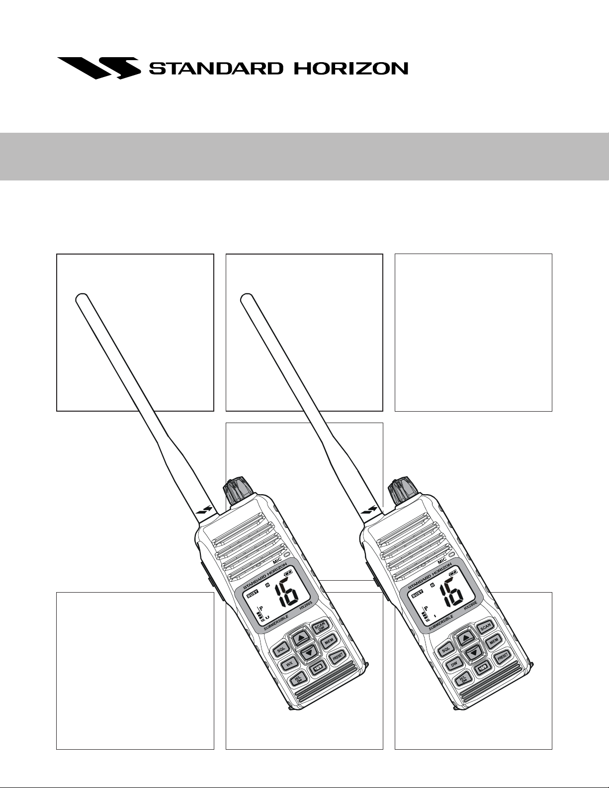
VHF FM Marine Transceiver
HX280S/E
SERVICE MANUAL
HX280S HX280E
EM038N90A
1
Page 2

Specifications (HX280S)
General
Frequency Ranges: TX: 156.025 MHz - 157.425 MHz
RX: 156.050 MHz - 163.275 MHz
Channel Spacing: 25 kHz
Frequency Stability: ±5 ppm (–4 °F to +140 °F [–20 °C to +60 °C])
Emission Type: 16K0G3E
Antenna Impedance: 50 Ω
Supply Voltage: 7.4V DC, Negative Ground (Battery Terminal)
Current Consumption: 320 mA (Receive, Typical at AF MAX.)
50 mA (Standby)
1.6 A / 0.7 A (TX: 5 W / 1W)
Operating Temperature: –4 °F to +140 °F (–20 °C to +60 °C)
Case Size (W x H x D): 2.20” x 5.24” x 1.08” (56 x 133 x 27.5 mm) w/o knob & antenna
Weight (Approx.): 10.9 oz (310 g) w/FNB-V105LI, Belt Clip, & Antenna
Transmitter
RF Power Output: 5 W / 1 W (@7.4 V )
Modulation Type: Variable Reactance
Maximum Deviation: ±5 kHz
Spurious Emission: –75 dBc typical
Microphone Impedance:2 kΩ
Receiver
Circuit Type: Double-Conversion Superheterodyne
Intermediate Frequencies: 1st: 21.7 MHz, 2nd: 450 kHz
Adjacent Channel Selectivity: 70 dB typical
Intermodulation: 68 dB typical
Hum & Noise Ratio: 40 dB typical
Sensitivity: 0.25 μV for 12 dB SINAD
Selectivity: 25 kHz (–70 dB)
AF Output (Internal SP): 700 mW @16 Ω for 10 % THD (@7.4 V)
Performance specifications are nominal, unless otherwise indicated, and are subject to change without notice.
Measured in accordance with TIA/EIA-603.
Important Note
The HX280S and HX280E was assembled using Pb (lead) free solder, based on the RoHS specification. Only lead-free solder (Alloy Composition: Sn-3.0Ag-0.5Cu) should be used for repairs performed on this apparatus. The solder stated above utilizes the alloy composition required for compliance with the lead-free specification, and any solder with the above alloy composition may be used.
2
Page 3

Specifications (HX280E)
General
Frequency Ranges: 156.025 MHz - 162.000 MHz
Channel Spacing: 25 kHz
Frequency Stability: ±5 ppm (–20 °C to +60 °C)
Emission Type: 16K0G3E
Antenna Impedance: 50 Ω
Supply Voltage: 7.4V DC, Negative Ground (Battery Terminal)
Current Consumption: 320 mA (Receive, Typical at AF MAX.)
50 mA (Standby)
1.6 A / 0.7 A (TX: 5 W / 1W)
Operating Temperature: –20 °C to +60 °C
Case Size (W x H x D): 56 x 133 x 27.5 mm (w/o knob & antenna)
Weight (Approx.): 310 g (w/FNB-V105LI, Belt Clip, & Antenna)
Transmitter
RF Power Output: 5 W / 1 W (@7.4 V )
Modulation Type: Variable Reactance
Maximum Deviation: ±5 kHz
Spurious Emission: Less than 0.25 μW
Microphone Impedance:2 kΩ
Receiver
Circuit Type: Double-Conversion Superheterodyne
Intermediate Frequencies: 1st: 21.7 MHz, 2nd: 450 kHz
Adjacent Channel Selectivity: 70 dB
Intermodulation: 68 dB
Hum & Noise Ratio: 40 dB
Sensitivity:1 μV for 20 dB SINAD
Selectivity: 25 kHz (–70 dB)
AF Output (Internal SP): 700 mW @16 Ω for 10 % THD (@7.4 V)
Performance specifications are nominal, unless otherwise indicated, and are subject to change without notice.
Measured in accordance with EN301 178-2, EN300 698-3, EN301 843-2, EN60950-1
3
Page 4
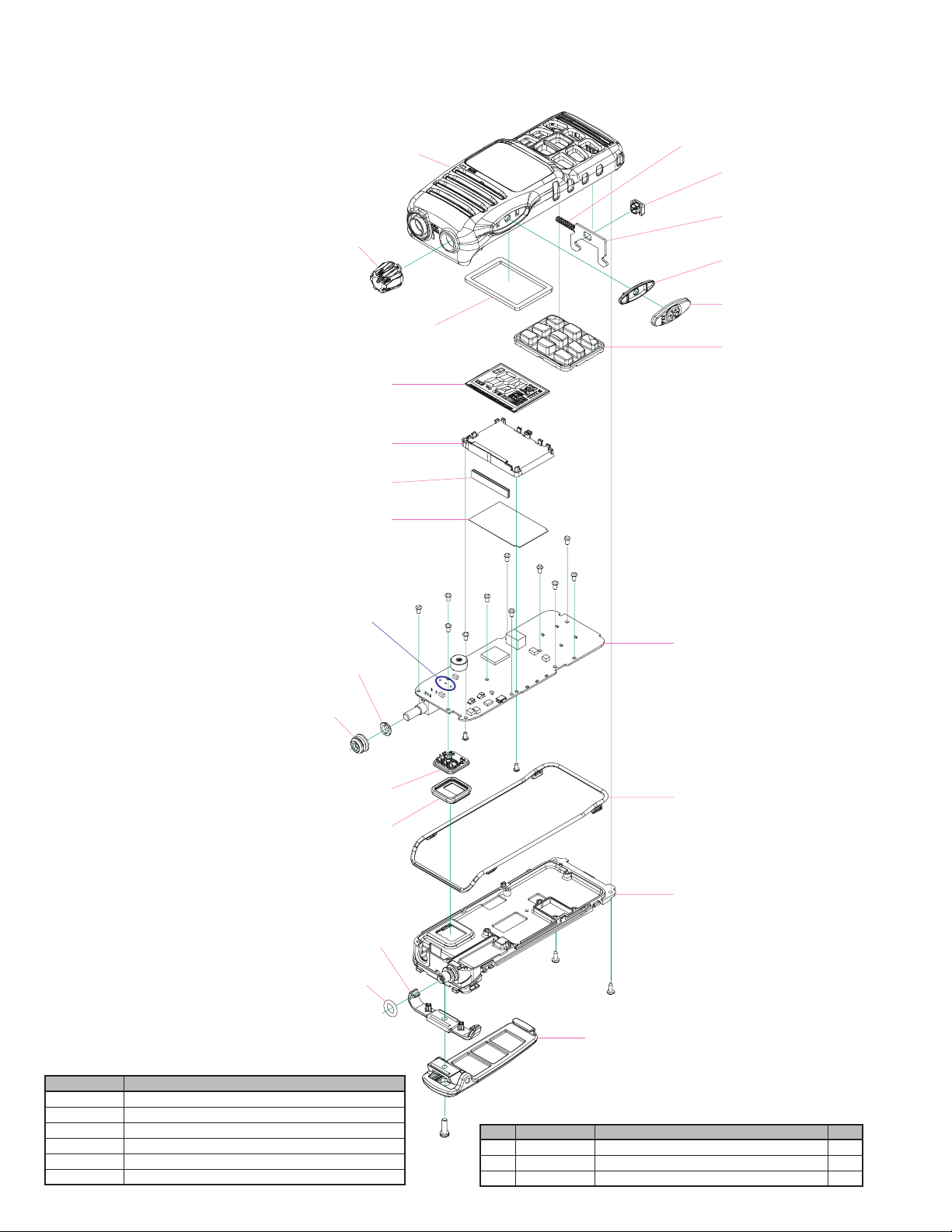
Exploded View & Miscellaneous Parts
CP9402001 (HX280S: USA)
CP9402002 (HX280S: EXP)
CP9402003 (HX280E: EU)
CP9402004 (HX280E: UK)
FRONT PANEL ASSY
RA0905300
COIL SPRING (C065)
RA1079100
LATCH NAIL
RA1078700
KNOB (VOL)
SPONGE RUBBER (WINDOW)
G6090189
RA1078900
LIGHT GUID (LCD)
RA1081000
INTER CONNECTOR (LCD)
RA1089600
REFLECTOR SHEET
Unsolder the three battery terminals
to remove the MAIN Unit
from the Rear Case
RA1079400
RING NUT (VOL)
RA1089500
LCD
e
e
e
e
e
e
e
e
e
RA1079200
LATCH PLATE
RA1078800
HOLDER (PTT)
RA1079600
RUBBER KNOB (PTT)
RA1080100 (HX280S)
RA1101200 (HX280E)
RUBBER KNOB
e
e
MAIN UNIT
VXSTD P/N
Q3000176
AAG43X001
Q9500142
Q9500143
Q9500144
CB4777001
4
RUBBER PACKING (VOL)
RA1079500
CS2020101
TERMINAL ASSY
RA1089600
RUBBER PACKING (TERMINAL)
RA1078500
CASE COVER (REAR)
RA091970
O RING (6x2.2)
DESCRIPTION
CAT460 Antenna
FNB-V105LI Li-Ion Battery Pack
NC-90B 120VAC Wall Charger (Type-A plug)
NC-90C 230VAC Wall Charger (Type-C plug)
NC-90U 230VAC Wall Charger (Type-BF plug)
CD-46 Charger Cradle
c
e
e
REF.
c
d
e
d
VXSTD P/N
U02310020
U24106020
U9900068
RA1079800
RUBBER PACKING (CASE)
CP9401001
REAR PANEL ASSY
d
CP9403001
BELT CLIP ASSY
Non-designated parts are available only
as part of a designated assembly.
DESCRIPTION
SEMS SCREW SM3X10SUS
BIND HEAD TAPTITE-B M2X6SUS
PAN HEAD TAPTITE-B M2X4NI#3
QTY.
1
2
13
Page 5
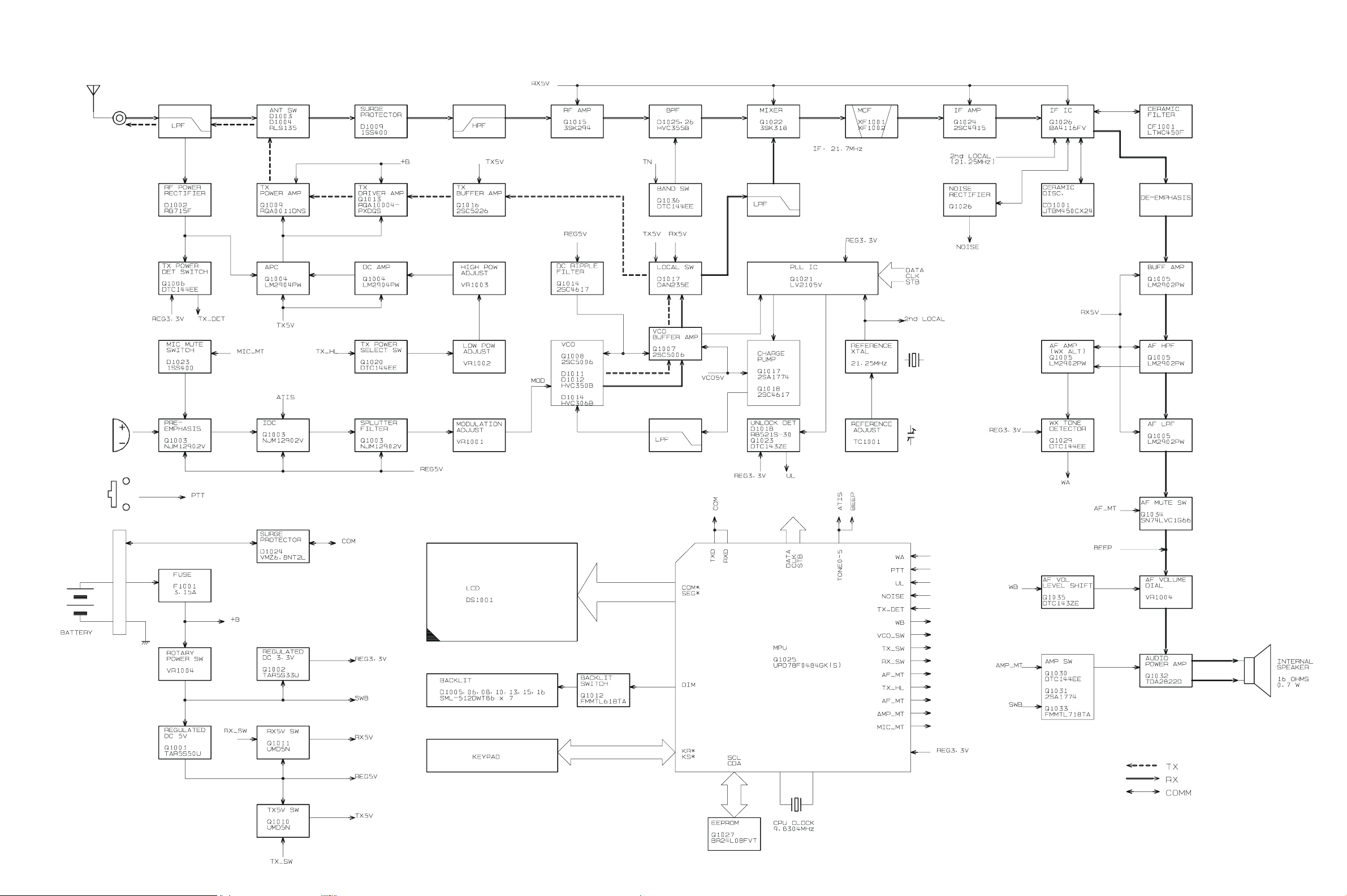
Block Diagram
5
Page 6

Note
6
Page 7

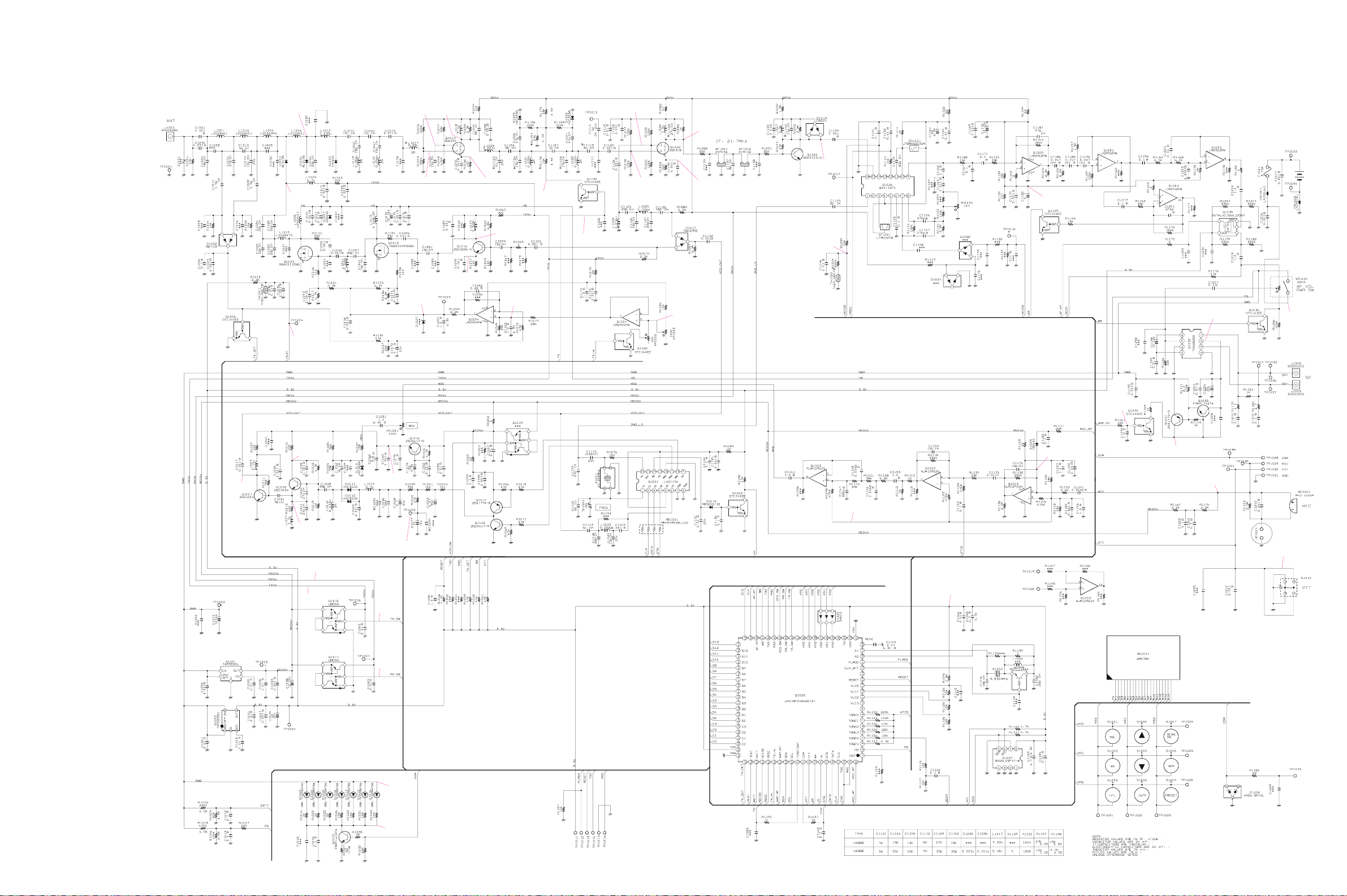
Circuit Description
1. Receive Signal Path
Incoming RF from the antenna jack passes through a lowpass filter consisting of coils L1001, L1002, & L1004, capacitors C1005, C1014, C1015, & C1019, and antenna
switching diode D1004 (RLS135).
Signals within the frequency range of the transceiver enter a band-pass filter consisting of coils L1013 and L1016,
capacitors C1060, C1064, and C1067, then amplified by
Q1015 and enter a Varactor-tuned band-pass filter consisting of coils L1021 & L1022, capacitors C1106, C1107,
C1108, C1120, & C1221, and diodes D1025 & D1026 (both
HVC355B), before first mixing by Q1022 (3SK318).
Buffered output from the VCO is amplified by Q1007
(2SC5006) to provide a pure first local signal between
134.35 and 141.575 MHz for injection to the first mixer
Q1022 (3SK318).
The 21.7 MHz first mixer product then passes through
monolithic crystal filter XF1001/XF1002 to strip away all
but the desired signal, which is then amplified by Q1024
(2SC4915). The amplified first IF signal is applied to FM
IF subsystem IC Q1026 (BA4116FV), which contains the
second mixer, second local oscillator, limited amplifier,
noise amplifier, and RSSI amplifier.
A second local signal is produced from the PLL reference/
second local oscillator of X1001 (21.25 MHz). The 21.25
MHz reference signal is delivered to mixer section of FM
IF subsystem IC Q1026 (BA4116FV) which produce the
450 kHz second IF mixed with the first IF signal.
The second IF then passes through the ceramic filter
CF1001 to strip away unwanted mixer products, and is
then applied to the limited amplifier in the FM IF subsystem IC Q1026 (BA4116FV), which removes amplitude
variations in the 450kHz IF, before detection of the speech
by the ceramic discriminator CD1001.
2. Audio Amplifier
The demodulated audio signal from the Q1026
(BA4116FV) passes through a band-pass filter and Highpass filter, then applied to the de-emphasis of Q1005
(LM2902PWR). Then passes through the audio mute
switch Q1034 (SN74LVC1G66DCKR), the audio volume
VR1004 and the audio power amplifier Q1032 (TDA2822)
pin 7, providing up to 700 mW of audio power to the 16ohm loudspeaker.
3. Squelch Control
The squelch circuitry consists of a noise amplifier and
band-pass filter and noise detector within Q1026
(BA4116FV). When no carrier received, noise at the output of the detector stage in Q1026 (BA4116FV) is ampli-
fied and band-pass filtered by the noise amplifier section
of Q1026 (BA4116FV) and the network between pins 7
and 8, and then rectified by detection circuit in Q1026
(BA4116FV).
The resulting DC squelch control voltage is passed to pin
64 of the microprocessor Q1025 (UPD78F0484GK). If no
carrier is received, this signal causes pin 38 of Q1025
(UPD78F0484GK) to go low and pin 67 to go high. Pin 67
signals of Q1025 (UPD78F0484GK) to disable the supply
voltage to the audio amplifier Q1032 (TDA2822).
Thus, the microprocessor blocks output from the audio
amplifier, and silences the receiver, while no signal is being received (and during transmission, as well).
4. Transmit Signal Path
The speech input from the microphone MC1001 passes
through the audio amplifier Q1003 (NJM12902V), which
is adjusted the microphone gain. The speech signal passes through pre-emphasis circuit to Q1003 (NJM12902V),
which contains the IDC, and low-pass filter. Then passes
through VR1001 which allows manual adjustment of the
transmitter deviation level.
The filtered audio signal is applied to varactor diode
D1014 (HVC306B), which frequency modulates the VCO
Q1008 (2SC5006).
The modulated signal from the VCO Q1008 (2SC5006) is
buffered by Q1007 (2SC5006). The low-level transmit sig-
nal is then passes through the TX switching diode D1017
(DAN235E) to the buffer amplifier Q1016 (2SC5226),
driver amplifier Q1013 (RQA0004PXDQS), then amplified transmit signal is applied to the final amplifier Q1009
(RQA0011DNS) up to 5.0 watts output power.
The transmit signal then passes through the antenna
switch D1003 (RLS135) and is low-pass filtered to suppress harmonic spurious radiation before delivery to the
antenna.
7
Page 8

Circuit Description
4-1 Automatic Transmit Power Control
Current from the final amplifier is sampled by C1011 &
C1022, and R1004 & R1008, and is rectified by D1002
(RB715F). The resulting DC is fed back through Q1004
(LM2904PWR) to the drive amplifier Q1013
(RQA0004PXDQS) and final amplifier Q1009
(RQA0011DNS), for control of the power output.
When the microprocessor selects “High” or “Low” power levels, pin 66 of Q1025 (UPD78F0484GK) to go low at
“High” power selected or pin 66 of Q1025
(UPD78F0484GK) to go high at “Low” power selected.
5. PLL Frequency Synthesizer
The PLL circuitry on the Main Unit consists of VCO Q1008
(2SC5006), VCO buffer Q1007 (2SC5006), PLL subsystem IC Q1021 (LV2105V), which contains a reference
divider, serial-to-parallel data latch, programmable divider, phase comparator and charge pump, and crystal X1001
which frequency stability is ±5 ppm @ –20 °C to +60 °C.
While receiving, VCO Q1008 (2SC5006) oscillates between 134.35 and 141.575 MHz according to the transceiver version and the programmed receiving frequency.
The VCO output is buffered by Q1007 (2SC5006), then
applied to the prescaler section of Q1021 (LV2105V). There
the VCO signal is divided by 64 or 65, according to a control signal from the data latch section of Q1021 (LV2105V),
before being sent to the programmable divider section of
Q1021 (LV2105V).
The data latch section of Q1021 (LV2105V) also receives
serial dividing data from the microprocessor Q1025, which
causes the pre-divided VCO signal to be further divided
in the programmable divider section, depending upon the
desired receive frequency, so as to produce a 25.0 kHz
derivative of the current VCO frequency.
Meanwhile, the reference divider sections of Q1021
(LV2105V) divides the 21.25 MHz crystal reference from
the reference oscillator section ofQ1021 (LV2105V), by 850
to produce the 25.0 kHz loops reference.
The 25.0 kHz signal from the programmable divider (derived from the VCO) and that derived from the reference
oscillator are applied to the phase detector section of
Q1021 (LV2105V), which produces a pulsed output with
pulse duration depending on the phase difference between
the input signals.
This pulse train is filtered to DC and returned to the Varactor D1011 and D1012 (both HVC350B).
Changes in the level of the DC voltage applied to the Varactor, affecting the reference in the tank circuit of the VCO
according to the phase difference between the signals
derived from the VCO and the crystal reference oscillator.
The VCO is thus phase-locked to the crystal reference oscillator. The output of the VCO Q1008 (2SC5006) after
buffering by Q1007 (2SC5006) is applied to the first mix-
er as described previously.
For transmission, the VCO Q1008 (2SC5006) oscillates
between 156.025 and 157.425 MHz according to the model version and programmed transmit frequency. The remainder of the PLL circuitry is shared with the receiver.
However, the dividing data from the microprocessor is
such that the VCO frequency is at the actual transmit frequency (rather than offset for IFs, as in the receiving case).
Also, the VCO is modulated by the speech audio applied
to D1014 (HVC306B), as described previously.
6. Miscellaneous Circuits
Push-To-Talk Transmit Activation
When the PTT switch on the Main Unit is closed, pin 72 of
Q1025 (UPD78F0484GK) goes low. This signal disables
the receiver by disabling the 5 V supply bus at Q1011
(UMD5N) to the front-end, FM IF subsystem IC Q1026
(BA4116FV).
At the same time, Q1010 (UMD5N) activate the transmit 5
V supply line to enable the transmitter.
8
Page 9

Alignment
The HX280S/E has been carefully aligned at the factory
for the specified performance across the marine band.
Realignment should therefore not be necessary except in
the event of a component failure.
All component replacement and service should be performed only by an authorized STANDARD HORIZON
representative, or the warranty policy may be voided.
The following procedures cover the sometimes critical and
tedious adjustments that are not normally required once
the transceiver has left the factory. However, if damage
occurs and some parts are replaced, realignment may be
required. If a sudden problem occurs during normal operation, it is likely due to component failure; realignment
should not be done until after the faulty component has
been replaced.
We recommend that servicing be performed only by authorized STANDARD HORIZON service technicians who
are experienced with the circuitry and fully equipped for
repair and alignment. Therefore, if a fault is suspected,
contact the dealer from whom the transceiver was purchased for instructions regarding repair. Authorized
STANDARD HORIZON service technicians realign all circuits and make complete performance checks to ensure
compliance with factory specifications after replacing any
faulty components. Those who do undertake any of the
following alignments are cautioned to proceed at their
own risk.
Problems caused by unauthorized attempts at realignment
are not covered by the warranty policy. Also, STANDARD
HORIZON must reserve the right to change circuits and
alignment procedures in the interest of improved performance, without notifying owners. Under no circumstances
should any alignment be attempted unless the normal
function and operation of the transceiver are clearly understood, the cause of the malfunction has been clearly
pinpointed and any faulty components replaced, and the
need for realignment determined to be absolutely necessary. The following test equipment (and thorough familiarity with its correct use) is necessary for complete realignment. Correction of problems caused by misalignment resulting from use of improper test equipment is
not covered under the warranty policy. While most steps
do not require all of the equipment listed, the interactions
of some adjustments may require that more complex adjustments be performed afterwards. Do not attempt to
perform only a single step unless it is clearly isolated electrically from all other steps. Have all test equipment ready
before beginning, and follow all of the steps in a section
in the order presented.
Required Test Equipment
RF Signal Generator with calibrated output level at
200 MHz
Frequency Counter: >0.1 ppm accuracy at 200 MHz
AF Signal Generator
Deviation Meter (linear detector)
VHF Sampling Coupler
Inline Wattmeter with 5% accuracy at 200 MHz
50-ohm Non-reactive Dummy Load: 10W at 200 MHz
7.4 VDC, 2A Regulated DC Power Supply
IBM® PC/compatible computer with Microsoft® Win-
dows® 2000, XP, or Vista
Standard Horizon HX280 Service Flag Controller and
Alignment Jig.
Alignment Preparation & Precautions
A dummy load and inline wattmeter must be connected
to the main antenna jack in all procedures that call for
transmission, except where specified otherwise. Correct
alignment is not possible with an antenna. After completing one step, read the following step to determine whether the same test equipment will be required. If not, remove the test equipment (except dummy load and wattmeter, if connected) before proceeding.
Correct alignment requires that the ambient temperature
be the same as that of the transceiver and test equipment,
and that this temperature be held constant between 20 °C
and 30 °C (68 °F ~ 86 °F). When the transceiver is brought
into the shop from hot or cold air it should be allowed
some time for thermal equalization with the environment
before alignment. If possible, alignments should be made
with oscillator shields and circuit boards firmly affixed
in place. Also, the test equipment must be thoroughly
warmed up before beginning.
Note: Signal levels in dB referred to in this procedure are
based on 0 dBμ = 0.5 μV(closed circuit).
9
Page 10
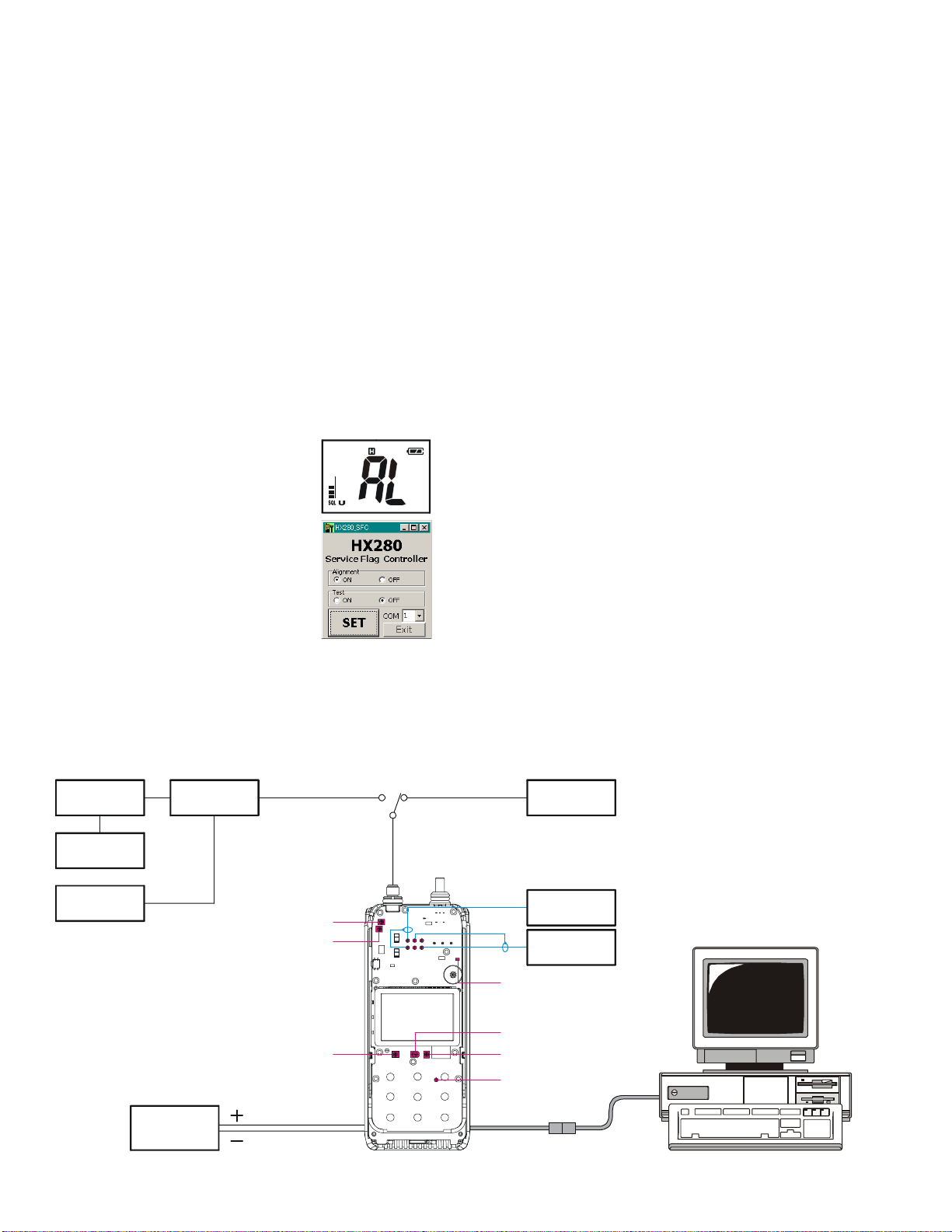
Alignment
Before Alignment
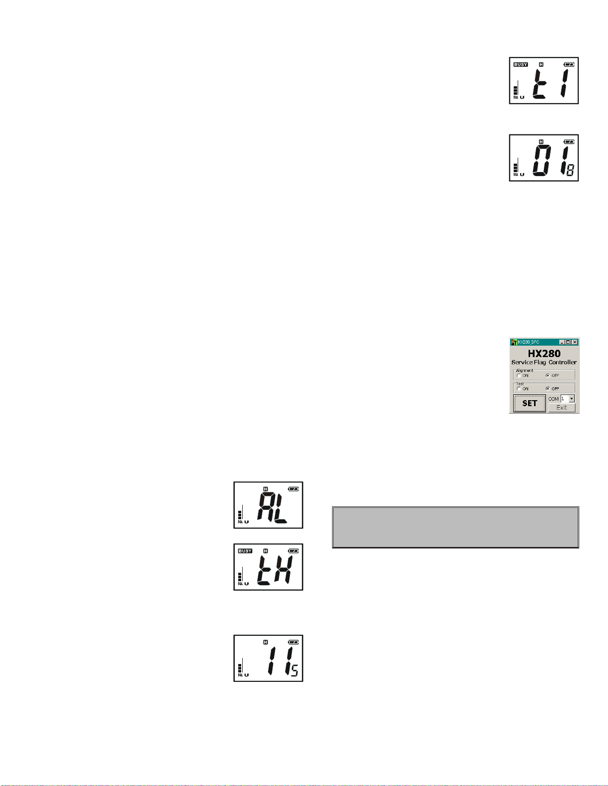
Install the HX280 Service Flag Controller Program to
your computer.
Remove the Front Panel from the transceiver accord-
ing to the following procedures:
1) Disconnect the antenna from the transceiver.
2) Remove the VOL knob and Battery Pack from the
transceiver
3) Remove the two screws which located at the bottom side on the battery compartment.
4) Carefully pull out the chassis from the Front Panel.
Refer to the “Exploded View“ on the page 4.
Set up the test equipment as shown below, and set the
DC Power Supply voltage to 7.4 V.
Execute the HX280 Service Flag Controller Program.
Select the COM port number which is connected to
the HX280 Alignment Jig.
Press and hold in the [PRESET] key
while turning the transceiver on to
enter the Alignment Mode.
Select “Alignment ON” Radio But-
ton of the HX280 Service Flag Controller Program.
Click the left mouse button on the
[
SET] button of the HX280 Service
Flag Controller Program.
Main Reference Frequency Adjustment
Turn the Antenna switch to the “TX Alignment” side.
Remove the solder jumper JP1001.
Set the channel to CH16.
Use the [H/L] key to set the transceiver to “LOW”
power.
With the PTT switch pressed, adjust TC1001 so the
Frequency Counter reading is 156.800 MHz ± 100 Hz.
Transmit Power Adjustment
Turn the Antenna switch to the “TX Alignment” side.
Set the channel to CH16.
Increase the DC Power Supply voltage to 8.0 V.
Use the [H/L] key to set the transceiver to “HI” power.
With the PTT switch pressed, adjust VR1003 so that
RF output power is 5.0 W ± 0.1 W.
Release the PTT switch, then set the transceiver to
“LOW” power by the [H/L] key.
With the PTT switch pressed, adjust VR1002 so that
RF output power is 0.8 W ± 0.1 W.
Release the PTT switch.
Return the DC Power Supply voltage to 7.4 V.
Inline
Wattmeter
50
Dummy Load
Frequency
Counter
10
Ω
Power Supply
RF Sampling
Coupler
Regulated
( ) :
( ) :
( ) :
( ) :
VR1002
VR1003
VR1001
RED
RED
BLACK
BLACK
Antenna Switch
“RX” Alignment“TX” Alignment
HX280 Alignment Jig
RF Signal
Generator
Attention!
The HX280’s Audio output is BTL output.
16 1 W
Ω
Resistor
AF Signal
Generator
JP1001
TC1001
VR1005
TP1018
D-SUB 9-pin Jack
Page 11
Alignment
TX Deviation Adjustment
Turn the Antenna switch to the “TX Alignment” side.
Confirm that the solder jumper JP1001 is removed.
Set the AF Signal Generator output to 200 mVrms at 1
kHz.
Set the channel to CH16.
With the PTT switch pressed, adjust VR1001 so that
the maximum deviation is 4.4 kHz ± 0.1 kHz.
Release the PTT switch.
Solder the jumper JP1001.
Squelch Level Adjustment
Turn the Antenna switch to the “RX Alignment” side.
Set the channel to CH16.
Set the RF Signal Generator output to 156.800 MHz,
at a level of +0 dBμ (HX280S) or +3 dBμ (HX280E),
±3.0 kHz deviation with a 1 kHz audio tone.
Connect the DC voltmeter to TP1018, adjust VR1005
so that DC voltmeter reading is 0.2 V ± 0.02 V (HX280S)
or 0.45 V ± 0.02 V (HX280E).
Software Alignment/Confirmation Mode
Overview of Software Alignment Mode
The “Software Alignment Mode” has been build in
the microprocessor in order to adjust and confirm the
performance of transceiver.
The purpose is to adjust transceiver simply and to con-
firm the performance of transceiver smoothly.
Starting Software Alignment Mode
Set the channel to CH16, then turn the VOL knob
counter clockwise to turn off the radio.
Turn the Antenna switch to the “RX Alignment” side.
Turn the VOL knob clockwise to
turn on the radio while press and
holding the [PRESET] keys. The
LCD will be shown the Alignment
mode “
Press the [SCAN] key. Then the LCD
will be shown the Alignment Item
(1st Item is Threshold “
Set the RF Signal Generator output
to 156.800 MHz, at a level of –8 dBμ (HX280S) or
–6 dBμ (HX280E), ±3.0 kHz deviation with a 1 kHz
audio tone.
Press the [PRESET] key to record a
threshold level.
Press the [MEM] key to save the new
setting.
ALAL
AL”.
ALAL
tHtH
tH”).
tHtH
Press the [SCAN] key to recall the
Alignment Item “
Set the RF Signal Generator output
to 156.800 MHz, at a level of +0 dBμ
(HX280S) or +3 dBμ (HX280E), ±3.0 kHz deviation
with a 1 kHz audio tone.
Press the [PRESET] key to record a
tight level.
Press the [MEM] key to save the new
setting.
This completes the Software Alignment Mode. To save
all settings and exit, press and hold the [16/9] key for one
second. Then turn off the transceiver.
tI tI
tI (TIGHT)”.
tI tI
After Alignment
Execute the HX280 Service Flag Controller Program
again.
Select the COM port number which is connected to
the HX280 Alignment Jig.
Press and hold in the [PRESET] key while turning
the transceiver on to enter the Alignment Mode.
Select “Alignment OFF” Radio But-
ton of HX280 Service Flag Controller Program.
Click the left mouse button on the
[
SET] button of the HX280 Service
Flag Controller Program.
Turn off the transceiver.
Assemble the transceiver while being carefully so that
Rubber Packing does not protrude from a Front Case.
Important Note: To ensure the radio is water proof,
make sure the gasket is installed on the chassis correctly and is not pinched when inserted into the front
case.
NOTICE
Do not touch the Alignment Item “
dCdC
dC”.
dCdC
11
Page 12

Note
12
Page 13
MAIN Unit
RX: 0 V
TX: 0.82 V
RX: 0 V
TX: 1.66 V
3.11 V
RX: 3.53 V
TX: 0 V
RX: 2.48 V
TX: 0 V
RX: 0 V
TX: 1.13 V
RF AMP
Q1015
RX: 4.18 V
TX: 0 V
RX: 0 V
TX: 0.91 V
RX: 1.09 V
TX: 0 V
RX: 0 V
TX: 2.83 V
BPF “LOW”: 0.01 V
BPF “HIGH”: 1.56 V
RX: 0 V
TX: 1.41 V
BPF “LOW”: 3.29 V
BPF “HIGH”: 0 V
RX: 2.54 V
TX: 0 V
RX: 2.33 V
TX: 0 V
VCO Input
1st Mixer
Q1022
RX: 0 V
TX: 2.21 V
RX: 4.67 V
TX: 0 V
RX: 3.92 V
TX: 0 V
IF AMP
Q1024
RX: 1.82 V
TX: 0 V
RX SIGNAL “Non”: 1.15 V
RX SIGNAL “40 dBμ”: 0.02 V
2nd Mixer / IF
Q1026
RX: 1.75 V
TX: 0 V
RX: 2.77 V
TX: 0 V
Circuit Diagram
RX: 7.35 V
TX: 0.40 V
7.40 V
2.28 V
3.44 V
1.93 V
RX: 0 V
TX: 4.78 V
RX: 4.90 V
TX: 0 V
4.12 V
RX: 0 V
TX: 3.29 V
RX: 3.29 V
TX: 0 V
RX: 1.69 V
TX: 3.37 V
1.78 V
3.30 V
RX: 2.75 V
TX: 1.84 V
RX: 6.62 V
TX: 7.12 V
RX: 1.41 V
TX: 1.41 V
RX: 3.29 V
TX: 0 V
7.39 V
0 V
13
Page 14

MAIN Unit
Note
14
Page 15

MAIN Unit
Parts Layout (Side A)
BA DC FE G
H
1
2
3
4
μPD78F0484GK
(Q1025)
LM2904PWR
(Q1004)
DTC143ZE (E23)
(Q1035)
DTC144EE (26)
(Q1020, 1036)
VMZ6.8NT2L (6C)
(D1024)
15
Page 16

MAIN Unit
Parts Layout (Side B)
ba dc fe
g
h
1
2
3
4
BA4116FV
(Q1026)
LV2105V
(Q1021)
LM2902PWR
(Q1005)
NJM12902V
(Q1003)
BR24L08FVT
(Q1027)
2SA1774 (FR)
(Q1017, 1031)
FMMTL718TA
(Q1033)
2SC4617 (BR)
(Q1014, 1018)
2SC4915 (QY)
(Q1024)
2SC5006 (24)
(Q1007, 1008)
2SC5226 (R22)
(Q1016)
3SK294 (UV)
(Q1022)
3SK318 (YB)
(Q1022)
DTC144EE (26)
(Q1006, 1029,
1030)
RQA0004PXDQS (PX)
(Q1013)
SN74LVC1G66
(Q1034)
UMD5N
(Q1010, 1011)
DA221 (K)
(D1019)
IMN10 (N10)
(D1020)
16
TDA2822D013TR
(Q1032)
DTC143ZE (E23)
(Q1023)
FMMTL618TA (L68)
(Q1012)
RQA0011DNS
(Q1009)
TAR5S33U
(Q1002)
TAR5S50U
(Q1001)
DAN235E
(D1017)
RB715F (3D)
(D1002)
Page 17

MAIN Unit
Parts List
REF DESCRIPTION VALUE V/W TOL. MFR'S DESIG VXSTD P/N VERS.
PCB with Components (No adjustment. Requires the adjustment for use.) CB4645001 HX280S
CB4645002 HX280E
Printed Circuit Board FR019200C 1C 1001 CHIP CAP. 0.001uF 50V B GRM155B11H102KA01D K22178809 1- B h3
C 1004 CHIP CAP. 0.1uF 10V B GRM155B11A104KA01D K22108802 1- B h3
C 1005 CHIP CAP. 18pF 50V CH GRM1552C1H180JZ01D K22178218 1- B h3
C 1006 CHIP CAP. 0.001uF 50V B GRM155B11H102KA01D K22178809 1- B g1
C 1007 CHIP CAP. 0.01uF 25V B GRM155B11E103KA01D K22148834 1- B f1
C 1009 CHIP CAP. 0.001uF 50V B GRM155B11H102KA01D K22178809 1- B h3
C 1010 CHIP TA.CAP. 10uF 16V TEESVA1C106M8R K78120077 1- A A2
C 1011 CHIP CAP. 0.5pF 50V CK UMK105CK0R5CV-F K22178247 1- B h3
C 1012 CHIP CAP. 0.1uF 10V B GRM155B11A104KA01D K22108802 1- B e2
C 1013 CHIP CAP. 0.1uF 10V B GRM155B11A104KA01D K22108802 1- B e1
C 1014 CHIP CAP. 27pF 50V CH GRM1552C1H270JZ01D K22178222 1- B h3
C 1015 CHIP CAP. 4pF 25V CH TMK105CH040C-F K22148208 1- B g3
C 1017 CHIP CAP. 0.001uF 50V B GRM155B11H102KA01D K22178809 1- B c3
C 1018 CHIP CAP. 0.01uF 25V B GRM155B11E103KA01D K22148834 1- B g1
C 1019 CHIP CAP. 10pF 25V CH TMK105CH100D-F K22148214 1- B g3
C 1020 CHIP CAP. 0.01uF 25V B GRM155B11E103KA01D K22148834 1- B g1
C 1021 CHIP CAP. 0.01uF 25V B GRM155B11E103KA01D K22148834 1- B g1
C 1022 CHIP CAP. 0.5pF 50V CK UMK105CK0R5CV-F K22178247 1- B g3
C 1024 CHIP CAP. 18pF 50V CH GRM1552C1H180JZ01D K22178218 1- B g3
C 1025 CHIP CAP. 18pF 50V CH GRM1552C1H180JZ01D K22178218 1- B f3
C 1026 CHIP CAP. 0.01uF 25V B GRM155B11E103KA01D K22148834 1- B g2
C 1027 CHIP CAP. 0.001uF 50V B GRM155B11H102KA01D K22178809 1- B g1
C 1028 CHIP CAP. 56pF 50V CH GRM1552C1H560JD01D K22178230 1- B g3
C 1029 CHIP CAP. 33pF 50V CH GRM1552C1H330JZ01D K22178224 1- B f3
C 1030 CHIP CAP. 0.01uF 25V B GRM155B11E103KA01D K22148834 1- B f3
C 1031 CHIP CAP. 5pF 25V CH TMK105CH050C-F K22148209 1- B c3
C 1033 CHIP CAP. 0.001uF 50V B GRM155B11H102KA01D K22178809 1- B g2
C 1034 CHIP TA.CAP. 10uF 10V TEESVA1A106M8R K78100028 1- A B1
C 1035 CHIP CAP. 0.001uF 50V B GRM155B11H102KA01D K22178809 1- B c3
C 1036 CHIP CAP. 0.001uF 50V B GRM155B11H102KA01D K22178809 1- B f3
C 1038 CHIP TA.CAP. 10uF 10V TEESVA1A106M8R K78100028 1- A B1
C 1039 CHIP CAP. 0.001uF 50V B GRM155B11H102KA01D K22178809 1- B c3
C 1040 CHIP CAP. 27pF 50V CH GRM1552C1H270JZ01D K22178222 1- B c3
C 1041 CHIP CAP. 27pF 50V CH GRM1552C1H270JZ01D K22178222 1- B c3
C 1043 CHIP CAP. 0.001uF 50V B GRM155B11H102KA01D K22178809 1- B f3
C 1044 CHIP CAP. 0.001uF 50V B GRM155B11H102KA01D K22178809 1- B f3
C 1045 CHIP CAP. 22pF 50V CH UMK105CH220JV-F K22178266 1- B g3
C 1046 CHIP CAP. 0.1uF 10V B GRM155B11A104KA01D K22108802 1- B a3
C 1047 CHIP CAP. 0.01uF 25V B GRM155B11E103KA01D K22148834 1- B f3
C 1048 CHIP CAP. 33pF 50V CH GRM1552C1H330JZ01D K22178224 1- B c3
C 1049 CHIP CAP. 0.001uF 50V B GRM155B11H102KA01D K22178809 1- A C3
C 1050 CHIP CAP. 0.001uF 50V B GRM155B11H102KA01D K22178809 1- A C3
C 1052 CHIP CAP. 1pF 25V CK TMK105CK010C-F K22148205 1- B c3
C 1054 CHIP CAP. 0.001uF 50V B GRM155B11H102KA01D K22178809 1- B f3
C 1055 CHIP CAP. 15pF 25V CH TMK105CH150J-F K22148218 1- B g2
C 1056 CHIP CAP. 0.001uF 50V B GRM155B11H102KA01D K22178809 1- A C3
C 1057 CHIP CAP. 82pF 50V CH GRM1552C1H820JD01D K22178234 1- B e3
C 1058 CHIP CAP. 0.001uF 50V B GRM155B11H102KA01D K22178809 1- A C3
C 1060 CHIP CAP. 18pF 50V CH GRM1552C1H180JZ01D K22178218 1- B g2
C 1061 CHIP CAP. 15pF 25V CH TMK105CH150J-F K22148218 1- B e3
C 1062 CHIP CAP. 0.001uF 50V B GRM155B11H102KA01D K22178809 1- B c3
C 1063 CHIP CAP. 0.01uF 25V B GRM155B11E103KA01D K22148834 1- B f1
C 1064 CHIP CAP. 15pF 25V CH TMK105CH150J-F K22148218 1- B g2
C 1065 CHIP CAP. 0.01uF 25V B GRM155B11E103KA01D K22148834 1- B f1
C 1066 CHIP CAP. 2.2uF 10V B GRM188B31A225KE18D K22104805 1- B c3
C 1067 CHIP CAP. 33pF 50V CH GRM1552C1H330JZ01D K22178224 1- B g2
C 1068 CHIP TA.CAP. 0.1uF 35V TEESVA1V104M8R K78160025 1- B d3
C 1069 CHIP CAP. 0.001uF 50V B GRM155B11H102KA01D K22178809 1- B c2
C 1070 CHIP TA.CAP. 10uF 16V TEESVA1C106M8R K78120077 1- B g3
C 1071 CHIP CAP. 0.001uF 50V B GRM155B11H102KA01D K22178809 1- B e3
C 1072 CHIP CAP. 0.1uF 10V B GRM155B11A104KA01D K22108802 1- A A3
C 1073 CHIP CAP. 0.001uF 50V B GRM155B11H102KA01D K22178809 1- B g2
C 1074 CHIP CAP. 0.001uF 50V B GRM155B11H102KA01D K22178809 1- B e3
C 1075 CHIP CAP. 0.1uF 10V B GRM155B11A104KA01D K22108802 1- B c2
C 1076 CHIP CAP. 0.01uF 25V B GRM155B11E103KA01D K22148834 1- B e3
C 1077 CHIP TA.CAP. 10uF 10V TEESVA1A106M8R K78100028 1- B d3
C 1079 CHIP TA.CAP. 22uF 6.3V TEESVA0J226M8R K78080047 1- B c3
C 1081 CHIP CAP. 15pF 25V CH TMK105CH150J-F K22148218 1- B e3
C 1082 CHIP CAP. 0.001uF 50V B GRM155B11H102KA01D K22178809 1- B c3
C 1083 CHIP TA.CAP. 0.47uF 35V TEESVA1V474M8R K78160029 1- B d3
LOT
SIDE
LAY ADR
17
Page 18

MAIN Unit
Parts List
REF DESCRIPTION VALUE V/W TOL. MFR'S DESIG VXSTD P/N VERS.
C 1084 CHIP CAP. 1uF 6.3V B GRM155B30J105KE18D K22088803 1- B d1
C 1086 CHIP CAP. 10pF 25V CH TMK105CH100D-F K22148214 1- B g2
C 1087 CHIP CAP. 1uF 6.3V B GRM155B30J105KE18D K22088803 1- A C3
C 1088 CHIP CAP. 0.01uF 25V B GRM155B11E103KA01D K22148834 1- B c3
C 1089 CHIP CAP. 0.001uF 50V B GRM155B11H102KA01D K22178809 1- B e3
C 1090 CHIP CAP. 0.001uF 50V B GRM155B11H102KA01D K22178809 1- B e3
C 1091 CHIP CAP. 0.001uF 50V B GRM155B11H102KA01D K22178809 1- B g2
C 1092 CHIP CAP. 0.22uF 10V B GRM155B31A224KE18D K22108808 1- A B3
C 1093 CHIP CAP. 0.1uF 10V B GRM155B11A104KA01D K22108802 1- B d3
C 1094 CHIP CAP. 8pF 50V CH GRM1552C1H8R0DZ01D K22178210 1- B g2
C 1095 CHIP CAP. 0.001uF 50V B GRM155B11H102KA01D K22178809 1- B d3
C 1097 CHIP CAP. 0.01uF 25V B GRM155B11E103KA01D K22148834 1- B f1
C 1098 CHIP CAP. 0.001uF 50V B GRM155B11H102KA01D K22178809 1- B g2
C 1099 CHIP CAP. 10pF 25V CH TMK105CH100D-F K22148214 1- B e3
C 1100 CHIP CAP. 6pF 50V CH GRM1552C1H6R0DZ01D K22178208 HX280E 1- B g2
C 1100 CHIP CAP. 4pF 25V CH TMK105CH040C-F K22148208 HX280S 1- B g2
C 1102 CHIP CAP. 1uF 6.3V B GRM155B30J105KE18D K22088803 1- A B3
C 1104 CHIP CAP. 8pF 50V CH GRM1552C1H8R0DZ01D K22178210 1- B g2
C 1105 CHIP CAP. 0.001uF 50V B GRM155B11H102KA01D K22178809 1- B e3
C 1106 CHIP CAP. 12pF 25V CH TMK105CH120J-F K22148216 HX280E 1- B f2
C 1106 CHIP CAP. 13pF 50V CH UMK105CH130JV-F K22178261 HX280S 1- B f2
C 1107 CHIP CAP. 1pF 25V CK TMK105CK010C-F K22148205 1- B f2
C 1108 CHIP CAP. 12pF 25V CH TMK105CH120J-F K22148216 HX280E 1- B f2
C 1108 CHIP CAP. 13pF 50V CH UMK105CH130JV-F K22178261 HX280S 1- B f2
C 1109 CHIP CAP. 27pF 50V CH GRM1552C1H270JZ01D K22178222 1- B c2
C 1110 CHIP CAP. 3pF 25V CJ TMK105CJ030C-F K22148207 1- B c2
C 1111 CHIP CAP. 1pF 25V CK TMK105CK010C-F K22148205 1- B f2
C 1112 CHIP CAP. 4pF 25V CH TMK105CH040C-F K22148208 HX280E 1- B f2
C 1112 CHIP CAP. 8pF 50V CH GRM1552C1H8R0DZ01D K22178210 HX280S 1- B f2
C 1113 CHIP CAP. 5pF 25V CH TMK105CH050C-F K22148209 1- B d3
C 1114 CHIP CAP. 1uF 6.3V B GRM155B30J105KE18D K22088803 1- A B3
C 1115 CHIP CAP. 100pF 25V CH TMK105CH101J-F K22148238 1- B c2
C 1116 CHIP CAP. 0.001uF 50V B GRM155B11H102KA01D K22178809 1- A B3
C 1118 CHIP CAP. 68pF 50V CH GRM1552C1H680JZ01D K22178232 1- B d3
C 1119 CHIP CAP. 0.01uF 25V B GRM155B11E103KA01D K22148834 1- B e2
C 1120 CHIP CAP. 0.001uF 50V B GRM155B11H102KA01D K22178809 1- B f2
C 1121 CHIP CAP. 15pF 25V CH TMK105CH150J-F K22148218 1- B d3
C 1122 CHIP CAP. 0.001uF 50V B GRM155B11H102KA01D K22178809 1- B e2
C 1123 CHIP CAP. 0.001uF 50V B GRM155B11H102KA01D K22178809 1- B d3
C 1124 CHIP CAP. 0.001uF 50V B GRM155B11H102KA01D K22178809 1- B f2
C 1125 CHIP CAP. 22pF 50V CH UMK105CH220JV-F K22178266 1- B e2
C 1126 CHIP CAP. 18pF 50V CH GRM1552C1H180JZ01D K22178218 1- B e3
C 1127 CHIP CAP. 22pF 50V CH UMK105CH220JV-F K22178266 1- B e3
C 1128 CHIP CAP. 18pF 50V CH GRM1552C1H180JZ01D K22178218 1- B e3
C 1129 CHIP CAP. 33pF 50V CH GRM1552C1H330JZ01D K22178224 HX280E 1- B e2
C 1129 CHIP CAP. 27pF 50V CH GRM1552C1H270JZ01D K22178222 HX280S 1- B e2
C 1130 CHIP CAP. 0.001uF 50V B GRM155B11H102KA01D K22178809 1- B f2
C 1131 CHIP CAP. 0.01uF 25V B GRM155B11E103KA01D K22148834 1- B d3
C 1132 CHIP CAP. 0.001uF 50V B GRM155B11H102KA01D K22178809 1- B e3
C 1134 CHIP CAP. 0.1uF 10V B GRM155B11A104KA01D K22108802 1- B d3
C 1135 CHIP CAP. 0.001uF 50V B GRM155B11H102KA01D K22178809 1- B d3
C 1136 CHIP CAP. 0.1uF 10V B GRM155B11A104KA01D K22108802 1- B d3
C 1137 CHIP CAP. 8pF 50V CH GRM1552C1H8R0DZ01D K22178210 1- B e2
C 1139 CHIP CAP. 0.01uF 25V B GRM155B11E103KA01D K22148834 1- B d2
C 1141 CHIP CAP. 1uF 6.3V B GRM155B30J105KE18D K22088803 1- B b3
C 1142 CHIP CAP. 33pF 50V CH GRM1552C1H330JZ01D K22178224 HX280E 1- B d2
C 1142 CHIP CAP. 15pF 25V CH TMK105CH150J-F K22148218 HX280S 1- B d2
C 1143 CHIP CAP. 0.1uF 10V B GRM155B11A104KA01D K22108802 1- A D3
C 1144 CHIP CAP. 0.001uF 50V B GRM155B11H102KA01D K22178809 1- B b2
C 1145 CHIP CAP. 2pF 50V CK GRM1554C1H2R0CZ01D K22178204 1- B c2
C 1146 CHIP CAP. 0.01uF 25V B GRM155B11E103KA01D K22148834 1- B b1
C 1147 CHIP CAP. 330pF 50V B UMK105B331KW-F K22178823 1- B b3
C 1148 CHIP CAP. 0.0056uF 25V B TMK105B562KW-F K22148832 1- B b3
C 1149 CHIP CAP. 0.47uF 6.3V B GRM155B30J474KE18D K22088802 1- A E1
C 1150 CHIP CAP. 0.0068uF 25V B TMK105B682KW-F K22148833 1- B b3
C 1151 CHIP CAP. 0.1uF 10V B GRM155B11A104KA01D K22108802 1- B b1
C 1152 CHIP CAP. 0.01uF 25V B GRM155B11E103KA01D K22148834 1- B b1
C 1153 CHIP CAP. 1uF 6.3V B GRM155B30J105KE18D K22088803 1- B b3
C 1154 CHIP CAP. 82pF 50V CH GRM1552C1H820JD01D K22178234 1- B c2
C 1155 CHIP CAP. 0.1uF 10V B GRM155B11A104KA01D K22108802 1- B c1
C 1156 CHIP CAP. 270pF 50V B UMK105B271KW-F K22178822 1- B c1
C 1157 CHIP CAP. 270pF 50V B UMK105B271KW-F K22178822 1- B c1
C 1159 CHIP CAP. 15pF 25V CH TMK105CH150J-F K22148218 1- B a3
LOT
SIDE
LAY ADR
18
Page 19

MAIN Unit
Parts List
REF DESCRIPTION VALUE V/W TOL. MFR'S DESIG VXSTD P/N VERS.
C 1160 CHIP CAP. 0.1uF 10V B GRM155B11A104KA01D K22108802 1- B h1
C 1161 CHIP TA.CAP. 22uF 6.3V TEESVA0J226M8R K78080047 1- B c1
C 1162 CHIP CAP. 0.1uF 10V B GRM155B11A104KA01D K22108802 1- B b1
C 1163 CHIP CAP. 0.001uF 50V B GRM155B11H102KA01D K22178809 1- B b1
C 1164 CHIP CAP. 0.01uF 25V B GRM155B11E103KA01D K22148834 1- B c1
C 1165 CHIP CAP. 0.1uF 10V B GRM155B11A104KA01D K22108802 1- B a3
C 1166 CHIP CAP. 0.01uF 25V B GRM155B11E103KA01D K22148834 1- A E1
C 1167 CHIP CAP. 0.1uF 10V B GRM155B11A104KA01D K22108802 1- B b1
C 1168 CHIP CAP. 4.7uF 6.3V B C1608JB0J475KT K22084804 1- A E1
C 1169 CHIP CAP. 0.001uF 50V B GRM155B11H102KA01D K22178809 1- B b1
C 1171 CHIP CAP. 0.1uF 10V B GRM155B11A104KA01D K22108802 1- B b1
C 1172 CHIP TA.CAP. 10uF 10V TEESVA1A106M8R K78100028 1- B b1
C 1174 CHIP CAP. 18pF 50V CH GRM1552C1H180JZ01D K22178218 1- B d1
C 1175 CHIP CAP. 0.047uF 16V F GRM155F11C473ZA01D K22129004 1- B a3
C 1176 CHIP CAP. 15pF 25V CH TMK105CH150J-F K22148218 1- B a3
C 1177 CHIP CAP. 0.001uF 50V B GRM155B11H102KA01D K22178809 1- B b2
C 1180 CHIP TA.CAP. 4.7uF 16V TEESVA1C475M8R K78120031 1- B b2
C 1181 CHIP CAP. 47pF 50V CH GRM1552C1H470JZ01D K22178228 1- B b1
C 1182 CHIP CAP. 22pF 50V CH UMK105CH220JV-F K22178266 1- B d1
C 1183 CHIP CAP. 4.7uF 6.3V B C1608JB0J475KT K22084804 1- B e1
C 1184 CHIP CAP. 0.01uF 25V B GRM155B11E103KA01D K22148834 1- B e1
C 1185 CHIP CAP. 0.1uF 10V B GRM155B11A104KA01D K22108802 1- B b3
C 1186 CHIP CAP. 0.047uF 10V B GRM155B11A473KA01D K22108801 1- B a1
C 1187 CHIP CAP. 1uF 6.3V B GRM155B30J105KE18D K22088803 1- B b3
C 1188 CHIP CAP. 0.047uF 10V B GRM155B11A473KA01D K22108801 1- B a1
C 1189 CHIP CAP. 0.001uF 50V B GRM155B11H102KA01D K22178809 1- B b3
C 1190 CHIP CAP. 0.001uF 50V B GRM155B11H102KA01D K22178809 1- B b3
C 1191 CHIP CAP. 0.0056uF 25V B TMK105B562KW-F K22148832 1- B a3
C 1192 CHIP CAP. 0.047uF 10V B GRM155B11A473KA01D K22108801 1- B a1
C 1193 CHIP CAP. 1uF 6.3V B GRM155B30J105KE18D K22088803 1- B b3
C 1194 CHIP CAP. 1uF 6.3V B GRM155B30J105KE18D K22088803 1- B g2
C 1195 CHIP CAP. 0.001uF 50V B GRM155B11H102KA01D K22178809 1- B h1
C 1196 CHIP CAP. 0.1uF 10V B GRM155B11A104KA01D K22108802 1- B a1
C 1197 CHIP CAP. 0.1uF 10V B GRM155B11A104KA01D K22108802 1- B a2
C 1198 CHIP TA.CAP. 10uF 16V TEESVA1C106M8R K78120077 1- B h2
C 1199 CHIP CAP. 0.01uF 25V B GRM155B11E103KA01D K22148834 1- B h2
C 1200 CHIP CAP. 0.01uF 25V B GRM155B11E103KA01D K22148834 1- B a2
C 1201 CHIP CAP. 270pF 50V B UMK105B271KW-F K22178822 1- B b2
C 1202 CHIP CAP. 0.1uF 10V B GRM155B11A104KA01D K22108802 1- B f1
C 1203 CHIP CAP. 0.0047uF 50V B GRM155B11H472KA01D K22178838 1- B a2
C 1204 CHIP CAP. 4.7uF 6.3V B JMK107BJ475MA-T K22084803 1- B f1
C 1205 CHIP CAP. 0.01uF 25V B GRM155B11E103KA01D K22148834 1- B h2
C 1206 CHIP TA.CAP. 22uF 16V TEESVB21C226M8R K78120028 1- B h2
C 1207 CHIP CAP. 0.1uF 10V B GRM155B11A104KA01D K22108802 1- B h2
C 1210 CHIP CAP. 0.001uF 50V B GRM155B11H102KA01D K22178809 1- B f3
C 1211 CHIP CAP. 0.1uF 10V B GRM155B11A104KA01D K22108802 1- B h2
C 1212 CHIP CAP. 1uF 6.3V B GRM155B30J105KE18D K22088803 1- B h1
C 1213 CHIP CAP. 1uF 6.3V B GRM155B30J105KE18D K22088803 1- B h1
C 1214 CHIP CAP. 0.1uF 10V B GRM155B11A104KA01D K22108802 1- B h2
C 1215 CHIP CAP. 0.001uF 50V B GRM155B11H102KA01D K22178809 1- B f1
C 1216 CHIP CAP. 0.001uF 50V B GRM155B11H102KA01D K22178809 1- A A1
C 1217 CHIP CAP. 0.001uF 50V B GRM155B11H102KA01D K22178809 1- A A1
C 1220 CHIP CAP. 47pF 50V CH GRM1552C1H470JZ01D K22178228 1- B f2
C 1221 CHIP CAP. 47pF 50V CH GRM1552C1H470JZ01D K22178228 1- B f2
C 1225 CHIP CAP. 0.001uF 50V B GRM155B11H102KA01D K22178809 1- B e3
C 1230 CHIP CAP. 0.001uF 50V B GRM155B11H102KA01D K22178809 1- B h3
C 1231 CHIP CAP. 1uF 6.3V B GRM155B30J105KE18D K22088803 1- A F3
C 1235 CHIP CAP. 0.001uF 50V B GRM155B11H102KA01D K22178809 HX280E 1- B d3
C 1236 CHIP CAP. 0.001uF 50V B GRM155B11H102KA01D K22178809 HX280E 1- B c4
CD1001 CERAMIC DISC JTBM450CX24 H7901530 1- B c2
CF1001 CERAMIC FILTER LTM450FW H3900572 1- A F2
D 1002 DIODE RB715F T106 G2070752 1- B g3
D 1003 DIODE RLS135 TE-11 G2070128 1- B g3
D 1004 DIODE RLS135 TE-11 G2070128 1- B g3
D 1005 LED SML-512DWT86 G2071116 1- A D4
D 1006 LED SML-512DWT86 G2071116 1- A D4
D 1007 DIODE 1SS400 TE61 G2070634 1- B g3
D 1008 LED SML-512DWT86 G2071116 1- A E4
D 1009 DIODE 1SS400 TE61 G2070634 1- B h2
D 1010 LED SML-512DWT86 G2071116 1- A G3
D 1011 DIODE HVC350B-TRF-E G2070596 1- B c3
D 1012 DIODE HVC350B-TRF-E G2070596 1- B c3
D 1013 LED SML-512DWT86 G2071116 1- A G2
LOT
SIDE
LAY ADR
19
Page 20

Parts List
REF DESCRIPTION VALUE V/W TOL. MFR'S DESIG VXSTD P/N VERS.
D 1014 DIODE HVC306B TRU-E G2070918 1- B c3
D 1015 LED SML-512DWT86 G2071116 1- A H3
D 1016 LED SML-512DWT86 G2071116 1- A H2
D 1017 DIODE DAN235E TL G2070612 1- B e3
D 1018 DIODE RB521S-30 TE61 G2070642 1- B d3
D 1019 DIODE DA221 TL G2070178 1- B d2
D 1020 DIODE IMN10 T108 G2070078 1- B d1
D 1023 DIODE 1SS400 TE61 G2070634 1- B a3
D 1024 DIODE VMZ6.8NT2L G2071222 1- A A1
D 1025 DIODE HVC355B TRF-E G2070588 1- B f2
D 1026 DIODE HVC355B TRF-E G2070588 1- B f2
DS1001 LCD AM038N G6090189 1- A D2
F 1001 CHIP FUSE 3.15A FHC16 322ADTP Q0000118 1- A A1
FB1001 FERRITE BEADS BLM18PG330SN1D L9190141 1- A A1
FB1002 FERRITE BEADS BLM18PG330SN1D L9190141 1- A A1
J 1001 SHIELD FINGER 3525 3100103 S5000226 1- B h3
J 1002 SHIELD FINGER 1674954-1 S5000255 1- A B3
J 1003 SHIELD FINGER 1674954-1 S5000255 1- A B3
L 1001 COIL E2 0.25-1.9-6.5T-L L0022401 1- B h3
L 1002 COIL E2 0.25-1.9-6.5T-L L0022401 1- B g3
L 1003 M.RFC 0.15uH HK1608 R15J-T L1690938 1- B c3
L 1004 COIL E2 0.28-1.0-4.5T-R L0022395 1- B g3
L 1005 COIL E2 0.4-1.5-4T-L L0022475 1- B f3
L 1006 COIL E2 0.25-1.9-6.5T-L L0022401 1- B g3
L 1007 M.RFC 4.7uH LK1608 4R7K-T L1690688 1- B c3
L 1008 COIL E2 0.25-1.9-6.5T-L L0022401 1- B f3
L 1009 M.RFC 4.7uH LK2125 4R7K-T L1690327 1- A C3
L 1010 M.RFC 0.039uH HK1608 39NJ-T L1690523 1- B g2
L 1011 M.RFC 0.022uH HK1608 22NJ-T L1690520 1- B f3
L 1012 CHIP COIL 0.033uH 2% C2520C-33NG L1691288 1- B c3
L 1013 M.RFC 0.082uH 2% C1608CB-82NG-RF L1691044 1- B g2
L 1014 M.RFC 4.7uH LK1608 4R7K-T L1690688 1- B c3
L 1015 M.RFC 0.068uH 2% C1608CB-68NG-RF L1691042 1- B e3
L 1016 M.RFC 0.056uH 2% C1608CB-56NG-RF L1691041 1- B g2
L 1017 M.RFC 0.18uH 2% C1608CB-R18G-RF L1691102 HX280E 1- B g2
L 1017 M.RFC 0.22uH 2% C1608CB-R22G-RF L1691103 HX280S 1- B g2
L 1018 M.RFC 0.1uH HK1608 R10J-T L1690528 1- B g2
L 1019 M.RFC 0.068uH HK1608 68NJ-T L1690526 1- B e3
L 1021 M.RFC 0.039uH 2% C1608CB-39NG-RF L1691039 1- B g2
L 1022 M.RFC 0.039uH 2% C1608CB-39NG-RF L1691039 1- B f2
L 1023 M.RFC 0.082uH HK1608 82NJ-T L1690527 1- B d3
L 1024 M.RFC 0.056uH HK1608 56NJ-T L1690525 1- B f2
L 1025 M.RFC 0.056uH HK1608 56NJ-T L1690525 1- B e3
L 1026 M.RFC 1.5uH LK1608 1R5K-T L1690846 1- B e2
L 1027 M.RFC 1.5uH LK1608 1R5K-T L1690846 1- B d2
L 1029 M.RFC 0.047uH HK1608 47NJ-T L1690524 1- B g2
MC1001 MIC. ELEMENT PF0-1055P M3290045 1- A C1
Q 1001 IC TAR5S50U(TE85L.F) G1094097 1- B g1
Q 1002 IC TAR5S33U(TE85L.F) G1094549 1- B g1
Q 1003 IC NJM12902V-TE1 G1093592 1- B b3
Q 1004 IC LM2904PWR G1094010 1- A B3
Q 1005 IC LM2902PWR G1094009 1- B a1
Q 1006 TRANSISTOR DTC144EE TL G3070075 1- B h3
Q 1007 TRANSISTOR 2SC5006-T1 G3350068 1- B c3
Q 1008 TRANSISTOR 2SC5006-T1 G3350068 1- B c3
Q 1009 FET RQA0011DNS G3070392 1- B f3
Q 1010 TRANSISTOR UMD5N TR G3070343 1- B f2
Q 1011 TRANSISTOR UMD5N TR G3070343 1- B f1
Q 1012 TRANSISTOR FMMTL618TA G3070334 1- B a2
Q 1013 FET RQA0004PXDQS G3070391 1- B e3
Q 1014 TRANSISTOR 2SC4617 TL R G3346178R 1- B c3
Q 1015 FET 3SK294(TE85L) G4802948 1- B g2
Q 1016 TRANSISTOR 2SC5226-5-TL G3352268E 1- B e3
Q 1017 TRANSISTOR 2SA1774 TL R G3117748R 1- B d3
Q 1018 TRANSISTOR 2SC4617 TL R G3346178R 1- B d3
Q 1020 TRANSISTOR DTC144EE TL G3070075 1- A A3
Q 1021 IC LV2105V-TLM G1093191 1- B d3
Q 1022 FET 3SK318 TL G4803188 1- B e2
Q 1023 TRANSISTOR DTC143ZE TL G3070102 1- B d3
Q 1024 TRANSISTOR 2SC4915-O(TE85L.F) G3349158O 1- B d2
Q 1025 IC UPD78F0484GK(S) Ú 1- A D1
Q 1026 IC BA4116FV-E2 G1092616 1- B c1
Q 1027 IC BR24L08FVT-W(TAPE) G1094519 1- B e1
:
Ú
Please contact Vertex Standard
LOT
SIDE
20
LAY ADR
Page 21

Parts List
REF DESCRIPTION VALUE V/W TOL. MFR'S DESIG VXSTD P/N VERS.
Q 1029 TRANSISTOR DTC144EE TL G3070075 1- B b2
Q 1030 TRANSISTOR DTC144EE TL G3070075 1- B h2
Q 1031 TRANSISTOR 2SA1774 TL R G3117748R 1- B h2
Q 1032 IC TDA2822D013TR G1091542 1- B h2
Q 1033 TRANSISTOR FMMTL718TA G3070335 1- B h2
Q 1034 IC SN74LVC1G66DCKR G1094046 1- B h1
Q 1035 TRANSISTOR DTC143ZE TL G3070102 1- A A2
Q 1036 TRANSISTOR DTC144EE TL G3070075 1- A C2
R 1001 CHIP RES. 47k 1/16W 5% RMC1/16S 473JTH J24189045 1- B h3
R 1002 CHIP RES. 330k 1/16W 0.5% MCR01MZPD3303 J24189330 1- B f2
R 1003 CHIP RES. 470k 1/16W 0.5% MCR01MZPD4703 J24189332 1- B f1
R 1004 CHIP RES. 10k 1/16W 5% RMC1/16S 103JTH J24189037 1- B h3
R 1005 CHIP RES. 82k 1/16W 0.5% MCR01MZPD8202 J24189385 1- B e2
R 1006 CHIP RES. 150k 1/16W 0.5% MCR01MZPD1503 J24189328 1- B e1
R 1007 CHIP RES. 22k 1/16W 5% RMC1/16S 223JTH J24189041 1- B f1
R 1008 CHIP RES. 10k 1/16W 5% RMC1/16S 103JTH J24189037 1- B g3
R 1009 CHIP RES. 220 1/16W 5% RMC1/16S 221JTH J24189017 1- B c3
R 1010 CHIP RES. 2.2k 1/16W 5% RMC1/16S 222JTH J24189029 1- A C3
R 1011 CHIP RES. 22k 1/16W 5% RMC1/16S 223JTH J24189041 1- B c3
R 1012 CHIP RES. 220 1/16W 5% RMC1/16S 221JTH J24189017 1- B c3
R 1013 CHIP RES. 680 1/16W 5% RMC1/16S 681JTH J24189023 1- B c3
R 1014 CHIP RES. 22 1/16W 5% RMC1/16S 220JTH J24189005 1- A D3
R 1015 CHIP RES. 330 1/16W 5% RMC1/16S 331JTH J24189019 1- A C3
R 1016 CHIP RES. 100 1/16W 5% RMC1/16S 101JTH J24189013 1- B f3
R 1017 CHIP RES. 4.7k 1/16W 5% RMC1/16S 472JTH J24189033 1- B e3
R 1018 CHIP RES. 4.7k 1/16W 5% RMC1/16S 472JTH J24189033 1- B c3
R 1019 CHIP RES. 10k 1/16W 5% RMC1/16S 103JTH J24189037 1- B c3
R 1020 CHIP RES. 22 1/16W 5% RMC1/16S 220JTH J24189005 1- A D3
R 1021 CHIP RES. 2.7k 1/16W 5% RMC1/16S 272JTH J24189030 1- B e3
R 1022 CHIP RES. 22 1/16W 5% RMC1/16S 220JTH J24189005 1- A E3
R 1023 CHIP RES. 220 1/16W 5% RMC1/16S 221JTH J24189017 1- A C3
R 1024 CHIP RES. 56k 1/16W 5% RMC1/16S 563JTH J24189046 1- B c3
R 1025 CHIP RES. 33k 1/16W 5% RMC1/16S 333JTH J24189043 1- B c3
R 1026 CHIP RES. 180 1/16W 5% RMC1/16S 181JTH J24189016 1- B b2
R 1027 CHIP RES. 68 1/4W 5% RMC1/4 680JATP J24245680 1- B a3
R 1028 CHIP RES. 180 1/16W 5% RMC1/16S 181JTH J24189016 1- B b2
R 1029 CHIP RES. 15k 1/16W 5% RMC1/16S 153JTH J24189039 1- B c3
R 1030 CHIP RES. 1k 1/16W 5% RMC1/16S 102JTH J24189025 1- B a2
R 1031 CHIP RES. 180 1/16W 5% RMC1/16S 181JTH J24189016 1- B a2
R 1032 CHIP RES. 68k 1/16W 5% RMC1/16S 683JTH J24189047 1- B a2
R 1033 CHIP RES. 4.7k 1/16W 5% RMC1/16S 472JTH J24189033 1- B e3
R 1034 CHIP RES. 47k 1/16W 5% RMC1/16S 473JTH J24189045 1- A A3
R 1035 CHIP RES. 180 1/16W 5% RMC1/16S 181JTH J24189016 1- B a2
R 1036 CHIP RES. 2.2k 1/16W 5% RMC1/16S 222JTH J24189029 1- B e3
R 1037 CHIP RES. 22k 1/16W 5% RMC1/16S 223JTH J24189041 1- A A3
R 1038 CHIP RES. 100 1/16W 5% RMC1/16S 101JTH J24189013 1- B e3
R 1039 CHIP RES. 330 1/16W 5% RMC1/16S 331JTH J24189019 1- B d3
R 1040 CHIP RES. 470 1/16W 5% RMC1/16S 471JTH J24189021 1- B d3
R 1041 CHIP RES. 180 1/16W 5% RMC1/16S 181JTH J24189016 1- B d3
R 1042 CHIP RES. 220k 1/16W 5% RMC1/16S 224JTH J24189053 1- B g2
R 1043 CHIP RES. 330k 1/16W 5% RMC1/16S 334JTH J24189055 1- B g2
R 1044 CHIP RES. 4.7k 1/16W 5% RMC1/16S 472JTH J24189033 1- B c3
R 1045 CHIP RES. 100 1/16W 5% RMC1/16S 101JTH J24189013 1- B d3
R 1046 CHIP RES. 4.7k 1/16W 5% RMC1/16S 472JTH J24189033 1- B d1
R 1047 CHIP RES. 82k 1/16W 5% RMC1/16S 823JTH J24189048 1- B g2
R 1048 CHIP RES. 470k 1/16W 5% RMC1/16S 474JTH J24189057 1- B g2
R 1049 CHIP RES. 2.2k 1/16W 5% RMC1/16S 222JTH J24189029 1- A C3
R 1052 CHIP RES. 330 1/16W 5% RMC1/16S 331JTH J24189019 1- B e3
R 1053 CHIP RES. 47k 1/16W 5% RMC1/16S 473JTH J24189045 1- B e2
R 1055 CHIP RES. 2.2k 1/16W 5% RMC1/16S 222JTH J24189029 1- B g2
R 1056 CHIP RES. 150 1/16W 5% RMC1/16S 151JTH J24189015 1- B g2
R 1057 CHIP RES. 100 1/16W 5% RMC1/16S 101JTH J24189013 1- B e3
R 1058 CHIP RES. 47k 1/16W 5% RMC1/16S 473JTH J24189045 1- B d2
R 1059 CHIP RES. 100 1/16W 5% RMC1/16S 101JTH J24189013 1- B g2
R 1060 CHIP RES. 22 1/16W 5% RMC1/16S 220JTH J24189005 1- B d3
R 1061 CHIP RES. 47k 1/16W 5% RMC1/16S 473JTH J24189045 1- A C2
R 1062 CHIP RES. 6.8k 1/16W 5% RMC1/16S 682JTH J24189035 1- B e3
R 1063 CHIP RES. 10k 1/16W 5% RMC1/16S 103JTH J24189037 1- B e3
R 1064 CHIP RES. 39k 1/16W 5% RMC1/16S 393JTH J24189044 1- A B4
R 1065 CHIP RES. 220 1/16W 5% RMC1/16S 221JTH J24189017 1- B e3
R 1066 CHIP RES. 47k 1/16W 5% RMC1/16S 473JTH J24189045 1- B d3
R 1068 CHIP RES. 47k 1/16W 5% RMC1/16S 473JTH J24189045 1- B d3
R 1069 CHIP RES. 0 1/16W 5% RMC1/16S JPTH J24189070 1- B e3
LOT
SIDE
LAY ADR
21
Page 22

MAIN Unit
Parts List
REF DESCRIPTION VALUE V/W TOL. MFR'S DESIG VXSTD P/N VERS.
R 1070 CHIP RES. 47k 1/16W 5% RMC1/16S 473JTH J24189045 1- B d3
R 1071 CHIP RES. 47k 1/16W 5% RMC1/16S 473JTH J24189045 1- B d3
R 1072 CHIP RES. 47k 1/16W 5% RMC1/16S 473JTH J24189045 1- A A3
R 1074 CHIP RES. 22k 1/16W 5% RMC1/16S 223JTH J24189041 1- A B3
R 1075 CHIP RES. 22 1/16W 5% RMC1/16S 220JTH J24189005 1- A B3
R 1076 CHIP RES. 100 1/16W 5% RMC1/16S 101JTH J24189013 1- B c2
R 1077 CHIP RES. 100k 1/16W 5% RMC1/16S 104JTH J24189049 1- B e2
R 1078 CHIP RES. 100k 1/16W 5% RMC1/16S 104JTH J24189049 1- B f2
R 1079 CHIP RES. 2.2k 1/16W 5% RMC1/16S 222JTH J24189029 1- B e3
R 1080 CHIP RES. 100k 1/16W 5% RMC1/16S 104JTH J24189049 1- B e2
R 1081 CHIP RES. 120k 1/16W 5% RMC1/16S 124JTH J24189050 1- B f2
R 1082 CHIP RES. 47 1/16W 5% RMC1/16S 470JTH J24189009 1- B f2
R 1083 CHIP RES. 220 1/16W 5% RMC1/16S 221JTH J24189017 1- B e2
R 1084 CHIP RES. 10k 1/16W 5% RMC1/16S 103JTH J24189037 1- A B3
R 1085 CHIP RES. 2.2k 1/16W 5% RMC1/16S 222JTH J24189029 1- B e3
R 1086 CHIP RES. 1k 1/16W 5% RMC1/16S 102JTH J24189025 1- B e2
R 1087 CHIP RES. 2.2k 1/16W 5% RMC1/16S 222JTH J24189029 1- B e3
R 1088 CHIP RES. 820 1/16W 5% RMC1/16S 821JTH J24189024 1- B e2
R 1089 CHIP RES. 22 1/16W 5% RMC1/16S 220JTH J24189005 1- B d3
R 1090 CHIP RES. 47k 1/16W 5% RMC1/16S 473JTH J24189045 1- B d3
R 1091 CHIP RES. 820 1/16W 5% RMC1/16S 821JTH J24189024 1- B d2
R 1092 CHIP RES. 1.2k 1/16W 5% RMC1/16S 122JTH J24189026 1- B d2
R 1093 CHIP RES. 47k 1/16W 5% RMC1/16S 473JTH J24189045 1- B d2
R 1094 CHIP RES. 1.8k 1/16W 5% RMC1/16S 182JTH J24189028 1- A E1
R 1095 CHIP RES. 2.2k 1/16W 5% RMC1/16S 222JTH J24189029 1- B d2
R 1097 CHIP RES. 1k 1/16W 5% RMC1/16S 102JTH J24189025 1- A D2
R 1098 CHIP RES. 470k 1/16W 5% RMC1/16S 474JTH J24189057 1- B b3
R 1099 CHIP RES. 10k 1/16W 5% RMC1/16S 103JTH J24189037 1- B b1
R 1100 CHIP RES. 39k 1/16W 5% RMC1/16S 393JTH J24189044 1- B b3
R 1101 CHIP RES. 39k 1/16W 5% RMC1/16S 393JTH J24189044 1- B b3
R 1102 CHIP RES. 220k 1/16W 0.5% MCR01MZPD2203 J24189389 1- A E1
R 1103 CHIP RES. 100k 1/16W 0.5% MCR01MZPD1003 J24189386 1- A E1
R 1104 CHIP RES. 47k 1/16W 0.5% MCR01MZPD4702 J24189382 1- A E1
R 1105 CHIP RES. 22k 1/16W 0.5% MCR01MZPD2202 J24189378 1- A E2
R 1106 CHIP RES. 10k 1/16W 0.5% MCR01MZPD1002 J24189374 1- A E2
R 1107 CHIP RES. 4.7k 1/16W 0.5% MCR01MZPD4701 J24189370 1- A E2
R 1108 CHIP RES. 8.2k 1/16W 5% RMC1/16S 822JTH J24189036 1- B b3
R 1109 CHIP RES. 0 1/16W 5% RMC1/16S JPTH J24189070 HX280E 1- A E2
R 1110 CHIP RES. 100 1/16W 5% RMC1/16S 101JTH J24189013 1- B b1
R 1111 CHIP RES. 1k 1/16W 5% RMC1/16S 102JTH J24189025 1- B c2
R 1112 CHIP RES. 1k 1/16W 5% RMC1/16S 102JTH J24189025 1- B b3
R 1113 CHIP RES. 1k 1/16W 5% RMC1/16S 102JTH J24189025 1- B b3
R 1114 CHIP RES. 150k 1/16W 5% RMC1/16S 154JTH J24189051 1- B c1
R 1116 CHIP RES. 10k 1/16W 5% RMC1/16S 103JTH J24189037 1- B h1
R 1117 CHIP RES. 10k 1/16W 5% RMC1/16S 103JTH J24189037 1- B h1
R 1118 CHIP RES. 330k 1/16W 5% RMC1/16S 334JTH J24189055 1- B a3
R 1120 CHIP RES. 120k 1/16W 5% RMC1/16S 124JTH J24189050 HX280E 1- B c1
R 1120 CHIP RES. 100k 1/16W 5% RMC1/16S 104JTH J24189049 HX280S 1- B c1
R 1121 CHIP RES. 2.2k 1/16W 5% RMC1/16S 222JTH J24189029 1- B c1
R 1122 CHIP RES. 22 1/16W 5% RMC1/16S 220JTH J24189005 1- B b2
R 1123 CHIP RES. 470k 1/16W 5% RMC1/16S 474JTH J24189057 1- B b3
R 1124 CHIP RES. 10k 1/16W 5% RMC1/16S 103JTH J24189037 1- A E1
R 1125 CHIP RES. 10k 1/16W 5% RMC1/16S 103JTH J24189037 1- A E1
R 1126 CHIP RES. 10k 1/16W 5% RMC1/16S 103JTH J24189037 1- A E1
R 1128 CHIP RES. 15k 1/16W 5% RMC1/16S 153JTH J24189039 1- B b1
R 1129 CHIP RES. 470k 1/16W 5% RMC1/16S 474JTH J24189057 1- B a3
R 1130 CHIP RES. 33k 1/16W 5% RMC1/16S 333JTH J24189043 1- B a3
R 1131 CHIP RES. 33k 1/16W 5% RMC1/16S 333JTH J24189043 1- B b1
R 1134 CHIP RES. 18k 1/16W 5% RMC1/16S 183JTH J24189040 1- B b2
R 1135 CHIP RES. 10k 1/16W 5% RMC1/16S 103JTH J24189037 1- B b2
R 1136 CHIP RES. 2.2k 1/16W 5% RMC1/16S 222JTH J24189029 1- B a3
R 1138 CHIP RES. 330k 1/16W 5% RMC1/16S 334JTH J24189055 1- B a3
R 1139 CHIP RES. 0 1/16W 5% RMC1/16S JPTH J24189070 1- B e1
R 1140 CHIP RES. 4.7k 1/16W 5% RMC1/16S 472JTH J24189033 1- B e1
R 1141 CHIP RES. 4.7k 1/16W 5% RMC1/16S 472JTH J24189033 1- B e1
R 1142 CHIP RES. 0 1/16W 5% RMC1/16S JPTH J24189070 1- B b1
R 1143 CHIP RES. 22 1/16W 5% RMC1/16S 220JTH J24189005 1- B b3
R 1144 CHIP RES. 22 1/16W 5% RMC1/16S 220JTH J24189005 1- B b1
R 1145 CHIP RES. 180k 1/16W 5% RMC1/16S 184JTH J24189052 1- B b1
R 1146 CHIP RES. 470k 1/16W 5% RMC1/16S 474JTH J24189057 1- B b3
R 1149 CHIP RES. 2.2k 1/16W 5% RMC1/16S 222JTH J24189029 1- B a1
R 1150 CHIP RES. 18k 1/16W 5% RMC1/16S 183JTH J24189040 1- B b3
R 1151 CHIP RES. 22k 1/16W 5% RMC1/16S 223JTH J24189041 1- B a3
LOT
SIDE
LAY ADR
22
Page 23

MAIN Unit
Parts List
REF DESCRIPTION VALUE V/W TOL. MFR'S DESIG VXSTD P/N VERS.
R 1152 CHIP RES. 5.6k 1/16W 5% RMC1/16S 562JTH J24189034 1- B a3
R 1153 CHIP RES. 10k 1/16W 5% RMC1/16S 103JTH J24189037 1- B b3
R 1154 CHIP RES. 8.2k 1/16W 5% RMC1/16S 822JTH J24189036 1- B a1
R 1155 CHIP RES. 18k 1/16W 5% RMC1/16S 183JTH J24189040 1- B b2
R 1157 CHIP RES. 1.5k 1/16W 5% RMC1/16S 152JTH J24189027 1- B a1
R 1159 CHIP RES. 150k 1/16W 5% RMC1/16S 154JTH J24189051 1- B b1
R 1161 CHIP RES. 10k 1/16W 5% RMC1/16S 103JTH J24189037 1- B g2
R 1163 CHIP RES. 1k 1/16W 5% RMC1/16S 102JTH J24189025 1- B h2
R 1164 CHIP RES. 4.7k 1/16W 5% RMC1/16S 472JTH J24189033 1- B a2
R 1165 CHIP RES. 39k 1/16W 5% RMC1/16S 393JTH J24189044 1- B a2
R 1166 CHIP RES. 10k 1/16W 5% RMC1/16S 103JTH J24189037 1- B h2
R 1167 CHIP RES. 2.2k 1/16W 5% RMC1/16S 222JTH J24189029 1- B f1
R 1168 CHIP RES. 4.7k 1/16W 5% RMC1/16S 472JTH J24189033 1- B a2
R 1169 CHIP RES. 0 1/16W 5% RMC1/16S JPTH J24189070 1- B b2
R 1170 CHIP RES. 180k 1/16W 5% RMC1/16S 184JTH J24189052 1- B b2
R 1171 CHIP RES. 2.2 1/4W 5% RMC1/4 2R2JATP J24245229 1- B h2
R 1172 CHIP RES. 1M 1/16W 5% RMC1/16S 105JTH J24189061 1- B b2
R 1173 CHIP RES. 1k 1/16W 5% RMC1/16S 102JTH J24189025 1- B h2
R 1174 CHIP RES. 2.2k 1/16W 5% RMC1/16S 222JTH J24189029 1- B f1
R 1175 CHIP RES. 0 1/16W 5% RMC1/16S JPTH J24189070 1- B h1
R 1176 CHIP RES. 47k 1/16W 5% RMC1/16S 473JTH J24189045 1- B h1
R 1179 CHIP RES. 4.7 1/16W 5% RMC1/16S 4R7JTH J24189066 1- B h2
R 1180 CHIP RES. 0 1/16W 5% RMC1/16S JPTH J24189070 1- B h1
R 1181 CHIP RES. 1k 1/16W 5% RMC1/16S 102JTH J24189025 1- B h2
R 1182 CHIP RES. 330k 1/16W 5% RMC1/16S 334JTH J24189055 1- B h1
R 1183 CHIP RES. 2.2k 1/16W 5% RMC1/16S 222JTH J24189029 1- B f1
R 1184 CHIP RES. 22 1/16W 5% RMC1/16S 220JTH J24189005 1- A A1
R 1185 CHIP RES. 4.7 1/16W 5% RMC1/16S 4R7JTH J24189066 1- B h2
R 1186 CHIP RES. 100k 1/16W 5% RMC1/16S 104JTH J24189049 1- A A2
R 1187 CHIP RES. 10k 1/16W 5% RMC1/16S 103JTH J24189037 1- A C2
R 1188 CHIP RES. 100k 1/16W 5% RMC1/16S 104JTH J24189049 1- B f2
R 1189 CHIP RES. 100k 1/16W 5% RMC1/16S 104JTH J24189049 1- B f2
R 1194 CHIP RES. 330 1/16W 5% RMC1/16S 331JTH J24189019 1- B e3
R 1195 CHIP RES. 0 1/16W 5% RMC1/16S JPTH J24189070 1- A D2
R 1196 CHIP RES. 33k 1/16W 0.5% MCR01MZPD3302 J24189380 1- A B2
R 1197 CHIP RES. 15k 1/16W 0.5% MCR01MZPD1502 J24189376 HX280E 1- A B2
R 1197 CHIP RES. 27k 1/16W 0.5% MCR01MZPD2702 J24189379 HX280S 1- A B2
R 1198 CHIP RES. 4.7k 1/16W 0.5% MCR01MZPD4701 J24189370 HX280E 1- A B2
R 1198 CHIP RES. 15k 1/16W 0.5% MCR01MZPD1502 J24189376 HX280S 1- A B2
R 1199 CHIP RES. 330k 1/16W 5% RMC1/16S 334JTH J24189055 1- B h1
R 1200 CHIP RES. 330k 1/16W 5% RMC1/16S 334JTH J24189055 1- B h1
R 1201 CHIP RES. 330k 1/16W 5% RMC1/16S 334JTH J24189055 1- B h1
R 1202 CHIP RES. 0 1/16W 5% RMC1/16S JPTH J24189070 1- B f1
R 1204 CHIP RES. 220k 1/16W 5% RMC1/16S 224JTH J24189053 1- B b1
RB1001 BLOCK RES. MNR04M0ABJ102 J42900039 1- A E2
S 1010 TACT SWITCH PT-036-B2S-T N5090158 1- A C4
TC1001 TRIMMER CAP. 10pF ECR-KN010C61X K91000226 1- A F2
TH1001 THERMISTOR TH05 4B473FR G9090150 1- B f3
TH1002 THERMISTOR TH05 4B473FR G9090150 1- B b2
VR1001 POT. 100k EVN-5ESX50B15 J51811104 1- A F3
VR1002 POT. 50k EVN-5ESX50B54 J51811503 1- A A3
VR1003 POT. 100k EVN-5ESX50B15 J51811104 1- A A3
VR1004 POT. WH8011AK-1 A20K 15/5 J60800300 1- B h1
VR1005 POT. 10k EVN-5ESX50B14 J51811103 1- A F2
X 1001 XTAL S-6 21.25MHz 21.250MHZ H0103315 1- B c2
X 1002 XTAL HC-49/SS-SMD 9.8304MHz 9.8304MHZ H0103382 1- B d1
XF1001 XTAL FILTER 21.700MHZ H1102395 1- B e2
XF1002 XTAL FILTER 21.700MHZ H1102395 1- B d2
INTER CONNECTOR (LCD) RA1081000 1-
LIGHT GUIDE (LCD) RA1078900 1-
REFLECTOR SHEET RA1089600 1-
MIC HOLDER RUBBER RA1080000 1-
LOT
SIDE
LAY ADR
23
Page 24

MAIN Unit
Note
24
Page 25

CD-46 Charger Cradle
Exploded View
RA1088800
CASE (CHARGER)
CHARGER UNIT
:
When removing the Charger Unit from the Case,
Ú
gently pull on the charger unit while pushing the three
charging terminals from the outside of the case.
RA1092900 (x 2 pcs)
SHEET (HEAT10t2)
RA1088900
BOTTOM PLATE
Ref.VXSTD P/N
U23108020
Description
BIND HEAD TAPTITE-P 2X8SUS
Qty.
4
Circuit Diagram
25
Page 26

CD-46 Charger Cradle
Parts Layout
(Side A)
BAJ2CC0FP
(Q3002)
2SA1774 (FR)
(Q3006)
2SB1201S
(Q3007)
DTC124EU (25)
(Q3008)
(Side B)
NJM12903R
(Q3001)
DTC144EE (26)
(Q3003, 3004, 3005)
26
Page 27

CD-46 Charger Cradle
Parts List
REF DESCRIPTION VALUE V/W TOL. MFR'S DESIG VXSTD P/N VERS.
Printed Circuit Board FR019300D 1C 3001 CHIP CAP. 0.1uF 25V B GRM21BB11E104KA01L K22140811 1C 3002 CHIP CAP. 0.1uF 16V B GRM188B11C104KA01D K22124805 1C 3003 CHIP CAP. 0.1uF 16V B GRM188B11C104KA01D K22124805 1C 3004 AL.ELECTRO.CAP. 47uF 16V UVR1C470MDD K40129107 1C 3006 CHIP CAP. 0.1uF 16V B GRM188B11C104KA01D K22124805 1C 3007 CHIP CAP. 0.1uF 16V B GRM188B11C104KA01D K22124805 1D 3001 LED FDL-322HRG-ZW1-CA G2090810 1D 3003 DIODE UDZS TE-17 6.8B G2070888 1D 3004 DIODE 1SS355 TE-17 G2070470 1F 3001 CHIP FUSE 2A FCC16 202ADTP Q0000147 1J 3001 CONNECTOR LGP6501-0100C P0091422 1Q 3001 IC NJM12903R-TE1 G1093336 1Q 3002 IC BAJ2CC0FP G1094174 1Q 3003 TRANSISTOR DTC144EE TL G3070075 1Q 3004 TRANSISTOR DTC144EE TL G3070075 1Q 3005 TRANSISTOR DTC144EE TL G3070075 1Q 3006 TRANSISTOR 2SA1774 TL R G3117748R 1Q 3007 TRANSISTOR 2SB1201S-TL G3070195 1Q 3008 TRANSISTOR DTC124EU T106 G3070045 1R 3001 CHIP RES. 3.3k 1/16W 5% RMC1/16 332JATP J24185332 1R 3003 CHIP RES. 3.9k 1/16W 1% RMC1/16 392FTP J24183392 1R 3004 CHIP RES. 100k 1/16W 5% RMC1/16 104JATP J24185104 1R 3005 CHIP RES. 39k 1/16W 1% RMC1/16 393FTP J24183393 1R 3006 CHIP RES. 39k 1/16W 1% RMC1/16 393FTP J24183393 1R 3008 CHIP RES. 2.2k 1/16W 5% RMC1/16 222JATP J24185222 1R 3009 CHIP RES. 120k 1/16W 1% RMC1/16 124FTP J24183124 1R 3010 CHIP RES. 120k 1/16W 1% RMC1/16 124FTP J24183124 1R 3011 CHIP RES. 10k 1/16W 5% RMC1/16 103JATP J24185103 1R 3012 CHIP RES. 10k 1/16W 1% RMC1/16 103FTP J24183103 1R 3013 CHIP RES. 2.4 1/4W 5% RMC1/4 2R4JTE J24245249 1R 3014 CHIP RES. 1k 1/16W 5% RMC1/16 102JATP J24185102 1R 3015 CHIP RES. 1k 1/4W 5% RMC1/4 102JATP J24245102 1Z 3001 TERMINAL (CHRG) RA0769800 1-
LOT
SIDE
LAY ADR
27
Page 28

Note
28
Page 29

HX280S/E Main Unit
Circuit Diagram
123
56748
Page 30

HX280S/E Main Unit
Circuit Diagram
123
56748
Page 31

HX280S/E Main Unit
Circuit Diagram
123
56748
Page 32

HX280S/E Main Unit
Circuit Diagram
123
56748
Page 33

HX280S/E Main Unit
Circuit Diagram
123
56748
Page 34

HX280S/E Main Unit
Circuit Diagram
123
56748
Page 35

HX280S/E Main Unit
Circuit Diagram
123
56748
Page 36

HX280S/E Main Unit
Circuit Diagram
123
56748
Page 37

HX280S/E Main Unit (Side “A”)
Parts Layout
1
2
Page 38

HX280S/E Main Unit (Side “A”)
Parts Layout
1
2
Page 39

HX280S/E Main Unit (Side “B”)
Parts Layout
1
2
Page 40

HX280S/E Main Unit (Side “B”)
Parts Layout
1
2
Page 41

Note
29
Page 42

Marine Division of VERTEX STANDARD
US Headquarters
10900 Walker Street, Cypress, CA 90630, U.S.A.
30
2009 VERTEX STANDARD CO., LTD.
©
All rights reserved.
No portion of this manual
may be reproduced
without the permission of
VERTEX STANDARD CO., LTD.
 Loading...