

ST VNQ860-E, VNQ860SP-E User Manual
Features
Typ e R
VNQ860-E
VNQ860SP-E
1. Per each channel
■ CMOS compatible I/Os
■ Undervoltage and overvoltage shutdown
■ Shorted load protection
■ Thermal shutdown
■ Very low standby current
■ Protection against loss of ground
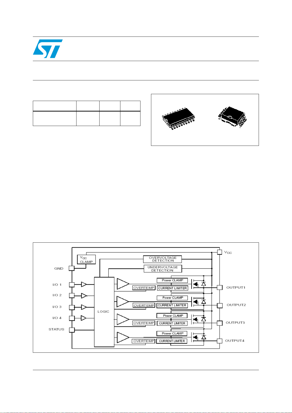
Figure 1. Block diagram
(1)
DS(on)
I
out
270 mΩ 0.25 A 36 V
VNQ860-E
VNQ860SP-E
Quad channel high side driver
V
CC
SO 20 PowerSO-10
Description
The VNQ860-E, VNQ860SP-E are monolithic
devices made using STMicroelectronics VIPower
M0-3 technology, intended for driving any kind of
load with one side connected to ground. Active
current limitation combined with thermal
shutdown and automatic restart protect the device
against overload. Device automatically turns OFF
in case of ground pin disconnection. This device
is especially suitable for industrial applications in
norms conformity with IEC 61131,
(Programmable controllers international
standard).
TM
September 2010 Doc ID 10964 Rev 6 1/19
www.st.com
19

Contents VNQ860-E, VNQ860SP-E
Contents
1 Maximum rating . . . . . . . . . . . . . . . . . . . . . . . . . . . . . . . . . . . . . . . . . . . . . 3
2 Pin connection . . . . . . . . . . . . . . . . . . . . . . . . . . . . . . . . . . . . . . . . . . . . . . 4
3 Electrical characteristics . . . . . . . . . . . . . . . . . . . . . . . . . . . . . . . . . . . . . 5
4 Truth table and switching characteristics . . . . . . . . . . . . . . . . . . . . . . . . 7
5 Typical application schematic . . . . . . . . . . . . . . . . . . . . . . . . . . . . . . . . . 8
6 Waveforms . . . . . . . . . . . . . . . . . . . . . . . . . . . . . . . . . . . . . . . . . . . . . . . . . 9
7 PowerSO-10™ thermal data . . . . . . . . . . . . . . . . . . . . . . . . . . . . . . . . . . 10
8 Reverse polarity protection . . . . . . . . . . . . . . . . . . . . . . . . . . . . . . . . . . 11
9 Package mechanical data . . . . . . . . . . . . . . . . . . . . . . . . . . . . . . . . . . . . 12
10 Order codes . . . . . . . . . . . . . . . . . . . . . . . . . . . . . . . . . . . . . . . . . . . . . . . 17
11 Revision history . . . . . . . . . . . . . . . . . . . . . . . . . . . . . . . . . . . . . . . . . . . 18
2/19 Doc ID 10964 Rev 6
VNQ860-E, VNQ860SP-E Maximum rating
1 Maximum rating
Table 1. Absolute maximum rating
Val ue
Symbol Parameter
SO20 PowerSO-10
Unit
V
-V
-I
I
OUT
-I
V
I
STAT
V
P
T
DC supply voltage 41 V
CC
Reverse DC supply voltage -0.3 V
CC
DC reverse ground pin -200 mA
GND
DC output current Internally limited A
Reverse DC output current -2 A
OUT
DC input current ± 10 mA
I
IN
Input voltage range -3/+V
IN
DC status voltage + V
Electrostatic discharge (R = 1.5 kΩ; C = 100 pF) 2000 V
ESD
Power dissipation at Tc <= 25 °C 16 90 W
tot
Junction operating temperature Internally limited ° C
T
J
T
Case operating temperature -40 to 150 ° C
c
Storage temperature -55 to 150 °C
stg
Table 2. Thermal data
Symbol Parameter
CC
CC
Val ues
SO20 PowerSO-10
V
V
Unit
R
R
R
Thermal resistance junction-pins Max 8 - °C/W
thJP
52
Thermal resistance junction-ambient Max 58
thJA
Thermal resistance junction-case Max - 1.4 °C/W
thJC
37
(1)
(2)
°C/W
1. When mounted on FR4 printed circuit board with 0.5 cm2 of copper area (at least 35µ thick) connected to
all V
pins.
CC
2. When mounted on FR4 printed circuit board with 6 cm2 of copper area (at least 35µ thick) connected to all
pins.
V
CC
Doc ID 10964 Rev 6 3/19
Pin connection VNQ860-E, VNQ860SP-E
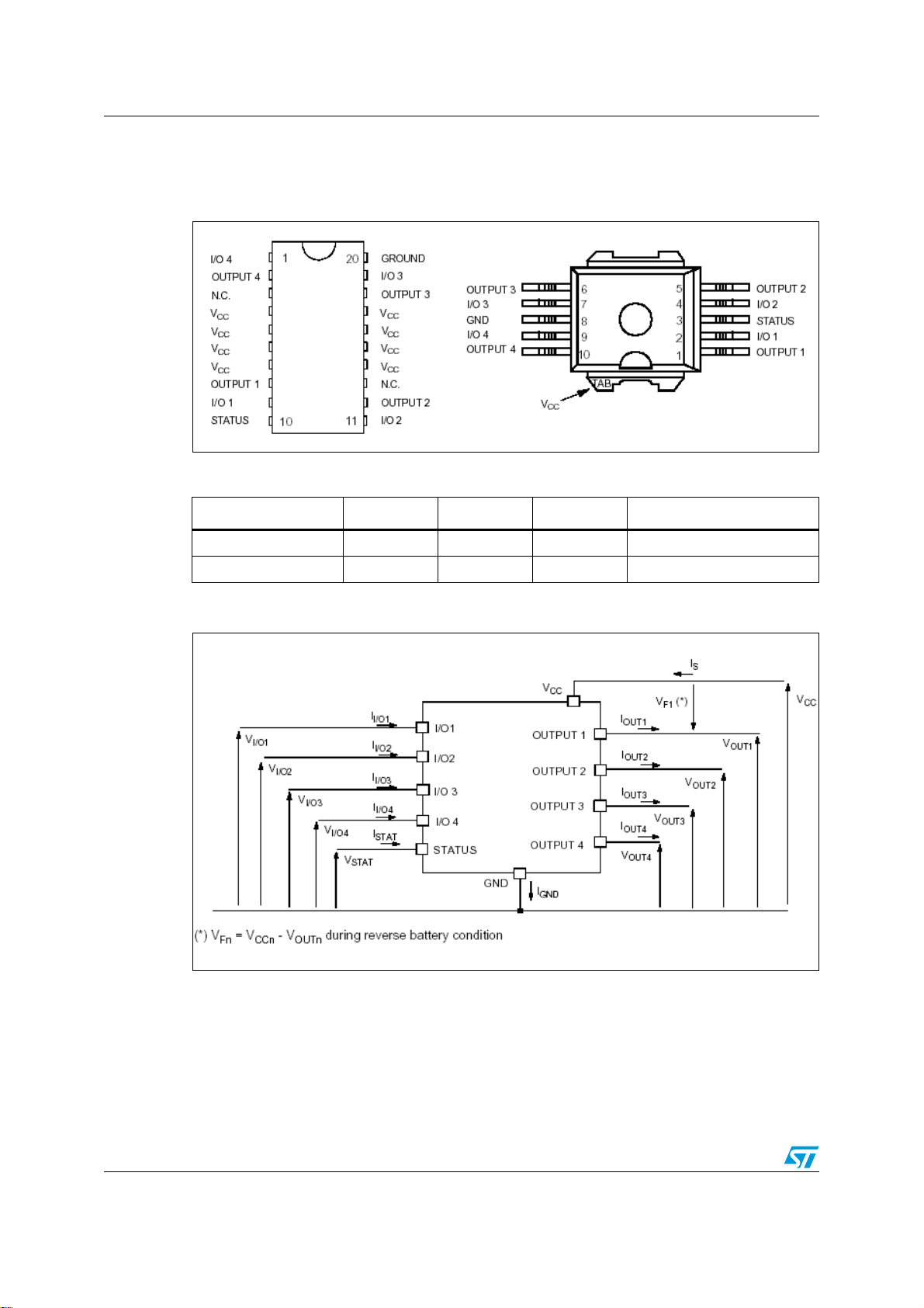
2 Pin connection
Figure 2. Configuration diagram (top view)
Table 3. Pin connection
Connection / pin Status N.C. Output Input
Floating X X X X
To ground X Through 10 kΩ resistor
Figure 3. Current and voltage conventions
4/19 Doc ID 10964 Rev 6
VNQ860-E, VNQ860SP-E Electrical characteristics
3 Electrical characteristics
8 V < VCC < 36 V; -40 °C < T
< 150 °C; unless otherwise specified.
J
Table 4. Power section
Symbol Parameter Test conditions Min. Typ. Max. Unit
V
CC
V
USD
V
OV
R
ON
I
S
I
LGND
I
L(OFF)
I
OUTleak
I
OUTleak
Operating supply
voltage
5.5 36 V
Undervoltage shutdown 3 4 5.5 V
Overvoltage shutdown 36 42 48 V
On state resistance
(per channel)
Supply current
I
= 0.25 A; TJ = 25 °C;
OUT
= 0.25 A;
I
OUT
OFF state; V
CC
TC = 25 °C
= 24 V;
270
540
70512010µA
ON state (all channels ON)
- V
= V
=
IN
1mA
= 0 V 0 10 µA
= 0 V;
= 24 V; TA = 25 °C
= 0 V; V
CC
= 24 V;
240 µA
100 µA
Output current
OFF state output
current
OFF state output
leakage current
OFF state output
leakage current
V
CC
STAT
V
= 24 V;
GND
= 0 V
V
OUT
V
= V
IN
OUT
V
= V
IN
GND
V
= V
CC
OUT
= V
V
IN
GND
= 10 V; TA = 25 °C
V
OUT
mΩ
mA
Table 5. Switching (VCC = 24 V)
Symbol Parameter Test conditions Min. Typ. Max. Unit
t
(ON)
t
(OFF)
(dV
OUT
(dV
OUT
Turn-on delay time of
Output current
Turn-off delay time of
Output current
/dt)onTurn-on voltage slope
/dt)
Turn-off voltage slope
off
RL = 96 Ω from V
to
VOUT
= 2.4 V
RL = 96 Ω from V
to
R
= 21.6 V
VOUT
= 96 Ω from V
L
19.2 V
R
= 96 Ω from V
L
2.4 V
rising edge
IN
rising edge
IN
= 2.4 V to
OUT
= 21.6 V to
OUT
-10-µs
-40-µs
-0.75-V/µs
-0.25-V/µs
Doc ID 10964 Rev 6 5/19
Electrical characteristics VNQ860-E, VNQ860SP-E
Table 6. Protections (per channel)
Symbol Parameter Test conditions Min. Typ. Max. Unit
T
T
V
demag
I
lim
(hyst)
TSD
T
Current limitation 0.35 0.7 1.1 A
Thermal hysteresis 7 15 °C
Thermal shutdown
temperature
Reset temperature 135 °C
R
Turn-off output clamp
voltage
= 0.25 A, VCC = 24 V
I
OUT
150 175 200 °C
V
-59VCC-52VCC-
CC
47
Table 7. Logical input (per channel)
Symbol Parameter Test conditions Min. Typ. Max. Unit
V
V
I
V
I(HYST)
I
V
I
IL
IH
IN
OL
Low level input voltage - 1.25 V
IL
Low level input current V
High level input
IH
voltage
High level input
current
Input hysteresis
voltage
Input current V
I/O output voltage I
= 1.25 V 1 - µA
IN
3.25 - V
= 3.25 V - 10 µA
V
IN
0.5 - V
= V
IN
= 5 mA (fault condition) - 1 V
IN
= 36 V - 200 µA
CC
V
Table 8. Status pin
Symbol Parameter Test conditions Min. Typ. Max. Unit
V
STAT
I
LSTAT
C
STAT
Status low output
voltage
Status leakage
current
Status pin input
capacitance
I
STAT
Normal operation;
V
STAT
Normal operation;
V
STAT
Table 9. VCC - output diode
6/19 Doc ID 10964 Rev 6
Symbol Parameter Test conditions Min. Typ. Max. Unit
V
F
Forward on voltage -I
OUT
= 5 mA (fault condition) - - 1 V
= VCC = 36 V
= 5 V
--10µA
--100pF
= 0.3 A; TJ = 150 °C - - 1 V
 Loading...