


®
VND830ASP
DOUBLE CHANNEL HIGH SIDE SOLID STATE RELAY
TYPE R
DS(on)
I
OUT
V
CC
VND830ASP 60 mΩ (*) 6 A (*) 36 V (*)
(*) Per channel
■ DC SHORT CIRCUIT CURRENT: 6A
■ CMOS COMPATIBLE INPUTS
■ PROPORTIONAL LOAD CURRENT SENSE
■ UNDERVOLTAGE AND OVERVOLTAGE
SHUT-DOWN
■ OVERVOLTAGE CLAMP
■ THERMAL SHUT-DOWN
■ CURRENT LIMITATION
■ VERY LOW STAND-BY POWER DISSIPATION
■ PROTECTI ON AGAINST:
LOSS OF GROUND AND LOSS OF V
■ REVERSE BATTERY PROTECTION (**)
CC
DESCRIPTION
The VND830ASP is a monolithic device made using
STMicroelect ronics VIPower M0-3 technology. It
is intende d for driving any kind o f load with one
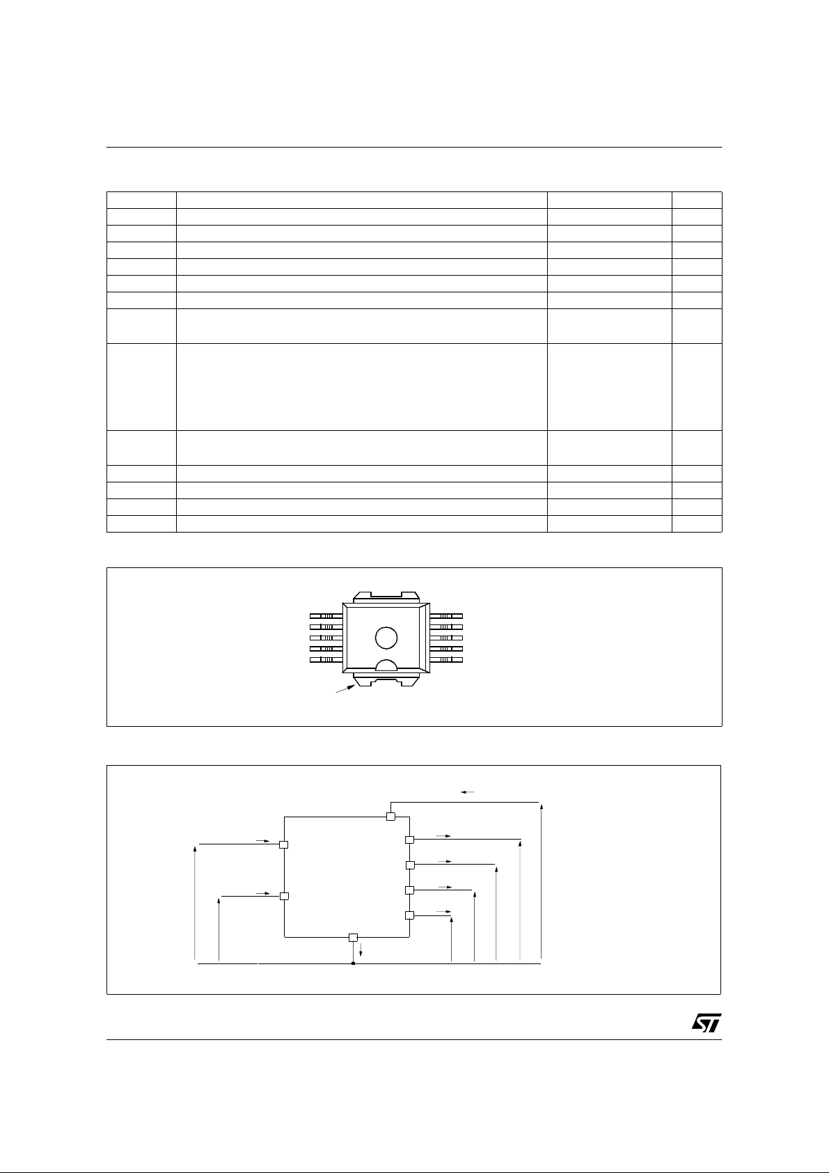
BLO C K DIAG RA M
10
1
PowerSO-10
™
ORDER CODES
PACKAGE TUBE T&R
VND830ASP VND830ASP13TR
PowerSO-10
™
side connected to ground. A cti ve VCC pin voltage
clamp protects the device against low energy
spikes (see ISO7637 transient compatibility table).
This device has two channels in high side
configuration; each channel has an ana log sense
output on which the sensing current is proportional
(according to a known rati o ) to the corr esponding
load current. Built-in thermal shut-down and
outputs current limitation protect the chip from
over temperature and short circuit. Device turns off
in case of ground pin disconnection.
V
CC
OVERVOLTAGE
V
CLAMP
CC
INPUT 1
INPUT 2
GND
OVERTEMP. 1
OVERTEMP. 2
(**) See application schematic at page 8
LOGIC
Ot1
Ot2
UNDERVOLTAGE
DRIVER 1
I
OUT1
DRIVER 2
I
OUT2
PwCLAMP 1
I
LIM1
V
dslim1
K
PwCLAMP 2
I
LIM2
V
dslim2
K
OUTPUT 1
Ot1
CURRENT
SENSE 1
OUTPUT 2
Ot2
CURRENT
SENSE 2
November 2003 1/17
VND830ASP
ABSOLUTE MAXIMUM RATI NG
Symbol Parameter Value Unit
V
-V
-I
GND
I
OUT
I
V
CSENSE
V
E
MAX
P
T
CC
I
R
IN
ESD
tot
T
T
stg
DC Supply Voltag e 41 V
Reverse Supply Voltage - 0.3 V
CC
DC Reverse Ground Pin Current - 200 mA
Output Current Internally Limited A
Reverse Output Current - 6 A
Inpu t C urrent +/- 10 mA
Current Sense Maximum Volta ge
-3
+15
Electro static Discharge (H um an Body Mo del: R=1.5Ω ; C=100pF)
- INPU T
- CURRENT SENSE
- OUTPU T
- V
CC
Maximum Switching Energy
(L=1.8mH; R
=0Ω; V
L
=13.5V; T
bat
=150ºC; IL=9A)
jstart
4000
2000
5000
5000
100 mJ
Power Dissipation at TC=25°C 74 W
Junction Operating Temperature Internally Limited °C
j
Case Operating Temperature - 40 to 150 °C
c
Storage Temperature - 55 to 150 °C
V
V
V
V
V
V
CONNECTION DIAGRAM (TOP VIEW)
GROUND
INPUT2
INPUT1
C.SENSE1
C.SENSE2
6
7
8
9
10
11
V
CC
CURRENT AND VOLTAGE CONVENTIONS
I
IN1
V
IN1
I
IN2
V
IN2
INPUT1
CURRENT SENSE 1
INPUT2
CURRENT SENSE 2
GROUND
V
CC
OUTPUT1
OUTPUT2
I
GND
5
4
3
2
1
V
I
OUT1
I
SENSE1
I
OUT2
I
SENSE2
SENSE2
V
V
OUT2
OUTPUT 2
OUTPUT 2
N.C.
OUTPUT 1
OUTPUT 1
I
S
SENSE1
V
OUT1
V
CC
2/17
VND830ASP
THERMAL DATA
Symbol Parameter Value Unit
R
thj-case
R
thj-amb
(*) When mounted on a standard single-sided FR-4 board with 0.5cm2 of Cu (at least 35µm thick). Horizontal mounting and no artificial air
flow
ELECTRICAL CHARACTERISTICS (8V<VCC<36V; -40°C< Tj <150°C, unless otherwise specified)
(Per each channel)
POWER OUTPUT
Symbol Parameter Test Conditions Min Typ Max Unit
V
CC
V
USD
V
OV
R
ON
V
clamp
I
I
L(off1)
I
L(off2)
I
L(off3)
I
L(off4)
Thermal R esistanc e Junction-case 1.2 °C/W
Thermal Resistanc e Junctio n-ambient 51.2 (*) °C/W
Operating Supply Voltage 5.5 13 36 V
Undervolt age Shut- down 3 4 5.5 V
Overvolt age Shut-down 36 V
=2A; Tj=25°C
I
On State Resistance
OUT
I
=2A; Tj=150°C
OUT
Clamp voltage ICC=20 mA (see note 1) 41 48 55 V
Supply Current
S
Off State Output Current VIN=V
Off State Output Current VIN=0V; V
Off State Output Current VIN=V
Off State Output Current VIN=V
Off State; V
Off State; V
T
=25°C
j
On State; V
R
SENSE
OUT
OUT
OUT
=13V; V
CC
=13V; V
CC
IN=VOUT
IN=VOUT
=0V
=0V;
12
12
=5V; VCC=13V; I
IN
OUT
=0A;
=3.9KΩ
=0V; VCC=36V; Tj=125°C 0 50 µA
=3.5V -75 0 µA
OUT
=0V; VCC=13V; Tj =125°C 5 µA
=0V; VCC=13V; Tj =25°C 3 µA
60
120
40
25
7
mΩ
mΩ
µA
µA
mA
SWITCHING (VCC =13V)
Symbol Parameter Test Conditions Min Typ Max Unit
R
=6.5Ω from VIN rising edge to
t
d(on)
t
d(off)
Turn-on Delay Time
Turn-off Delay Ti me
L
=1.3V
V
OUT
RL=6.5Ω from VIN falling edge to
V
=11.7V
OUT
30 µs
30 µs
See
/dt
dV
OUT
Turn-on Voltage Slope RL=6.5Ω from V
(on)
=1.3V to V
OUT
OUT
=10.4V
relative
diagram
See
/dt
dV
OUT
Turn-off Volta g e Slope RL=6.5Ω from V
(off)
=11.7V to V
OUT
OUT
=1.3V
relative
diagra m
LOGIC INPUT (Channels 1,2)
Symbol Parameter Test Conditions Min Typ Max Unit
V
I
V
I
V
I(hyst)
V
Note 1: V
Input low level voltage 1.25 V
IL
Low level input current VIN=1.25V 1 µA
IL
Input high level voltage 3.25 V
IH
High level input current VIN=3.25V 10 µA
IH
Input hy steresi s vo l ta ge 0. 5 V
I
Input clamp voltage
ICL
and VOV are correlated. Typical difference is 5V.
clamp
IN
I
IN
=1mA
=-1mA
66.8
-0.7
8V
V/µs
V/µs
V
3/17
1

VND830ASP
ELECTRICAL CHARACTERISTICS (continued)
VCC - OUTPUT DIODE
Symbol Parameter Test Conditions Min Typ Max Unit
V
F
Forward on Voltage -I
PROTECTIONS
Symbol Parameter Test Conditions Min T yp Max Unit
I
Current limit ati on
lim
T
T
V
demag
V
HYST
Thermal shut-down
TSD
temper ature
Thermal reset temperature 135 °C
T
R
Thermal hystere sis 7 1 5 °C
Turn-of f ou tp ut vo lt age clam p I
Output voltage drop limitation I
ON
=2A; Tj=150°C 0.6 V
OUT
Vcc=13 V
691515A
5.5V<Vcc<36V
150 175 2 00 °C
=2A; VIN=0V; L=6m H VCC-41 VCC-48 VCC-55 V
OUT
=10mA 50 mV
OUT
A
CURRENT SENSE (9V≤V
≤16V) (See figure 1)
CC
Symbol Parameter Test Conditions Min Typ Max Unit
K
K
dK
K
dK
K
dK
I
SENSE
V
SENSE
V
SENSEH
I
0
OUT/ISENSE
I
1
OUT/ISENSE
Current Sense Ratio Drift
1/K1
I
2
OUT/ISENSE
Current Sense Ratio Drift
2/K2
I
3
OUT/ISENSE
Current Sense Ratio Drift
3/K3
Analog Sense Leakage Current
Max Analog Sense Output
Voltage
Sense Vo lt age in
Overtem perature conditions
OUT1
OUT2
=0.05A; V
other channels open; T
I
or I
OUT1
OUT2
=0.25A; V
other channels open; Tj= -40°C...150°C
I
or I
or I
or I
or I
OUT2
OUT2
OUT2
OUT2
=0.25A; V
=1.6A; V
=-40°C
j
=1.6A; V
=2.5A; V
OUT1
other channels open; Tj= -40°C...150°C
I
OUT1
channels open; T
T
=25°C...150°C
j
I
OUT1
channels open; Tj=-40°C...150°C
I
OUT1
channels open; Tj=-40°C
T
=25°C...150°C
j
I
or I
OUT1
channels open; Tj=-40°C...150°C
V
=0V; I
IN
T
=-40°C...150°C
j
V
=5V; I
IN
T
=-40°C...150°C
j
=5.5V ; I
V
CC
V
>8V, I
CC
=13V; R
V
CC
OUT2
OUT
OUT
OUT1,2
OUT1,2
SENSE
=2.5A; V
=0A; V
=0A; V
=1.3A; R
=2.5A; R
=3.9kΩ
SENSE
SENSE
=0.5V;
SENSE
= -40°C...150°C
j
=0.5V;
SENSE
=0.5V;
SENSE
=4V; ot he r
SENSE
=4V; ot he r
SENSE
=4V; ot he r
SENSE
=4V; ot he r
SENSE
=0V;
=0V;
=10kΩ
SENSE
=10kΩ
SENSE
600 1300 2000
1000 1400 1900
-10 +10 %
1280
1300
1500
1500
1800
1780
-6 +6 %
1280
1340
1500
1500
1680
1600
-6 +6 %
0
0
5
10
2
4
5.5 V
I
or I
Analog Sense Output
R
VSENSEH
Impeda nce in
VCC=13V; Tj>T
; All Channels Open 400 Ω
TSD
Overtemperatur e Condition
t
DSENSE
Curre nt sense dela y
response
to 90% I
(see note 2) 500 µs
SENSE
µA
µA
V
V
Note 2: current sense signal delay after positive input sl ope.
Note: Sense pin doesn’t have to be left floating.
4/17

TRUTH TABLE (per channel)
CONDITIONS INPUT OUTPUT SENSE
Normal op eration
Overtemperature
Undervoltage
Overvoltage
L
H
L
H
L
H
L
H
L
Short circuit to GND
H
H
Short circuit to V
CC
Negative output voltage
clamp
L
H
LL 0
ELECTRICAL TRANS IENT REQUIREMENTS
VND830ASP
L
H
L
L
L
L
L
L
L
L
L
(T
j<TTSD
(T
j>TTSD
H
H
0
Nominal
0
V
SENSEH
0
0
0
0
0
) 0
) V
SENSEH
0
< Nomin a l
ISO T/R 7637/1
Test Pulse
I II III IV Delays and
TEST LEVELS
Impedance
1 -25 V -50 V -75 V -100 V 2 m s 10 Ω
2 +25 V +50 V +75 V +100 V 0.2 ms 10 Ω
3a -2 5 V -50 V -100 V -150 V 0.1 µs 50 Ω
3b +25 V +50 V +75 V +100 V 0.1 µs 50 Ω
4 -4 V -5 V -6 V -7 V 100 ms, 0.01
5 +26.5 V +46.5 V +66.5 V +86.5 V 400 ms, 2
ISO T/R 7637/1
Test Pulse
I II III IV
TEST LEVE LS RESULTS
Ω
1CCCC
2CCCC
3aCCCC
3bCCCC
4CCCC
5C E E E
CLASS CONTENTS
C All funct ions of t he device are performed as designed aft er exposure to disturbance.
E
One or more functions of the device is not performed as designed after exposure to disturbance
and cann ot be returned to proper opera tion without repl acing the d evice.
Ω
5/17

VND830ASP
Figur e 1: I
OUT/ISENSE
versus I
OUT
Iout/Isense
2250
2000
1750
max Tj=25...150ºC
1500
min Tj=25...150ºC
1250
1000
750
500
0 0.5 1 1.5 2 2.5 3
Iout (A)
Figur e 2: Switching Characteristics (Resistive load RL=6.5Ω)
max Tj= -40ºC
typical value
min Tj= -40ºC
V
OUT
dV
OUT
I
SENSE
INPUT
/dt
(on)
t
d(on)
80%
90%
t
DSENSE
90%
dV
/dt
OUT
(off)
t
r
10%
t
f
t
t
t
d(off)
t
6/17

Figure 3: Waveforms
INPUT
n
LOAD CURREN T
SENSE
n
V
CC
INPUT
n
LOAD CURRENT
SENSE
n
V
CC
INPUT
n
LOAD CURRENT
SENSE
n
VND830ASP
NORMAL OPERATION
n
UNDERVOLTAGE
V
USDhyst
V
USD
n
OVERVOLTAG E
V
OV
VCC < V
OV
n
VCC > V
OV
INPUT
n
LOAD CURRENT
LOAD VOLTAGE
SENSE
n
INPUT
n
LOAD VOLTAGE
LOAD CURREN T
SENSE
n
T
j
INPUT
n
LOAD CURRENT
SENSE
n
SHORT TO GROUND
n
n
SHORT TO V
n
n
<Nominal
T
TSD
T
R
n
OVERTEMPERATURE
CC
<Nominal
I
SENSE
=
V
SENSEH
R
SENSE
7/17

VND830ASP
APPLICATION SCHEMATIC
+5V
R
prot
R
µ
C
prot
R
prot
INPUT1
CURRENT SENSE1
INPUT2
V
CC
D
ld
OUTPUT1
R
SENSE1
R
prot
CURRENT SENSE2
R
SENSE2
GND PROTECTION NETWORK AGAINST
REVERSE BATTERY
Soluti on 1: Resistor in the ground line (R
can be us ed with any t ype of load.
The fo llowin g is an indica tion on how to dim ension the
resistor.
R
GND
1) R
2) R
where -I
be found in the absolute maximum rating section of the
≤ 600mV / I
GND
≥ (−VCC) / (-I
GND
is the DC re vers e grou nd pi n cu rren t an d can
GND
S(on)max
)
GND
.
device’s datasheet.
Power Dissipation in R
battery situations) is:
= (-VCC)2/R
P
D
GND
(when VCC<0: during reverse
GND
This resistor can be shared amongst several different
HSD. Please note that the value of this resistor should be
calcul ated with form ula (1) wher e I
sum of the maximum on-state currents of the different
S(on)max
devices.
Please note that if the microprocessor ground is not
common with the device ground then the R
produce a shift (I
and the status output values. This shift will vary
S(on)max
* R
) in the input thresholds
GND
depend ing on how many devi ces are ON in the c ase of
several high side drivers sharing t he same R
only). This
GND
becomes t he
GND
.
GND
will
GND
R
V
GND
GND
D
OUTPUT2
GND
If the calculated power dissipation leads to a large resistor
or seve ral de vic es have to s hare t he s ame r esisto r then
the ST suggests to utilize Solu tion 2 (see below).
Solution 2:
A resistor (R
D
GND
A diode (D
=1kΩ) should be inserted in parallel to
GND
if the devi ce will be driving a n inductive load.
) in the gro und line.
GND
This small signal diode can be safely shared amongst
several different HSDs. Also in this case, the presence of
j
the ground network wi ll produce a shift (
600mV) in t he
input thresholds and the status output values if the
microprocessor ground is not common with the device
ground. This shift will not vary if more than one HSD
shares the same diode/resistor net w ork.
Series resistor in INPUT line is also required to prevent
that, dur ing battery voltage transient, the current exceeds
the Absolute Maximum Rating.
Safest c onfigura tion for unused INPUT pin is to l eave it
unconnected, while unused SENSE pin has to be
connected to Ground pin.
LOAD DUMP PROTECTION
Dld is necessary (Voltage Transient Suppressor) if the
load dump peak voltage exceeds VCC max DC rating. The
same applies if the device will be subject to transients on
the VCC line that are grea ter tha n the ones sh own in the
ISO T/R 7637/1 table.
8/17

C I/Os PROTECTION:
µ
If a ground protection network is used and negative
transient are present on the VCC line, the control pins will
be pulled negative. ST suggests to insert a resistor (R
in line to prevent the µC I/Os pins to latc h-up.
prot
The v alu e of these res i s t or s is a c om promise be t w ee n the
leakage current of µC and the current required by the
HSD I/Os (Input levels compatibility) with the latch-up limit
of µC I/Os.
-V
CCpeak/Ilatchup
Calculation example:
)
For V
CCpeak
5kΩ ≤ R
Recommended R
= - 100V an d I
≤ 65kΩ.
prot
≤ R
≤ (V
prot
value is 10kΩ.
prot
OHµC-VIH-VGND
≥ 20mA; V
latchup
VND830ASP
) / I
IHmax
≥ 4.5V
OHµC
9/17

VND830ASP
Off State Output Current
IL(off1) (uA)
8
7
6
5
4
3
2
1
0
-50 -25 0 25 50 75 100 125 150 175
Off stat e
Vcc=13V
Vin=Vout=0V
Tc (ºC)
Input Clamp Voltage
Vicl (V)
8
7.8
7.6
7.4
7.2
7
6.8
6.6
6.4
6.2
6
Iin=1mA
-50 -25 0 25 50 75 100 125 150 175
Tc (ºC)
High Level Input Current
Iih (uA)
5
4.5
3.5
2.5
1.5
Vin=3.25V
4
3
2
1
-50 -25 0 25 50 75 100 125 150 175
Input High Level
Vih (V)
3.6
3.4
3.2
3
2.8
2.6
2.4
2.2
2
Vcc=13V
-50 -25 0 25 50 75 100 125 150 175
Input Hysteresis VoltageInput Low Level
Tc (ºC)
Tc (ºC)
Vil (V)
2.6
2.4
2.2
2
1.8
1.6
1.4
1.2
1
Vcc=13V
-50 -25 0 25 50 75 100 125 150 175
Tc (ºC)
10/17
Vhyst (V)
1.5
1.4
1.3
1.2
1.1
1
0.9
0.8
0.7
0.6
0.5
Vcc=13V
-50 -25 0 25 50 75 100 125 150 175
Tc (ºC)

Overvoltage Shutdown
I
LIM
Vs T
VND830ASP
case
Vov (V)
50
47.5
45
42.5
40
37.5
35
32.5
30
-50 -25 0 25 50 75 100 125 150 175
Ilim (A)
20
17.5
15
12.5
10
7.5
2.5
Vcc=13V
5
0
-50 -25 0 25 50 75 100 125 150 175
Tc (ºC)
Turn-on Voltage Slope Turn-off Voltage Slope
dVout/dt(on) (V/ms)
600
550
500
450
400
350
300
250
200
Vcc=13V
Rl=6.5Ohm
-50 -25 0 25 50 75 100 125 150 175
Tc (ºC)
dVout/dt(off) (V/ms)
500
450
400
350
300
250
200
150
100
50
Vcc=13V
Rl=6.5Ohm
0
-50 -25 0 25 50 75 100 125 150 175
Tc (ºC)
Tc (ºC)
On State Resistance Vs T
case
Ron (mOhm)
100
90
80
70
60
50
40
30
20
10
0
-50 -25 0 25 50 75 100 125 150 175
Iout=5A
Vcc=8V & 36V
Tc (ºC)
On State Resistance Vs V
CC
Ron (mOhm)
100
90
80
70
60
50
40
30
20
Iout=5A
5 10152025303540
Tc=150ºC
Tc=25ºC
Tc= -40ºC
Vcc (V)
11/17

VND830ASP
Maximum turn off current versus load inductance
LMAX (A)
I
100
10
A
B
C
1
0.1 1 10 100
A = Single Pulse at T
B= Repetitive pulse at T
C= Repetitive Pulse at T
Conditions:
VCC=13.5V
Values are generated with RL=0Ω
In case of repetitive pulses, T
the temperature specified above for curves B and C.
VIN, I
L
=150ºC
Jstart
=100ºC
Jstart
=125ºC
Jstart
jstart
Demagnetization
(at beginning of each demagnetization) of every pulse must not exceed
L(mH)
Demagnetization
Demagnetization
12/17
t

PowerSO-10™ PC Board
VND830ASP
PowerSO-10™ THERMAL DATA
R
thj-amb
Layout condition of Rth and Zth measurements (PCB FR 4 area= 58mm x 58mm, PCB thickness =2mm,
Cu thickness=35µm, Copper areas: from minimum pad lay-out to 8cm
Vs PCB copper area in open box free air condition
2
).
RTHj_amb (°C/W)
55
Tj-Tamb=50°C
50
45
40
35
30
0246810
PCB Cu heatsink area (cm^2)
13/17

VND830ASP
PowerSO-10 Thermal Impedance Junction Ambient Single Pulse
ZTH (°C/W)
1000
100
10
1
0.1
0.0001 0.001 0.01 0.1 1 10 100 1000
Time (s)
Thermal fitting model of a double channe l HSD
in PowerSO-10
Pulse calculation formula
Z
THδ
where
RTHδ Z
δ tpT⁄=
THtp
2
0.5 cm
2
6 cm
1 δ–()+⋅=
Tj_1
Tj_2
14/17
Pd1
C1
C1 C2
R1
Pd2
Thermal Parameter
C3 C4
R3R1 R6R5R2
R2
T_amb
C5 C6C2
R4
Area/island (cm2)0.56
R1 (°C/W) 0.15
R2 (°C/W) 0.8
R3( °C/W) 0.7
R4 (°C/W) 0.8
R5 (°C/W) 12
R6 (°C/W) 37 22
C1 (W.s/°C) 0.0006
C2 (W.s/°C) 2.10E-03
C3 (W.s/°C) 0.013
C4 (W.s/°C) 0.3
C5 (W.s/°C) 0.75
C6 (W.s/°C) 3 5

PowerSO-10™ MECHANICAL DATA
VND830ASP
DIM.
MIN. TYP MAX. MIN. TYP. MAX.
mm. inch
A 3.35 3.65 0.132 0.144
A (*) 3.4 3.6 0.134 0.142
A1 0.00 0.10 0.000 0.004
B 0.40 0.60 0.016 0.024
B (*) 0.37 0.53 0.014 0.021
C 0.35 0 .55 0.013 0.022
C (*) 0.23 0.32 0.009 0.0126
D 9.40 9 .60 0.370 0.378
D1 7.40 7.60 0.291 0.300
E 9.30 9.50 0.366 0.374
E2 7.20 7.60 0.283 300
E2 (*) 7.30 7.50 0.287 0.295
E4 5.90 6.10 0.232 0.240
E4 (*) 5.90 6.30 0.232 0.248
e 1.27 0.050
F 1.25 1.35 0.049 0.053
F (*) 1.20 1 .40 0.047 0.055
H 13.80 14.40 0.543 0.567
H (*) 13.85 14.35 0.545 0.565
h 0.50 0.002
L 1.20 1.80 0.047 0.070
L (*) 0.80 1.10 0.031 0.043
α 0º 8º 0º 8º
α (*) 2º 8º 2º 8º
(*) Muar only POA P013P
HE
h
A
F
A1
10
1
eB
0.25
D
= =
D1
= =
E2
DETAIL "A"
DETA IL "A"
B
0.10 A
SEATING
PLANE
A
C
α
B
E4
SEATING
PLANE
A1
L
P095A
15/17

VND830ASP
PowerSO-10™ SUGGESTED PAD LAYOUT
14.6 - 14.9
10.8 - 11
6.30
0.67 - 0.73
1
2
3
9.5
4
5
10
0.54 - 0.6
9
8
7
1.27
6
TAPE AND REEL SHIPMENT (suffix “13TR”)
TUBE SHIPMENT (no suffix)
C
A
B
A
All dimensi ons ar e in mm.
Base Q.ty Bulk Q.ty Tube length (± 0. 5) A B C (± 0.1)
Casablanca 50 10 00 532 10.4 16.4 0.8
Muar 50 1000 532 4.9 17.2 0.8
MUARCASABLANCA
B
REEL DIMENSIONS
Base Q.ty 600
Bulk Q.ty 600
A (max) 330
B (min) 1.5
C (± 0.2) 13
F 20.2
G (+ 2 / -0) 24.4
N (min) 60
T (max) 30.4
C
TAPE DIMENSIONS
According to Electronic Industries Association
(EIA) Standard 481 rev. A, Feb 1986
Tape width W 24
Tape Hole Spacing P0 (± 0.1) 4
Component Spacing P 24
Hole Diameter D (± 0.1/-0) 1.5
Hole Diameter D1 (min) 1.5
Hole Position F (± 0.05) 11.5
Compartm ent Depth K (max) 6.5
Hole Spacing P1 (± 0.1) 2
All dimensions are in mm.
Top
cover
tape
End
500mm min
All dimensions are in mm.
Empty components pockets
saled with cover tape.
User direction of feed
500mm min
Start
No componentsNo components Components
16/17
1

VND830ASP
Information furnished is believed to be accurate and r eliable. Howev er, STMicroelectr onics assume s no r es ponsibility for the consequences
of use of such information nor for any infringement of patents or other rights of third parties which may results from its use. No license is
granted by implication or otherwise under any patent or patent rights of STMi c r oelectronic s . Specifications mentioned in this publication are
subject to c hange withou t notice. This publicatio n s upersedes and replaces all informati on previously s upplied. ST M icroelectr on ics product s
are not authorized for use as critical components in life support devices or systems without express written approval of STMicroelectronics.
Australia - Brazil - Canada - Ch ina - Finland - Franc e - Germany - Hong Kong - India - Isra el - Italy - Japan - M alaysia -
Malta - Morocco - Singapore - Spain - Sweden - Switzerland - United Kingdom - U.S.A.
The ST logo is a trademark of ST M ic r oelectronic s
2003 STMicroelectronics - Printed in ITALY- All Rights Reserved.
STMicroelectronics GROUP OF COMPANIES
http://www.st.com
17/17
 Loading...