

Page 1

VND810MSP-E
1
1
DOUBLE CHANNEL HIGH SIDE DRIVER
Table 1. General Features
Type R
VND810MSP-E 150 mΩ (*) 0.6 A (*) 36 V
(*) Per each channel
CMOS COMPATIBLE INPUTS
■
■ OPEN DRAIN STATUS OUTPUTS
■ ON STATE OPEN LOAD DETECTION
■ OFF STATE OPEN LOAD DETECTION
■ SHORTED LOAD PROTECTION
■ UNDERVOLTAGE AND OVERVOLTAGE
DS(on)
I
out
V
CC
SHUTDOWN
■ PROTECTION AGAINST LOSS OF GROUND
■ VERY LOW STAND-BY CURRENT
■ REVERSE BATTERY PROTECTION (**)
■ IN COMPLIANCE WITH THE 2002/95/EC
EUROPEAN DIRECTIVE
DESCRIPTION
The VND810MSP-E is a monolithic device
designed in STMicroelectronics VIPower M0-3
Technology, intended fo r driving any kind of load
with one side connected to ground.
Active V
pin voltage clamp protects the dev ice
CC
against low energy spikes (see ISO7637 transient
compatibility table).
Figure 1. Package
0
PowerSO-10™
Active current limitation combined with thermal
shutdown and automatic restart protects the
device against overload. The current limitation
threshold is aimed at detecting the 21W/12V
standard bulb as an overload fault. The device
detects open load condition both in on and off
state. Output shorted to V
is detected in the off
CC
state. Device automatically turns off in case of
ground pin disconnection.
Table 2. Order Codes
Package Tube Tape and Reel
PowerSO-10™ VND810MSP-E VND810MSPTR-E
Note: (**) See application schematic at page 9
Rev. 2
1/20March 2005
Page 2
VND810MSP-E
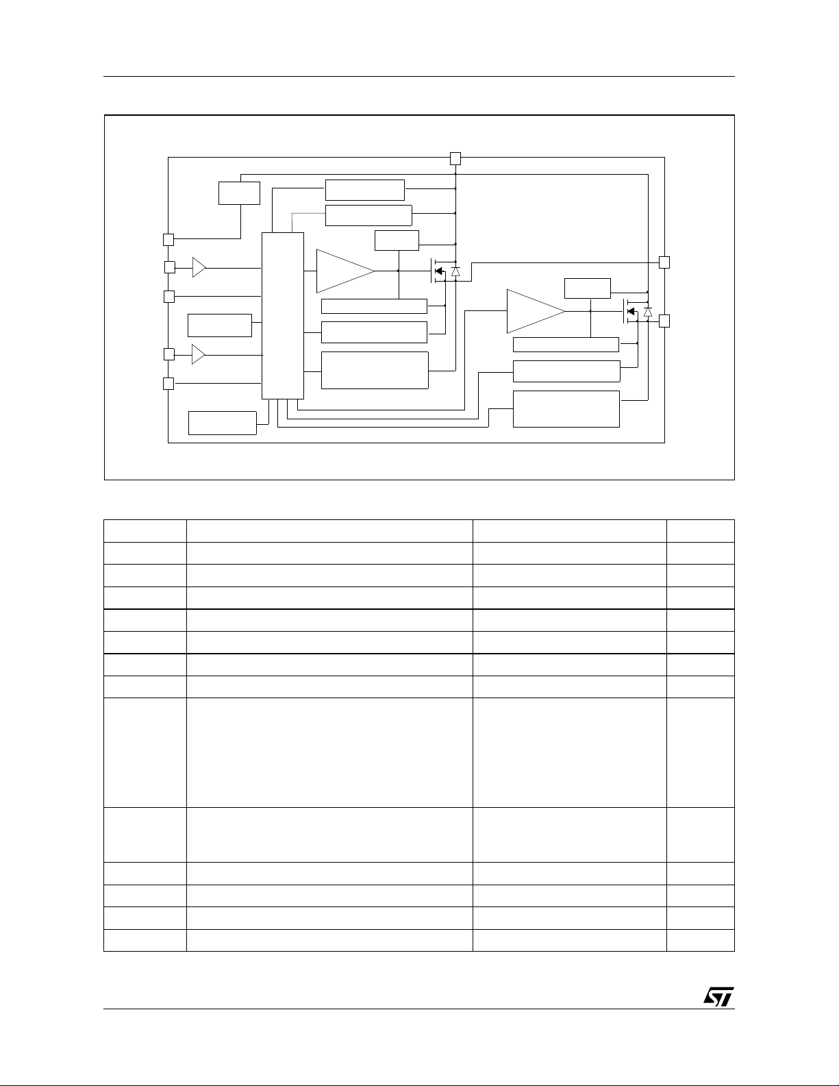
Figure 2. Block Diagram
V
cc
CLAMP
OVERVOLTAGE
UNDERVOLTAGE
GND
INPUT1
STATUS1
INPUT2
STATUS2
OVERTEMP. 1
OVERTEMP. 2
LOGIC
DRIVER 1
CURRENT LIMITER 1
OPENLOAD ON 1
OPENLOAD OFF 1
CLAMP 1
CLAMP 2
DRIVER 2
CURRENT LIMITER 2
OPENLOAD ON 2
OPENLOAD OFF 2
Table 3. Absolute Maximum Ratings
Symbol Parameter Value Unit
DC Supply Voltage 41 V
Reverse DC Supply Vo lta ge - 0.3 V
DC Reverse Ground Pin Current - 200 mA
DC Output Current Internally Limited A
Reverse DC Output Cu rre nt - 6 A
DC Input Current +/- 10 mA
DC Status Current +/- 10 mA
Electrostatic Discharge (Human Body Model:
R=1.5KΩ; C=100pF)
- INPUT
- STATUS
- OUTPUT
- V
CC
4000
4000
5000
5000
Maximum Switching Energy
(L=400mH; R
I
=0.9A)
L
=0Ω; V
L
=13.5V; T
bat
jstart
=150ºC;
225 mJ
Power Dissipation TC=25°C 52 W
Junction Operating Temperature Internally Limited °C
Case Operating Temperature - 40 to 150 °C
Storage Temperature - 55 to 150 °C
- V
- I
- I
V
E
V
CC
GND
I
OUT
OUT
I
IN
I
stat
ESD
MAX
P
T
T
T
stg
CC
tot
j
c
OUTPUT1
OUTPUT2
V
V
V
V
2/20
Page 3

VND810MSP-E
Figure 3. Configuration Diagram (Top View) & Suggested Connections for Unused and N.C. Pins
GROUND
INPUT 1
STA TUS 1
STA TUS 2
INPUT 2
V
CC
Connection / Pin Status N.C. Output Input
Floating X X X X
To Ground X Through 10KΩ resistor
Figure 4. Current and Voltage Conventions
I
IN1
I
V
IN1
V
STAT1
STAT1
I
IN2
I
V
STAT2
IN2
V
STAT2
INPUT 1
STATUS 1
INPUT 2
STATUS 2
6
7
8
9
10
11
5
4
3
2
1
V
CC
OUTPUT 1
OUTPUT 1
N.C.
OUTPUT 2
OUTPUT 2
V
(*)
F1
I
OUT1
I
S
V
CC
OUTPUT 1
V
OUT1
I
OUT2
V
OUT2
GND
OUTPUT 2
I
GND
(*) VFn = V
CCn
- V
during reverse battery condition
OUTn
Table 4. Thermal Data
Symbol Parameter Value Unit
R
thj-case
R
thj-amb
Note: 1. When mounted on a standard single-side d FR-4 board with 0.5 c m2 of Cu (at least 35µm thick). Hori zontal mounti ng and no arti ficial
Note: 2. When mounted on a standard single-sided FR-4 board with 6 cm
Thermal Resistance Junction-case 2.4 °C/W
Thermal Resistance Junction-ambient 52.4
air flow.
air flow.
2
of Cu (at least 3 5µm thick). Horizontal mounting and no artificial
(1)
37
(2)
°C/W
3/20
Page 4
VND810MSP-E
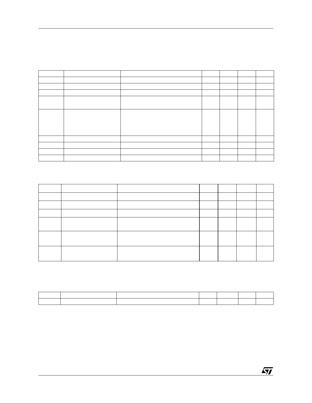
ELECTRICAL CHARACTERISTICS
(8V<V
(Per each channel)
Table 5. Power Outputs
Symbol Parameter Test Conditions Min Typ Max Unit
V
V
V
Note: (**) Per device.
<36V; -40°C<Tj<150°C; unless otherwise specified)
CC
(**) Operating Supply Voltage 5.5 13 36 V
CC
(**) Undervoltage Shut-down 3 4 5.5 V
USD
(**) Over vo ltag e Sh ut- do wn 36 V
OV
R
ON
On State Resistance
IS (**) Supply Current
I
L(off1)
I
L(off2)
I
L(off3)
I
L(off4)
Off State Output Current VIN=V
Off State Output Current VIN=0V; V
Off State Output Current VIN=V
Off State Output Current VIN=V
I
=0.5A; Tj=25°C
OUT
=0.5A; VCC>8V
I
OUT
Off State; V
Off State; V
Tj=25°C
On State; V
OUT
OUT
OUT
=13V; VIN=V
CC
=13V; VIN=V
CC
OUT
OUT
=0V
=0V;
12
12
=13V; VIN=5V; I
CC
OUT
=0A
5
=0V 0 50 µA
=3.5V -75 0 µA
OUT
=0V; VCC=13V; Tj =125°C 5 µA
=0V; VCC=13V; Tj =25°C 3 µA
150
320
40
25
7
mΩ
mΩ
µA
µA
mA
Table 6. Protection (See note 1)
Symbol Parameter Test Conditions Min . Typ. Max. Un it
T
TSD
T
T
hyst
t
SDL
I
lim
V
demag
Note: 1. To ensure long term reliability under heavy overload or short circuit conditions, protection and related diagnostic signals must be
Shut-down Temp era tu re 150 175 200 °C
Reset Temperature 135 °C
R
Thermal Hysteres is 7 15 °C
Status Delay in Overload
Conditions
Current limitation
Turn-off Output Cla mp
Voltage
used together with a proper software strategy. If the dev ice is subjected to abn ormal conditions , this software must limit the duration
and number of activation cycles
Tj>T
TSD
0.6 0.9 1.2
5.5V<V
I
OUT
<36V
CC
=0.5A; L=6mH VCC-41 VCC-48 VCC-55 V
20 µs
1.2
A
A
Table 7. VCC - Output Diode
Symbol Parameter Test Conditions M in T yp Max Unit
V
Forward on Voltage -I
F
=0.5A; Tj=150°C 0.6 V
OUT
4/20
Page 5

VND810MSP-E
ELECTRICAL CHARACTERISTICS (continued)
Table 8. Status Pin
Symbol Parameter Test Conditions M in Typ Max Unit
V
STAT
I
LSTAT
C
STAT
V
SCL
Status Low Output Voltage I
= 1.6 mA 0.5 V
STAT
Status Leakage Current Normal Operation; V
Status Pin Input
Capacitance
Status Clamp Voltag e
Normal Operation; V
I
= 1mA
STAT
= - 1mA
I
STAT
= 5V 10 µA
STAT
= 5V 100 pF
STAT
66.8
-0.7
8V
V
Table 9. Switching (V
CC
=13V)
Symbol Parameter Test Conditions Min Typ Max Unit
R
=13Ω from VIN rising edge to
L
V
=1.3V
OUT
R
=13Ω from VIN falling edge to
L
V
=11.7V
OUT
=13Ω from V
R
L
V
=10.4V
OUT
=13Ω from V
R
L
V
=1.3V
OUT
=1.3V to
OUT
=11.7V to
OUT
30 µs
30 µs
See
relative
diagram
See
relative
diagram
dV
dV
t
d(on)
t
d(off)
OUT
OUT
Turn-on Delay Time
Turn-off Delay Time
/dt
Turn-on Voltage Slope
(on)
/dt
Turn-off Voltage Slope
(off)
Table 10. Openload Detection
Symbol Parameter Test Conditions Min Typ Max Unit
I
OL
t
DOL(on)
V
OL
t
DOL(off)
Openload ON State
Detection Thresho ld
Openload ON State
Detection Delay
Openload OFF State
Voltage Detection
Threshold
Openload Detection Delay
at Turn Off
=5V 20 40 80 mA
V
IN
=0A 200 µs
I
OUT
V
=0V 1.5 2.5 3.5 V
IN
1000 µs
V/µs
V/µs
Table 11. Logic Input
Symbol Parameter Test Conditions Min Typ Max Unit
V
V
V
I
V
I
IH
I(hyst)
ICL
Input Low Level 1.25 V
IL
Low Level Input Current VIN = 1.25V 1 µA
IL
Input High Level 3.25 V
IH
High Level Input Current VIN = 3.25V 10 µA
Input Hysteresis Voltage 0.5 V
Input Clamp Voltage
I
= 1mA
IN
= -1mA
I
IN
66.8
-0.7
8V
V
5/20
Page 6

VND810MSP-E
Figure 5.
OPEN LOAD STATUS TIMING (with external pull-up)
V
> V
OUT
OL
V
INn
V
STAT n
t
DOL(off)
Table 12. Truth Table
CONDITIONS INPUT OUTPUT SENSE
Normal Operation
Current Limitation
Overtemperature
Undervoltage
Overvoltage
Output Voltage > V
Output Current < I
OL
OL
L
H
L
H
H
L
H
L
H
L
H
L
H
L
H
I
OUT
t
DOL(on)
< I
OVER TEMP STATUS TIMING
OL
V
INn
V
STAT n
L
H
L
X
X
L
L
L
L
L
L
H
H
L
H
t
SDL
Tj > T
(T
(T
TSD
< T
j
> T
j
TSD
TSD
t
SDL
) H
) L
H
H
H
H
L
X
X
H
H
L
H
H
L
6/20
Page 7
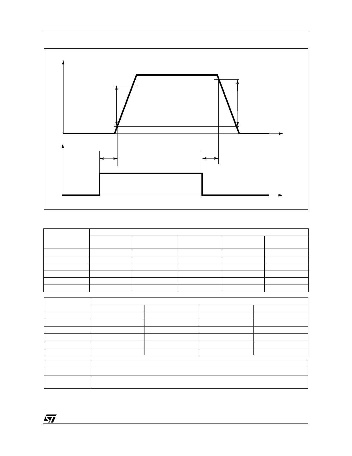
Figure 6. Switching Time Waveforms
V
OUTn
80%
dV
/dt
OUT
(on)
V
INn
t
d(on)
10%
VND810MSP-E
90%
/dt
dV
OUT
(off)
t
td
(off)
t
Table 13. Electrical Transient Requirements On V
CC
ISO T/R 7637/1
Te st Pulse
I II III IV Delays and
1 -25 V -50 V -75 V -100 V 2 ms 10 Ω
2 +25 V + 50 V +75 V +100 V 0.2 ms 10 Ω
3a -25 V -50 V -100 V -150 V 0.1 µs 50 Ω
3b +25 V +50 V +75 V +100 V 0.1 µs 50 Ω
4 -4 V -5 V -6 V -7 V 100 ms, 0.01
5 +26.5 V +46.5 V +66.5 V +86.5 V 400 ms, 2
ISO T/R 7637/1
Te st Pulse
I II III IV
TEST LEVELS RESULTS
1CCCC
2CCCC
3aCCCC
3bCCCC
4CCCC
5CEEE
CLASS CONTENTS
C All functions of the device are performed as designed after exposure to disturbance.
E One or more functions of the device is not performed as designed after exposure and cannot be
returned to proper operation without replacing the device.
Pin
TEST LEVELS
Impedance
Ω
Ω
7/20
Page 8
VND810MSP-E
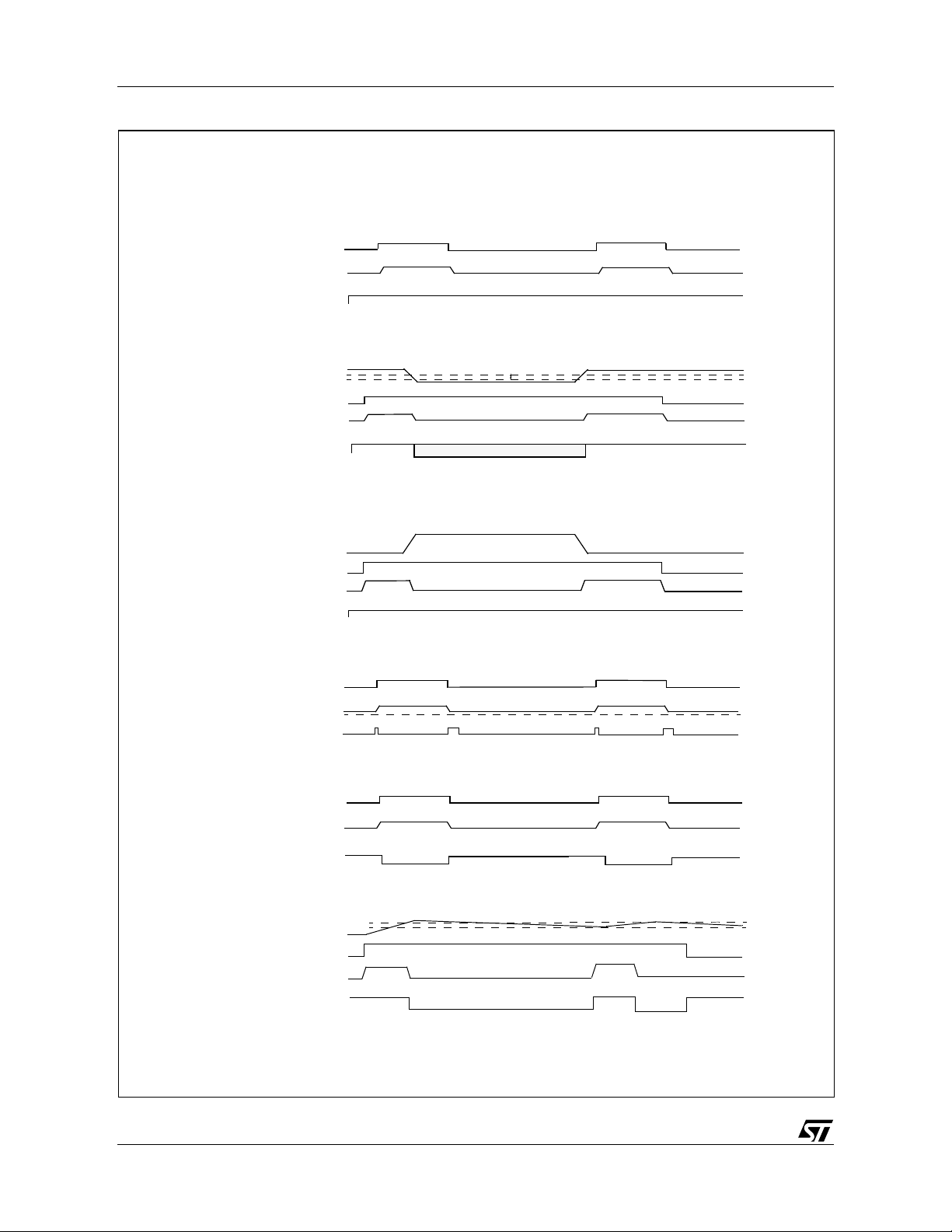
Figure 7. Waveforms
INPUT
n
OUTPUT VOLTAGE
STATUS
V
INPUT
OUTPUT VOLTAGE
STATUS
V
INPUT
OUTPUT VOLTAGE
STATUS
n
CC
n
n
CC
n
NORMAL OPERATION
n
UNDERVOLTAGE
V
USDhyst
V
USD
n
undefined
OVERVOLTAGE
VCC>V
VCC<V
OV
n
n
OV
INPUT
n
OUTPUT VOLTAGE
STATUS
INPUT
n
n
OUTPUT VOLTAGE
STATUS
T
INPUT
n
j
n
OUTPUT CURREN T
STATUS
n
OPEN LOAD with external pull-up
V
n
V
OL
OUT>VOL
OPEN LOAD without external pull-up
n
OVERTEMPERATURE
T
TSD
T
R
n
8/20
Page 9
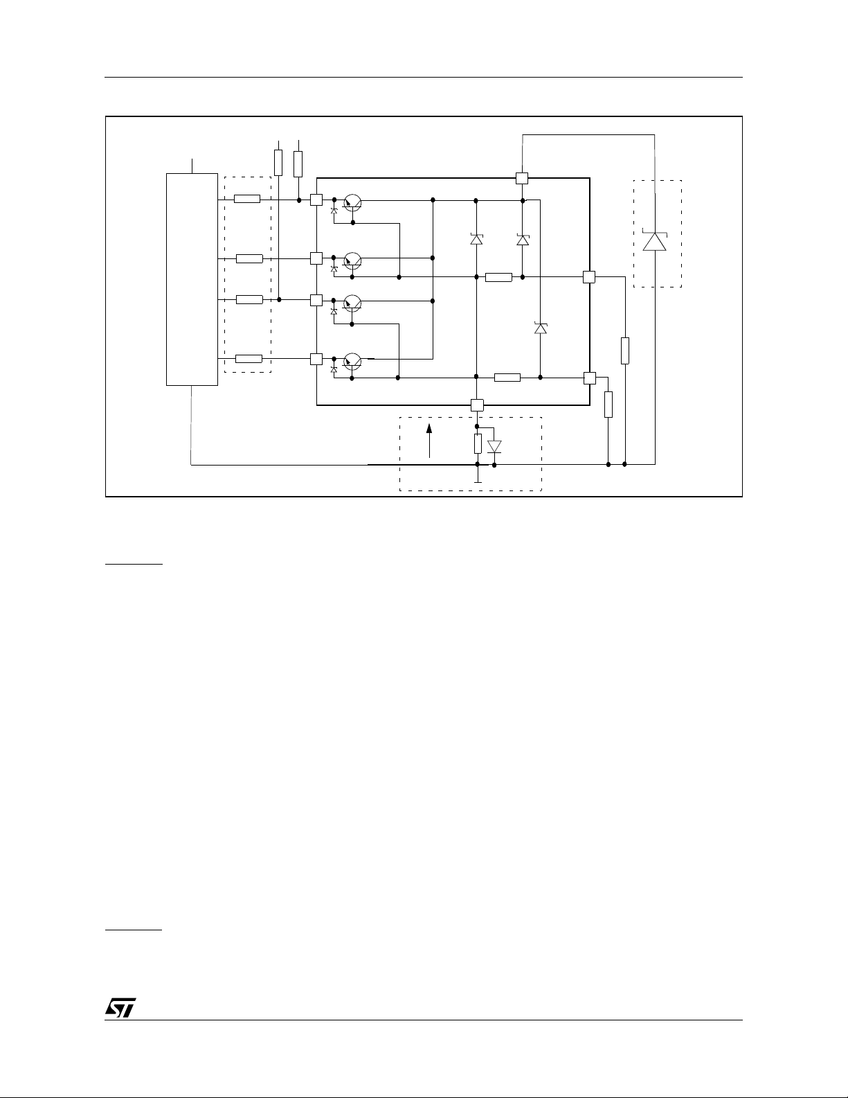
Figure 8. Application Schematic
+5V
+5V
+5V
R
prot
R
µ
C
prot
R
prot
R
prot
STATUS1
INPUT1
STATUS2
INPUT2
VND810MSP-E
V
CC
D
ld
OUTPUT1
GND PROTECTION NETWORK AGAINST
REVERSE BATTERY
Solution 1: Resist or in the ground line (R
can be used with any type of load.
The following is an indication on how to d imension the
resistor.
R
GND
1) R
2) R
where -I
be found in the absolute maximum rating section of the
≤ 600mV / I
GND
≥ (−VCC) / (-I
GND
is the DC reverse ground pin current and can
GND
S(on)max
GND
.
)
device’s datasheet.
Power Dissipatio n in R
battery situations) is:
= (-VCC)2/R
P
D
GND
(when VCC<0: during reverse
GND
This resistor can be shared amongst several different
HSD. Please note that the value of this resistor should be
calculated with formula (1) where I
sum of the maximum on-state currents of the different
S(on)max
devices.
Please note that if the microprocessor ground is not
common with the device ground then the R
produce a shift (I
and the status output values. This shift will vary
S(on)max
* R
) in the input threshold s
GND
depending on h ow many devic es are ON in the case of
several high side drivers sharing the same R
If the calculated power dissipation leads to a large
resistor or several devices have to share the same
resistor then the ST suggest to utilize Solution 2 (see
below).
Solution 2:
A resistor (R
D
GND
A diode (D
=1kΩ) should be inserted in parallel to
GND
if the device will be driving an inductive load.
) in the ground line.
GND
only). This
GND
becomes the
GND
.
GND
will
V
GND
GND
R
GND
D
OUTPUT2
GND
This small signal diode can be safely shared amongst
several different HS D. Also in this cas e, the presenc e of
the ground netwo rk will produce a shift (j600mV) in the
input threshold and the status output values if the
microprocessor ground is not common with the device
ground. This shift will not vary if more than one HSD
shares the same diode/resistor network.
Series resistor in INPUT and STATUS lines are also
required to prevent that, durin g battery voltage tra nsient,
the current exceeds the Absolute Maximum Rating.
Safest configurati on for unu sed INPU T and STA TUS pin
is to leave them unconnected.
LOAD DUMP PROTECTION
Dld is necessary (Voltage Transient Suppressor) if the
load dump peak voltage exceeds V
max DC rating.
CC
The same applies if the device will be subject to
transients on the V
line that are greater than the ones
CC
shown in the ISO T/R 7637/1 table.
µC I/Os PROTECTION:
If a ground protection network is used and negative
transient are present on the V
be pulled negative. ST suggests to insert a resistor (R
in line to prevent the µC I/Os pins to latch-up.
The value of these resistors is a compromise between
the leakage current of µC and the current required by the
HSD I/Os (Input levels compatibility) with the latch-up
limit of µC I/Os.
-V
CCpeak/Ilatchup
≤ R
prot
Calculation example:
For V
5kΩ ≤ R
CCpeak
prot
= - 100V and I
≤ 65kΩ.
line, the control pins will
CC
≤ (V
OHµC-VIH-VGND
≥ 20mA; V
latchup
) / I
OHµC
prot
IHmax
≥ 4.5V
)
9/20
Page 10
VND810MSP-E
U
S
Recommended R
value is 10kΩ.
prot
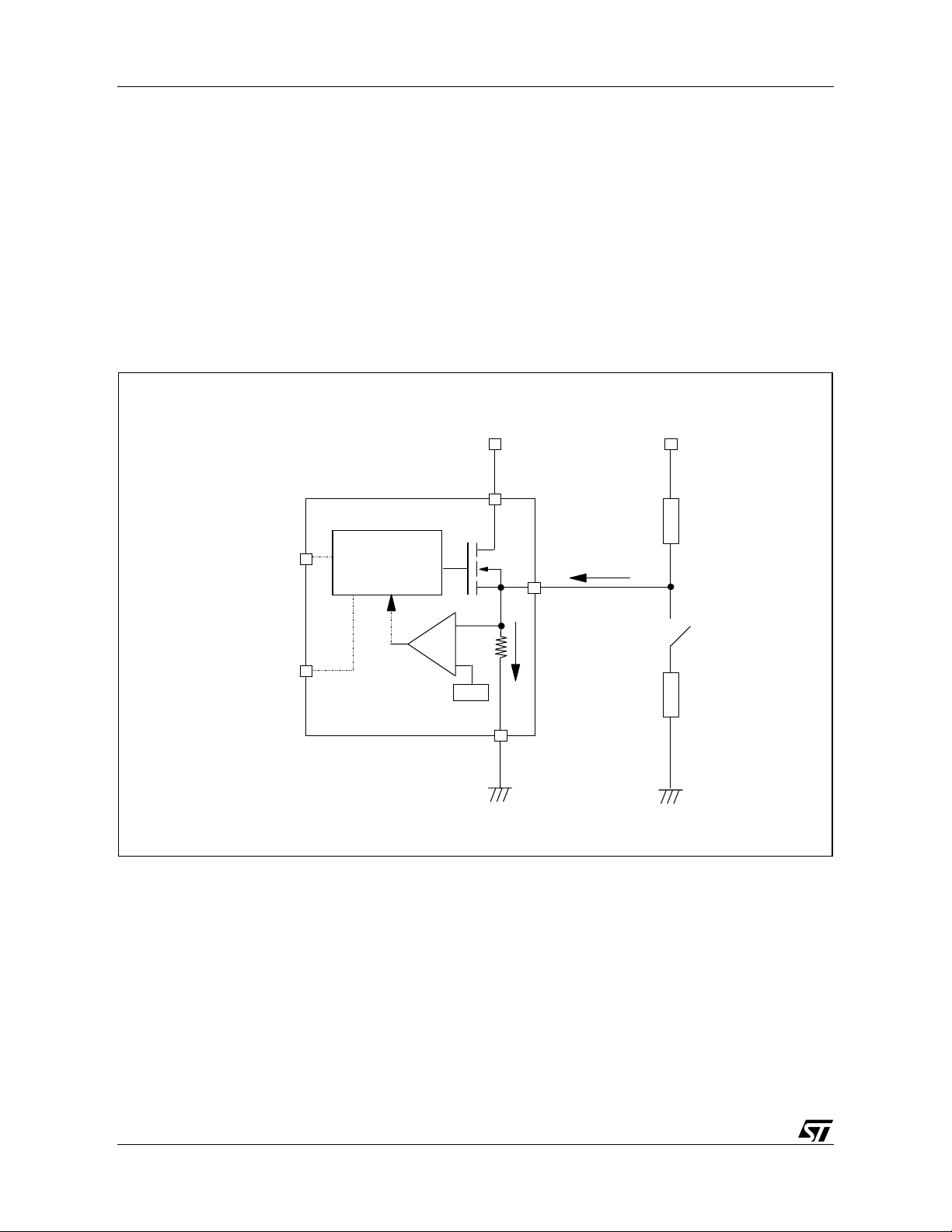
OPEN LOAD DETECTION IN OFF STATE
Off state open load detection require s an ex ter nal pull-u p
resistor (R
positive supply voltage (V
) connected between OUTPUT pin and a
PU
) like the +5V line used to
PU
supply the microprocessor.
The external resistor has to be selected according to the
following requirements:
1) no false open load indication when load is connected:
in this case we have to a void V
; this results in the following condition
V
Olmin
V
=(VPU/(RL+RPU))RL<V
OUT
to be higher than
OUT
Olmin.
Figure 9. Open Load Detection in Off State
INPUT
DRIVER
+
LOGIC
2) no misdetection when load is disconnected: in this
case the V
has to be higher than V
OUT
results in the following con dition RPU<(V
.
I
L(off2)
Because I
may significantly increase if V
s(OFF)
pulled high (up to several mA), the pull-u p resistor R
should be connected to a supply that is switched OFF
when the module is in standby.
The values of V
OLmin
, V
OLmax
and I
are available in
L(off2)
the Electrical Characteristics section.
V batt. VPU
V
CC
R
P
I
L(off2)
; this
OLmax
PU–VOLmax
out
)/
is
PU
TATUS
+
V
OL
GROUND
R
OUT
R
L
10/20
Page 11
VND810MSP-E
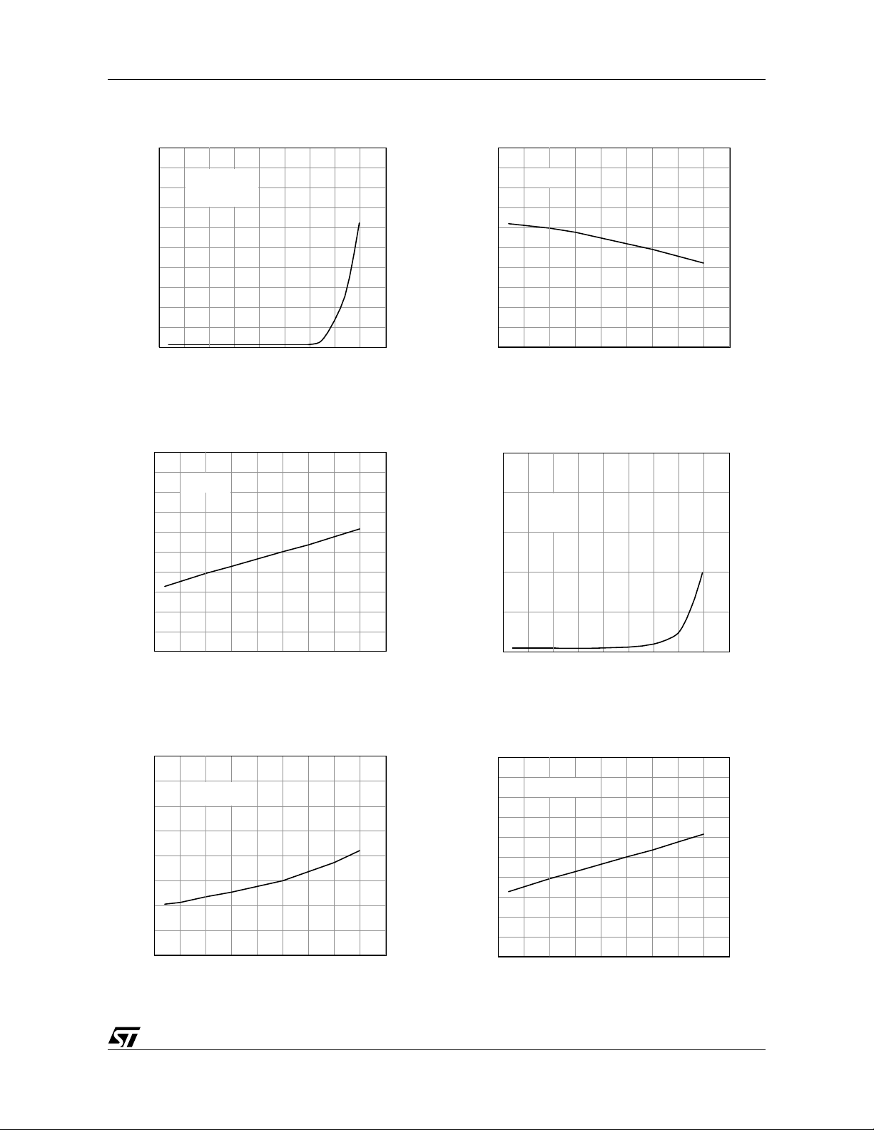
Figure 10. Off State Output Current
IL(off1) (uA)
1.6
1.44
1.28
1.12
0.96
0.8
0.64
0.48
0.32
0.16
0
-50 -25 0 25 50 75 100 125 150 175
Off state
Vcc=36V
Vin=Vout=0V
Tc (ºC)
Figure 11. Input Clamp Voltage
Vicl (V)
8
7.8
7.6
7.4
7.2
7
6.8
6.6
6.4
6.2
6
Iin=1mA
-50 -25 0 25 50 75 100 125 150 175
Tc (°C)
Figure 13. High Level Input Current
Iih (uA)
5
4.5
3.5
2.5
1.5
0.5
Vin=3.25V
4
3
2
1
0
-50 -25 0 25 50 75 100 125 150 175
Tc (°C)
Figure 14. Status Leakage Current
Ilstat (uA)
0.05
0.04
Vstat=5V
0.03
0.02
0.01
0
-50 -25 0 25 50 75 100 125 150 175
Tc (°C)
Figure 12. Status Low Output Voltage
Vstat (V)
0.8
0.7
Istat=1.6mA
0.6
0.5
0.4
0.3
0.2
0.1
0
-50 -25 0 25 50 75 100 125 150 175
Tc (°C)
Figure 15. Status Clamp Voltage
Vscl (V)
8
7.8
7.6
7.4
7.2
6.8
6.6
6.4
6.2
Istat=1mA
7
6
-50 -25 0 25 50 75 100 125 150 175
Tc (°C)
11/20
Page 12
VND810MSP-E
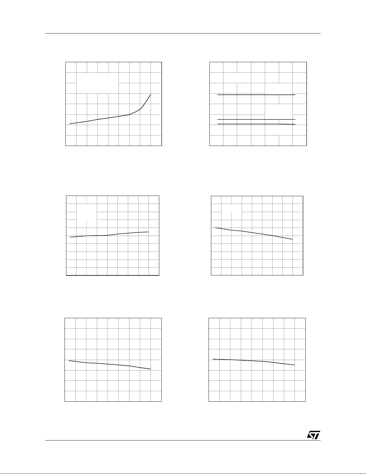
Figure 16. On State Resistance Vs T
case
Ron (mOhm)
400
350
300
250
200
150
100
50
0
-50 -25 0 25 50 75 100 125 150 175
Iout=1A
Vcc=8V; 13V & 36V
Tc (ºC)
Figure 17. Openload On State Detection
Threshold
Iol (mA)
60
55
50
45
40
35
30
25
20
15
10
Vcc=13V
Vin=5V
-50 -25 0 25 50 75 100 125 150 175
Tc (°C)
Figure 19. On State Resistance Vs V
CC
Ron (mOhm)
400
350
Iout=1A
300
250
200
150
100
Tc= 125ºC
Tc= 25ºC
Tc= - 40ºC
50
0
510152025303540
Vcc (V)
Figure 20. Openload Off State Detection
Threshold
Vol (V)
5
4.5
4
3.5
3
2.5
2
1.5
1
0.5
0
Vin=0V
-50 -25 0 25 50 75 100 125 150 175
Tc (°C)
Figure 18. Input High Level
Vih (V)
3.6
3.4
3.2
3
2.8
2.6
2.4
2.2
2
-50 -25 0 25 50 75 100 125 150 175
Tc (°C)
12/20
Figure 21. Input Low Level
Vil (V)
2.6
2.4
2.2
2
1.8
1.6
1.4
1.2
1
-50 -25 0 25 50 75 100 125 150 175
Tc (°C)
Page 13
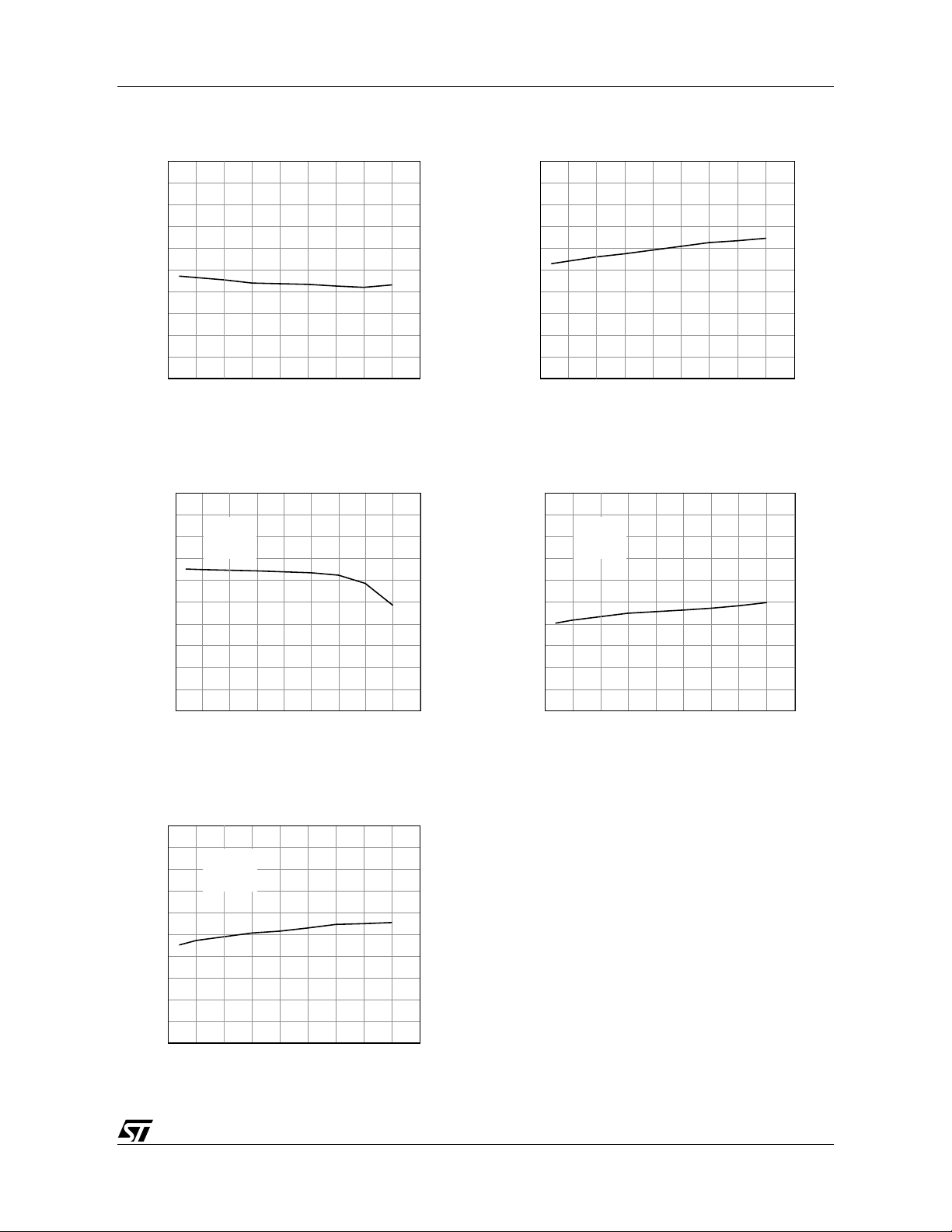
VND810MSP-E
Figure 22. Input Hysteresis Voltage
Vhyst (V)
1.5
1.4
1.3
1.2
1.1
1
0.9
0.8
0.7
0.6
0.5
-50 -25 0 25 50 75 100 125 150 175
Tc (°C)
Figure 23. Turn-on Voltage Slope
dVout/dt(on) (V/ms)
1000
900
800
700
600
500
400
300
200
100
Vcc=13V
Rl=13Ohm
0
-50 -25 0 25 50 75 100 125 150 175
Tc (ºC)
Figure 25. Overvoltage Shutdown
Vov (V)
50
48
46
44
42
40
38
36
34
32
30
-50 -25 0 25 50 75 100 125 150 175
Tc (°C)
Figure 26. Turn-off Voltage Slope
dVout/dt(off) (V/ms)
500
450
400
350
300
250
200
150
100
50
0
Vcc=13V
Rl=13Ohm
-50 -25 0 25 50 75 100 125 150 175
Tc (ºC)
Figure 24. I
LIM
Vs T
case
Ilim (A)
2
1.8
1.6
1.4
1.2
1
0.8
0.6
0.4
0.2
0
Vcc=13V
-50 -25 0 25 50 75 100 125 150 175
Tc (°C)
13/20
Page 14
VND810MSP-E
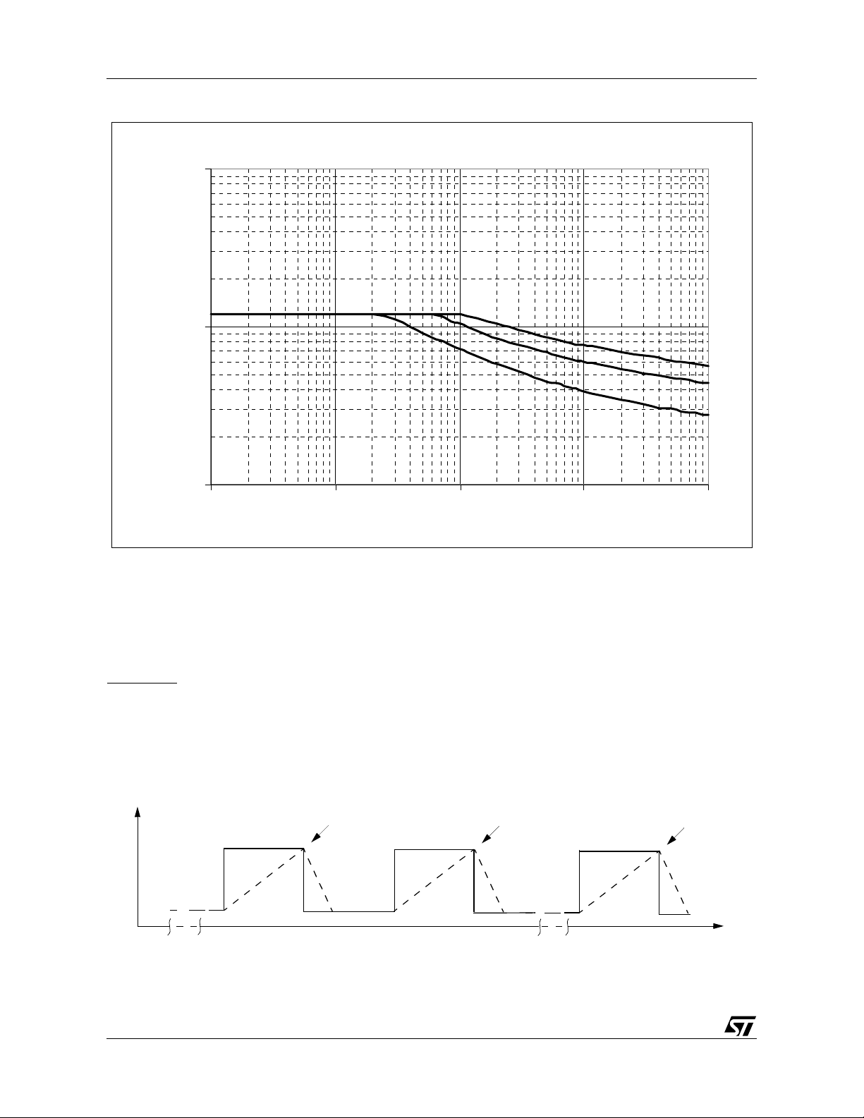
Figure 27. Maximum Turn Off Current Versus Load Inductance
LMAX (A)
I
10
A
1
B
C
0.1
1 10 100 1000 10000
A = Single Pulse at T
B= Repetitive pulse at T
C= Repetitive Pulse at T
Conditions:
VCC=13.5V
VIN, I
L
Jstart
=150ºC
=100ºC
Jstart
=125ºC
Jstart
Demagnetization
L(mH)
Values are generated with R
In case of repetitive pul s es, T
each demagnetization) of every pulse must not
exceed the temperature specified above for
curves B and C.
Demagnetization
=0Ω
L
(at beginning of
jstart
Demagnetization
14/20
t
Page 15
PowerSO-10™ Thermal Data
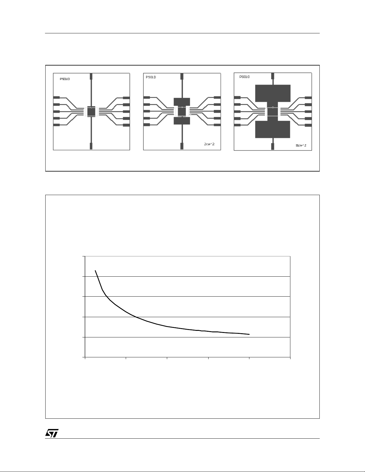
Figure 28. PowerSO-10™ PC Board
VND810MSP-E
Layout condition of Rth and Zth measurements (PCB FR4 area= 58mm x 58mm, PCB thickness=2mm,
Cu thickness=35µm, Copper areas: from minimum pad lay-out to 8cm
Figure 29. R
55
50
45
40
Vs PCB Copper Area in Open Box Free Air Condition
thj-amb
RTHj_amb (°C/W)
2
).
Tj-Tamb=50°C
35
30
0246810
PCB Cu heatsink area (cm^2)
15/20
Page 16
VND810MSP-E
Z
R
Z
1δ–
+
=
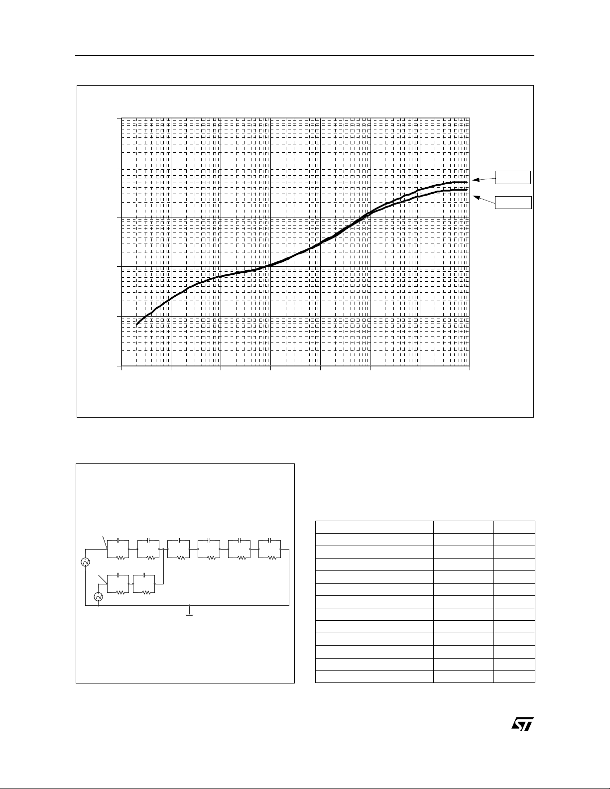
Figure 30. PowerSO-10 Thermal Impedance Junction Ambient Single Pulse
ZTH (°C/ W)
1000
100
10
1
0.1
0.01
0.0001 0.001 0.01 0.1 1 10 100 1000
Ti me (s)
Figure 31. Thermal Fitting Model of a Double
Channel HSD in PowerSO-10
Pulse Calculation Formula
δ
THδ
TH
⋅
THtp
()
Footprint
6 cm
2
where
δ tpT⁄=
Table 14. Thermal Parameter
Tj_1
Tj_2
16/20
C1
Pd1
C1 C2
R2
R1
Pd2
C3 C4
R3R1 R6R5R2
T_amb
C5 C6C2
R4
Area/island (cm2)Footprint6
R1 (°C/W) 0.05
R2 (°C/W) 0.3
R3( °C/W) 0.3
R4 (°C/W) 0.8
R5 (°C/W) 12
R6 (°C/W) 37 22
C1 (W.s/°C) 0.001
C2 (W.s/°C) 5.00E-03
C3 (W.s/°C) 0.02
C4 (W.s/°C) 0.3
C5 (W.s/°C) 0.75
C6 (W.s/°C) 3 5
Page 17
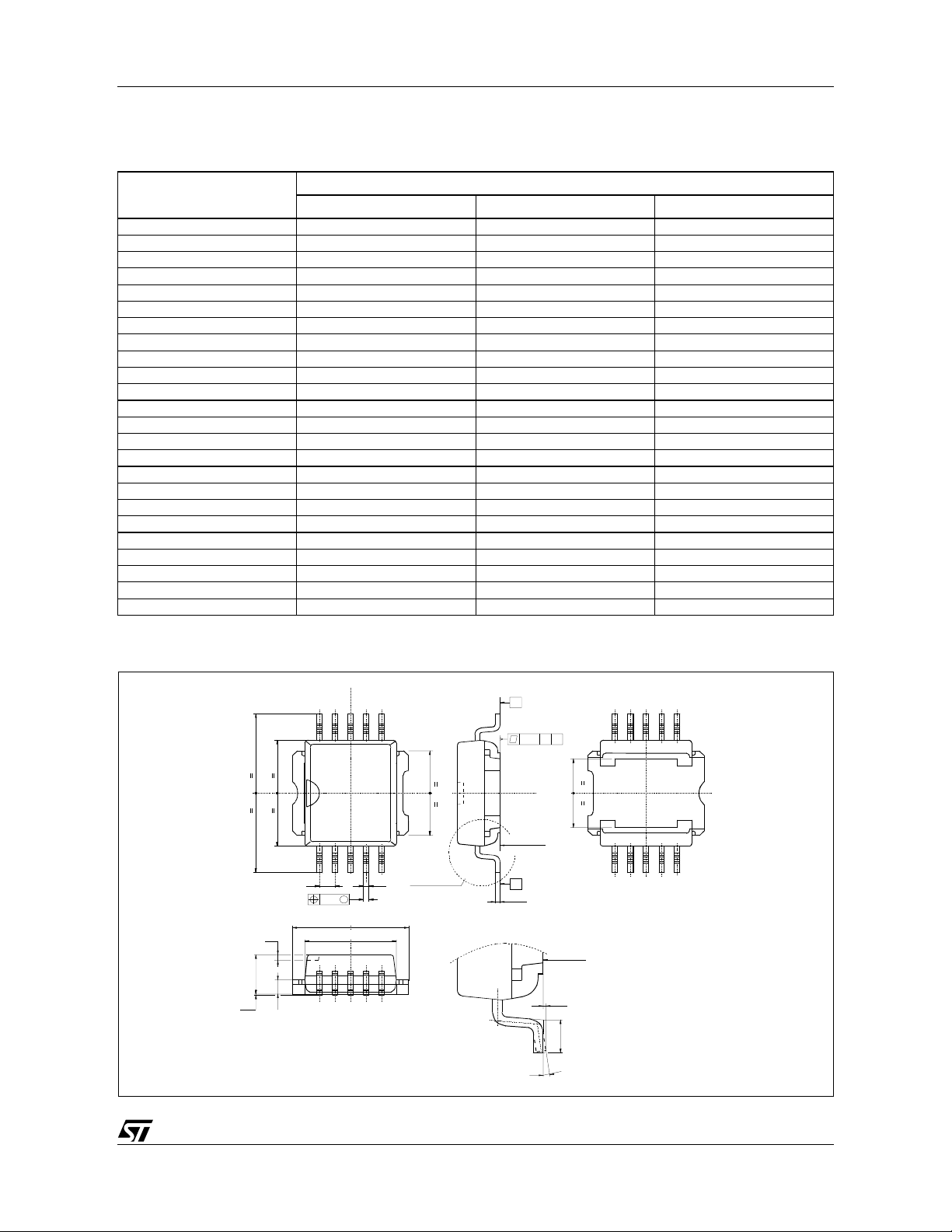
PACKAGE MECHANICAL
Table 15. PowerSO-10™ Mechanical Data
Symbol
A 3.35 3.65
A (*) 3.4 3.6
A1 0.00 0.10
B 0.40 0.60
B (*) 0.37 0.53
C 0.35 0.55
C (*) 0.23 0.32
D 9.40 9.60
D1 7.40 7.60
E 9.30 9.50
E2 7.20 7.60
E2 (*) 7.30 7.50
E4 5.90 6.10
E4 (*) 5.90 6.30
e1.27
F 1.25 1.35
F (*) 1.20 1.40
H 13.80 14.40
H (*) 13.85 14.35
h0.50
L 1.20 1.80
L (*) 0.80 1.10
a0º 8º
α (*) 2º 8º
Note: (*) Mu ar on l y PO A P013P
Min. Typ. Max.
VND810MSP-E
Millimeters
Figure 32. PowerSO-10™ Package Dimensions
10
HE
h
A
F
A1
1
eB
0.25
D
= =
D1
= =
E2
DETAIL "A"
DETAIL "A"
B
0.10 A
SEATING
PLANE
A
C
α
B
E4
SEATING
PLANE
A1
L
P095A
17/20
Page 18
VND810MSP-E
9
3
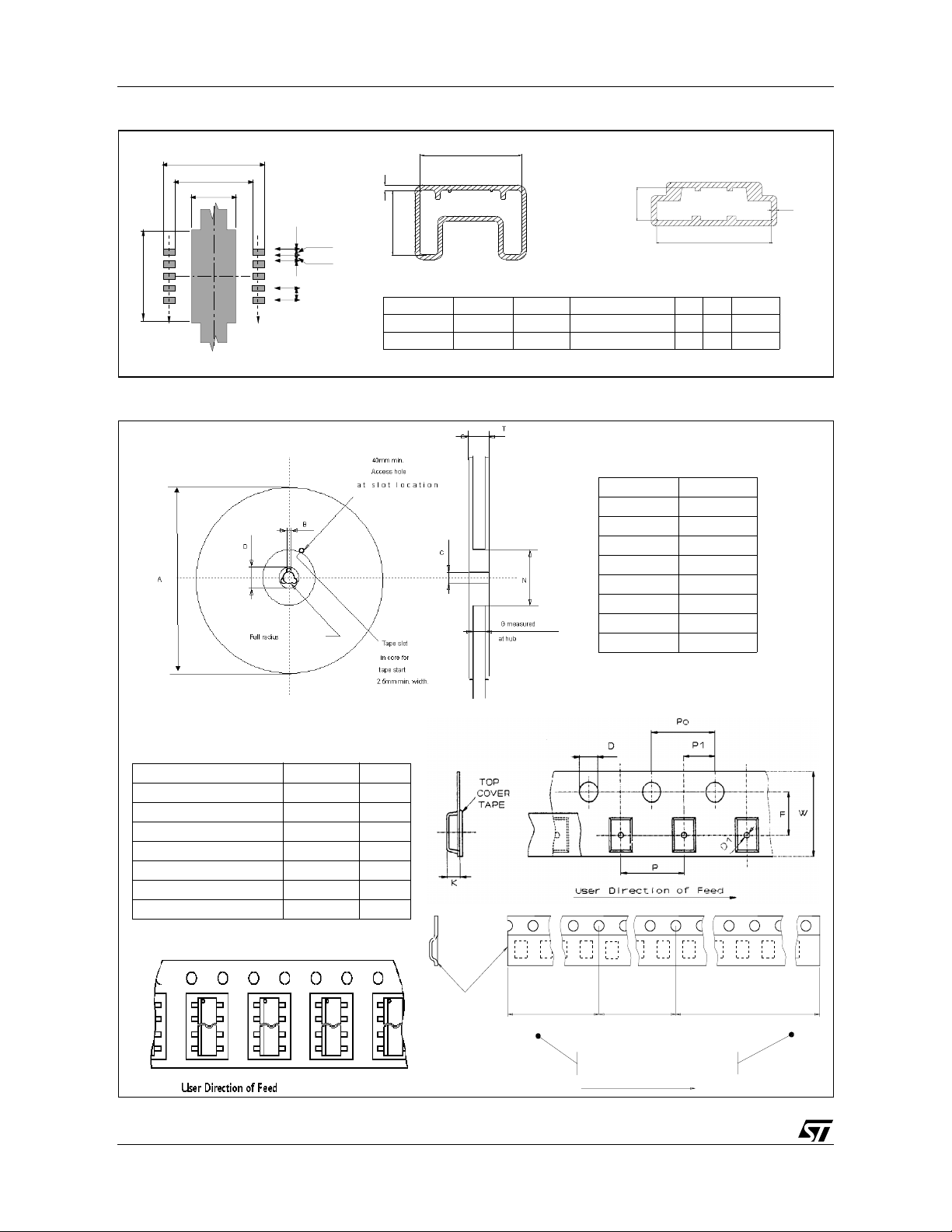
Figure 33. PowerSO-10™ Suggested Pad Layout and Tube ShipmenT (no suffix)
14.6 - 14.9
10.8 - 11
6.30
0.67 - 0.7
1
2
3
.5
4
5
10
0.54 - 0. 6
9
8
7
1.27
6
C
A
All dimensions are in mm.
Base Q.ty Bulk Q.ty Tube length (± 0.5) A B C (± 0.1)
Casablanca 50 1000 532 10.4 16.4 0.8
Muar 50 1000 532 4.9 17.2 0.8
Figure 34. TApe and Reel Shipment (suffix “TR”)
B
A
MUARCASABLANCA
C
B
REEL DIMENSIONS
Base Q.ty 600
Bulk Q.ty 600
A (max) 330
B (min) 1.5
C (± 0.2) 13
F 20.2
G (+ 2 / -0) 24.4
N (min) 60
T (max) 30.4
All dimensions are in mm.
TAPE DIMENSIONS
According to Electronic Industries Association
(EIA) Standard 481 rev. A, Feb. 1986
Tape width W 24
Tape Hole Spacing P0 (± 0.1) 4
Component Spacing P 24
Hole Diameter D (± 0.1/-0) 1.5
Hole Diameter D1 (min) 1.5
Hole Position F (± 0.05) 11.5
Compartment Depth K (max) 6.5
Hole Spacing P1 (± 0.1) 2
All dimensions are in mm.
18/20
Top
cover
tape
End
500mm min
Empty components p ockets
saled with cover tape.
User direction of feed
Start
No componentsNo components Compon ents
500mm min
Page 19

REVISION HISTORY
Date Revision Description of Changes
Oct. 2004 1 - First Issue.
Mar. 2005 2 - Power Outputs table correction.
VND810MSP-E
19/20
Page 20

VND810MSP-E
Information furnished is believed to be accurate and reliable. However, STMicroelectronics assumes no res ponsibility for the consequences
of use of such information nor for any infring ement of patents or other righ ts of third parties which may result from its use. No license is granted
by implication or otherwise under any patent or patent rights of STMicroelectronics. Specifications mentioned in this publication are subject
to change without notic e. This publication supersedes and replaces all infor m ation previously supplied. STMicroelectronics products are not
authorized for use as critical components in life support devices or systems without express written approval of STMicroelectronics.
The ST logo is a registered trademark of STMicroelectronics.
All other names are the property of their respective owners
© 2005 STMicroelectronics - All rights reserved
STMicroelectronics group of companies
Australia - Belgium - Brazil - Canada - China - Czech Republic - Finland - France - Germany - Hong Kong - India - Israel - Ita ly - Japan -
Malaysia - Malta - Morocco - Singapore - Spain - Sweden - Switzerland - United Kingdom - United States of America
www.st.com
20/20
 Loading...