

TEA3718
Stepper motor driver
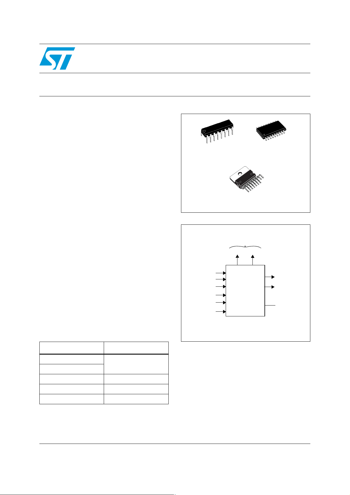
Features
■ Half-step and full-step mode
■ Bipolar drive of stepper motor for maximum
motor performance
■ Built-in protection diodes
■ Wide range of current control 5 to 1500 mA
■ Wide voltage range 10 to 50 V
■ Designed for unstabilized motor supply voltage
■ Current levels can be selected insteps or
varied continuously
■ Thermal overload protection
■ Alarm output or pre-alarm output
Applications
The TEA3718 is a bipolar monolithic integrated
circuit intended to control and drive the current in
one winding of a bipolar stepper motor.
Description
The circuits consist of an LS-TTL compatible logic
input, a current sensor, a monostable and an
output stage with built-in protection diodes. Two
TEA3718 ICs and a few external components
form a complete control and drive unit for LS-TTL
or microprocessor-controlled stepper motor
systems.
Table 1. Device summary
Power DIP 12+2+2
Multiwatt™ 15
Figure 1. Block diagram
Motor winding
OUT A
OUT B
COMPARATOR
INPUT
PHASE
PULSE TIME
IN0
IN1
REFERENCE
TEA3718
SO20
ALARM
(TEA3718SP)
PRE-ALARM
(TEA3718SFP)
SENSE
RESISTOR
Order code Package
TM: Multiwatt is a trademark of STMicroelectronics
E-TEA3718SDP
Power DIP
E-TEA3718DP
E-TEA3718SFP SO20
E-TEA3718SFPTR SO20 (tape and reel)
E-TEA3718SP Multiwatt™ 15
January 2009 Rev 2 1/26
www.st.com
26
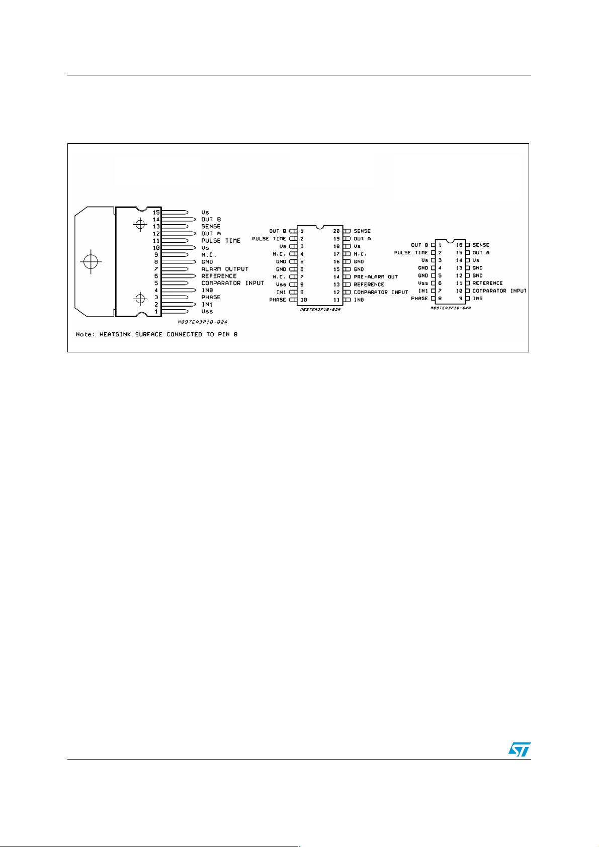
Pin connections
1 Pin connections
Figure 2. Package pin locations (top views)
E-TEA3718SP
(Multiwatt 15)
E-TEA3718SFP
(SO20)
E-TEA3718DP
E-TEA3718SDP
(Power DIP 12+2+2)
2/26

Contents
Contents
1 Pin connections . . . . . . . . . . . . . . . . . . . . . . . . . . . . . . . . . . . . . . . . . . . . . 2
2 Device diagrams . . . . . . . . . . . . . . . . . . . . . . . . . . . . . . . . . . . . . . . . . . . . 5
3 Electrical specifications . . . . . . . . . . . . . . . . . . . . . . . . . . . . . . . . . . . . . . 7
3.1 Absolute maximum ratings . . . . . . . . . . . . . . . . . . . . . . . . . . . . . . . . . . . . . 7
3.2 Recommended operating conditions . . . . . . . . . . . . . . . . . . . . . . . . . . . . . 7
3.3 Thermal data . . . . . . . . . . . . . . . . . . . . . . . . . . . . . . . . . . . . . . . . . . . . . . . 8
3.4 Electrical characteristics . . . . . . . . . . . . . . . . . . . . . . . . . . . . . . . . . . . . . . 10
4 Functional blocks . . . . . . . . . . . . . . . . . . . . . . . . . . . . . . . . . . . . . . . . . . 13
4.1 Alarm output (TEA3718SP, TEA3718DP and TEA3718SDP) . . . . . . . . . 14
4.2 Pre-alarm output (TEA3718SFP) . . . . . . . . . . . . . . . . . . . . . . . . . . . . . . . 15
4.3 Current reduction in alarm condition . . . . . . . . . . . . . . . . . . . . . . . . . . . . 15
4.4 Typical application . . . . . . . . . . . . . . . . . . . . . . . . . . . . . . . . . . . . . . . . . . 16
5 Functional description . . . . . . . . . . . . . . . . . . . . . . . . . . . . . . . . . . . . . . 17
5.1 Input logic . . . . . . . . . . . . . . . . . . . . . . . . . . . . . . . . . . . . . . . . . . . . . . . . . 17
5.2 Phase input . . . . . . . . . . . . . . . . . . . . . . . . . . . . . . . . . . . . . . . . . . . . . . . 17
5.3 Current sensor . . . . . . . . . . . . . . . . . . . . . . . . . . . . . . . . . . . . . . . . . . . . . 17
5.4 Single-pulse generator . . . . . . . . . . . . . . . . . . . . . . . . . . . . . . . . . . . . . . . 18
5.5 Output stage . . . . . . . . . . . . . . . . . . . . . . . . . . . . . . . . . . . . . . . . . . . . . . . 18
5.6 V
5.7 Analog control . . . . . . . . . . . . . . . . . . . . . . . . . . . . . . . . . . . . . . . . . . . . . 18
, VS and V
SS
R . . . . . . . . . . . . . . . . . . . . . . . . . . . . . . . . . . . . . . . . . . . . . . . . . . . . . . . . . 18
3/26

Contents
6 Application notes . . . . . . . . . . . . . . . . . . . . . . . . . . . . . . . . . . . . . . . . . . 19
6.1 Motor selection . . . . . . . . . . . . . . . . . . . . . . . . . . . . . . . . . . . . . . . . . . . . . 19
6.2 Unused inputs . . . . . . . . . . . . . . . . . . . . . . . . . . . . . . . . . . . . . . . . . . . . . 19
6.3 Interference . . . . . . . . . . . . . . . . . . . . . . . . . . . . . . . . . . . . . . . . . . . . . . . 19
6.4 Operating sequence . . . . . . . . . . . . . . . . . . . . . . . . . . . . . . . . . . . . . . . . . 20
7 Package mechanical data . . . . . . . . . . . . . . . . . . . . . . . . . . . . . . . . . . . . 21
Revision history . . . . . . . . . . . . . . . . . . . . . . . . . . . . . . . . . . . . . . . . . . . . . . . . . . . . 25
4/26
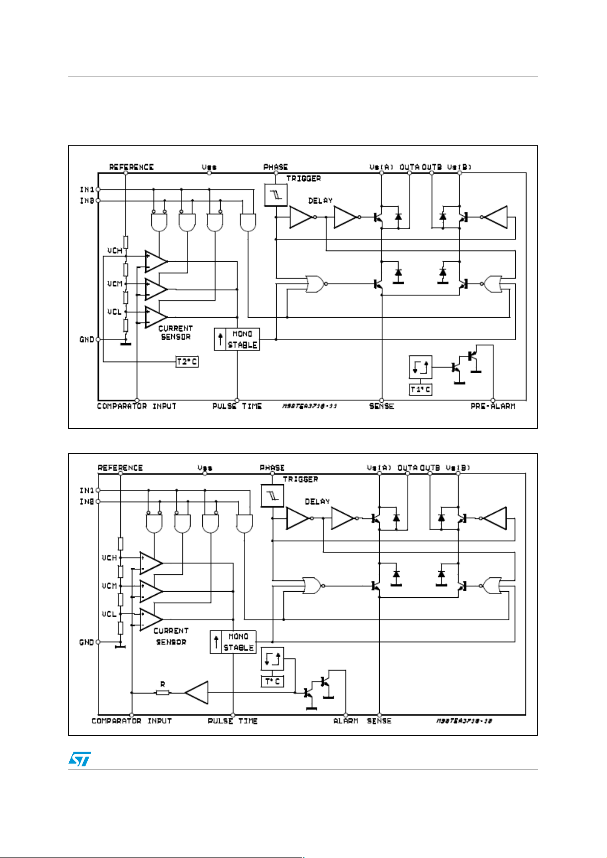
Device diagrams
2 Device diagrams
Figure 3. Detailed block diagram (TEA3718SFP)
Figure 4. Detailed block diagram (TEA3718SP)
5/26

Device diagrams
Table 2. Pin functions
Name Function
OUTB
Output connection (with pin OUT A). The output stage is a "H" bridge formed by four
transistors and four diodes suitable for switching applications.
A parallel RC network connected to this pin sets the OFF time of the lower power
PULSE TIME
V
(B) Supply voltage input for half output stage
S
GND
V
SS
transistors. The pulse generator is a monostable triggered by the rising edge of the
output of the comparators (t
= 0.69 RT CT).
off
Ground connection. In SO20 and power DIP these pins also conduct heat from die to
printed circuit copper.
Supply voltage input for logic circuitry
This pin and pin IN0 are logic inputs which select the outputs of three comparators to set
IN1
the current level. Current also depends on the sensing resistor and reference voltage.
Ta b l e 8 : Tr ut h ta bl e
See
.
This TTL-compatible logic input sets the direction of current flow through the load. A
PHASE
high level causes current to flow from OUT A (source) to OUT B (sink). A Schmidt trigger
on this input provides good noise immunity and a delay circuit prevents output stage
short circuits during switching.
IN0 See IN1
Input connected to the three comparators. The voltage across the sense resistor is
feedback to this input through the low pass filter RCCC. The lower power transistor are
COMPARATOR INPUT
disabled when the sense voltage exceeds the reference voltage of the selected
comparator. When this occurs the current decays for a time set by RT CT,
= 0.69 RT CT.
T
off
A voltage applied to this pin sets the reference voltage of the three comparators.
REFERENCE
Reference voltage with the value of R
output current.
(A) Supply voltage input for half output stage
V
S
OUTA See pin OUT B
and the two inputs IN0 and IN1 determines the
S
SENSE RESISTOR Connection to lower emitters of output stage for insertion of current sense resistor
ALARM When T
PRE-ALARM When T
reaches T1 oC the alarm output becomes low (TEA3718SP)
j
reaches T2 oC the pre-alarm output becomes low (T2<T1) (TEA3718SFP)
j
Table 3. Device comparison table
Device Current Package Alarm Pre-alarm
TEA3718SDP 1.5 A Power DIP 12+2+2 Not connected
TEA3718SFP 1.5 A SO20 Connected
TEA3718SP 1.5 A Multiwatt 15 Connected
TEA3718DP 1.5 A Power DIP 12+2+2 Not connected
6/26

Electrical specifications
3 Electrical specifications
3.1 Absolute maximum ratings
Table 4. Absolute maximum ratings
Symbol Parameters Value Unit
V
SS
V
S
Supply voltage
50
7
V
Input voltage:
V
I
– logic inputs
– analog inputs
– reference input
V
6
SS
15
V
Input current:
i
i
I
O
T
J
T
op
T
stg
– logic inputs
– analog inputs
-10
-10
mA
Output current ±1.5 A
Junction temperature +150
o
Operating ambient temperature range 0 to 70 oC
Storage temperature range -55 to +150 oC
C
3.2 Recommended operating conditions
Table 5. Recommended operating conditions
Symbol Parameters SO20 Power DIP Multiwatt 15 Unit
V
SS
Vs Supply voltage 10 - 45 V
Supply voltage 4.75 5 5.25 V
I
T
t
t
m
amb
r
f
Output current 0.020 - 1.2 A
Ambient temperature 0 - 70
o
Rise time for logic inputs - - 2 µs
Fall time for logic inputs - - 2 µs
7/26
C
Electrical specifications
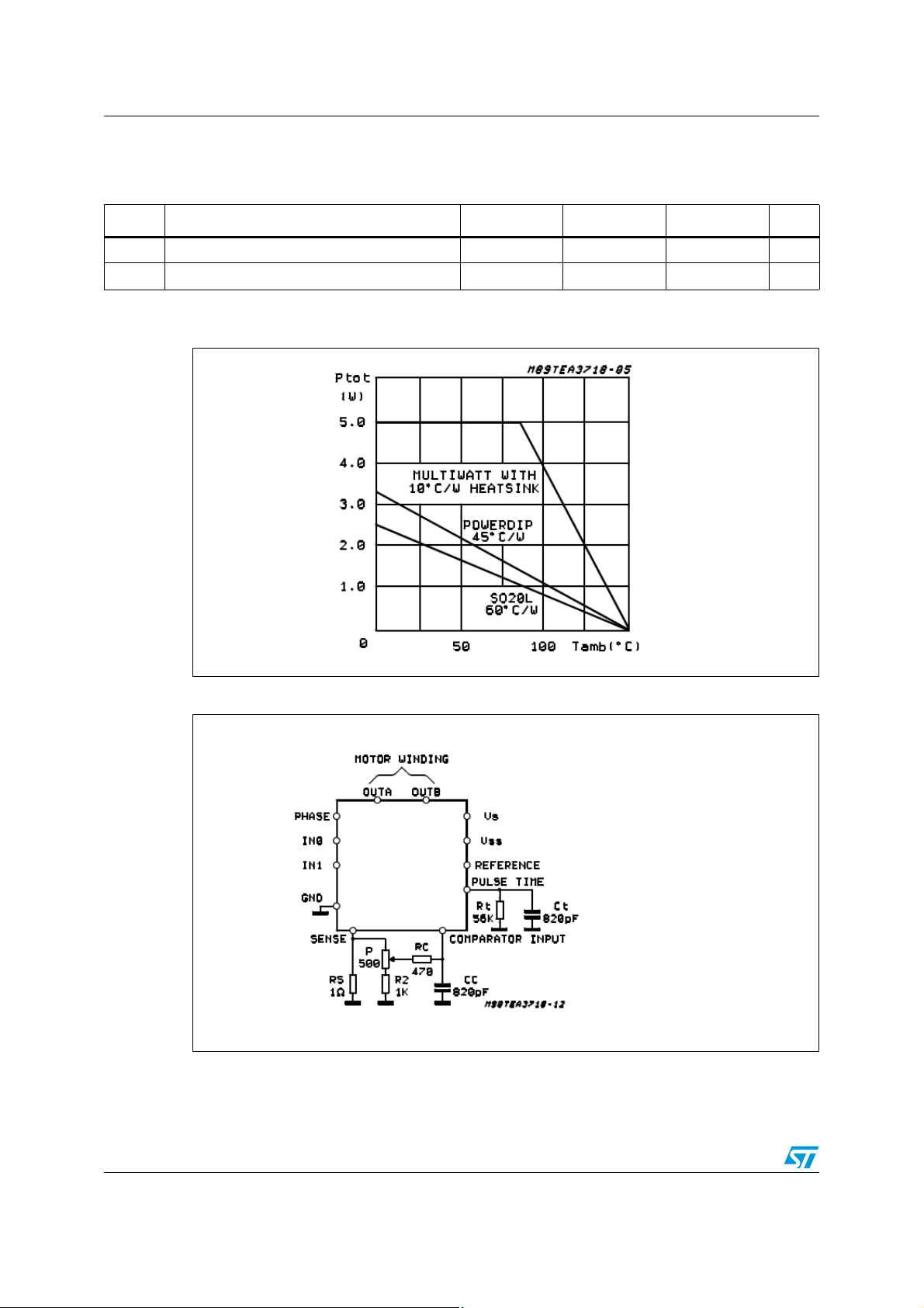
3.3 Thermal data
Table 6. Thermal data
Symbol Parameters SO20 Power DIP Multiwatt 15 Unit
(j-c) Maximum junction-case thermal resistance 16 11 3
R
th
R
(j-a) Maximum junction-ambient thermal resistance 60
th
1. Soldered on a 35 µm thick 4 cm2 PC board copper area
(1)
45
(1)
40
o
C/W
o
C/W
Figure 5. Maximum power dissipation
Figure 6. Typical external component configuration
RS = 1 ohm inductance free
= 470 ohms
R
C
CC = 820 pF ceramic
Rt = 56 kohms
Ct = 820 pF ceramic
P = 500 ohms
R2 = 1 kohm
8/26

Electrical specifications
Figure 7. Output waveforms
9/26

Electrical specifications
3.4 Electrical characteristics
Table 7. Electrical characteristics
Symbol Parameter Min.
I
Supply current - - 25 mA
CC
V
IH
V
IL
I
IH
I
IL
V
CH
High level input voltage - logic inputs 2 2 - - V
Low level input voltage - logic inputs - - 0.8 V
High level input current - logic inputs - - 20 µA
Low level input current - logic inputs (VI = 0.4 V) -0.4 - - mA
Comparator threshold voltage (VR = 5V)
VCM
V
CL
I
I
CO
off
Comparator input current -20 - 20 µA
Output leakage current (IO = 0, I1 = 1 T
(1)
(2)
IO = 0, I1 = 0
IO = 0, I1 = 0
I
= 0, I1 = 0
O
= 25oC) - - 100 µA
amb
390
230
65
Typ.
420
250
80
(2)
Max.
440
27090mV
Total saturation voltage drop (Im = 1 A)
V
(total)
sat
P
tot
t
off
t
d
(alarm) Alarm output saturation voltage IO = 2 mA (Multiwatt) - 0.8 - V
V
sat
I
ref
V
(source)
sat
Total power dissipation - Im = 1 A, fs = 30 kHz - 3.1 3.6 W
Cut off time (see
V
> 5 µs
ton
Turn off delay (see
Figure 6
Figure 6
and
and
Figure 7
Figure 7
dVC/dt > 50 mV/µs)
Reference input current, VR = 5 V - 0.4 1 mA
Source diode transistor pair
saturation voltage
SO20/Power DIP
Multiwatt
, Vmm = 10 V
) T
= 25oC,
amb
Power DIP I
= 0.5 A
m
Power DIP Im = 1 A
Multiwatt I
= 0.5 A
m
Multiwatt Im = 1 A
-
-
-
-
2.8
3.2
25 30 35 ms
-1.6-µs
-
-
-
-
1.05
1.35
-
-
1.2 (1.3)
1.5 (1.7)
1.3
1.7
(2)
Unit
V
V
V
I
(source) = 0.5 A - 1.1 1.5 (1.6)
Vf(source diode) Source diode forward voltage
f
V
If(source) = 1 A - 1.25 1.7 (1.9)
I
sub
Vsat(sink)
V
(sink diode) Sink diode forward voltage
f
1. Vs = Vss = 5 V, ± 5%, Vmm = 10 V to 45V, Tamb = 0 to 70oC (Tamb = 25oC for TEA3718SFP) unless otherwise specified.
2. Values in parentheses apply only to E-TEA3718SFP and E-TEA3718SFPTR mounted in SO20 package.
Substrate leakage current If = 1A - - 5 mA
Sink diode transistor pair
saturation
Power DIP I
= 0.5 A
m
Power DIP Im = 1 A
Multiwatt I
= 0.5 A
m
Multiwatt Im = 1 A
If(sink) = 0.5 A
If(sink) = 1 A
-
-
-
-
-
-
1
1.2
1
1.1
1.2 (1.3)
1.3 (1.5)
-
-
1.4 (1.6)
1.5 (1.9)
1.3
1.5
V
V
V
10/26

Electrical specifications
Figure 8. Sink driver VCE sat against I
Figure 9. Lower diode Vf against I
OUT
and T
out
and T
j
j
Figure 10. Source driver VCE sat against I
11/26
OUT
and T
j

Electrical specifications
Figure 11. Upper diode Vf against I
Figure 12. I
against junction temperature
ref
OUT
and T
j
Figure 13. Comparator input current against T
12/26
and V
j
C

Functional blocks
4 Functional blocks
Figure 14. Alarm output (TEA3718SP)
Figure 15. Pre-alarm output (TEA3718SFP)
13/26

Functional blocks
4.1 Alarm output (TEA3718SP, TEA3718DP and TEA3718SDP)
The ALARM output pin becomes low when the junction temperature reaches T ° C. When an
alarm condition occurs, parts of the supply voltage (dividing bridge R - R
comparator input pin (
Figure 16
). Depending on the RC value the behavior of the circuit on
an alarm condition is as follows:
● RC > 80 ohms, the output stage is switched off
● RC > 60 ohms, the current in the motor windings is reduced according to the
approximate formula: (see also
Figure 18
V
Im
----------
TH
RS
and
V
CC
------------ ------
RRC+
Figure 19
R
C
------- -
•–=
RS
)
) is fed to the
C
with V
= threshold of the comparator (VCH, VCM, VCL) R = 700 ohms (typical).
TH
For several Multiwatt packages a common detection can be obtained as in
Figure 16. Alarm detection for power DIP package
Figure 17
.
14/26

Functional blocks
Figure 17. Common detection for several Multiwatt packages
4.2 Pre-alarm output (TEA3718SFP)
When the junction temperature reaches T1° C (typically = 170 ° C) a pre-alarm signal is
generated on the PRE-ALARM output pin.
Soft thermal protection occurs when function temperature reaches T2 (T2 > T1).
4.3 Current reduction in alarm condition
Note: The resistance values given in this section are for the V
adjusted when using other comparator thresholds or V
Figure 18. Current reduction in the motor on alarm condition (typical curve)
threshold. They should be
CH
values.
ref
15/26

Functional blocks
Figure 19. Half-current on alarm condition circuit (Vref = 5V)
4.4 Typical application
Figure 20. Typical application circuit
16/26

Functional description
5 Functional description
The circuit is intended to drive a bipolar constant current through one motor winding. The
constant current is generated through switch mode regulation.
There is a choice of three different current levels with the two logic inputs lN0 and lN1. The
current can also be switched off completely.
5.1 Input logic
If any logic input is left open, the circuit treats it as a high-level input.
l
Table 8 . Truth t a b l e
IN0 IN1 Current level
H H No current
L H Low current
H L Medium current
L L Maximum current
5.2 Phase input
The PHASE input pin determines the direction of current flow in the winding, depending on
the motor connections. The signal is fed through a Schmidt trigger for noise immunity, and
through a time delay in order to guarantee that no short-circuit occurs in the output stage
during phase-shift. A high level on the PHASE input causes the motor current flow from
OUTA through the winding to OUTB.
The lH0 and lH1 input pins select the current level in the motor winding. The values of the
different current levels are determined by the reference voltage VR together with the value of
the sensing resistor R
5.3 Current sensor
This part contains a current sensing resistor (RS), a low pass filter (RC, CC) and three
comparators. Only one comparator is active at a time. It is activated by the input logic
according to the current level chosen with signals IN0 and IN1. The motor current flows
through the sensing resistor RS. When the current has increased so that the voltage across
RS becomes higher than the reference voltage on the other comparator input, the
comparator output goes high, which triggers the pulse generator and its output goes high
during a fixed pulse time (t
causing the motor current to decrease during t
.
S
), thus switching off the power feed to the motor winding, and
off
off
.
17/26

Functional description
5.4 Single-pulse generator
The pulse generator is a monostable triggered on the positive going edge of the comparator
output. The monostable output is high during the pulse time, t
timing components R
and CT. toff = 0.69 ⋅ RT C
T
T
, which is determined by the
off
The single pulse switches off the power feed to the motor winding, causing the winding
current to decrease during t
. If a new trigger signal should occur during t
off
, it is ignored.
off
5.5 Output stage
The output stage contains four Darlington transistors and four diodes, connected in an Hbridge. The two sinking transistors are used to switch the power supplied to the motor
winding, thus driving a constant current through the winding.
Note: It is not permitted to short circuit the outputs.
5.6 VSS, VS and V
R
The circuit stands any order of turn-on or turn-off the supply voltages VSS and VS. Normal
dV/dt values are then assumed.
Preferably, V
should track VSS during power on and power off if VS is established.
R
5.7 Analog control
The current levels can be varied continuously if VR is varied with a circuit varying the voltage
on the comparator terminal.
Figure 21. Power losses against
output current
18/26

Application notes
6 Application notes
6.1 Motor selection
Some stepper motors are not designed for continuous operation at maximum current. As the
circuit drives a constant current through the motor, its temperature might increase
excessively both at low and high speed operation.
Also, some stepper motors have such high core losses that they are not suited for switch
mode current regulation.
6.2 Unused inputs
Unused inputs should be connected to proper voltage levels in order to get the highest noise
immunity.
6.3 Interference
As the circuit operates with switch mode current regulation, interference generation
problems might arise in some applications. A good measure might then be to decouple the
circuit with a 15 nF ceramic capacitor, located near the package between power
line V
S and ground. The ground lead between R
short as possible. This applies also to the lead between the sensing resistor R
See
Section 4: Functional blocks
.
, CC and circuit GND should be kept as
S
and point S.
S
19/26

Application notes
6.4 Operating sequence
Figure 22. Principal operating sequence
20/26

Package mechanical data
7 Package mechanical data
In order to meet environmental requirements, ST offers these devices in different grades of
ECOPACK® packages, depending on their level of environmental compliance. ECOPACK®
specifications, grade definitions and product status are available at:
ECOPACK® is an ST trademark.
www.st.com
.
21/26

Package mechanical data
22/26

Package mechanical data
23/26

Package mechanical data
24/26

Revision history
Revision history
Table 9. Document revision history
Date Revision Changes
24-Jan-2006 1 Initial release.
21-Jan-2009 2
Document reformatted.
Added
Figure 1
.
25/26

Please Read Carefully:
Information in this document is provided solely in connection with ST products. STMicroelectronics NV and its subsidiaries (“ST”) reserve the
right to make changes, corrections, modifications or improvements, to this document, and the products and services described herein at any
time, without notice.
All ST products are sold pursuant to ST’s terms and conditions of sale.
Purchasers are solely responsible for the choice, selection and use of the ST products and services described herein, and ST assumes no
liability whatsoever relating to the choice, selection or use of the ST products and services described herein.
No license, express or implied, by estoppel or otherwise, to any intellectual property rights is granted under this document. If any part of this
document refers to any third party products or services it shall not be deemed a license grant by ST for the use of such third party products
or services, or any intellectual property contained therein or considered as a warranty covering the use in any manner whatsoever of such
third party products or services or any intellectual property contained therein.
UNLESS OTHERWISE SET FORTH IN ST’S TERMS AND CONDITIONS OF SALE ST DISCLAIMS ANY EXPRESS OR IMPLIED
WARRANTY WITH RESPECT TO THE USE AND/OR SALE OF ST PRODUCTS INCLUDING WITHOUT LIMITATION IMPLIED
WARRANTIES OF MERCHANTABILITY, FITNESS FOR A PARTICULAR PURPOSE (AND THEIR EQUIVALENTS UNDER THE LAWS
OF ANY JURISDICTION), OR INFRINGEMENT OF ANY PATENT, COPYRIGHT OR OTHER INTELLECTUAL PROPERTY RIGHT.
UNLESS EXPRESSLY APPROVED IN WRITING BY AN AUTHORIZED ST REPRESENTATIVE, ST PRODUCTS ARE NOT
RECOMMENDED, AUTHORIZED OR WARRANTED FOR USE IN MILITARY, AIR CRAFT, SPACE, LIFE SAVING, OR LIFE SUSTAINING
APPLICATIONS, NOR IN PRODUCTS OR SYSTEMS WHERE FAILURE OR MALFUNCTION MAY RESULT IN PERSONAL INJURY,
DEATH, OR SEVERE PROPERTY OR ENVIRONMENTAL DAMAGE. ST PRODUCTS WHICH ARE NOT SPECIFIED AS "AUTOMOTIVE
GRADE" MAY ONLY BE USED IN AUTOMOTIVE APPLICATIONS AT USER’S OWN RISK.
Resale of ST products with provisions different from the statements and/or technical features set forth in this document shall immediately void
any warranty granted by ST for the ST product or service described herein and shall not create or extend in any manner whatsoever, any
liability of ST.
ST and the ST logo are trademarks or registered trademarks of ST in various countries.
Information in this document supersedes and replaces all information previously supplied.
The ST logo is a registered trademark of STMicroelectronics. All other names are the property of their respective owners.
© 2009 STMicroelectronics - All rights reserved
STMicroelectronics group of companies
Australia - Belgium - Brazil - Canada - China - Czech Republic - Finland - France - Germany - Hong Kong - India - Israel - Italy - Japan -
Malaysia - Malta - Morocco - Singapore - Spain - Sweden - Switzerland - United Kingdom - United States of America
www.st.com
26/26
 Loading...