


®
查询STV8207供应商
®
for A2 and NICAM Television/Video Recorders
Key Features
■ Full-Automatic Multi-Standard Demodulation
● B / G / I / L / M / N / D / K Standards
● Mono AM and FM
● FM 2-Carrier (German and Korean Zweiton) and
NICAM
■ Multi-Channel Capability
● 3 I²S digital inputs, S/PDIF (in/out)
● 5.1 analog outputs
● Dolby® Pro Logic®
● Dolby® Pro Logic II®
■ Sound Processing
● ST royalty-free processing: ST WideSurround, ST
OmniSurround, ST Dynamic Bass, SRS® WOW™,
SRS® TruSurround XT™ which is Virtual Dolby®
Surround and Virtual Dolby® Digital compliant
● Independent Volume / Balance for Loudspeakers
and Headphone
● Loudspeakers: Smart Volume Control (SVC),
5-band equalizer and loudness
● Headphone: Smart Volume Control (SVC), Bass-
Treble, Loudness and SRS® Tru B a s s™
■ Analog Audio Matrix
● 4 stereo inputs
● 3 stereo outputs
● THRU mode
■ Audio Delay for Audio Video Synchronization
● Embedded stereo delay up to 120 ms for lip-sync
function (up to 180 ms for tuner input)
● Independent delay on headphone and loudspeaker
channels
The STV82x7 family, based on audio digital signal
processors (DSP), performs high quality and advanced
dedicated digital audio processing.These devices
provide all of the necessary resources for automatic
detection and demodulation of analog audio
transmissions for European and Asian terrestrial TV
broadcasts.
STV82x7
Digital Audio Decoder/Processor
PRELIMINARY DATA
Virtual or true, multi-channel capabilities and easy digital
links make them ideal for digital audio low cost consumer
applications. Starting from enhanced stereo up to
independent control of 5 loudspeakers and a subwoofer
(5.1 channels), the STV82x7 family offers standard and
advanced features plus sound enhancements, spatial
and virtual effects to enhance television viewer comfort
and entertainment.
Typical Applications
● Analog and digital TV with virtual surround sound
● Analog and digital TV with multi-channel surround
sound
● DVD and HDD recorders
● “Palm size” portable TV
7
x
2
8
V
T
S
© 2004 SRS Labs, Inc. All rights reserved, SRS and
the SRS logo are registered trademarks of SRS Labs, Inc.
“Dolby”, “Pro Logic”, and the double-D symbol are trademarks of
Dolby Laboratories.
Rev. 3
February 2005 1/149

Block Diagram
LS_L
Loudspeakers
LS_C
LS_R
LS_SUB
Headphone / Surround
HP_LSS_L
HP_LSS_R
SC1_OUT_L
SC1_OUT_R
SC2_OUT_L
SC2_OUT_R
SC3_OUT_L
SC3_OUT_R
SCART
STV82x7
Outputs
™
Trubass
®
Bass/Treble, SRS
RMS
2 V
Stereo
DAC
Audio
Loudspeakers
Digital Audio Processing
RMS
0.9 V
DAC
Audio
Stereo
™
®,
®
Pro Logic
Pro Logic II
®
®
Dolby
Dolby
Volume, Equalizer, Balance,
ST WideSurround, ST Dynamic Bass,
ST OmniSurround,
Loudness,Smart Volume Control,
or TruSurround XT
™
WOW
Bass Management, Beeper
®
SRS
RMS
0.9 V
DAC
Audio
Stereo
Headphone
Digital Audio Processing
Volume, Balance, Loudness,
Smart Volume Control,
Digital Audio Matrix
In / Out
S/PDIF
Pre-scaler
Output
Analog
2 V
RMS
RMS
2 V
Audio
Matrix
Management
Power Supply
XTALOUT
XTALIN
Clock
Generator
CLK_SEL
clocks
I²S
data
I²S
Interface
Digital
FM/AM
NICAM
FM 2-carrier
Demodulation
A/D
IRQ
Logic
Control
AGC
SIF
Detection
Headphone
Sound IF
2/149
Mono Input
A/D
Audio
Input
Audio
Analog
SC2_IN_L
SC1_IN_L
MONO_IN
SC1_IN_R
SC2_IN_R
I²C
Interface
I²C
SCL SDA
Matrix
SC3_IN_L
SC4_IN_L
SC3_IN_R
SC4_IN_R
SCART
Inputs

STV82x7
Table of Contents
Chapter 1 General Description . . . . . . . . . . . . . . . . . . . . . . . . . . . . . . . . . . . . . . . . . . . . . . . .6
1.1 STV82x7 Overview ..............................................................................................................8
1.1.1 Core Features ............................................................................................................................................8
1.1.2 Software Information .................................................................................................................................9
1.1.3 Device Input Modes ...................................................................................................................................9
1.1.4 Electrical Features ...................................................................................................................................10
1.2 Typical Applications ...........................................................................................................10
1.3 Pin Descriptions and Application Diagrams .......................................................................14
Chapter 2 System Clock . . . . . . . . . . . . . . . . . . . . . . . . . . . . . . . . . . . . . . . . . . . . . . . . . . . .20
Chapter 3 Digital Demodulator . . . . . . . . . . . . . . . . . . . . . . . . . . . . . . . . . . . . . . . . . . . . . . .21
3.1 Sound IF Signal ..................................................................................................................21
3.2 Demodulation .....................................................................................................................22
Chapter 4 Dedicated Digital Signal Processor (DSP) . . . . . . . . . . . . . . . . . . . . . . . . . . . . .24
4.1 Back-end Processing .........................................................................................................24
4.2 Audio Processing ...............................................................................................................25
4.3 ST WideSurround ...............................................................................................................28
4.4 ST OmniSurround ..............................................................................................................28
4.5 Dolby Pro Logic II Decoder ................................................................................................28
4.6 Bass Management .............................................................................................................28
4.6.1 Bass Management Configuration 0 .........................................................................................................29
4.6.2 Bass Management Configuration 1 .........................................................................................................30
4.6.3 Bass Management Configuration 2 .........................................................................................................31
4.6.4 Bass Management Configuration 3 .........................................................................................................32
4.6.5 Bass Management Configuration 4 .........................................................................................................33
4.7 SRS WOW and TruSurround XT ......................................................................................33
4.7.1 SRS TruSurround ....................................................................................................................................33
4.7.2 SRS WOW ...............................................................................................................................................34
4.8 Smart Volume Control (SVC) .............................................................................................34
4.9 ST Dynamic Bass ..............................................................................................................35
4.10 5-Band Audio Equalizer .....................................................................................................35
4.11 Bass/Treble Control ...........................................................................................................35
4.12 Automatic Loudness Control ..............................................................................................36
4.13 Volume/Balance Control ....................................................................................................36
4.14 Soft Mute Control ...............................................................................................................37
3/149

STV82x7
4.15 Beeper ................................................................................................................................37
Chapter 5 Analog Audio Matrix (In / Out) . . . . . . . . . . . . . . . . . . . . . . . . . . . . . . . . . . . . . . .39
Chapter 6 I²S Interface (In / Out) . . . . . . . . . . . . . . . . . . . . . . . . . . . . . . . . . . . . . . . . . . . . . .40
6.1 I²S Inputs ............................................................................................................................40
6.2 I²S Output ...........................................................................................................................41
Chapter 7 S/PDIF Input/Output . . . . . . . . . . . . . . . . . . . . . . . . . . . . . . . . . . . . . . . . . . . . . . .42
Chapter 8 Power Supply Management . . . . . . . . . . . . . . . . . . . . . . . . . . . . . . . . . . . . . . . . .43
8.1 Standby Mode (Loop-through mode) .................................................................................43
Chapter 9 Additional Controls and Flag . . . . . . . . . . . . . . . . . . . . . . . . . . . . . . . . . . . . . . .44
9.1 Headphone Detection ........................................................................................................44
9.2 IRQ Generation ..................................................................................................................44
9.3 I²C Bus Expander ...............................................................................................................44
Chapter 10 STV82x7 Reset . . . . . . . . . . . . . . . . . . . . . . . . . . . . . . . . . . . . . . . . . . . . . . . . . . .45
Chapter 11 I²C Interface . . . . . . . . . . . . . . . . . . . . . . . . . . . . . . . . . . . . . . . . . . . . . . . . . . . . . .46
11.1 I²C Address and Protocol ...................................................................................................46
11.2 Start-up and Configuration Change Procedure ..................................................................47
Chapter 12 Register List . . . . . . . . . . . . . . . . . . . . . . . . . . . . . . . . . . . . . . . . . . . . . . . . . . . . .48
12.1 I²C Register Map ................................................................................................................49
12.2 STV82x7 General Control Registers ..................................................................................55
12.3 Clocking 1 ..........................................................................................................................56
12.4 Demodulator .......................................................................................................................59
12.5 Demodulator Channel 1 .....................................................................................................62
12.6 Demodulator Channel 2 .....................................................................................................66
12.7 NICAM Registers ...............................................................................................................71
12.8 Stereo Mode .......................................................................................................................73
12.9 Analog Control ...................................................................................................................74
12.10 Clocking 2 ..........................................................................................................................76
12.11 DSP Control .......................................................................................................................77
4/149

STV82x7
12.12 Automatic Standard Recognition ........................................................................................81
12.13 Audio Preprocessing and Selection Registers ...................................................................85
12.14 Matrixing .............................................................................................................................93
12.15 Audio Processing ...............................................................................................................98
12.16 5-Band Equalizer / Bass-Treble for Loudspeakers ..........................................................112
12.17 Headphone Bass-Treble ..................................................................................................113
12.18 Volume .............................................................................................................................116
12.19 Beeper ..............................................................................................................................126
12.20 Mute .................................................................................................................................127
12.21 S/PDIF ..............................................................................................................................128
12.22 Headphone Configuration ................................................................................................128
12.23 DAC Control .....................................................................................................................129
12.24 AutoStandard Coefficients Settings .................................................................................130
Chapter 13 Electrical Characteristics . . . . . . . . . . . . . . . . . . . . . . . . . . . . . . . . . . . . . . . . .132
13.1 Absolute Maximum Ratings ............................................................................................132
13.2 Thermal Data ..................................................................................................................132
13.3 Power Supply Data ..........................................................................................................132
13.4 Crystal Oscillator .............................................................................................................133
13.5 Analog Sound IF Signal ..................................................................................................133
13.6 SIF to I²S Output Path Characteristics .............................................................................134
13.7 SCART to SCART Analog Path Characteristics ..............................................................134
13.8 SCART and MONO IN to I²S Path Characteristics ..........................................................135
13.9 I2S to LS/HP/SUB/C Path Characteristics .......................................................................135
13.10 I²S to SCART Path Characteristics ..................................................................................136
13.11 MUTE Characteristics ......................................................................................................136
13.12 Digital I/Os Characteristics ...............................................................................................136
13.13 I²C Bus Characteristics ..................................................................................................137
13.14 I2S Bus Interface ..............................................................................................................138
Chapter 14 Input/Output Groups . . . . . . . . . . . . . . . . . . . . . . . . . . . . . . . . . . . . . . . . . . . . .140
Chapter 15 Package Mechanical Data . . . . . . . . . . . . . . . . . . . . . . . . . . . . . . . . . . . . . . . .145
Chapter 16 Revision History . . . . . . . . . . . . . . . . . . . . . . . . . . . . . . . . . . . . . . . . . . . . . . . .146
5/149

General Description STV82x7
1 General Description
The STV82x7 is a multistandard TV sound demodulator and audio processor which integrates
SRS® WOW™, SRS® TruSurround XT™, Dolby® Pro Logic®, Dolby® Pro Logic II®,Virtual
Dolby® Surround (VDS) and Virtual Dolby® Digital (VDD) capability.
ST advanced algorithms such as ST OmniSurround, ST WideSurround, ST Dynamic Bass are
also available in this audio sound processor. ST OmniSurround is a certified Dolby® algorithm for
the Virtual Dolby® Digital (VDD) and the Virtual Dolby® Surround (VDS). When using VDD or
VDS, either a Dolby® Digital or a Pro Logic® (or Pro Logic II®) decoder is mandatory
respectively.
This chip performs automatic multistandard analog TV stereo sound identification and
demodulation (no specific I²C programming is required). It offers various audio processing
functions such as equalization, loudness, beeper, volume, balance, and surround effects. It provides
a cost-effective solution for analog and digital TV designs.
The STV82x7 is perfectly suited to current and future digital TV platforms, based on audio/video
digital chips (STD2000, (DTV100 platform) and the future WorldWide iDTV one chip) which
include an internal digital decoder (MPEG, Dolby® Digital...). In the case where a Dolby® Digital
decoder is embedded in the audio/video digital chip, Virtual Dolby® Digital could be obtained.
For the CTV100/120 platform, the device is offered as an alternative solution to the first-generation
chassis that uses the STV82x6.
6/149

STV82x7 General Description
®
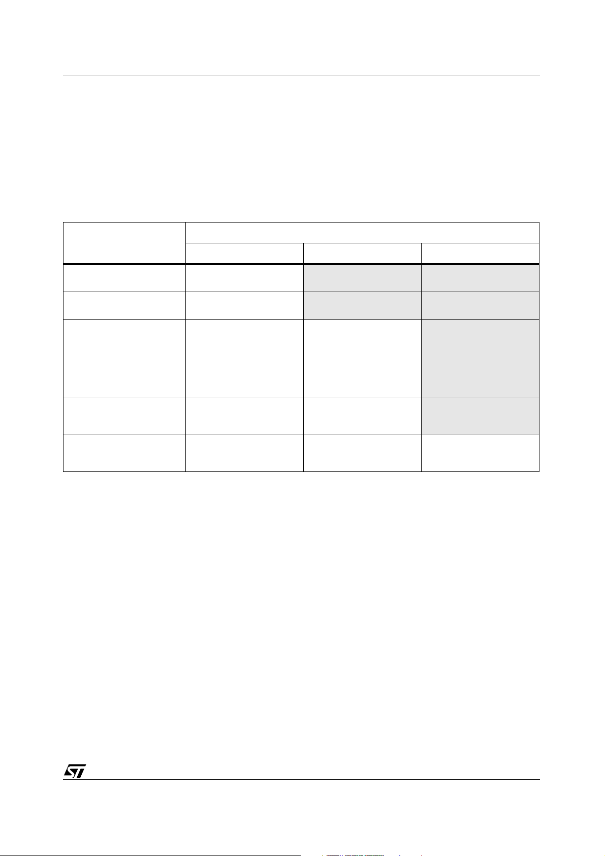
Table 1: STV82x7 Version List
STV8247 STV8257 STV8267 STV8277 STV8287
Demodulation
AM/FM - Mono, FM 2-carrier
NICAM
Multi-Channel Capability
3 x I²S In or 1 I²S Out,
S/PDIF (Pass-thru)
5.1 Analog Out for Loudspeakers
Virtual Dolby® Surround
Virtual Dolby® Digital capability
Dolby® Pro Logic®
Dolby® Pro Logic II®
Audio Processing
SRS® WOW™
SRS® TruSurround XT™
ST Voice, ST Dynamic Bass,
ST WideSurround
ST OmniSurround
2
S
T
T
V
V
8
8
2
2
1
0
7
7
T
T
V
V
8
8
2
2
3
2
7
7
S
S
S
S
T
S
T
V
8
2
4
7
D
S
V
T
8
V
2
8
4
2
7
5
D
7
S
X
S
S
T
T
V
V
8
8
2
2
5
5
7
7
D
D
S
X
S
T
S
T
V
8
2
6
7
D
S
V
T
8
V
2
8
6
2
7
7
D
7
S
X
S
T
S
V
T
8
V
2
8
7
2
7
7
D
7
S
D
X
XXXXXXXXXXXXXXXX
X XXXXXXXXXXXXX
XXX XXXXX
XXXXXXX
XX XXXX XXXX
1
XXX XXXXX
XX XX
XX
XXXXX
XXXXXXXXXXXXXXXX
XXXXXXXXXXXX
S
T
S
V
T
8
V
2
8
8
2
7
8
D
7
S
D
X
XX
1. Virtual Dolby Digital capability is obtained with the use of external Dolby Digital decoder (for
example STD05x0).
2. When using VDD or VDS with ST OmniSurround or SRS TruSurround XTTM, either a Dolby®
Digital or a Pro Logic® (or Pro Logic II®) decoder is mandatory respectively.
Figure 1: Package Ordering Information
Order Code:
STV82x7 (Tray)
STV82x7/T (Tape & Reel)
0
8
P
F
Q
T
For Example: STV8257DSX/T will be delivered in Tape & Reel conditioning
7/149

General Description STV82x7
1.1 STV82x7 Overview
1.1.1 Core Features
● Single audio source processing:
— IF source and/or analog stereo input (SCART)
— one digital source with a maximum of 6 synchronous channels (5.1 is obtained across three
I²S)
● SIF input signal with Automatic Gain Control (AGC)
● Digital Demodulator with automatic standard detection and demodulation for AM, FM mono,
FM 2 carriers (German or Korean FM 2-carrier) and NICAM
● Audio processor working at 32 kHz, 44.1 kHz or 48 kHz with specific features:
— For Loudspeakers (L, R, L
Dolby® Pro Logic II ® Decoder with Bass Management
SRS® WOW™ or TruSurround XT™ including Virtual Dolby® Surround and Virtual Dolby®
Digital
ST WideSurround
ST OmniSurround
ST Dynamic Bass
5-band Equalizer or Bass-Treble
Loudness
Smart Volume Control
Volume/Balance/Soft-mute
Beeper
Video Processing Delay Compensation
— For Headphone:
SRS® Tr u B a s s ™
Smart Volume Control
Bass-Treble
Loudness
Volume/Balance/Soft-mute
Beeper
Video Processing Delay Compensation
● Shared outputs for headphone and loudspeakers (surround channels);
● Analog matrix with:
— five external inputs:
four SCART inputs (2 V
one analog mono input (0.5 V
— one internal input from a digital matrix via a DAC
— three external outputs (2 V
— one internal output for the digital matrix (using an internal ADC)
● Digital matrix with:
— three input modes (Demodulator/SCART, SCART only and I²S)
— three stereo outputs (Loudspeakers, Headphone and SCART)
● High-end audio DAC
● S/PDIF output for connection with an external amplifier/decoder
● Internal multiplexer for the S/PDIF output (to share the internal S/PDIF output and the S/PDIF
output generated by the external decoder of the digital broadcast)
, RS, SubW, C):
S
capable)
RMS
RMS
capable)
RMS
)
8/149
STV82x7 General Description
● Specific stand-by mode (Loop-through)
● Control by I²C bus (two I²C addresses)
● System PLL and Clock Generation using either a single quartz oscillator or a differential clock
input
1.1.2 Software Information
The different software combinations are listed in Tab l e 2 .
Table 2: Input/Output Software Configurations
Output (Number of Channels)
Input (Number of Channels)
2 (+1) 4 (+1) 5 (+1)
1
2 (L and R)
2 (LT and RT)
4 (+1)
5 (+1)
ST WideSurround or
SRS® WOW™
ST WideSurround or
SRS® WOW™
ST WideSurround or
SRS® TruSurround XT™ or
ST OmniSurround or
Dolby® Pro Logic® + SRS®
TruSurround XT™ or
Dolby® Pro Logic® + ST
OmniSurround
SRS® TruSurround XT™ or
ST OmniSurround or
Downmix
SRS® TruSurround XT™or
ST OmniSurround or
Downmix
Dolby® Pro Logic®
No processing
Downmix No processing
Note: In addition to the above sound processing, it is always possible to add ST Voice and also ST
Dynamic Bass algorithms.
Note: The SRS® TruSurround® and ST OmniSurround are approved by Dolby as Virtual Dolby Surround
(VDS) and Virtual Dolby Digital (VDD).
The SRS® TruSurround XT™ system is composed of:
● SRS® TruSurround®
● SRS® WOW™
The SRS® WOW™ system also includes:
● SRS® Dialog Clarity™
● SRS® TruBass™
1.1.3 Device Input Modes
● Demodulator and SCART Mode (with output f
● SCART Only Mode (with output f
● I²S Mode (with output f
= 48 kHz)
S
= 32, 44.1 or 48 kHz)
S
9/149
= 32 kHz)
S

General Description STV82x7
— External audio input interface using 3 x I²S (for decoded streams such as Dolby® Digital
and/or standard stereo streams)
1.1.4 Electrical Features
Multi Power Supply: 1.8 V, 3.3 V and 8 V.
Power Consumption:
● lower than 1 W in Functional mode (full features)
● 200 mW in Loop-through mode corresponding to Switch-off of all digital blocks
1.2 Typical Applications
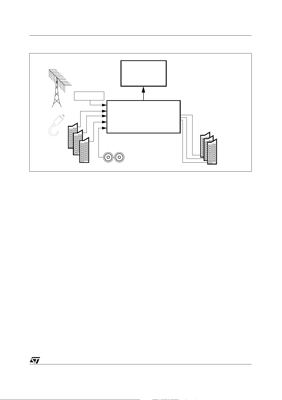
The STV82x7 is specified to enable flexible, analog and digital TV chassis design (refer to Figure 2,
Figure 3, Figure 4 and Figure 5).
The main considerations are:
● all necessary connections between devices can be provided through the TV set,
● pseudo stand-by mode used to copy to VCR or the DVD sources when the TV set is OFF,
● possible application compatibility with STV82x6 (TQFP80 package) TV design,
● pin-to-pin compatibility with STV82x8 (TQFP80 package) TV design.
The STV82x7 is used to process a single audio source (analog or digital). However, it is possible to
process two audio sources simultaneously using an STV82x7 interconnection (two chips can be
easily connected).
In the case of a single audio source, it is possible to hear and record in the same time: the same
audio stream can be simultaneously output on headphone, loudspeakers, S/PDIF and the SCART
connectors.
Note: Headphone and loudspeakers can be used simultaneously for dual-language purposes or for
different sound settings (e.g. volume). In this case, certain restrictions occur (see Section 4.2: Audio
Processing).
For more connections, the SCART-to-SCART path can be used. The use of these full analog paths
implies that the sound is not digitally processed.
10/149

STV82x7 General Description
Figure 2: STV8237 Typical Application (Enhanced Stereo)
or
Tu ne r
STV8237
Multistandard Demodulation
- FM 2-carrier and NICAM
Sound Processing
- Volume, Balance, 5-Band Equalizer
- ST WideSurround
- SRS® WOW™
Left Right
Figure 3: STV8247 Typical Application (Analog Virtual Sound)
R
SubW
L
Tu ne r
STV8247
Multistandard Demodulation
or
Left Right
1. When using VDS with ST OmniSurround or SRS TruSurround XTTM, a Pro Logic® decoder is mandatory.
- FM 2-carrier and NICAM
Sound Processing
- Volume, Balance, 5-Band Equalizer
- SRS® TruSurround XT™
- ST OmniSurround
- Virtual Dolby® Surround
1
R
SubW
L
11/149

General Description STV82x7
Figure 4: STV8257 Typical Application (Digital: Virtual Sound)
Multi-Channel Digital Decoder
or
(Dolby® Digital)
I²S
Tuner
Left Right
S/PDIF Pass-thru
STV8257
Multistandard Demodulation
- FM 2-carrier and NICAM
Audio Processing
- Volume, Balance, 5-Band Equalizer
- SRS® TruSurround XT™
- ST OmniSurround
- Virtual Dolby® Surround
- Virtual Dolby® Digital2
1
SubW
R
L
1. When using VDS with ST OmniSurround or SRS TruSurround XTTM, a Pro Logic® decoder is mandatory.
2. When using VDD with ST OmniSurround or SRS TruSurround XTTM, a Dolby® Digital decoder is mandatory.
Figure 5: STV8277 Typical Application (Digital TV: Multi-Channel and Virtual Sound)
Multi-Channel Digital Decoder
or
(Dolby® Digital)
I²S
Tuner
S/PDIF Pass-thru
STV8277
Multistandard Demodulation
- FM 2-carrier and NICAM
Audio Processing
SubW
R
RS
C
LS
L
- Volume, Balance, 5-Band Equalizer
- Dolby® Pro Logic II®
- 5.1 Analog Outputs
- SRS® TruSurround XT™
- Virtual Dolby® Surround
- Virtual Dolby® Digital
1
2
Left Right
1. When using VDS with ST OmniSurround or SRS TruSurround XTTM, a Pro Logic® decoder is mandatory.
2. When using VDD with ST OmniSurround or SRS TruSurround XT
12/149
TM
, a Dolby® Digital decoder is mandatory.
STV82x7 General Description
Figure 6: STV8217 Typical Application (Digital Recorder)
MPEG Codec
or
Tuner
I²S
STV8217
Multistandard Demodulation
- FM 2-carrier and NICAM
Left Right
13/149
General Description STV82x7
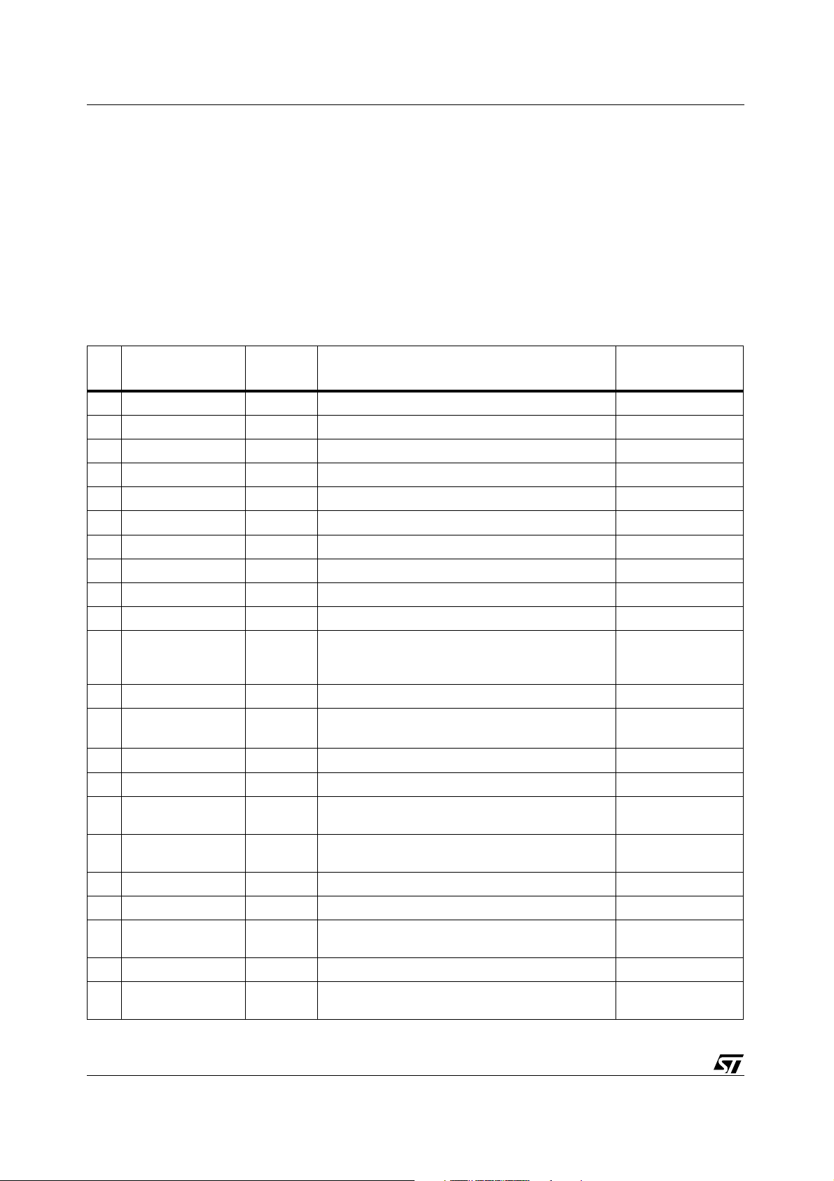
1.3 Pin Descriptions and Application Diagrams
● AP = Analog Power
● DP = Digital Power
● I= Input
● O = Output
● OD = Open-Drain
● B = Bi-Directional
● A = Analog
Table 3: TQFP80 Pin Description (Sheet 1 of 3)
Pin
No.
1 SC1_OUT_L A SCART1 Audio Output Left AO1L
2 SC1_OUT_R A SCART1 Audio Output Right AO1R
3 VCC_H AP 8V Power for Audio I/O & ESD Not connected
4 GND_H AP High Current Ground for Audio Outputs Connected to Ground
5 SC3_OUT_L A SCART3 Audio Output Left Not connected
6 SC3_OUT_R A SCART3 Audio Output Right Not connected
7 VCC33_SC AP 3.3V Power for Audio Buffers & DAC / ADC VDDC
8 GND33_SC AP Ground for Audio Buffers & DAC / ADC GNDC
9 SC1_IN_L A SCART1 Audio Input Left AI1L
10 SC1_IN_R A SCART1 Audio Input Right AI1R
11 VREFA A
12 GND_SA AP Ground for DACs Connected to Ground
13 VBG A
14 SC2_IN_L A SCART2 Audio Input Left AI2L
STV82x7
Pin Name
Typ e
(STV82x7)
Function for STV82x7
(Function for STV82x6 in italic characters)
Audio Bias Voltage Decoupling 1.55V
(Switched V
(VMCP))
Bandgap Voltage Reference Decoupling 1.2V
(V
decoupling pin for Audio Converters (VMC))
REF
decoupling pin for Audio Converters
REF
STV82x6
Pin Name
VMC1
VMC2
15 SC2_IN_R A SCART2 Audio Input Right AI2R
16 VCC33_LS AP
17 GND33_LS AP
18 SC2_OUT_L A SCART2 Audio Output Left AO2L
19 SC2_OUT_R A SCART2 Audio Output Right AO2R
20 VCC_NISO AP
21 VSS33_CONV AP Ground for DAC 1.8 to 3.3V Converters Connected to Ground
22 VDD33_CONV AP
3.3V Power for Audio DACs
(3.3V Power Supply for Audio Buffers and SCART)
Ground for Audio DACs
(Ground for Audio Buffers and SCART)
Polarization of the NISO (connected to 3.3V)
(8V / 5V Power supply for SCART & Audio buffers)
3.3V Power for DAC 1.8 to 3.3V Converters
(Voltage Reference for Audio buffers)
VDDA
GNDAH
VDDH
VREFA
14/149

STV82x7 General Description
Table 3: TQFP80 Pin Description (Sheet 2 of 3)
Pin
No.
23 SC3_IN_L A SCART3 Audio Input Left AI3L
24 SC3_IN_R A SCART3 Audio Input Right AI3R
25 SCL_FLT A SCART Filtering Left Not connected
26 SCR_FLT A
27 LS_C A Center Output Not connected
28 LS_L A Left Loudspeaker Output LSL
29 LS_R A Right Loudspeaker Output LSR
30 LS_SUB A Subwoofer Output SW
31 HP_LSS_L A Left Headphone Output or Left Surround Output HPL
32 HP_LSS_R A Right Headphone Output or Right Surround Output HPR
33 VSS18_CONV DP
34 VDD18_CONV DP 1.8V Power for Digital part of the DAC/ADC Not connected
35 HP_DET
36 ADR_SEL I Hardware Address selection for I²C Bus ADR
37 VSS18 DP Ground for Digital part Connected to Ground
STV82x7
Pin Name
Typ e
(STV82x7)
I Headphone Detection HPD
(Function for STV82x6 in italic characters)
SCART Filtering Right
(Bandgap Voltage Source Decoupling)
Ground for Digital part of the DAC/ADC
(Substrate Analog/Digital Shield)
Function for STV82x7
STV82x6
Pin Name
BGAP
GNDSA
38 VDD18 DP 1.8V Power for Digital part Not connected
39 SCL OD I²C Clock Input SCL
40 SDA OD I²C Data I/O SDA
41 VSS18 DP Ground for Digital part Connected to Ground
42 VDD18 DP
43 RST
44 S/PDIF_IN I
45 S/PDIF_OUT O
46 VDD33_IO1 DP 3.3V Power for Digital part VDD1
47 VSS33_IO1 DP Ground for Digital part GND1
48 CK_TST_CTRL D To be Grounded Not connected
49 VSS18 DP Ground for Digital part GNDSP
50 VDD18 DP 1.8V Power for Digital part Not connected
51 CLK_SEL I Clock Input Format Selection Not connected
52 XTALIN_CLKXTP I
I Main Reset Input RESET
1.8V Power for Digital part
(5V Power Regulator Control)
Serial Audio Data Input
(System Clock output)
Serial Audio Data Output
(I²S Master Clock output)
Crystal Oscillator Input or Differential Input Positive
(Crystal Oscillator Input)
REG
SYSCK
MCK
XTI
15/149

General Description STV82x7
Table 3: TQFP80 Pin Description (Sheet 3 of 3)
Pin
No.
53 XTALOUT_CLKXTM O
54 VCC18_CLK1 AP
55 GND18_CLK1 AP Ground for Clock PLL Analog & Crystal Oscillator 1/2 GNDP
56 GND18_CLK2 AP Ground for Clock PLL Digital 1/2 GND2
57 VCC18_CLK2 DP
58 VSS33_IO2 DP Ground for Digital IO pins 60 to 69 Connected to Ground
59 VDD33_IO2 DP 3.3V power for Digital IO pins 60 to 69 Not connected
60 I2S_PCM_CLK I/O I²S Slave Clock Input/Output Channel 1, 2 & 3 Not connected
61 I2S_SCLK I/O
62 I2S_LR_CLK I/O
63 I2S_DATA0 I/O
64 I2S_DATA1 I
STV82x7
Pin Name
Typ e
(STV82x7)
Function for STV82x7
(Function for STV82x6 in italic characters)
Crystal Oscillator Output or Differential Input Negative
(Crystal Oscillator Output)
1.8V Power for Clock PLL Analog & Crystal Oscillator 1/2
(3.3V Power supply for Analog PLL Clock)
1.8V Power for Clock PLL Digital 1/2
(3.3V Power supply for Digital core, DSPs & IO Cells)
I²S Clock Input/Output Channel 1, 2 & 3 (I²S bus data
output)
I²S Word Select Input/Output Channel 1,2 & 3
(Stereo Detection output / I²S Bus Data input)
I²S Data Input/Output Stereo Channel 1
(I²S Bus Word Select output)
I²S Data Input Stereo Channel 2
(I²S Bus Clock output)
STV82x6
Pin Name
XTO
VDDP
VDD2
SDO
ST/SDI
WS
SCK
65 I2S_DATA2 I
66 VDD18 DP 1.8V Power for Digital Core & I/O Cells Pin Not connected
67 VSS18 DP Ground for Digital Core & I/O Cells Pin Connected to Ground
68 BUS_EXP O
69 IRQ O Interrupt Request to Microprocessor IRQ
70 GND_PSUB AP Ground Substrate Connection Connected to Ground
71 VDD18_ADC DP VDD 1.8V for ADC (Digital Part) Not connected
72 VSS18_ADC DP Ground to Complement 1.8V VDD for ADC Connected to Ground
73 SIF_P A Sound IF input (positive) SIF
74 SIF_N A
75 GNDPW_IF AP
76 VCC18_IF AP 1.8V Power for IF AGC & ADC VDDIF
77 GND18_IF AP Ground for IF AGC & ADC GNDIF
78 MONO_IN A Mono Input (for AM Mono) MONOIN
79 SC4_IN_L A SCART4 Audio Input Left Not connected
80 SC4_IN_R A SCART4 Audio Input Right Not connected
I²S Data Input Stereo Channel 3
(Bus Expander Output 1)
Bus Expander Function
(Bus Expander Output 2)
Sound IF input (negative) (ADC V
Polarization for the IF block
(Voltage Reference for AGC Decoupling pin)
Decoupling pin)
TOP
BUS1
BUS0
VTOP
VREFIF
16/149

STV82x7 General Description
Figure 7: STV82x7 Application Diagram
SC3 IN Right
SC2 OUT Right
SC3 IN Left
C61
C60
1µF
1µF
+
+
C59
+
C64
33nF
1µF
C3
+
C65
33nF
1µF
C4
+
C66
33nF
1µF
C5
+
C67
33nF
1µF
L16
C6
+
L17
100µH
L18
1µF
C68
33nF
C7
+
1µF
C69
33nF
C8
+
C9
330µF
+
100µH
100µH
C10
C63
33nF
C62
33nF
L13
100µH
L14
100µH
L15
100µH
100nF
SL1
Address select
123
1
3
C12
100nF
+3.3V
C14
C13
100nF
SC2 OUT Left
+
+
10µF
C56
C55
10µF
330pF
C75
+3.3V
L1
10µH
220
R9
R8
47µF
C58
100nF
100nF
21
22
23
24
SCL_FLT
25
26
LS_C
27
LS_L
28
LS_R
29
LS_SUB
30
31
32
33
34
HP_DET
35
36
VSS18
37
VDD18
38
SCL
39
SDA
40
C15
100nF
SC2 IN Right
+
+
1µF
C53
C54
330pF
C74
220
C57
20
VCC_NISO
VSS33_CONV
SC2_OUT_R
VDD33_CONV
SC3_IN_L
SC3_IN_R
SCR_FLT
HP_LSS_L
HL_LSS_R
VSS18_CONV
VDD18_CONV
ADR_SEL
VSS18
VDD18
41424344454647484950515253545556575859
SC2 IN Left
1µF
100nF
SC2_OUT_L
RST_N
C50
C52 100nF
VCC33_LS
GND33_LS
SPDIF_IN
SPDIF_OUT
100nF
C51
10µF
+
VBG
SC2_IN_L
SC2_IN_R
IC1
STV82x7
VDD33_IO
VSS33_IO
CK_TST_CTRL
C19
100nF
C18
100nF
C49
GND_SA
VSS18
+
+
C46
VREFA
SC1_IN_R
TQFP80
VDD18
CLK_SEL
10µF
1µF
SC1_IN_L
XTALIN/CLKXTP
SC1 IN Right
+
1µF
C45
220
R7
VCC33_SC
GND33_SC
XTALOUT/CLKXTM
VCC18_CLK1
C25
SC1 IN Left
SC3 OUT Right
+
C47
C44
100nF
330pF
C73
C72
220
R6
GND_H
SC3_OUT_L
SC3_OUT_R
GND18_CLK1
GND18_CLK2
VCC18_CLK2
100nF
C48
+
10µF
330pF
C41
C42
VCC_H
VSS33_IO
SC3 OUT Left
10µF
10µH
10µF
+
100nF
12345678910111213141516171819
SC1_OUT_L
SC1_OUT_R
VDD33_IO
I2S_PCM_CLK
60
C26
100nF
I2S SCLK
I2S LR CLK
SC1 OUT Left
SC1 OUT Right
SC4 IN Right
SC4 IN Left
Mono IN
C38
+
1µF
+
1µF
C37
+
+
10µF
+
C39
C36 1µF
10µF
C40
+8V
330pF
C71
L12
330pF
220
220
R4 C70
R5
C43
+
SC4_IN_R
80
SC4_IN_L
C33
79
MONO_IN
78
GND18_IF
77
VCC18_IF
76
GND_PWIF
220nF
C32
75
SIF_N
74
SIF_P
73
VSS18_ADC
72
VDD18_ADC
71
GND_PSUB
70
IRQ
69
BUS_EXP
68
VSS18
67
VDD18
66
I2S_DATA2
65
I2S_DATA1
64
I2S_DATA0
63
I2S_LR_CLK
62
I2S_SCLK
61
C27
100nF
I2S DATA 2
IRQ
SIF
BUS EXPANDER
100pF
C35
L11
560
R3
+1.8V
C34
22nF
L10
10µH
47µF
100nF
C30
C29
100nF
10µH
100nF
I2S DATA 0
I2S DATA 1
I2S PCM CLK
L2
10µH
Reset
C16
470nF
470K
R1
+1.8V
HP Right/LS surround Right
LS Right
Subwoofer
LS Left
LS Center
HP Left/LS surround Left
Headphone detection
+3.3V
SCL
SDA
SPDIF IN
10µF
C17
+
L4
10µH
+3.3V
SPDIF OUT
XT1
27MHz
CRYSTAL
C22
27pF
C21
27pF
+1.8V
1.8V
1.8V
47µF
C23
+
L6
10µH
1.8V
17/149

General Description STV82x7
Figure 8: STV82x6/STV82x7 Compatible Application Electrical Diagram
SC2 IN Right
10µH
10µH
Not Connected
Not Connected
with STV82x7
10µH
10µH
Not Connected
Not Connected
with STV82x6
Part
L4
L2
L1
10µH
10µH
100µH *L13,L14
100µH *
100µH *
strap
strap
strap
Not Connected
Not Connected
L5,L6
L8
L17,L18
L15,L16
0 ohm
Not Connected
270K
Not Connected
R2
R11
R10 330 Not Connected
R12 82 Not Connected
R13 Not Connected 0 ohm
Not Connected0 ohm
0 ohm
0 ohm Not Connected
Not Connected 0 ohmR16
Not Connected 0 ohmR17
R14 Not Connected
R15
R18
Not Connected 0 ohm
R19
SC3 IN Left
SC3 IN Right
100 nF
10 µF
Not Connected
Not Connected
C63 100 nF 33 nF
C41 10 µF Not Connected
C42
C43
C59 10 µF 47 µF
1µF
C3
+
1µF
C4
+
1µF
C5
+
1µF
C6
+
L17
1µF
C7
+
1µF
C8
+
330 pFNot ConnectedC72,C73
between 1-2L3between 1-2
between 2-3
between 2-3
Not Connected 33 nFC68,C69
SL2
C66,C67 Not Connected 33 nF
C64
C65
C66
C67
100µH
C68
C69
10µH
33nF
33nF
33nF
33nF
33nF
33nF
C9
+
C70,C71 Not Connected 330 pF
L18
330µF
C74,C75 Not Connected 330 pF
C76,C77 10 µF Not Connected
C78 10 µF Not Connected
*
L16
100µH
*
100µH
C10
C79 10 µF 47 µF
L15
100nF
SL3
*
L14
*
100µH
1
C64,C65 Not Connected 33 nF
*
L8
*
L13
100µH
100µH
SL1
123
C12
100nF
+3.3V
10µF
C78
+
C63
C62
33nF
C13
Address select
3
C61
C60
1µF
1µF
+
+
+3.3V
L1
10µH
C59
47µF
+
0
+8V
L2
10µH
C14
100nF
100nF
100 nF
100 nF
100 nF Not Connected
Not ConnectedC15,C18 100 nF
Not Connected
Not Connected
C3 Not Connected 1 µF
C9 Not Connected 330 µF
C10,C13 Not Connected 100 nF
C21,C22 22 pF 27 pF
C23 Not Connected 47 µF
C27,C29
C30
C31
SC2 IN Left
SC2 OUT Left
SC2 OUT Right
+
+
+
1µF
+
10µF
C53
C54
C56
C55
10µF
+8V
R10
330pF
C75
C74
330pF
220
220
R9
R8
C76
10µF
+
R19
R13
C57
C77
10µF
+
C58
100nF
20
VCC_NISO
SC2_OUT_L
SC2_OUT_R
VSS33_CONV
21
VDD33_CONV
22
SC3_IN_L
23
SC3_IN_R
24
SCL_FLT
25
SCR_FLT
26
LS_C
27
LS_L
28
LS_R
29
LS_SUB
30
HP_LSS_L
31
HL_LSS_R
32
VSS18_CONV
33
VDD18_CONV
34
HP_DET
35
ADR_SEL
36
VSS18
37
VDD18
38
SCL
39
SDA
40
VSS18
VDD18
RST_N
41424344454647484950515253545556575859
C15
100nF
0
R14
C50
C52 100nF
1µF
0
0
100nF
VCC33_LS
GND33_LS
SPDIF_IN
SPDIF_OUT
100nF
C49
C51
10µF
+
330
R11
VBG
GND_SA
SC2_IN_L
SC2_IN_R
IC1
STV82x6 / STV82x7
VDD33_IO
VSS33_IO
CK_TST_CTRL
VSS18
C19
100nF
C18
100nF
+
+
C46
VREFA
TQFP80
VDD18
10µF
1µF
+
C45
SC1_IN_L
SC1_IN_R
CLK_SEL
XTAL I N / C L K XTP
SC1 OUT Right
SC1 IN Right
C48
+
+
10µF
C47
1µF
+8V
R12
82
C41
10µF
+
C44
100nF
330pF
C73
C72
220
330pF
R7
C43
220
R6
C42
VCC_H
GND_H
VCC33_SC
GND33_SC
SC3_OUT_L
SC3_OUT_R
XTALOUT/CLKXTM
VCC18_CLK1
GND18_CLK1
GND18_CLK2
VCC18_CLK2
VSS33_IO
C25
100nF
SC4 IN Left
SC1 OUT Left
C38
+
1µF
10µF
+
C37
+
10µF
+
C39
10µF
C40
+8V
330pF
10µH
C71
L3
330pF
10µF
+
220
220
R4 C70
R5
100nF
12345678910111213141516171819
SC1_OUT_L
SC1_OUT_R
SC4_IN_R
80
SC4_IN_L
79
MONO_I N
78
GND18_IF
77
VCC18_IF
76
GND_PWIF
75
SIF_N
74
SIF_P
73
VSS18_ADC
72
VDD18_ADC
71
GND_PSUB
70
IRQ
69
BUS_EXP
68
VSS18
67
VDD18
66
I2S_DATA2
65
I2S_DATA1
64
I2S_DATA0
63
I2S_LR_CLK
62
I2S_SCLK
61
VDD33_IO
I2S_PCM_CLK
60
C27
100nF
C26
100nF
0
R15
SC4 IN Right
SC3 OUT Right
SC1 IN Left
SC3 OUT Left
SIF
Mono IN
1µF
+
R16
IRQ
BUS EXPANDER / BUS0
C36 1µF
100pF
+1.8V
+3.3VL6
C35
L5
L4
10µH
10µH
C34
22nF
C79
47µF
+
100nF
C33
C32
220nF
0
I2S SCLK / SDO
I2S DATA 1 / SCK
I2S DATA 2 / BUS1
10µH
L11
560
R3
0
R17
C31
100nF
C30
100nF
C29
100nF
I2S PCM CLK
I2S DATA 0 / WS
I2S LR CLK / SDI
Reset
C16
470K
R1
+1.8V
LS Left
Subwoofer
LS Center
HP Left/LS surround Left
HP Right/LS s urround Right
LS Right
Headphone detection
+3.3V
SCL
SDA
18/149
0
470nF
R18
10µF
C17
+
L7
10µH
+3.3V
SPDIF IN
SPDIF OUT
+1.8V
C21
SL2
123
+1.8V
XT1
R2
27MHz
CRYSTAL
270k
SL3
123
+1.8V
47µF
C23
+
C22
10µH
1.8V
Note : components with * are only mandatory in case of DOLBY certification

STV82x7 General Description
Figure 9: STV82x7/STV82x8 Compatible Application Electrical Diagram (TQFP80)
SIF
SC3 IN Right
C61
C61
1µF
1µF
C60
+
+
+
SC3 IN Left
1µF+C60
1µF
SC2 OUT Right
SC2 OUT Left
+
+
+
10µF
10µF
C56
C56
C55
SC1 IN Left
SC3 OUT Right
+
+
C47
C47
SC3 OUT Left
C48
C48
+
+
10µF
10µF
SC1 OUT Left
SC4 IN Right
SC4 IN Left
C38
C38
+
+
10µF
10µF
1µF
1µF
+
+
1µF
1µF
C37
C37
R12
10K
R12
10K
SC2 IN Right
SC2 IN Left
+
+
+
+
1µF
1µF
1µF
1µF
C54
C54
C53
C53
10µF+C55
10µF
SC1 IN Right
100nF
100nF
+
+
C50
C50
C49
C49
10µF
10µF
C51
10µF+C51
10µF
+
C52 100nFC52 100nF
+
+
1µF
1µF
+
+
C46
C46
1µF
1µF
C45
C45
Mono IN
SC1 OUT Right
IRQ
I2S DATA 2
I2S DATA 1
I2S DATA 0
I2S LR CLK
I2S SCLK
BUS EXPANDER
10K
10K
R11
R11
I2S PCM CLK
Table 1 : SL1 configuration
20 connected to 3.3V)
between 2 and 3 (pin
STV82x7 :
STV82x8 : between 1 and 2 (pin 20 connected to ground)
C64
33nF
C64
33nF
1µF
1µF
C3
C3
+
+
C65
33nF
C65
33nF
1µF
1µF
C4
C4
+
+
C66
33nF
C66
33nF
1µF
1µF
C5
C5
+
+
*
C67
33nF
C67
33nF
1µF
1µF
L16
100µH
L16
C6
C6
+
+
1µF
1µF
C7
C7
+
+
1µF
1µF
C8
C8
+
+
100µH
*
L17
100µH
L17
100µH
*
L18
L18
100µH
100µH
C68
33nF
C68
33nF
C10
C10
C69
33nF
C69
33nF
C9
C9
330µF
330µF
+
+
C63
33nF
C63
33nF
*
C62
33nF
C62
33nF
L13
L13
100µH
100µH
*
L14
L14
100µH
100µH
*
L15
L15
100µH
100µH
100nF
100nF
SL1SL1
123
1
+3.3V
C13
100nF
C13
100nF
Address select
3
C12
100nF
C12
100nF
330pF
C75C75
+3.3V
330pF
C74C74
L1
10µHL110µH
220
220
R9R9
R8R8
C59
47µF+C59
47µF
+
C57
100nF
C57
100nF
SL1 ( see Table 1)SL1 ( see Table 1)
1
3
2
C58
100nF
C58
100nF
16
19
17
20
18
C14
100nF
C14
100nF
VCC_NISO
VSS33_CONV
SC2_OUT_L
SC2_OUT_R
21
VDD33_CONV
22
SC3_IN_L
23
SC3_IN_R
24
SCL_FLT
25
SCR_FLT
26
LS_C
27
LS_L
28
LS_R
29
LS_SUB
30
HP_LSS_L
31
HL_LSS_R
32
VSS18_CONV
33
VDD18_CONV
34
HP_DET
35
ADR_SEL
36
VSS18
37
VDD18
38
SCL
39
SDA
40
VSS1841VDD1842RST_N43SPDIF_IN44SPDIF_OUT45VDD33_IO46VSS33_IO47CK_TST_CTRL48VSS1849VDD1850CLK_SEL51XTALIN/CLKXTP52XTALOUT/CLKXTM
C15
100nF
C15
100nF
15
SC2_IN_R
VCC33_LS
GND33_LS
14
13
SC2_IN_L
IC1IC1
C19
C19
C18
C18
VBG
STV82x7 or STV82x8
100nF
100nF
100nF
100nF
12
GND_SA
11
10
VREFA
SC1_IN_R
TQFP80
8
9
SC1_IN_L
53
7
GND33_SC
+
+
+
+
C39
C39
10µF
10µF
C44
100nF
C44
100nF
C40
C40
330pF
C73C73
+8V
10µH
10µH
220
C72C72
330pF
L12
L12
R7R7
220
C41
10µF+C41
10µF
+
220
R6R6
R5R5
C42
C42
100nF
100nF
2
6
3
1
5
4
VCC_H
GND_H
VCC33_SC
SC1_OUT_L
SC3_OUT_L
SC1_OUT_R
SC3_OUT_R
VCC18_CLK154GND18_CLK155GND18_CLK256VCC18_CLK257VSS33_IO58VDD33_IO59I2S_PCM_CLK
60
C27
C27
C25
C25
C26
C26
100nF
100nF
100nF
100nF
10µF
10µF
C70C70
C71C71
330pF
R4R4
SC4_IN_R
SC4_IN_L
MONO_IN
GND18_IF
VCC18_IF
GND_PWIF
SIF_N
SIF_P
VSS18_ADC
VDD18_ADC
GND_PSUB
IRQ
BUS_EXP
VSS18
VDD18
I2S_DATA2
I2S_DATA1
I2S_DATA0
I2S_LR_CLK
I2S_SCLK
100nF
100nF
330pF
220
+
C36 1µF+C36 1µF
100pF
100pF
C35
C35
10µH
10µH
L11
L11
560R3560
R3
+1.8V
C34
22nF
C34
22nF
L10
L10
10µH
10µH
C43
47µF+C43
47µF
+
100nF
100nF
80
C33
C33
79
78
77
76
220nF
220nF
C32
C32
75
74
73
72
71
70
69
68
67
66
65
64
63
62
61
C30
C30
100nF
100nF
C29
100nF
C29
100nF
LS Center
LS Left
LS Right
HP Left/LS surround Left
Subwoofer
HP Right/LS surround Right
L2
10µHL210µH
Reset
C16
470nF
C16
470nF
470KR1470K
R1
+1.8V
Headphone detection
+3.3V
SCL
SDA
SPDIF IN
L4
SPDIF OUT
10µF
10µF
C17
C17
+
+
10µHL410µH
+3.3V
XT1
27MHz
XT1
27MHz
CRYSTAL
C22
27pF
C22
27pF
C21
C21
27pF
27pF
+1.8V
1.8V
1.8V
47µF
47µF
C23
C23
+
+
L6
10µHL610µH
1.8V
Note : components with * are only mandatory in case of Dolby certification
19/149

System Clock STV82x7
2 System Clock
The System Clock integrates 2 independent frequency synthesizers.
The first frequency synthesizer can be used in one of two modes:
● In Mode 1, it is used by the demodulator, and the frequecy is 49.152 MHz.
● In Mode 2, it is used by the I²S input and is synchronous with the input frequency
or 48 kHz) and the frequency is 49.152 MHz (for f
= 32 or 48 KHz) or 45.1584 MHz (for fS =
S
44.1 KHz).
The second frequency synthesizer is used by the DSP core and can be adjusted between 100 and
150 MHz depending on the application (around 106 MHz at reset value).
The default values are designed for a standard 27-MHz reference frequency provided by a stable
single crystal or an external differential clock signal (for example, from the STV35x0) depending on
the CLK_SEL pin configuration (CLK_SEL = 1 means a single crystal, 0 means an external
differential clock). The 27-MHz value is the recommended frequency for minimizing potential RF
interference in the application. The sinusoidal clock frequency, and any harmonic products, remain
outside the TV picture and sound IFs (PIF/SIF) and Band-I RF.
Note: A change in the reference frequency is compatible with other default I²C programming values,
including those of the built-in Automatic Standard Recognition System.
= 32, 44.1
(fS
20/149

STV82x7 Digital Demodulator
3 Digital Demodulator
The Digital Demodulator (see Figure 10) is composed of two channels. The first channel
demodulates an FM or an AM signal. The second channel demodulates FM 2-carrier or NICAM
signals (stereo demodulation).
All channel parameters are programmed automatically by the built-in Automatic Standard
Recognition System (Autostandard) in order to find the correct sound standard. Channels can also
be programmed manually via the I²C interface for very specific standards not included among the
known standards.
Figure 10: Demodulator Block Diagram
Channel 1 = Mono Left
SIF
AGC
Amp
A/D
AGC
Control
AGC_CTRL (0Eh)
AGC_GAIN (0Fh)
3.1 Sound IF Signal
DCO1+
Mixer
CAROFFSET1 (22h)
AUTOSTD_STATUS (8Eh)
AUTOSTD_TIMERS (8Dh)
AUTOSTD_CTRL (8Ah)
AUTOSTD_STANDARD_DETECT (8Bh)
AUTOSTD_STEREO_DETECT (8Ch)
DCO2 +
Mixer
CAROFFSET2 (3Ah)
Channel
Filter
FIR1
AUTOSTD
Channel
Filter
FIR2
Channel 2 = Stereo/Mono Right
AM
Demodulator
FM
Demodulator
DEMOD_STAT(0Dh)
ZWT_STAT (42h)
NICAM_STAT(3Fh)
FM
Demodulator
DQPSK
Demodulator
AM
FML
Zweiton
Decoder
NICAM
Decoder
AM/FM Mono
(To Sound Preprocessing)
FM Stereo
(To Sound Preprocessing)
NICAM L
NICAM R
(To Sound Preprocessing)
The Analog Sound Carrier IF is connected to the STV82x7 via the SIF pin. Before Analog-to-Digital
Conversion (ADC), an Automatic Gain Control (AGC) is performed to adjust the incoming IF signal
to the full scale of the ADC. A preliminary video rejection is recommended to optimize conversion
and demodulation performances. The AGC system provides a gain value allowing for a wide range
of SIF input levels and is activated for all standards, except L/L’. In this particular case, the sound
carrier is AM-modulated and an automatic level adjustment would only damage the transmitted
audio signal. A preset I²C parameter is provided to define the gain of the AGC used in Manual mode
(Registers AGC_CTRL and AGC_GAIN).
Note: For optimum AM demodulation performance, it is recommended to use the MONO Input.
21/149

Digital Demodulator STV82x7
3.2 Demodulation
The demodulation system operates by default in Automatic mode. In this mode, the STV82x7 is able
to identify and demodulate any TV sound standard including NICAM and A2 systems (see
Ta bl e 4 ) without any external control via the I²C interface. It consists of the two demodulation
channels (Channel 1 = Mono Left and Channel 2 = Mono Right/Stereo) to simultaneously process
two sound carriers in order to handle all transmission modes (stereo and up to three mono
languages). The built-in Automatic Standard Recognition System (Autostandard) automatically
programs the appropriate bits in the I²C registers which are forced to Read-only mode for users (see
Section 12.1). The programming is optimized for each standard to be identified and demodulated.
Each mono and stereo standard can be removed (or added) from the List of Standards to be
recognized by programming registers AUTOSTD_STANDARD_DETECT and
AUTOSTD_STEREO_DETECT, respectively. The identified standard is displayed in register
AUTOSTD_STATUS and any change to standard is flagged to the host system via pin IRQ. This flag
must be reset by re-programming the MSBs of register AUTOSTD_CTRL while checking the
detected standard status by reading registers AUTOSTD_STATUS, NICAM_STAT and ZWT_STAT.
Moreover, the detection of Stereo mode during demodulation is also flagged in register
AUTOSTD_STATUS.
Important: L/L’ and D/K standards cannot be automatically processed because the same frequency
is used for the MONO carrier. An exclusive L/DK selection must programmed in register
AUTOSTD_CTRL. This may be externally controlled by detecting the RF modulation sign, which is
negative for all TV standards except L/L’.
To recover out-of standard FM deviations or the Sound Carrier Frequency Offset, additional I²C
controls are provided without interfering with the Automatic Standard Recognition System
(Autostandard).
DK-NICAM Overmodulation Recovery: Four different FM deviation ranges can be selected (via
register AUTOSTD_CTRL) for the DK standard while the Autostandard system remains active. The
maximum FM deviation is 500 kHz in DK Mono mode and 350 kHz in DK NICAM mode (limited by
overlapping FM and NICAM spectrum values). The demodulated signal peak level (proportional to
the FM deviation) is detected by the Peak Detector and written to registers PEAK_DET_L and
PEAK_DET_R. This value is used to implement Automatic Overmodulation Detection via an
external I²C control.
Important: Only the selection of the 50 kHz FM deviation standard is compatible with the other DKA2* standards (DK1, DK2 or DK3). These standards must be removed from the list of standards
(registers AUTOSTD_STANDARD_DETECT and AUTOSTD_STEREO_DETECT) when
programming larger FM deviations reserved only for DK-NICAM standards.
System Sound Type
FM Mono 5.5
B/G
FM/NICAM 5.5 5.850 27 50 80 J17 40
Typ e
Name
Table 4: Recognized Standards
Carrier 1
(MHz)
Carrier 2
(MHz)
FM Deviation
Nom. Max. Over
De-
emphasis
Roll
-off
(%)
Pilot
Frequency
(kHz)
FM 2-Carrier A2 5.5 5.742 27 50 80 50 µs 54.6875
D/K
D/K1 FM 2-Carrier A2* 6.5 6.258 50 µs 54.6875
22/149
FM Mono 6.5
FM/NICAM 6.5 5.850 27 50 80 J17 40

STV82x7 Digital Demodulator
Table 4: Recognized Standards (Continued)
System Sound Type
D/K2 FM 2-Carrier A2* 6.5 6.742 50 µs 54.6875
D/K3 FM 2-Carrier A2* 6.5 5.742 50 µs 54.6875
FM Mono 6.0
I
FM/NICAM 6.0 6.552 27 50 80 J17 100
L AM/NICAM 6.5 5.850 J17 40
FM Mono 4.5 15 27 50 75 µs
M/N
FM 2-Carrier A2+ 4.5 4.724 15 27 50 75 µs 55.069
Typ e
Name
Carrier 1
(MHz)
Carrier 2
(MHz)
FM Deviation
Nom. Max. Over
De-
emphasis
Roll
-off
(%)
Pilot
Frequency
(kHz)
For Chinese TV transmissions (DK-NICAM) which are subject to overmodulation, different FM
deviations are proposed for sound demodulation.
Sound Carrier Frequency Offset Recovery: Both Mono and Stereo IF Carrier frequencies can be
adjusted independently (registers CAROFFSET1 and CAROFFSET2) within a large range (up to
120 kHz for standard mono FM deviations) while the Automatic Standard Recognition System
remains active. The frequency offset estimation is written in registers DC_REMOVAL_L and
DC_REMOVAL_R (Mono Left / Channel 1 and Mono Right / Channel 2, respectively) and can be
used to implement the Automatic Frequency Control (AFC) via an external I²C control.
Manual Mode: If required, the Automatic Standard Recognition System system can be disabled
(Manual mode) and the user can control all registers including those only controlled by the
Automatic Standard Recognition System function when active. Manual mode is selected in register
AUTOSTD_STANDARD_DETECT (bit LDK_SCK, I_SCK, BG_SCK and MN_SCK set to 0).
23/149

Dedicated Digital Signal Processor (DSP) STV82x7
4 Dedicated Digital Signal Processor (DSP)
A dedicated Digital Signal Processor (DSP) takes charge of all audio processing features and the
low frequency signal processing features of the demodulator. The internal 24-bit architecture will
ensure a high quality signal treatment and an excellent dynamic.
4.1 Back-end Processing
The “back-end” processing corresponds to the low frequency signal processing (32 kHz or higher
frequencies) of the demodulator and other inputs (I²S, ADC).
Figure 11 shows a flowchart of the back-end processing tasks. However, the figure shows that the
processing is only a SINGLE SOURCE PROCESSING flow (no processing is possible with
“Demod + SCART” and I²S inputs simultaneously) and that the selection of a headphone output
restricts the loudspeakers configuration to 2+1 instead of 5+1.
Figure 11: Back-end Audio Processing
“Demod + SCART” or “SCART only” Input Modes
FM Channel1
FM Channel2
NICAM L
NICAM R
SCART L
SCART R
“I2S” Input Mode
I2S in 1
I2S in 2
I2S in 3
Stereo Peak Detector: 9D, bit 7 = 1
SRC X2/X4
DC
Removal
DC
Removal
DC
Removal
Autostandard
FM FM
De-emphasis
NICAM
De-emphasis
Stereo Peak Detector: 9D, bit 7 = 1
FM
Prescale
NICAM
Prescale
SCART
Prescale
I²S
Prescale
Dematrix
NICAM
Dematrix
LS
2
(L and R)
HP
2
(L and R)
SCART
Stereo Peak Detector: 9D, bit 7 = 0
Digital Audio Matrix
(L and R)
2 to 6
(L,R,C,LFE,Ls,Rs)
(L and R)
2
LS
HP
2
DownMix
SCART
2
Stereo Peak Detector: 9D, bit 7 = 0
(L and R)
24/149

STV82x7 Dedicated Digital Signal Processor (DSP)
The main features depend on the path:
● FM Channel
— DC Removal
—Prescaling
— De-emphasis (50 or 75 us)
— Stereo Dematrix
● NICAM Channel
— DC Removal
—Prescaling
— De-emphasis (J17)
— Dematrix
● Input SCART Channel
— DC Removal
—Prescaling
● Input I²S Channel
— I²S Prescaling
● Digital Audio Matrix
— Audio Channel Multiplexer between the different sources (IF, I²S, SCART) towards all
outputs (S/PDIF, LS, HP or SCART).
● Autostandard management
— device configuration depending on the standard to be detected
— freeze the device when a standard is detected
— once a standard detected, check that there is no change in the detection status
— set the correct action depending on any change in the detection status (mono backup or
mute setup and new standard detection)
● SCART
— Downmixing: L
— Soft Mute
/ RT or L0 / R0 (see AC-3 specification)
T
4.2 Audio Processing
The following software is provided for main loudspeakers (L, R, C, LS, RS, SubW):
● Downmix
● Dolby® Pro Logic II® Decoder (L
● ST WideSurround, ST OmniSurround, SRS® WOW™ or SRS® TruSurround XT® (certified
Virtual Dolby® Surround and Virtual Dolby® Digital)
● ST Dynamic Bass
● Smart Volume Control (SVC)
● 5-band Equalizer or Bass-Treble
● Loudness
● Volume with independent channels (Smooth Volume Control)
● Master Volume Control
● Mute/soft-mute
, RT → L, R, C, Ls, Rs, SubW) with Bass Management
T
25/149

Dedicated Digital Signal Processor (DSP) STV82x7
● Balance
● Beeper
● Pink Noise Generator (used to position the loudspeakers)
● Programmable Delay for each loudspeaker
● Adjustable Delay for “lip sync” up to 120 ms (to compensate audio/video latency) in SCART
Only Mode and up to 180 ms in Demodulator and SCART Mode
The following software is provided for the headphone or auxiliary output:
● Downmix
● SRS® TruBass™
● Smart Volume Control (SVC)
● Bass/Treble
● Loudness
● Independent Volume for each channel (Smooth Volume Control)
● Soft Mute
● Balance
● Beeper
● Adjustable Delay for “lip sync” up to 120 ms (to compensate audio/video latency) in SCART
Only Mode and up to 180 ms in Demodulator and SCART Mode
The following software is provided for SCART or S/PDIF outputs:
● Downmix
● Soft Mute
26/149

STV82x7 Dedicated Digital Signal Processor (DSP)
Figure 12: Audio Processing for Loudspeakers, Headphone, SCART and S/PDIF outputs
output Select
LS
S/PDIF
Output
SCART
Output
Output
Center
Output
Subwoofer
Output
Surround
Output
Headphone
Output
Input
S/PDIF
Digital
Vol um e
Bass/
SVC
SRS
S
Soft
Mute
Balance
ness
Loud-
Tr e bl e
Tr u B as s
Beeper
S
Digital
Soft
Vol um e
Bass /
Treble or
ST
Dynamic
SRS
Mute
Balance
5 bands
Bass
TruBass
Digital
Soft
Vol um e
Balance
Mute
Digital
Soft
Mute
Select
S/PDIF
Digital
Soft
Mute
Digital
Soft
Mute
Digital
Soft
Mute
2/0
Bass
Mgmt.
Loud-
and
3/2
ness
SVC
Vol um e
Vol um e
Balance
Vol um e
Equalizer
or
or
Pro Logic
C
ST
OmniSurnd
Decoder
Pro Logic II
LFE
Delay
Adjustable
L HP
Ls
Rs
R HP
SRS
XT
TruSurround
ST Wide
Surround
1to2/2to2
Dolby
Delay
L SCART
R SCART
Adjustable
L
R
27/149

Dedicated Digital Signal Processor (DSP) STV82x7
4.3 ST WideSurround
STV82x7 offers three preset ST WideSurround Sound effects on the Loudspeakers path:
● Music, a concert hall effect
● Movie, for films on TV
● Simulated Stereo, which generates a pseudo-stereo effect from mono source
“ST WideSurround Sound” is an extension of the conventional stereo concept which improves the
spatial characteristics of the sound. This could be done simply by adding more speakers and coding
more channels into the source signal as is done in the cinema, but this approach is too costly for
normal home use. The ST WideSurround system exploits a method of phase shifting to achieve a
similar result using only two speakers. It restores spatiality by adding artificial phase differences.
The Surround/Pseudo-stereo mode is automatically selected by the Automatic Standard
Recognition System (Autostandard) depending on the detected stereo or mono source. By default,
“Movie” is selected for Surround mode. This value may be changed to “Music” by the
STSRND_MODE bit in the STSRND_CONTROL register.
Additional user controls are provided to better adapt the spatial effect to the source. The ST
WideSurround Gain (STSRND_LEVEL) and ST WideSurround Frequency (STSRND_FREQ)
registers can be used to enhance Music Predominancy in Music mode and Theater effect and Voice
Predominancy in Movie mode.
4.4 ST OmniSurround
STV82x7 offers a spatial virtualizer to output any multi-channel input in stereo on the Loudspeakers
path:
“ST OmniSurround” will recreate a multi-channel spatial sound environment using only the Left and
Right front speakers. It can be adapted to any input configuration (OMNISRND_INPUT_MODE).
ST Voice will allow you to enhance the voice content of your program to increase the intellegibility
and the presence of the sound.
4.5 Dolby Pro Logic II Decoder
Dolby® Pro Logic II® is a matrix decoder that decodes the five channels of surround sound that
have been encoded onto the stereo sound tracks of Dolby® Surround program material such as
DVD movies and TV shows.
It is even possible to decode standard stereo signals like music or non encoded movies.
Furthermore, it is an active process designed to enhance sound localization through the use of very
high-separation decoding techniques.
The Dolby® Pro Logic II® decoder is also able to emulate the former Dolby® Pro Logic® decoder
in a specific mode.
4.6 Bass Management
This processing will generate the subwoofer signal and adjust all loudspeakers channels gain and
bandwidth.
Speakers capable of reproducing the entire frequency range will be referred to as “full range
speakers”, then signals sent to full range speaker will be full bandwidth (no filtering).
28/149

STV82x7 Dedicated Digital Signal Processor (DSP)
Speakers that have limited bass handling capabilities will be referred to as “satellite speakers”, then
signals sent to satellite speaker will be high-pass filtered to remove bass information below 100 Hz.
In the STV82x7, five output configuration modes have been implemented according to “Dolby
Digital Consumer Decoder” specifications. They are described below.
4.6.1 Bass Management Configuration 0
In some cases, the bass management filters are available in the decoder itself, so there is no need
to reproduce these filters. The output configuration shown in Figure 13 offers this possibility.
Figure 13: Bass Management Configuration 0 (with Pro Logic switch indicating its reset state)
L
R
C
Ls
Rs
LFE
-5 dB
-15 dB
+
L
R
C
Ls
Rs
SubW
29/149

Dedicated Digital Signal Processor (DSP) STV82x7
4.6.2 Bass Management Configuration 1
Configuration 1, shown in Figure 14, assumes that all five speakers are not full range and that all of
the bass information will be redirected to and reproduced by a single subwoofer. This configuration
is intended for use with 5 satellite speakers.
To prevent signal overload, the five main channels are attenuated by 15 dB, while the LFE channel
is attenuated by 5dB to maintain the proper mixing ratio.
Figure 14: Bass Management Configuration 1 (with Pro Logic switch indicating its reset state)
L
R
C
Ls
Rs
LFE
-5 dB
-15 dB
+
L
R
C
Ls
Rs
SubW
30/149

STV82x7 Dedicated Digital Signal Processor (DSP)
4.6.3 Bass Management Configuration 2
Configuration 2 assumes that the left and right speakers, are full range while the center and
surround speakers are smaller speakers. Also, all bass data is redirected to the left and right
speakers.
This configuration include output level adjustment that allows 12 dB attenuation for the 3 smaller
speakers (C, Ls, Rs). When the level adjustment will be disabled the decoder boosts by 12 dB the
full range speakers (Left, Right).
Figure 15: Bass Management Configuration 2 (all switches indicate their reset state)
Level Adjustment
OFF Switch
Ls
Rs
LFE
L
C
R
-5 dB
-12 dB
-12 dB
-15 dB
+
-1.5 dB
+
-1.5 dB
+
+12 dB
-12 dB
+12 dB
-12 dB
-12 dB
Subwoofer
ON Switch
+
L
C
R
Ls
Rs
SubW
31/149

Dedicated Digital Signal Processor (DSP) STV82x7
4.6.4 Bass Management Configuration 3
The third configuration, shown in Figure 16, assumes that all speakers except the center are full
range, then all bass information will be directed to and reproduced by the front left and front right
and both surround speakers. In order to provide more flexibility to this configuration, a switch will
offer an option which will produce a subwoofer channel by the LFE channel.
When the Subwoofer Switch is OFF, the input channels will be attenuated by 8 dB. Configuration 3
is required in certain high-end products.
Figure 16: Bass Management Configuration 3 (all switches indicate their reset state)
Level Adjustment
OFF Switch
Ls
Rs
LFE
L
C
R
-8dB
-4dB
-8dB
-4dB
-4.5dB
-8dB
-4dB
-8dB
-4dB
-8dB
-4dB
-8dB
-4dB
+
+
+
+
+
+
+10dB
+8dB
+4dB
+8dB
+4dB
+8dB
+4dB
+8dB
+4dB
+8dB
+4dB
L
C
R
Ls
Rs
SubW
Subwoofer
ON Switch
32/149
Subwoofer
ON Switch

STV82x7 Dedicated Digital Signal Processor (DSP)
4.6.5 Bass Management Configuration 4
This configuration implements the Simplified Dolby configuration. The center, left surround and right
surround channels are summed and then filtered by the LPF. The composite bass information is
either summed back into the left and right channels or summed with the LFE channel and sent to
the subwoofer output, see Figure 17.
Figure 17: Implementation of the Bass Management Configuration 4 (Simplified Configuration)
Ls
Rs
LFE
L
C
R
-4.5dB
+
Subwoofer
ON Switch
-5dB
+
+
-10.5dB
+
L
C
R
Ls
Rs
SubW
4.7 SRS WOW and TruSurround XT
The SRS® TruSurround XT™ is a processing system that can accept from 1 to 6 channels on input
and that will generate a 2-channel output signal.
This processing system includes the latest SRS® algorithms:
● SRS® WOW™
● SRS® TruSurround® (Multi-channel signal virtualizer)
4.7.1 SRS TruSurround
The SRS® TruSurround® is a processing that can accept from 2 to 5 channels on input and that will
generate a 2-channel output signal.
SRS® TruSurround® uses Head-Related Transfer Function (HRTF) -based frequency tailoring of
(L/R) difference signals to extend the sound image out past the physical boundaries of the speaker
placements to surround channel information. These rear channel HRTF curves have much greater
peak to valley differences at center frequencies. These were chosen to cause rear channel
difference signals to virtualize farther behind the listener and directed to a different virtual position
as compared to front channel signals. Information that is equal (L+R) in the rear surround channels
33/149

Dedicated Digital Signal Processor (DSP) STV82x7
is processed by an identical HRTF curve but mixed in at a much lower amount. This HRTF
processing of equal (L/R) signals was again used to virtualize information to the rear of the listener.
The SRS® TruSurround® is certified by Dolby Laboratories to be a Virtual Dolby® Digital and
Virtual Dolby® Surround.
4.7.2 SRS WOW
The SRS® WOW™ is an a sound processing system including:
● SRS® 3D Mono/Stereo™
● SRS® Dialog Clarity™
● SRS® TruBass™
4.7.2.1 SRS 3D Mono/Stereo
This system is used to create a pseudo-stereo signal for mono inputs or a three-dimensional spatial
signal for stereo inputs.
4.7.2.2 SRS Dialog Clarity
This system is used to enhance dialog perception.
4.7.2.3 SRS TruBass
The SRS® Tr u Ba s s ™ audio enhancement technology provides deep, rich bass to small speaker
systems without the need for a subwoofer or additional extra physical components. For systems
with a subwoofer, TruBass™ complements and enhances bass performance. Psycho-acoustically,
when the human ear is presented with a low frequency sound signal that is missing the fundamental
harmonic, it will fill in the fundamental frequency based on the higher harmonics that are present.
By accentuating the second and higher frequency harmonics of the bass portion of a signal,
TruBass™ gives the perception of greatly improved bass response.
SRS® TruBass™ is implemented on loudspeakers path, headphone path or on both in parallel.
4.8 Smart Volume Control (SVC)
The Smart Volume Control regulates the audio signal level before audio processing. This regulation
is necessary in order for the signal level to be independent from the source (terrestrial channels, I2S
or SCART), its modulation (AM, FM or NICAM) and annoying volume changes (advertising, etc.).
The Smart Volume Control works as an audio compressor/expander; i.e. when the input signal
exceeds the threshold level, a very rapid attenuation (-2 dB/ms) is applied to rescale the signal
down to the threshold value. When the input signal is below the threshold level, the previous
attenuation is reduced slowly in order to retrieve the original input level (0dB gain). If the input signal
is too low, an addition gain of 6 dB can be provided.
To personalize the action of the SVC, five parameters are available:
1. Threshold: Maximum quasi-peak level that can be expected on output
2. Peak measurement mode: Select the channel on which the peak measurement must be
performed (Left, Right, Center...)
3. Release time: Gain slope applied to the amplification phase
4. Expander switch: To allow a +6dB amplification of small signals in order to reduce the output
dynamic range
5. Make up gain: Allows compensation of the signal amplitude limitation thanks to a 0 to 24 dB
adjustable gain.
34/149

STV82x7 Dedicated Digital Signal Processor (DSP)
The SVC is implemented on the loudspeakers path, headphone path or on both in parallel
(independent settings). Also, the SVC can be applied in six-channel mode (L, R, L
SubW).
, RS, C and
S
4.9 ST Dynamic Bass
STV82x7 offers dynamic bass boost processing on the Loudspeakers path:
ST Dynamic Bass is a bass boost process that can dramatically increase the bass content of any
program without any output level saturation.
3 cutoff frequencies (BASS_FREQ) can be chosen, 100Hz, 150Hz and 200Hz to adapt the effect to
your loudspeakers. The amount of bass (BASS_LEVEL) can also be fine tuned in order to adapt the
effect loudness.
4.10 5-Band Audio Equalizer
The loudspeakers audio spectrum is split into 5 frequency bands and the gain of each of band can
be adjusted within a range from -12 dB to +12 dB in steps of 0.25 dB. The Audio Equalizer may be
used to pre-define frequency band enhancement features dedicated to various kinds of music or to
attenuate frequency resonances of loudspeakers or the listening environment. The Equalizer is
enabled by the LS_EQ_ON bit in the LS_EQ_BT_CTRL register. The gain value for Band X is
programmed in register EQ_BANDX_GAIN.
The 5-Band Audio Equalizer is exclusive with Bass-Treble control. Bit LS_EQ_BT_SW in register
LS_EQ_BT_CTRL is used to select either the 5-Band Audio Equalizer or the Bass-Treble control for
the Loudspeakers path.
Depending on the LS Equalizer or LS Bass-Treble value, the volume level can be clamped to the LS
output to prevent any possible signal clipping from occuring using the ANTICLIP_LS_VOL_CLAMP
bit in the VOLUME_MODES (D7h) register.
f1 = 100 Hz, f2 = 316 Hz, f3 = 1 kHz, f4 = 3.16 kHz and f5 = 10 kHz
4.11 Bass/Treble Control
The gain of bass and treble frequency bands for Headphone can be also tuned within a range from
-12 dB to +12 dB in steps of 0.25 dB. It may be used to pre-define frequency band enhancement
features dedicated to various kinds of music. The Headphone Bass/Treble feature is enabled by
setting the HP_BT_ON bit in the HP_BT_CONTROL register. The Bass and Treble gain values are
adjusted in registers HP_BASS_GAIN and HP_TREBLE_GAIN, respectively.
Figure 18: Equalizer
Depending on the HP Bass-Treble value, the volume level can be clamped to the HP output to
prevent any possible signal clipping from occuring using the ANTICLIP_HP_VOL_CLAMP bit in the
VOLUME_MODES (D7h) register.
35/149

Dedicated Digital Signal Processor (DSP) STV82x7
4.12 Automatic Loudness Control
As the human ear does not hear the audio frequency range the same way depending on the power
of the audio source, the Loudness Control corrects this effect by sensing the volume level and then
boosting bass and treble frequencies proportionally to middle frequencies at lower volume.
While maintaining the amplitude of the 1 kHz components at an approximately constant value, the
gain values of lower and higher frequencies are automatically progressively amplified up to +18 dB
when the audio volume level decreases.The maximum treble amplification can be adjusted from
0 dB (first order loudness) to +18 dB (second order loudness) in steps of 0.125 dB. As the volume is
proportional to the external audio amplification power, the loudness amplification threshold is
programmable in order to tune the absolute level. The Loudspeakers Loudness function is enabled
by setting the LS_LOUD_ON bit in register LS_LOUDNESS. The Loudspeakers Loudness
Threshold and Maximum Treble Gain values are also programmed in this register. The Headphone
Loudness function is enabled by setting the HP_LOUD_ON bit in register HP_LOUDNESS. The
Headphone Loudness Threshold and Maximum Treble Gain values are also programmed in this
register.
The loudness cut-off frequency is 100 Hz.
4.13 Volume/Balance Control
The STV82x7 provides a Volume/Balance Control for all output channels configuration (except for
S/PDIF) with different volume level per channel (L, R, C, L
(from +11.875 to -116 dB, in a dB linear scale with a 0.125 dB step) largely covers typical home
applications (approx. 60 dB) while maintaining a good S/N ratio.
, RS, SubW, SCART). Its wide range
S
Figure 19: Volume Control
+11.875 dB
-116 dB
Output Gain
Mute
00h 3FFh
An extra Master Volume Control can apply an extra gain/attenuation on L, R, C, L
I²C Control
, RS and SubW
S
channels.
The Volume/Balance Control can operate in one of two different modes:
● In Differential mode (default value), the volume control is a common volume value for both the
Left and Right Loudspeakers or Headphone channels (see Figure 19) and complimentary
balance control is used (see Figure 20).
36/149

STV82x7 Dedicated Digital Signal Processor (DSP)
● In Independent mode, the volume for the Left and Right channels for Loudspeakers or
Headphone is controlled independently.
Figure 20: Differential Balance
100%
Output Gain
Mute
4.14 Soft Mute Control
The Digital Soft Mute is applied smoothly (20 ms for 120 dB range) to avoid any switch noise on
output. It is available on all output channels pairs:
● S/PDIF channel (Left/Right)
● SCART channels (Left/Right)
● Loudspeakers channels (Left/Right)
● Center
● Subwoofer
● Headphone/Surround channels (Left/Right)
Another soft mute (analog) is also available on each DAC output.
l
hanne
C
Right
200h 1FFh
Left Channel
000h
I²C Control (10 bits)
4.15 Beeper
The beeper is used to generate a tone on the Loudspeakers or/and Headphone outputs. The
beeper sound (square wave) is added to the audio signal which is attenuated by 20 dB. The beep
sound amplitude includes a smooth attack and decay to avoid any parasitic noise when starting and
stopping.
It can be used for various applications such as beep sounds for remote control, alarm clock or other
features.
The Beeper operates in one of two modes:
● Pulse mode (beep applications): A tone with a programmable short duration (0.1, 0.25, 0.5
and 1.0 s) is generated. Afterwards, the beeper is automatically disabled and the output is
switched back to the audio signal, see Figure 21.
● Continuous mode (alarm application): A tone with a programmable long duration is
generated. Its start and stop controls must be programmed by I²C, see Figure 22.
The Beeper function is enabled by setting the BEEPER_ON bit in register BEEPER_ON.
Beeper parameters are controlled in register BEEPER_MODE.
The beeper tone level and frequency are programmed in register BEEPER_FREQ_VOL. The level
(or volume) ranges between 0 dB and -93 dB in steps of 3 dB and the tone frequency ranges
between 62.2 Hz and 8 kHz in steps of 1 octave.
37/149

Dedicated Digital Signal Processor (DSP) STV82x7
A beep generator is shared only by the Loudspeakers or Headphone outputs. Therefore, in the
event of simultaneous beeps when in Pulse mode, only the first beep will define the effective
duration that will be the same for both outputs.
Figure 21: Pulse Mode
BEEP_ON = 1
0.1, 0.25, 0.5 and 1.0 s
T predefined
62.5 Hz < f < 8 kHz
BEEP_ON = 1
62.5 Hz < F < 8 kHz
BEEP_ON = 0
Figure 22: Continuous Mode
BEEP_ON = 0
T defined by I²C write
38/149

STV82x7 Analog Audio Matrix (In / Out)
5 Analog Audio Matrix (In / Out)
The analog part of the audio matrix can be divided into two parts: the SCART input matrix and the
SCART output matrix.
Figure 23: SCART Input Matrix
S1in
S2in
S3in
S4in
MONO_in
2
Select
Audio ADC
The SCART input matrix is an input for the digital matrix (after the ADC) which select which source
will be sent to the DSP.
Figure 24: SCART1/2/3 Output Matrix
Digital
Matrix
S1in
S2in
S3in
S4in
Stereo DAC
MONO_in
Select or Mute
2
Soft
mute
S1out
The SCART output matrix selects the sound to output, which can be directly a SCART input or the
output of the DSP. A mute function is provided to switch off the outputs.
A soft-mute function is provided to avoid all spurious sounds when switching from one position to
another position.
The SCART 2 and 3 output matrices have the same functions as the SCART 1 output matrix.
The particularity of the matrix is to accept input signal of 2 V
and to have the capability to output
RMS
such level. In this case, the power supply must be 8 V.
The Mono audio input is able to accept signals with a 0.5 V
amplitude.
RMS
39/149

I²S Interface (In / Out) STV82x7
6 I²S Interface (In / Out)
The STV82x7 offers three input/output choices: one I²S input, three I²S inputs or one I²S output.
6.1 I²S Inputs
The STV82x7 can interface with a digital sound decoder. In this case, the digital data can be input
at a speed of 0.384 Mbytes/s (3.072 MHz for a 48 kHz sampling frequency with 32 bits of data).In
compliance with Dolby® specifications, only the sampling frequency is subject to restrictions. All
other requirements are extracted from other various specifications.
Table 5: I²S Characteristics
Sampling Frequency (kHz)
Data Size 16, 18*, 20*, 24*, 32
PCMCLK
1. means that the number is the number of effective bits but the transmission is with 32 bits.
2. 512 x fs is used by the DACs if 512 x fs is present.
8, 11.025, 12,16, 22.05, 24, 32, 44.1 and 48
S1
2
512 x f
The PCMCLK (possible clock for upsampling) is provided by the master which is the digital sound
decoder. A sample rate conversion (SRC) will be necessary in the second case (STV82x7 slave) in
order to have a fixed frequency output from this block (either 32 kHz, 44.1 kHz or 48 kHz).
Note: The SRC function is only available in single I²S input mode.
The I²S interface is used in two ways depending on the package:
1. The interface with one I²S (I²S_DATA0) connection (only stereo or stereo-coded Dolby® Pro
Logic®);
2. One interface with three I²S connections connected to the DSP to allow the processing of a
multi-channel signal (maximum of 6 channels).
Figure 25: I²S Block Diagram
I²S_DATA0
Input = 8 to 48 kHz
f
S
I²S_DATA1
f
Input = 32 to 48 kHz
S
I²S_DATA2
f
Input = 32 to 48 kHz
S
40/149
SRC x 2
SRC x 4
Audio Processing

STV82x7 I²S Interface (In / Out)
Table 6: I²S Frequency Configuration
(Max. Number of Channels)
1 (I²S_DATA0) 8 32.0 x 4
1 (I²S_DATA0) 16 32.0 x 2
1 (I²S_DATA0) 11.025 44.1 x 4
1 (I²S_DATA0) 22.05 44.1 x 2
1 (I²S_DATA0) 12 48.0 x 4
1 (I²S_DATA0) 24 48.0 x 2
Both standard and non-standard modes are available, see Figure 26.
6.2 I²S Output
A digital stereo output (I²S compatible) is also available for routing the demodulated signal or a
converted input audio signal to an external device. In this case the I²S_DATA0 signal and all clock
signals are set as outputs by setting bit D6 in register RESET to 1. The STV82x7 I²S drives the
serial bus (SCLK, LR_CLK, I²S_DATA0) in master mode in 64.fs format with a sampling frequency
(f
) of 32 kHz. The I²S_PCM_CLK signal can be used as a master clock in 512.fs format if required
s
for the slave interface. Both standard and non-standard modes are available, see Figure 26.
I²S
fS Input (kHz)
fS Output (kHz)
after SRC
SRC Use
3 32 32.0 No
3 44.1 44.1 No
3 48 48.0 No
Note: The Input and Output modes for I²S are exclusive.
Figure 26: I²S Data Format: Lch = LOW, Rch = HIGH (I²S Input or Output mode)
1/f
I²S_LR_CLK
I²S_SCLK
(= 64f
)
s
I²S_DATAx
(standard mode)
I²S_DATAx
(non-standard mode)
1
MSB
1
2
MSB
2
3
3
Lch
2422
23
LSB
2422
23
LSB
s
1
MSB
12
MSB
2
3
Rch
1
12
2
3
22
3
23 24
LSB
22
23 24
LSB
41/149

S/PDIF Input/Output STV82x7
7 S/PDIF Input/Output
An S/PDIF output is available for connection with an external decoder/amplifier. An internal
multiplexer allows selection of either the internal signal or the external signal connected on the
SPDIF input (for example, the signal provided by the external MPEG audio / Dolby Digital decoder).
The outputted internal signal can be selected from:
● L/R
● C/Sub
● HP or Surround
● SCART.
A mute facility is also provided on the SPDIF output.
42/149

STV82x7 Power Supply Management
8 Power Supply Management
A mixed supply voltage environment requires the following voltages:
● 3.3V capable inputs/outputs for digital pins;
● 1.8V digital core;
● 8V capable inputs/outputs for analog audio interfaces (capability to output 2 V
requirements);
● 3.3V for stereo ADC and DAC (analog part);
● 1.8V for stereo ADC and DAC (digital part);
● 1.8V for IF ADC and AGC.
These voltages will be delivered by the application with an accuracy of ±5%. For more information,
refer to Section 13.3: Power Supply Data.
Other specific DC voltages or features are provided:
● Voltage Reference and Biasing Generation (AGC, ADCs, DACs),
● Bandgap reference.
for SCART
RMS
8.1 Standby Mode (Loop-through mode)
The STV82x7 provides a Loop-through mode configuration that bypasses IC functions via a SCART
I/O pin (Full Analog Path only). In this case, only a minimum power of 200 mW is required.
In Standby mode, the digital and analog power supplies are switched off, except for pins VCC_H,
VCC33_LS, VCC33_SC, and VCC_NISO which are used to maintain the SCART path with the last
configuration programmed by analog matrixing (register SCART1_2_OUTPUT_CTRL and
SCART3_OUTPUT_CTRL). When switching back to normal Full Power mode, all I²C registers are
reset except for those used in Standby mode to maintain the original configuration.
In Standby mode, the I²C bus does not operate. However, the bus can still be used by other ICs
since the I²C I/O pins (SDA and SCL) of the STV82x7 are forced into a high-impedance
configuration.
43/149

Additional Controls and Flag STV82x7
9 Additional Controls and Flag
This logic contains:
● the headphone detection,
● the IRQ generation, signal to be output to the MCU,
● the I²C bus expander output pin.
9.1 Headphone Detection
For headphone, the HP_DET input can be used to automatically mute the Loudspeakers and
Subwoofer outputs when the HP_LS_MUTE bit is set in register HEADPHONE_CONFIG (active
low). When a headphone is detected (the HP_DET
Each change on the HP_DET
9.2 IRQ Generation
Four IRQs are generated by the STV82x7. On each IRQ generation, the IRQ pin is set to 1. The
pending IRQ status must be read at the I²2S address 81h and the acknowledge is done by writing 0
to this register.
pin generates an IRQ request to the microprocessor on the IRQ pin.
pin is set to 0) and the Mute function is enabled.
The four availables IRQs are:
IRQ0: The identified TV sound standard is displayed in register AUTOSTD_STATUS. Each change
in the detected standard is flagged to the host system via hardware pin IRQ. The flag must be reset
by re-programming the IRQ bit in register AUTOSTD_CTRL and then checking the detected
standard status by reading registers AUTOSTD_STATUS, NICAM_STAT, and ZWT_STAT.
IRQ1: This IRQ is enabled only in digital input mode. In case of I2S synchronisation loss, this IRQ is
set to 1.
IRQ2: This IRQ is set to 1 when the device detects any change on the HP Detection pin
(Headphone connection or deconnection).
IRQ3: On the STV82x7, same pins are used for both Headphone and Surround loudspeaker signal
output. A change in the Headphone configuration (HP active or not active) will lead to a signal
switch on those hardware pins. In order to ensure a smooth audio transition, the output is soft muted
before the signal is switched. The IRQ3 is then set to 1 to advise the master processor that the
signal has been switched and to request a HP/Srnd Ouput Un-Mute.
9.3 I²C Bus Expander
Pin BUS_EXP can be used to control external switchable IF SAW filters or audio switches. This pin
can be directly programmed by register RESET.
44/149

STV82x7 STV82x7 Reset
10 STV82x7 Reset
All STV82x7 features are controlled via the I²C bus.
The STV82x7 can be "reset" in 2 ways:
1. By Software via the I²C bus: This clears all synchronous logic, except for the I²C bus registers.
2. By Hardware via the RESET pin: In addition to clearing all synchronous logic, the RESET input
(active on the low level) resets all the I²C bus registers to the default values listed below.
Table 7: RESET Default Values
Function Default mode
Demodulation
Auto-standard ON
Scanned Standards M/N, B/G, I, L/L’
FM Deviation ± 125 kHz (Max.)
Audio Outputs
Automatic Mute Mode ON
Loudspeaker Source Demodulated Sound
Loudspeaker Volume -40 dB, differential mode, muted
Loudspeaker L/R Balance L/R = 100%
Subwoofer -40 dB / OFF
Headphone Source Demodulated Sound
Headphone Automatic Detection ON
Headphone Volume -40 dB, differential mode, muted
Headphone L/R Balance L/R = 100%
SCART-1 out Demodulated Sound
SCART-2 out SCART1 Source
SCART Volume -5.5 dB, independent mode, muted
I²S out OFF
Audio Processing
Loudspeaker/Headphone SVC OFF, 0 dB Reference Value
Loudspeaker Surround OFF
Loudspeaker 5-Band Equalizer OFF, 0 dB (Flat Band)
Loudspeaker Loudness OFF
Headphone Bass/Treble OFF, 0 dB (Flat Band)
Loudspeaker/Headphone Beeper -40 dB / OFF
45/149

I²C Interface STV82x7
11 I²C Interface
11.1 I²C Address and Protocol
The STV82x7 I²C interface works in Slave mode and is fully compliant with I²C standards in Fast
mode (maximum frequency of 400 kHz). Two pairs of I²C chip addresses are used to connect two
STV82x7 chips to the same I²C serial bus. The device address pairs are defined by the polarity of
the ADR_SEL pin and are listed in the following table:
Table 8: I²C Read/Write Addresses
ADR Write Address (W) Read Address (R)
LOW (connected to GND1) 80h 81h
HIGH (connected to VDD1) 84h 85h
Protocol Description
● Write Protocol
Start W A Sub-address A Data A .... A Data A Stop
● Read Protocol
Start W A Sub-address A Stop Start R A Data A .... A Data N
● W = Write address,
● R = Read address,
● A = Acknowledge,
● N=No acknowledge.
● Sub-address is the register address pointer; this value auto-increments for both write and read.
46/149

STV82x7 I²C Interface
11.2 Start-up and Configuration Change Procedure
Figure 27: Flow chart
Powe r ON
Hardware Reset (by pin 43)
Clock PLLs progammation
(for Crystal value different than 27 MHz)
Load Patch File
HW_RESET bit = 1
(bit 2 in HOST_CMD register)
INIT_MEM bit ?
(bit 0 in DSP_STATUS
register)
=1
Device Configuration Set-up
NOTE: This HW reset after Power ON is
mandatory to avoid bad device configuration
(FS1 & FS2 registers)
(by I²C transfer)
(DSP RUN)
(DSP inititialization)
=0
(analog or digital)
HOST_RUN bit = 1
(bit 0 in DSP_RUN register)
INIT_MEM bit = 0
HOST_NO_INIT bit = 1
(bit 1 in DSP_RUN register)
(OPTIONAL)
HOST_RUN bit = 0
47/149
(start DSP processing)
(change configuration)
(registers 85h to FFh are not reset)
(stop DSP processing)

Register List STV82x7
12 Register List
Note: The unused bits (defined as ‘Reserved’) in the I²C registers must be kept to zero.
The system clock registers (from address 08h to 0Bh and from address 5Ah to 5Dh) do not need to
be modified if a standard 27 MHz quartz crystal oscillator is used.
The default values of the demodulator registers (from address 0Ch to 55h) are for optimum
performances and any change is not recommended, except for:
● AGC_GAIN (0Fh) to adjust AGC gain for AM carrier in L/L' standard (AGC used in open loop).
● CAROFFSET1 (22h) and CAROFFSET2 (3Ah) to compensate IF carrier frequency with an
out-of-standard offset.
● Soundlevel Prescaling PRESCALE_AM (94h), PRESCALE_FM (95h), PRESCALE_NICAM
(96h) and PRESCALE_SCART (97h) to equalize demodulated or external audio signal before
audio processing. Peak detector registers PEAK_DET_INPUT (9Dh), PEAK_DET_L (9Eh),
PEAK_DET_R (9Fh), PEAK_DET_L_R (A0h) can be used to measure internal sound level.
Sound source selection for each audio output channel Loudspeakers, Headphone and SCART to
be done using AUDIO_MATRIX_INPUT (A2h).
In Multi-lingual mode, AUDIO_MATRIX_LANGUAGE (A4h) selects separately the language for
each audio output channel.
Register AUTOSTD_CTRL (8Ah) is used to select between L/L' or D/K/K1/K2/K3 standard which
can be discriminated automatically. To be used also to change maximum FM deviation (125 kHz, by
default) in case of wide overmodulation. AUTOSTD_STANDARD_DETECT (8Bh) and
AUTOSTD_STEREO_DETECT (8Ch) to define the list of mono and stereo standards to be
recognized automatically.
Note: () used in reset value column means that the bit or the byte is read-only.
(S) symbol indicates that the field value is represented in signed binary format.
(*) The field AGC_ERR[4:0] (AGC_GAIN) can be written by user if the bit AGC_CMD (AGC_CTRL)
is set to one (by default controlled by Automatic Standard Recognition System). To be used to
adjust manually the input gain of analog AGC amplifier for AM carrier (L/L').
48/149

STV82x7 Register List
12.1 I²C Register Map
By default, all I²C registers controlled by Automatic Standard Recognition System (Autostandard)
are forced to Read-only mode for the user. These registers and bits are shaded in Ta bl e 9 .
Table 9: List of I²C Registers (Sheet 1 of 6)
Name Addr. Reset Bit 7 Bit 6 Bit 5 Bit 4 Bit 3 Bit 2 Bit 1 Bit 0
IC General Control
CUT_ID 00h (0000 0001) 0 0 CUT_NUMBER[5:0]
RESET 01h 0000 0000 BUS_EXP I²S_OUTPUT 0 EN_STBY 0
I2S_STAT 05h (0000 0000) 0 0 0 0 0 0 LR_OFF
I2S_SYNC_OFFSET 06h (0000 0000) RESERVED
SOFT_
LRST2
Clocking 1
SYS_CONFIG 07h 0000 0000 I2S_CH_NB[1:0] INPUT_FREQ[3:0] INPUT_CONFIG[1:0]
FS1_DIV 08h 0001 0010 EN_PROG 0 NDIV1[1:0] 0 SDIV1[2:0]
FS1_MD 09h 0001 0001 0 0 0 MD1[4:0]
FS1_PE_H 0Ah 0011 0110 PE_H1[7:0]
FS1_PE_L 0Bh 0000 0000 PE_L1[7:0]
Demodulator
DEMOD_CTRL 0Ch 0000 0110 0 0 FAR_MODE GAP_MODE AM_SEL DEMOD_MODE[2:0]
DEMOD_STAT 0Dh (0000 0000) 0 0 0 QPSK_LK FM2_CAR FM2_SQ FM1_CAR FM1_SQ
AGC_CTRL 0Eh 0001 0001
AGC_GAIN 0Fh (0000 0000) 0 AGC_ERR[4:0] SIG_OVER
DC_ERR_IF 10h (0000 0000) DC_ERR[7:0]
AGC_ CMD 0 0 AGC_REF[2:0] AGC_CST[1:0]
Demodulator Channel 1
CARFQ1H 12h 0011 1110 CARFQ1[23:16]
CARFQ1M 13h 1000 0000
CARFQ1L 14h 0000 0000
FIR1C0 15h 0000 0000
FIR1C1 16h 1111 1110
FIR1C2 17h 1111 1100
FIR1C3 18h 1111 1101
FIR1C4 19h 0000 0010
FIR1C5 1Ah 0000 1101
FIR1C6 1Bh 0001 1000
FIR1C7 1Ch 0001 1111
ACOEFF1 1Dh 0010 0011
BCOEFF1 1Eh 0001 0010
CRF1 1Fh (0000 0000) CRF1[7:0] (S)
CETH1 20h 0010 0000 CETH1[7:0]
SQTH1 21h 0011 1100 SQTH1[7:0]
CARFQ1[15:8]
CARFQ1[7:0]
FIR1C0[7:0] (S)
FIR1C1[7:0] (S)
FIR1C2[7:0] (S)
FIR1C3[7:0] (S)
FIR1C4[7:0] (S)
FIR1C5[7:0] (S)
FIR1C6[7:0]6 (S)
FIR1C7[7:0] (S)
ACOEFF1[7:0]
BCOEFF1[7:0]
SOFT_
LRST1
SOFT_RST
LOCK_
FLAG
SIG_
UNDER
49/149

Register List STV82x7
Table 9: List of I²C Registers (Sheet 2 of 6)
Name Addr. Reset Bit 7 Bit 6 Bit 5 Bit 4 Bit 3 Bit 2 Bit 1 Bit 0
CAROFFSET1 22h 0000 0000 CAROFFSET1[7:0] (S)
Demodulator Channel 2
IAGCR 25h 1000 1000 IAGC_REF[7:0]
IAGCC 26h 0000 0011 IAGC_ OFF FAR_FLT_EN
IAGCS 27h (0000 0000) IAGC_CTRL[7:0]
CARFQ2H 28h 0100 0100
CARFQ2M 29h 0100 0000
CARFQ2L 2Ah 0000 0000
FIR2C0 2Bh 0000 0000
FIR2C1 2Ch 0000 0000
FIR2C2 2Dh 0000 0000
FIR2C3 2Eh 0000 0000
FIR2C4 2Fh 1111 1111
FIR2C5 30h 0000 0100
FIR2C6 31h 0001 0100
FIR2C7 32h 0010 0101
ACOEFF2 33h 1001 0000
BCOEFF2 34h 1010 1100
SCOEFF 35h 0001 1100
SRF 36h (0000 0000) SRF[7:0] (S)
CRF2 37h (0000 0000) CRF2[7:0] (S)
CETH2 38h 0010 0000 CETH2[7:0]
SQTH2 39h 0011 1100 SQTH2[7:0]
CAROFFSET2 3Ah 0000 0000 CAROFFSET2[7:0] (S)
MONO_FLT
_EN
BG_SEL
NICAM
NICAM_CTRL 3Dh 0000 0000 0 0 0 0 0 DIF_POL ECT MAE
NICAM_BER 3Eh (0000 0000) ERROR[7:0]
NICAM_STAT 3Fh (0000 0000) NIC_DET F_MUTE LOA CBI[3:0] NIC_MUTE
Stereo FM
ZWT_CTRL 40h 0011 0001
ZWT_TIME 41h 0000 0100 0 0 0 0 0 ZWT_TIME[2:0]
ZWT_STAT 42h (0000 0000) 0 0 0 0
LRST_
TONE_OFF
STD_MODE THRESH[3:0] TSCTRL[1:0]
Analog Control
ADC_CTRL 56h 0000 1000 I2S_DATA0_CTRL[1:0] 0 0
SCART1_2_OUTPUT_CTRL 57h 1010 1000 SC2_MUTE SC2_OUTPUT_SEL[2:0] SC1_MUTE SC1_OUTPUT_SEL[2:0]
SCART3_OUTPUT_CTRL 58h 0000 1011 0 0 0 0 SC3_MUTE SC3_OUTPUT_SEL[2:0]
Clocking 2
MONO_PRO
CARFQ2[23:16]
CARFQ2[15.8]
CARFQ2[7:0]
FIR2C0[7:0] (S)
FIR2C1[7:0] (S)
FIR2C2[7:0] (S)
FIR2C3[7:0] (S)
FIR2C4[7:0] (S)
FIR2C5[7:0] (S)
FIR2C6[7:0] (S)
FIR2C7[7:0] (S)
ACOEFF2[7:0]
BCOEFF2[7:0]
SCOEFF[7:0]
ZW_STAT_
RDY
ADC_
POWER_UP
G
ZW_DET ZW_ST ZW_DM
IAGC_CST[2:0]
ADC_INPUT_SEL[2:0]
50/149

STV82x7 Register List
Table 9: List of I²C Registers (Sheet 3 of 6)
Name Addr. Reset Bit 7 Bit 6 Bit 5 Bit 4 Bit 3 Bit 2 Bit 1 Bit 0
FS2_DIV 5Ah 0001 0001 0 NDIV2[1:0] 0 SDIV2[2:0]
FS2_MD 5Bh 0001 0001 0 0 0 MD2[4:0]
FS2_PE_H 5Ch 0101 1100 PE_H2[7:0]
FS2_PE_L 5Dh 0010 1001 PE_L2[7:0]
DSP Control
HOST_CMD 80h 0000 0000 IT_IN_DSP 0 0 0 0 HW_RESET
IRQ3
IRQ_STATUS 81h 0000 0000
SOFT_VERSION 82h (0000 0002) SOFT_VERSION[7:0]
ONCHIP_ALGOS 83h (0000 0000) 0
DSP_STATUS 84h 0000 0000 0 0 0 0 0 0 0 INIT_MEM
DSP_RUN 85h 0000 0000 0 0
I2S_IN_CONFIG 86h 1000 1110
AV_ DEL AY 89h 0000 0000 DELAY_TIME[6:0] DELAY_ON
LOCK_
MODE_EN
PRO_LOGIC
_SELECT
0 SYNC
NICAM I2S_INPUT TRUBASS
LRCLK_STARTLRCLK_
(HP/Srnd
unmute
ready)
POLARITY
Automatic Standard Recognition System
AUTOSTD_CTRL 8Ah 0000 0001 0 0 0
AUTOSTD_STANDARD_DETECT 8Bh 0010 1111 0
AUTOSTD_STEREO_DETECT 8Ch 0001 1111 LDK_ZWT3 LDK_ZWT2 LDK_SWT1
AUTOSTD_TIMERS 8Dh 1010 0100 FM_TIME[1:0] NICAM_TIME[2:0] ZWEITON_TIME[2:0]
AUTOSTD_STATUS 8Eh (0000 0000)
STEREO_IDSTEREO_OKMONO_OKAUTOS TD_O
NICAM_
C4_OFF
NICAM_GA
P_MODE
FORCE_
SQUELCH
NICAM_
MONO_IN
LDK_
NICAM
N
SINGLE_
SHOT
LDK_SCK I_SCK BG_SCK MN_SCK
I_NICAM BG_ZWT BG_NICAM MN_ZWT
STEREO_SID[1:0] MONO_SID[1:0]
Audio Preprocessing & Selection
DC_REMOVAL_INPUT 90h 0000 0111 0 0 0 0 0 DC_SCART DC_NICAM
DC_REMOVAL_L 91h (0000 0000) DC_REMOVAL_L[7:0] (S)
DC_REMOVAL_R 92h (0000 0000) DC_REMOVAL_R[7:0] (S)
PRESCALE_SELECT 93h 0000 0000 0 0 0 0 0 0 0
PRESCALE_AM 94h 0000 0000 0 PRESCALE_AM[6:0] (S)
PRESCALE_FM 95h 0000 1100 0 PRESCALE_FM[6:0] (S)
PRESCALE_NICAM 96h 0001 1010 0 PRESCALE_NICAM[6:0] (S)
PRESCALE_SCART 97h 0000 0000 0 0 PRESCALE_SCART[5:0] (S)
PRESCALE_I2S_0 98h 0000 0000 0 0 PRESCALE_I2S_0[5:0] (S)
PRESCALE_I2S_1 99h 0000 0000 0 0 PRESCALE_I2S_1[5:0] (S)
PRESCALE_I2S_2 9Ah 0000 0000 0 0 PRESCALE_I2S_2[5:0] (S)
DEEMPHASIS_DEMATRIX 9Bh 0000 0000 0 0
NICAM_
DEMATRIX
NICAM_
DEEMPH_
BYPASS
FM_DEMATRIX[1:0]
IRQ2
(HP detected)
TRU
SURROUND
SCLK_
POLARITY
DK_DEV[1:0] LDK_SW
IRQ1
(I2S sync lost)
PRO_LOGIC
HOST_
NO_INIT
DATA_CF G I 2S_MO DE
FM_DEEMPH
_BYPASS
IRQ0
(autostd)
MULTICHANE
L
HOST_RUN
DC_
DEMOD
AM_FM_
SELECT
FM_DEEMPH
_SW
51/149

Register List STV82x7
Table 9: List of I²C Registers (Sheet 4 of 6)
Name Addr. Reset Bit 7 Bit 6 Bit 5 Bit 4 Bit 3 Bit 2 Bit 1 Bit 0
PEAK_DET_INPUT 9Dh 0000 0000
PEAK_DET_L 9Eh
PEAK_DET_R 9Fh
PEAK_DET_L_R A0h
0(0000
0000)
0(0000
0000)
0(0000
0000)
PEAK_
LOCATION
OVERLOAD_L
[7:0]
OVERLOAD_
R[7:0]
OVERLOAD_L
_R[7:0]
0 PEAK_L_R_RANGE PEAK_DET_INPUT[1:0]
PEAK_L[6:0]
PEAK_R[6:0]
PEAK_L_R[6:0
Matrixing
AUDIO_MATRIX_INPUT A2h 0000 0000 0 0 0 0 0
AUDIO_MATRIX_CONFIG A3h 0000 0000 0 0 0
AUDIO_MATRIX_LANGUAGE A4h 0000 0000
DOWNMIX_IN_MODE A6h 0000 0010 0 0 0 0 LFE_IN MIX_IN_MODE[2:0]
DOWNMIX_OUT_MODE A7h 0100 1010 0 HP_MODE[1:0] SCART_MODE[1:0] MIX_OUT_MODE[2:0]
DOWNMIX_DUAL_MODE A8h 0000 0000 0 DUAL_ON LS_DUAL_SELECT[1:0]
DOWNMIX_CONFIG A9h 0000 0001 0 0 SRND_FACTOR[1:0] CENTER_FACTOR[1:0] LR_UPMIX NORMALIZE
MUTE_
STEREO
MUTE_
ALL
SCART_LANGUAGE[1:0] HP_LANGUAGE[1:0] LS_LANGUAGE[1:0]
SCART_
MATRIX
SCART_DUAL_SELECT
SCART_
INPUT_
SOURCE
DEMOD_MATRIX[3:0]
[1:0]
HP_INPUT_
SOURCE
HP_DUAL_SELECT[1:0]
LS_INPUT_
SOURCE
Audio Processing
PRO_LOGIC2_CONTROL AAh 0011 1010 PL2_LFE PL2_OUTPUT_DOWNMIX[2:0] PL2_MODES[2:0] PL2_ACTIVE
PCM_SRND_DELAY ABh 0000 0000 0 0 0 SNRD_DELAY[4:0]
PCM_CENTER_DELAY ACh 0000 0000 0 0 0 0 CENTER_DELAY[3:0]
PRO_LOGIC2_CONFIG ADh 0000 0000 0 0 0 PL2_SRND_FILTER
PRO_LOGIC2_DIMENSION AEh 0000 0000 0 PL2_C_WIDTH 0 PL2_DIMENSION
PRO_LOGIC2_LEVEL AFh 0000 0000 PL2_LEVEL
NOISE_GENERATOR B0h 0000 0000
TRUSRND_CONTROL B1h 0000 0000 0
TRUSRND_INPUT_GAIN B6h 0000 0000 TRUSRND_INPUT_GAIN[7:0]
TRUSRND_HP_DCL B7h 0000 0000 0 0 0 0 0
TRUSRND_DC_ELEVATION B8h 0000 1100 TRUSRND_DC_ELEVATION[7:0]
TRUBASS_LS_CONTROL BAh 0000 0110 0 0 0 TRUBASS_LS_SIZE[3:0]
TRUBASS_LS_LEVEL BBh 00001 1001 TRUBASS_LS_LEVEL[7:0]
TRUBASS_HP_CONTROL BCh 0000 0110 0 0 0 TRUBASS_HP_SIZE[3:0]
TRUBASS_HP_LEVEL BDh 0000 1001 TRUBASS_HP_LEVEL[7:0]
SVC_LS_CONTROL BEh 0000 0010 0 0 0 0 SVC_LS_INPUT[1:0]
SVC_LS_TIME_TH BFh 1001 1000 SVC_LS_TIME[2:0] SVC_LS_THRESHOLD[4:0]
SVC_HP_CONTROL C0h 0000 0010 0 0 0 0 0 0
10_DB_
ATTENUATE
SRIGHT_
NOISE
TRUSRND_
MONO_
SRND
SLEFT_
NOISE
SUB_
NOISE
TRUSRND_INPUT_MODE[3:0]
CENTER_
NOISE
PL2_RS_
POLARITY
RIGHT_
NOISE
DIALOG_
CLARITY_ON
PL2_
PANORAMA
LEFT_
NOISE
TRUSRND_
MODE
HEADPHONE
_ON
SVC_
LS_AMP
SVC_
LHP_AMP
PL2_AUTO
BALANCE
NOISE_ON
TRUSRND_
ON
0
TRUBASS_
LS_ON
TRUBASS_
HP_ON
SVC_
LS_ON
SVC_
HP_ON
52/149

STV82x7 Register List
Table 9: List of I²C Registers (Sheet 5 of 6)
Name Addr. Reset Bit 7 Bit 6 Bit 5 Bit 4 Bit 3 Bit 2 Bit 1 Bit 0
SVC_HP_TIME_TH C1h 1001 1000 SVC_HP_TIME[2:0] SVC_HP_THRESHOLD[4:0]
SVC_LS_GAIN C2h 0000 0000 0 0 0 SVC_LS_MAKE_UP_GAIN[4:0]
SVC_HP_GAIN C3h 0000 0000 0 0 0 SVC_HP_MAKE_UP_GAIN[4:0]
STSRND_CONTROL C4h 0000 0000
STSRND_FREQ C5h 0001 0101 0 0 STSRND_BASS[1:0] STSRND_MEDIUM[1:0] STSRND_TREBLE[1:0]
STSRND_LEVEL C6h 1000 0000 STSRND_GAIN[7:0]
OMNISURROUND_CONTROL C7h 0000 0000 ST_VOICE OMNISRND_INPUT_MODE
ST_DYNAMIC_BASS C8h 0000 0000 BASS_LEVEL BASS_FREQ
LS_EQ_BT_CTRL C9h 0000 0000 0 0 0 0 0 0
LS_EQ_BAND1 CAh 0000 0000 EQ_BAND1[7:0] (S)
LS_EQ_BAND2 CBh 0000 0000 EQ_BAND2[7:0] (S)
LS_EQ_BAND3 CCh 0000 0000 EQ_BAND3[7:0] (S)
LS_EQ_BAND4 CDh 0000 0000 EQ_BAND4[7:0] (S)
LS_EQ_BAND5 CEh 0000 0000 EQ_BAND5[7:0] (S)
LS_BASS_GAIN CFh 0000 0000 LS_BASS[7:0] (S)
LS_TREBLE_GAIN D0h 0000 0000 LS_TREBLE[7:0] (S)
HP_BT_CONTROL D1h 0000 0000 0 0 0 0 0 0 0 HP_BT_ON
HP_BASS_GAIN D2h 0000 0000 HP_BASS[7:0] (S)
HP_TREBLE_GAIN D3h 0000 0000 HP_TREBLE[7:0] (S)
OUTPUT_BASS_MNGT D4h 0000 0000
LS_LOUDNESS D5h 0000 0100 0 LS_LOUD_THRESHOLD[2:0] LS_LOUD_GAIN_HR[2:0]
HP_LOUDNESS D6h 0000 0100 0 HP_LOUD_THRESHOLD[2:0] HP_LOUD_GAIN_HR[2:0]
BASS_
MANAGE_ON
0
SUB_
ACTIVE
GAIN_
SWITCH
STSRND_
STEREO
0 OCFG_NUM[2:0]
Volume
VOLUME_MODE S D7h 1100 0111
LS_L_VOLUME_MSB D8h 1001 1000 LS_L_VOLUME_MSB[7:0]
LS_L_VOLUME_LSB D9h 0000 0000 0 0 0 0 0 0 LS_L_VOLUME_LSB[1:0]
LS_R_VOLUME_MSB DAh 0000 0000 LS_R_VOLUME_MSB[7:0]
LS_R_VOLUME_LSB DBh 0000 0000 0 0 0 0 0 0 LS_R_VOLUME_LSB[1:0]
LS_C_VOLUME_MSB DCh 1001 1000 LS_C_VOLUME_MSB[7:0]
LS_C_VOLUME_LSB DDh 0000 0000 0 0 0 0 0 0 LS_C_VOLUME_LSB[1:0]
LS_SUB_VOLUME_MSB DEh 1001 1000 LS_SUB_VOLUME_MSB[7:0]
LS_SUB_VOLUME_LSB DFh 0000 0000 0 0 0 0 0 0 LS_SUB_VOLUME_LSB[1:0]
LS_SL_VOLUME_MSB E0h 1001 1000 LS_SL_VOLUME_MSB[7:0]
LS_SL_VOLUME_LSB E1h 0000 0000 0 0 0 0 0 0 LS_SL_VOLUME_LSB[1:0]
LS_SR_VOLUME_MSB E2h 0000 0000 LS_SR_VOLUME_MSB[7:0]
ANTCLIP_HP
_VOL_CLAMP
ANTICLIP_
LS_VOL_
CLAMP
00
SCART_
VOLU ME_
MODE
SRND_
VOLUME_
MODE
STSRND_
MODE
LS_EQ_BT_
SW
HP_
VOLUME_
MODE
STSRND_
ON
OMNISRND_
ON
DYN_BASS_
ON
LS_EQ_ON
LS_
LOUD_ON
HP_
LOUD_ON
LS_
VOLUME_
MODE
53/149

Register List STV82x7
Table 9: List of I²C Registers (Sheet 6 of 6)
Name Addr. Reset Bit 7 Bit 6 Bit 5 Bit 4 Bit 3 Bit 2 Bit 1 Bit 0
LS_SR_VOLUME_LSB E3h 0000 0000 0 0 0 0 0 0 LS_SR_VOLUME_LSB[1:0]
LS_MASTER_VOLUME_MSB E4h 1110 1000 LS_MASTER_VOLUME_MSB[7:0]
LS_MASTER_VOLUME_LSB E5h 0000 0000 0 0 0 0 0 0
HP_L_VOLUME_MSB E6h 1001 1000 HP_L_VOLUME_MSB[7:0]
HP_L_VOLUME_LSB E7h 0000 0000 0 0 0 0 0 0 HP_L_VOLUME_LSB[1:0]
HP_R_VOLUME_MSB E8h 0000 0000 HP_R_VOLUME_MSB[7:0]
HP_R_VOLUME_LSB E9h 0000 0000 0 0 0 0 0 0
SCART_L_VOLUME_MSB EAh 1101 1101 SCART_L_VOLUME_MSB[7:0]
SCART_L_VOLUME_LSB EBh 0000 0000 0 0 0 0 0 0
SCART_R_VOLUME_MSB ECh 1101 1101 SCART_R_VOLUME_MSB[7:0]
SCART_R_VOLUME_LSB EDh 0000 0000 0 0 0 0 0 0
Beeper
BEEPER_ON EEh 0000 0000 0 0 0 0 0 0 0
BEEPER_MODE EFh 0000 0011 0 0 0 BEEPER_DURATION[1:0]
BEEPER_FREQ_VOL F0h 0111 0000 BEEPER_FREQ[2:0] BEEPER_VOLUME[4:0]
BEEPER_
PULSE
Mute
MUTE_DIGITAL F1h 1001 1111
AUTO STD_
MUTE_ON
00
SCART_
D_MUTE
SRND_HP_
D_MUTE
SUB_
D_MUTEC_D_MUTE
S/PDIF
S/PDIF_OUT_CONFIG F2h 0000 0100 0 0 0 0 0
SPDIF_OUT_
MUTE
Headphone Configuration
HEADPHONE_CONFIG F3h 0000 001(0) 0 0 0 0 HP_FORCE
HP_LS_
MUTE
DAC Control
DAC_CONTROL F4h 0001 1111 0 0
SPDIF_CHANNEL_STATUS F9h 0000 0000 CHANNEL_STATUS EMPHASIS COPYRIGHT NON_AUDIO PRO_CON
S/PDIF_
MUX
DAC_SCART
_MUTE
DAC_SHP_
MUTE
DAC_CSUB_
MUTE
AutoStandard Coefficients Settings
AUTOSTD_COEFF_CTRL FBh 0000 0001 0 0 0 0 0 0
AUTOSTD_COEFF_INDEX_MSB FCh 0000 0000 0 0 0 0 0 0 0
AUTOSTD_COEFF_INDEX_LSB FDh 0000 0000 AUTOSTD_COEFF_INDEX_LSB[7:0]
AUTOSTD_COEFF_VALUE FEh 0000 0000 AUTOSTD_COEFF_VALUE[7:0]
LS_MASTER_VOLUME_
LSB[1:0]
HP_R_VOLUME_
LSB[1:0]
SCART_L_VOLUME_
LSB[1:0]
SCART_R_VOLUME_
LSB[1:0]
BEEPER_
ON
BEEPER_PATH[1:0]
LS_
D_MUTE
S/PDIF_OUT_SELECT[2:0]
HP_DET_
ACTIVE
DAC_LSLR_
MUTE
AUTOSTD_COEFF_
CTRL[1:0]
HP_
DETECTED
POWER_
UP
AUTO STD_
COEFF_
INDEX_MSB
54/149

STV82x7 Register List
12.2 STV82x7 General Control Registers
CUT_ID Version Identification
Address: 00h
Type: R
Bit 7 Bit 6 Bit 5 Bit 4 Bit 3 Bit 2 Bit 1 Bit 0
0 0 CUT_NUMBER[5:0]
Bit Name Reset Function
Bits[7:6] 00 Reserved
CUT_NUMBER[5:0] 000001 Dice Version Identification
RESET Software Reset Register
Address: 01h
Type: R/W
Bit 7 Bit 6 Bit 5 Bit 4 Bit 3 Bit 2 Bit 1 Bit 0
BUS_EXP I²S_OUTPUT 0 EN_STBY 0 SOFT_LRST2 SOFT_LRST1 SOFT_RST
Description
The built-in Automatic Standard Recognition System (Autostandard) can be disabled. In this case,
the Software Reset function (bits SOFT_LRST1 and SOFT_LRST2) can be used to implement the
Automatic Standard Recognition by I²C Software. This is not required if the built-in Automatic
Standard Recognition System function is used (default).
Bit Name Reset Function
BUS_EXP 0 Static control by I2C of hardware pin BUS_EXP
I²S_OUTPUT 0 0 = I²S Input (I²S output will be provided on I2S_DATA0 pin)
Bit[5] 0 Reserved.
EN_STBY 0 Standby mode enabling
Bit 3 0 Reserved.
SOFT_LRST2 0 Softreset (active high) of Channel 2 detectors only.
1 = I²S Output (512 x fs will be provided on I2S_PCM_CLK pin)
0: Normal mode
1: To lock the digital signals before to settle the device in standby mode
SOFT_LRST1 0 Softreset (active high) of Channel 1 detectors only.
SOFTR_RST 0 General softreset (active high) to reset all hardware registers except for I²C data.
55/149

Register List STV82x7
I2S_CTRL I2S Synchronization Control Register
Address: 04h
Type: R/W
Bit 7 Bit 6 Bit 5 Bit 4 Bit 3 Bit 2 Bit 1 Bit 0
000000LR_OFFLOCK_FLAG
Bit Name Reset Function
Bits[7:2] 0 Reserved.
LR_OFF 0 LR Signal Detection
0: LR signal detected and correct
1: Missing LR pulses detected
LOCK_FLAG 0 Lock Flag allowing unmute of Audio Output
I2S_STAT I²S Synchronization Status Register
Address: 05h
Type: R/W
Bit 7 Bit 6 Bit 5 Bit 4 Bit 3 Bit 2 Bit 1 Bit 0
000000LR_OFFLOCK_FLAG
Bit Name Reset Function
Bits[7:2] 0 Reserved.
LR_OFF 0 LR Signal Detection
0: LR signal detected and correct
1: Missing LR pulses detected
LOCK_FLAG 0 Lock Flag allowing unmute of Audio Output
I2S_SYNC_OFFSET I²S Synchronization Offset Frequency Register
Address: 06h
Type: R/W
12.3 Clocking 1
A low-jitter PLL Clock is integrated and can be fully reprogrammed using the registers described
below. By default, the programming is defined for a 27-MHz quartz crystal frequency, which is the
frequency recommended for reducing potential RF interference in the application. However, if
56/149

STV82x7 Register List
necessary, the PLL Clock can be re-programmed for other quartz crystal frequencies within a range
from 23 to 30 MHz. Other quartz crystal frequencies can be programmed on your demand.
Note: A Crystal Frequency change is compatible with other default I²C programming including the built-in
Automatic Standard Recognition System.
SYS_CONFIG System Configuration Control Register
Address: 07h
Type: R/W
Bit 7 Bit 6 Bit 5 Bit 4 Bit 3 Bit 2 Bit 1 Bit 0
I2S_CH_NB[1:0] INPUT_FREQ[3:0] INPUT_CONFIG[1:0]
Bit Name Reset Function
I2S_CH_NB[1:0] 00 Number of I2S channels input
00: N/A
01: 2 channels
10: 4 channels
11: 6 channels
INPUT_FREQ[3:0] 0000 I2S Input frequency
0000 : 32 kHz
0001: 44.1 kHz
0010: 48 kHz
0011: 8 kHz (I2S input, 2 channels only)
0100 : 11.025 kHz (I2S input, 2 channels only)
0101 : 12 kHz (I2S input, 2 channels only)
0110 : 16 kHz (I2S input, 2 channels only)
0111 : 22.05 kHz (I2S input, 2 channels only)
1000 : 24 kHz (I2S input, 2 channels only)
INPUT_CONFIG[1:0] 0 Input stream to process
0 : SIF & SCART input (32 kHz)
1 : SCART input only (48 kHz)
2 : I2S input only
FS1_DIV FS1 I/O Divider Programming Register
Address: 08h
Type: R/W
Bit 7 Bit 6 Bit 5 Bit 4 Bit 3 Bit 2 Bit 1 Bit 0
EN_PROG 0 NDIV1[1:0] 0 SDIV1[2:0]
Bit Name Reset Function
EN_PROG 0 FS1 programmation enable
0: FS1 I2C registers programmation ignored by system - FS1 pre-programmed automatically by
SYS-CONFIG register (normal use with standard quartz of 27 MHz)
1: FS1 I2C registers programmation used by system - FS1 pre-programmation by SYS-CONFIG
desactivated (to be used in case of no standard quartz, different from 27 MHz)
57/149

Register List STV82x7
Bit Name Reset Function
Bit 6 0 Reserved.
NDIV1[1:0] 01 FS1 Input clock divider selection
Bit 3 0 Reserved.
SDIV1[2:0] 010 FS1 Output clock divider selection
FS1_MD FS1 Coarse Selection Register
Address: 09h
Type: R/W
Bit 7 Bit 6 Bit 5 Bit 4 Bit 3 Bit 2 Bit 1 Bit 0
000 MD1[4:0]
Bit Name Reset Function
Bits[7:5] 000 Reserved.
MD1[4:0] 10001 FS1 Coarse Selection
FS1_PE_H FS1 Fine Selection Register (MSBs)
Address: 0Ah
Type: R/W
Bit 7 Bit 6 Bit 5 Bit 4 Bit 3 Bit 2 Bit 1 Bit 0
PE_H1[7:0]
Bit Name Reset Function
PE_H1[7:0] 0011
FS1 Fine Selection (MSBs)
0110
FS1_PE_L FS1 Fine Selection Register (LSBs)
Address: 0Bh
Type: R/W
Bit 7 Bit 6 Bit 5 Bit 4 Bit 3 Bit 2 Bit 1 Bit 0
PE_L1[7:0]
58/149

STV82x7 Register List
Bit Name Reset Function
PE_L1[7:0] 0000
FS1 Fine Selection (LSBs)
0000
12.4 Demodulator
DEMOD_CTRL Demodulator Control Register
Address: 0Ch
Type: R/W
Bit 7 Bit 6 Bit 5 Bit 4 Bit 3 Bit 2 Bit 1 Bit 0
0 0 FAR_MODE
Bit Name Reset Function
bit [7:6] 000 Reserved
FAR_MODE 0 1: Farrow and Mono filter for NICAM active
GAP_MODE 0 Defines the clock gapping mode of the demodulator
0: (default), the FS1 freq is controlled by stl-error (clock-pll mode) to align the instantaneous
value of the internal clock with respect to the received NICAM clock
1: the FS1 freq is fixed and the mean value of the internal clock is aligned by variable gapping
(src-error) with respect to the received NICAM clock
GAP_MODE AM_SEL DEMOD_MODE[2:0]
AM_SEL 0 Demodulator Configuration Select
0: FM configuration of demodulator (Default)
1: AM configuration of demodulator
DEMOD_MODE[2:0] 110 Demodulator Mode Select
CH1 FM
000: Normal FM Normal
001: Wide FM Wide
010: Normal QPSK System B/G/L/D/K
011: Wide QPSK System B/G/L/D/K
100: Normal FM Wide
101: Wide FM Normal
110: Normal QPSK System I
111: Wide QPSK System I
CH2 FM/QPSK
DEMOD_STAT Demodulator Detection Status Register
Address: 0Dh
Type: R
Bit 7 Bit 6 Bit 5 Bit 4 Bit 3 Bit 2 Bit 1 Bit 0
0 0 0 QPSK_LK FM2_CAR FM2_SQ FM1_CAR FM1_SQ
59/149

Register List STV82x7
Bit Name Reset Function
Bit [7:5] 000 Reserved.
QPSK_LK 0 QPSK Lock Detection Flag
0: Not detected
1: Detected
FM2_CAR 0 Channel 2 FM/AM Carrier Detection Flag
0: Not detected
1: Detected
FM2_SQ 0 Channel 2 FM Squelch Detection Flag
0: Not detected
1: Detected
FM1_CAR 0 Channel 1 FM/AM Carrier Detection Flag
0: Not detected
1: Detected
FM1_SQ 0 Channel 1 FM Squelch Detection Flag
0: Not detected
1: Detected
Note: These registers allow direct access to the demodulator signal detectors.
AGC_CTRL IF AGC Control Register
Address: 0Eh
Type: R/W
Bit 7 Bit 6 Bit 5 Bit 4 Bit 3 Bit 2 Bit 1 Bit 0
AGC_CMD 0 0 AGC_REF[2:0] AGC_CST[1:0]
Bit Name Reset Function
AGC_CMD 0 Automatic Gain Control Command Mode
Normally set to 0 enabling automatic mode. For L/L’ standards, the AGC should be switched off
due to the presence of the AM sound carrier. In this case, a fixed gain value should be set using
the AGCS register.
0: Automatic mode. AGC controlled by the Autostandard function. (Default)
1: Manual/Forced mode
Bits[6:5] 00 Reserved.
AGC_REF[2:0] 100 This bitfield is used to defines the clipping level which adjusts the allowable proportion of samples
at the input of the ADC which will be clipped. The AGC tries to maximize the use of the full scale
range of the ADC. The default setting gives a ratio of 1/256.
Clipping Ratio
000: 1/16 (Single carrier) 100: 1/256 (Default)
001: 1/32 101: 1/512
010: 1/64 110: 1/1024
011: 1/128 111: 1/2048 (Multiple carriers)
Clipping Ratio
60/149

STV82x7 Register List
Bit Name Reset Function
AGC_CST[1:0] 01 AGC Time Constant
This is the time constant between each step of 1.5 dB by the AGC.
Step Duration (ms)
00 1.33
01 2.66
10 5.33
11 10.66
AGC_GAIN IF AGC Control and Status Register
Address: 0Fh
Type: R/W
Bit 7 Bit 6 Bit 5 Bit 4 Bit 3 Bit 2 Bit 1 Bit 0
0 AGC_ERR[4:0] SIG_OVER SIG_UNDER
Bit Name Reset Function
Bit 7 0 Reserved.
AGC_ERR[4:0] 00000 Amplifier Gain Control
This is the Gain Control value of AGC. There are 20 steps of +1.5 dB (see Note below).
00000: Gain-min
10100: Gain-min + 30db
11111: Gain-min + 30db
SIG_OVER 0 AGC Input SIgnal Upper Threshold
0: Normal signal
1: Signal too large and AGC is overloaded
SIG_UNDER 0 AGC Input SIgnal Lower Threshold
0: Normal signal
1: Signal too small and AGC is underloaded
When the AGC is in Automatic mode (AGC_CMD = 0), bits SIG_OVER and SIG_UNDER indicate
if the input signal is too small/large and the AGC is under/overloaded. This is useful when setting
the STV82x7 SIF input level.
Note: When AGC_CMD = 0, AGC_ERR[4:0] can be read -- indicating the input level. It can also be written
to -- presetting the AGC level which will then adjust itself to the final value.
When AGC_CMD = 1, the AGC is off and writing to AGC_ERR[4:0] directly controls the AGC
amplifier gain. Reading AGC_ERR just confirms the fixed value.
61/149

Register List STV82x7
DC_ERR_IF DC Offset Status for IF ADC
Address: 10h
Type: R
Bit 7 Bit 6 Bit 5 Bit 4 Bit 3 Bit 2 Bit 1 Bit 0
DC_ERR[7:0]
Bit Name Reset Function
DC_ERR[7:0] 00000000 DC offset error of IF ADC output
12.5 Demodulator Channel 1
CARFQ1H, CARFQ1M, CARFQ1L Channel 1 Carrier DCO Frequency
Address: 12h to 14h
Type: R/W
Bit 7 Bit 6 Bit 5 Bit 4 Bit 3 Bit 2 Bit 1 Bit 0
CARFQ1[23:16], CARFQ1[15:8], CARFQ1[7:0]
Bit Name Reset Function
CARFQ1[23:16]
CARFQ1[15:8]
CARFQ1[7:0]
System Mono Carrier Freq. (MHz) CARFQ1[23:0] (dec) CARFQ1[23:0]
M/N 4.5 3072000 2EE000h
B/G 5.5 3754667 394AABh
I 6.0 4096000 3E8000h
L 6.5 4453717 43F555h
D/K/K1/K2 6.5 4437333 43B555h
Note: Carrier Freq: CARFQ1(dec).f
00111110
10000000
00000000
Channel 1 DCO Carrier Frequency (8 MSBs)
Channel 1 DCO Carrier Frequency
Channel 1 DCO Carrier Frequency (8 LSBs), see Ta bl e 1 0.
Table 10: Mono Carrier Frequencies by System
24
/ 2
S
with fS = 24.576 MHz (crystal oscillator frequency
independent)
62/149

STV82x7 Register List
FIR1C[0:7] Channel 1 FIR Coefficients
Address: 15h to 1Ch
Type: R/W
Bit 7 Bit 6 Bit 5 Bit 4 Bit 3 Bit 2 Bit 1 Bit 0
FIR1C0[7:0] to FIR1C7[7:0]
Table 11: Channel 1 FIR Coefficients
Bitfield
Description
(reset state)
FM 27 kHz FM 50 kHz FM 200 kHz FM 350 kHz FM 500 kHz AM
FIR1C0[7:0] FFh 00h 00h 02h 01h 00h
FIR1C1[7:0] FEh FEh 01h 01h 00h FEh
FIR1C2[7:0] FEh FCh 01h FCh 04h FDh
FIR1C3[7:0] 00h FDh FCh 03h FA h FEh
FIR1C4[7:0] 06h 02h 08h 04h 05h 04h
FIR1C5[7:0] 0Eh 0Dh F6h F2h 00h 0Dh
FIR1C6[7:0] 16h 18h F8h 06h F2h 16h
FIR1C7[7:0] 1Bh 1Fh 4Ah 43h 4Dh 1Dh
ACOEFF1 Channel 1 Baseband PLL Loop Filter Proportional
Coefficient
Address: 1Dh
Type: R/W
Bit 7 Bit 6 Bit 5 Bit 4 Bit 3 Bit 2 Bit 1 Bit 0
ACOEFF1[7:0]
Bit Name Reset Function
ACOEFF1[7:0] 00100011
Used to program the Proportional Coefficient of the baseband PLL loop filter (Channel 1)
Defines the damping factor of the loop. For values, refer to Tab l e 1 2 .
63/149

Register List STV82x7
BCOEFF1 Channel 1 Baseband PLL Loop Filter Integral
Coefficient & DCO Gain
Address: 1Eh
Type: R/W
Bit 7 Bit 6 Bit 5 Bit 4 Bit 3 Bit 2 Bit 1 Bit 0
BCOEFF1[7:0]
Bit Name Reset Function
BCOEFF1[7:0] 00010010
Used to program the Integral Coefficient of the baseband PLL loop filter and DCO gain
Defines the bandwidth of the loop. For values, refer to Ta bl e 1 2 .
Table 12: Baseband PLL Loop Filter Adjustment (FM Mode)
FM Mode Small Standard Medium Wide* A2 Standard
ACOEFF 10h 22h 2Ch 2Ch 10h
BCOEFF 1Ah 12h 0Ah 0Ah 11h
FM_DEV max (kHz) 62.5 125 250 500 125
DCO Range (kHz) 96 192 384 768 192
(*)
Refer to DEMOD_CTRL (DEMOD_MODE[2:0])
CRF1 Channel 1 Baseband PLL Demodulator Offset
Address: 1Fh
Type: R
Bit 7 Bit 6 Bit 5 Bit 4 Bit 3 Bit 2 Bit 1 Bit 0
CRF1[7:0]
Bit Name Reset Function
CRF1[7:0] (00000000) Channel 1 Carrier Recovery Frequency
Displays the instantaneous frequency offset of the Channel 1 Baseband PLL Demodulator.
CETH1 Channel 1 FM/AM Carrier Level Threshold
Address: 20h
Type: R/W
Bit 7 Bit 6 Bit 5 Bit 4 Bit 3 Bit 2 Bit 1 Bit 0
CETH1[7:0]
64/149

STV82x7 Register List
Bit Name Reset Function
CETH1[7:0] 00100000 This register is used to compare the carrier level in the channel and the threshold value. This
level is measured after the channel filter and is relative to the full scale reference level (0 dB).
This is used as part of the validation of an FM signal, if the carrier level is below the threshold,
the signal is considered to be non-valid.
CETH
FFh -6 10h -32 (Recommended Value)
80h -12 08h -38
40h -18 00h OFF (all carrier levels are accepted)
20h -24 (Default)
Threshold (dB) CETH Threshold (dB)
SQTH1 Channel 1 FM Squelch Threshold Register
Address: 21h
Type: R/W
Bit 7 Bit 6 Bit 5 Bit 4 Bit 3 Bit 2 Bit 1 Bit 0
SQTH1[7:0]
Bit Name Reset Function
SQTH1[7:0] 00111100 The squelch detector measures the level of high frequency noise (> 40 kHz) and compares it to
the threshold level (SQTH). If the level is below this value, the S/N of the FM signal is
considered to be acceptable. Values are given for FM with standard deviation.
SQTH
FAh 0
77h 10
3Ch 15 (Default)
23h 20
19h 25
S/N (dB)
CAROFFSET1 Channel 1 DCO Carrier Offset Compensation
Address: 22h
Type: R/W
Bit 7 Bit 6 Bit 5 Bit 4 Bit 3 Bit 2 Bit 1 Bit 0
CAROFFSET1[7:0] (S)
Bit Name Reset Function
CAROFFSET1[7:0] 00000000 This value is used to correct the carrier frequency offset of the incoming IF signal. Automatic
frequency control in FM mode can be implemented by registers DC_REMOVAL_L and
DC_REMOVAL_R.
A DCO frequency offset (in two’s complement format) is added to the pre-programming value
by AUTOTSD in the CARFQ1 registers (corresponding to the standard IF carrier frequency).
The programmable carrier offset ranges from -192 kHz to +190.5 kHz with a resolution of
1.5 kHz.
For standard FM deviation, the value displays by DC_REMOVAL_L and DC_REMOVAL_R can
be directly loaded in CAROFFSET1 to exactly compensate the carrier offset on Channel 1
65/149

Register List STV82x7
12.6 Demodulator Channel 2
IAGCR Channel 2 Internal AGC Reference for QPSK
Address: 25h
Type: R/W
Bit 7 Bit 6 Bit 5 Bit 4 Bit 3 Bit 2 Bit 1 Bit 0
IAGC_REF[7:0]
Bit Name Reset Function
IAGC_REF[7:0] 10001000 Sets the mean value of the internal AGC, used for QPSK demodulation. The default setting
corresponds to half full scale amplitude at the baseband PLL input.
IAGCC Channel 2 Internal AGC Time Constant for QPSK
Address: 26h
Type: R/W
Bit 7 Bit 6 Bit 5 Bit 4 Bit 3 Bit 2 Bit 1 Bit 0
IAGC_OFF
Bit Name Reset Function
IAGC_OFF 0 AGC Disable
FAR_FLT_EN 0 1: Enable Farrow filter for NICAM
MONO_FLT_EN 0 1: Enable Mono filter for NICAM
BG_SEL 0 1: BG NICAM Mono filter selected
MONO_PROG 0 1: Enable programmation of Mono filter
IAGC_CST[2:0] 011 Internal AGC Programmable Step Constant.
FAR _F LT_ EN MONO_FLT_EN BG_SEL MONO_PROG
0: Internal AGC is active
1: Internal AGC is disabled
These bits control the time per step (values given for QPSK mode). The default value defines the
optimum trade-off between fast settling time (for the fastest NICAM identification) and the noise
immunity (minimum BER degradation)
Step time (us)
000 703 128
001 352 64
010 176 32
011 88 16
100 44 8
101 22 4
110 11 2
111 5.5 0.82
Time Response (ms)
IAGC_CST[2:0]
66/149

STV82x7 Register List
IAGCS Channel 2 Internal AGC Status for QPSK
Address: 27h
Type: R
Bit 7 Bit 6 Bit 5 Bit 4 Bit 3 Bit 2 Bit 1 Bit 0
IAGC_CTRL[7:0]
Bit Name Reset Function
IAGC_CTRL[7:0] 00000000 Indicates the value of the internal AGC gain control
CARFQ2H, CARFQ2M, CARFQ2L Channel 2 Carrier DCO Frequency
Address: 28H to 2Ah
Type: R/W
Bit 7 Bit 6 Bit 5 Bit 4 Bit 3 Bit 2 Bit 1 Bit 0
CARFQ2[23:16], CARFQ2[15.8], CARFQ2[7:0]
Bit Name Reset Function
CARFQ2[23:16]
CARFQ2[15.8]
CARFQ2[7:0]
01000100
01000000
00000000
Channel 2 DCO Carrier Frequency (8 MSBs)
Channel 2 DCO Carrier Frequency
Channel 2 DCO Carrier Frequency (8 LSBs) See Tab l e 1 3 .
Table 13: Stereo Carrier Frequencies by System
System Stereo Carrier Freq. (MHz) CARFQ2[23:0] (Dec) CARFQ2[23:0]
M/N A2+ 4.724212 3225062 3135E6h
B/G NICAM 5.85 3993600 3CF000h
BG A2 5.7421875 3920000 3BD080h
I NICAM 6.552 4472832 444000h
L NICAM 5.85 3993600 3CF000h
DK NICAM 5.85 3993600 3CF000h
DK1 A2* 6.258125 4272000 412F80h
DK2 A2* 6.7421875 4602667 463B2Bh
DK3 A2* 5.7421875 3920000 3BD080h
67/149

Register List STV82x7
FIR2C[0:7] Channel 2 FIR Coefficients
Address: 2Bh to 32h
Type: R/W
Bit 7 Bit 6 Bit 5 Bit 4 Bit 3 Bit 2 Bit 1 Bit 0
FIR2C0[7:0] to FIR2C7[7:0]
Table 14: Channel 2 FIR Coefficients
Description
Bitfield
FM 27 kHz FM 50 kHz QPSK 40%
FIR2C0[7:0] FFh 00h 00h 00h
FIR2C1[7:0] FEh FEh 00h 00h
FIR2C2[7:0] FEh FCh FFh 00h
FIR2C3[7:0] 00h FDh 03h 00h
FIR2C4[7:0] 06h 02h 00h FFh
(reset state)
QPSK100%
FIR2C5[7:0] 0Eh 0Dh F4h 04h
FIR2C6[7:0] 16h 18h 0Ah 14h
FIR2C7[7:0] 1Bh 1Fh 3Dh 25h
ACOEFF2 Channel 2 Baseband PLL Loop Filter Proportional
Coefficient
Address: 33h
Type: R/W
Bit 7 Bit 6 Bit 5 Bit 4 Bit 3 Bit 2 Bit 1 Bit 0
ACOEFF2[7:0]
Bit Name Reset Function
ACOEFF2[7:0] 10010000 This value defines the loop clamping factor used to program the Proportional Coefficient of the
baseband PLL loop filter (Channel 2). See Ta b le 1 5 and Tab l e 1 6 .
BCOEFF2 Channel 2 Baseband PLL Loop Filter Integral
Coefficient & DCO Gain
Address: 34h
Type: R/W
Bit 7 Bit 6 Bit 5 Bit 4 Bit 3 Bit 2 Bit 1 Bit 0
BCOEFF2[7:0]
68/149

STV82x7 Register List
Bit Name Reset Function
BCOEFF2[7:0] 10101100 This value defines the loop bandwidth used to program the Integral Coefficient of the Baseband
PLL loop filter and DCO gain. See Ta bl e 1 5 and Tab l e 1 6 .
Table 15: Baseband PLL Loop Filter Adjustments (FM Mode)
FM mode Small Standard Mid Wide A2 standard
ACOEFF 10h 22h 2Ch 2Ch 10h
BCOEFF 1Ah 12h 0Ah 0Ah 11h
FM_DEV max (kHz) 62.5 125 250 500 125
DCO Range (kHz) 96 192 384 768 192
Table 16: Baseband PLL Loop Filter Adjustments (QPSK Mode)
QPSK mode Small Medium Large Extra-large
ACOEFF 90h 90h 90h 90h
BCOEFF ACh A3h 9Ah 91h
DCO_DEV max (kHz) 2.84375 5.6875 11.375 22.75
SCOEFF Channel 2 Symbol Tracking Loop Coefficients
Address: 35h
Type: R/W
Bit 7 Bit 6 Bit 5 Bit 4 Bit 3 Bit 2 Bit 1 Bit 0
SCOEFF[7:0]
Bit Name Reset Function
SCOEFF[7:0] 00011100 This value is used to program the proportional and integral coefficients of the QPSK Symbol
tracking loop. See Tab l e 1 7 and Tab l e 1 8 .
Table 17: QPSK System - BG/L/DK Standards (40% Roll-off)
Extra-Small Small Medium Large Extra-Large Open Loop
SCOEFF 1Eh 25h 24h 26h 2Ah 80h
Table 18: QPSK System - I Standard (100% Roll-off)
Extra-Small Small Medium Large Extra-Large
SCOEFF 16h 1Dh 1Ch 23h 22h
69/149

Register List STV82x7
SRF Channel 2 Symbol Tracking Loop Frequency
Address: 36h
Type: R/W
Bit 7 Bit 6 Bit 5 Bit 4 Bit 3 Bit 2 Bit 1 Bit 0
SRF[7:0]
Bit Name Reset Function
SRF[7:0] 00000000 Displays in two’s complement format the frequency deviation between the incoming NICAM
bitstream and the quartz clocks. The maximum error is ±250 ppm.
CRF2 Channel 2 Baseband PLL Demodulator Offset
Address: 37h
Type: R
Bit 7 Bit 6 Bit 5 Bit 4 Bit 3 Bit 2 Bit 1 Bit 0
CRF2[7:0]
Bit Name Reset Function
CRF2[7:0] 00000000 Channel 2 Carrier Recovery Frequency.
Displays the instantaneous frequency offset of the Channel 2 Baseband PLL
CETH2 Channel 2 FM Carrier Level Threshold
Address: 38h
Type: R/W
Bit 7 Bit 6 Bit 5 Bit 4 Bit 3 Bit 2 Bit 1 Bit 0
CETH2[7:0]
Bit Name Reset Function
CETH2[7:0] 00100000 This register is used to compare the carrier level in the channel and the threshold value. This
level is measured after the channel filter and is relative to the full scale reference level (0 dB).
This is used as part of the validation of an FM signal, if the carrier level is below the threshold,
the signal is considered to be non-valid.
CETH
FFh -6 10h -32
80h -12 08h -38
40h -18 00h OFF (All carrier levels are accepted)
20h -24 (Default
Threshold (dB) CETH Threshold (dB)
70/149

STV82x7 Register List
SQTH2 Channel 2 FM Squelch Threshold
Address: 39h
Type: R/W
Bit 7 Bit 6 Bit 5 Bit 4 Bit 3 Bit 2 Bit 1 Bit 0
SQTH2[7:0]
Bit Name Reset Function
SQTH2[7:0] 00111100 The squelch detector measures the level of high frequency noise (> 40 kHz) and compares it to
the threshold level (SQTH). If the level is below this value, the S/N of the FM signal is
considered to be acceptable. Values are given for FM with standard deviation.
SQTH
FAh 0
77h 10
3Ch 15 (Default)
23h 20
19h 25
S/N (dB)
CAROFFSET2 Channel 2 DCO Carrier Offset Compensation
Address: 3Ah
Type: R/W
Bit 7 Bit 6 Bit 5 Bit 4 Bit 3 Bit 2 Bit 1 Bit 0
CAROFFSET2[7:0] (S)
Bit Name Reset Function
CAROFFSET2[7:0] 00000000 This value is used to correct the carrier frequency offset of the incoming IF signal. Automatic
frequency control in FM mode can be implemented by registers DC_REMOVAL_L and
DC_REMOVAL_R.
A DCO frequency offset (in two’s complement format) is added to the pre-programming value
by AUTOTSD in the CARFQ2 registers (corresponding to the standard IF carrier frequency).
The programmable carrier offset ranges from -192 kHz to +190.5 kHz with a resolution of
1.5 kHz.
For standard FM deviation, the value displayed by register DC_REMOVAL_R can be directly
loaded in register CAROFFSET2 to exactly compensate the carrier offset on Channel 2.
12.7 NICAM Registers
NICAM_CTRL NICAM Decoder Control Register
Address: 3Dh
Type: R/W
Bit 7 Bit 6 Bit 5 Bit 4 Bit 3 Bit 2 Bit 1 Bit 0
00000DIF_POLECTMAE
71/149

Register List STV82x7
Bit Name Reset Function
Bits[7:3] 00000 Reserved.
DIF_POL 0 0: No polarity inversion (Default)
ECT 0 Error Counter Timer: Defines the NICAM error measurement period
MAE 0 Max. Allowed Errors. Defines the NICAM error decoding for mute function.
1: Polarity inversion of the differential decoding
0: 128 ms (Default)
1: 64 ms
0: 511 Max (Default)
1: 255 Max
NICAM_BER NICAM Bit Error Rate Register
Address: 3Eh
Type: R
Bit 7 Bit 6 Bit 5 Bit 4 Bit 3 Bit 2 Bit 1 Bit 0
ERROR[7:0]
Bit Name Reset Function
ERROR[7:0] 00000000 NICAM Error Counter Value
NICAM_STAT NICAM Detection Status Register
Address: 3Fh
Type: R
Bit 7 Bit 6 Bit 5 Bit 4 Bit 3 Bit 2 Bit 1 Bit 0
NIC_DET F_MUTE LOA CBI[3:0] NIC_MUTE
Bit Name Reset Function
NIC_DET 0 NICAM Signal Detect
0: NICAM signal no detected
1: NICAM signal detected
F_MUTE 0 Frame Mute
0: No mute
1: Mute due to Superframe Alignment Loss
LOA 0 Loss of Frame Alignment Word (FAW)
0: No Alignment Lost
1: Frame Alignment Word Lost
CBI[3:0] 0000 Indicates the received NICAM control bits
NIC_MUTE 0 Indicates the NICAM decoder mute
72/149

STV82x7 Register List
12.8 Stereo Mode
ZWT_CTRL Zweiton Detector Control Register
Address: 40h
Type: R/W
Bit 7 Bit 6 Bit 5 Bit 4 Bit 3 Bit 2 Bit 1 Bit 0
LRST_TONE_OFF
STD_MODE THRESH[3:0] TSCTRL[1:0]
Bit Name Reset Function
LRST_TONE_OFF 0 Control of the reset of the tone detector
0: Periodical reset of tone detection enabled
1: Periodical reset of tone detection disabled
STD_MODE_C 0 0: German standard (Default)
THRESH[3:0] 1100 Defines the threshold of the detector for pilot and tone frequencies.
TSCTRL[1:0] 00 Defines both the detection time and the error probability (reliability of the detection).
1: Korean standard
Level
(% of the mid scale) Level (% of the mid scale)
0000 0 1000 50
0001 6.25 1001 56.25
0010 12.5 1010 62.5
0011 18.75 1011 68.75
0100 25 1100 (Default) 75
0101 31.25 1101 81.25
0110 37.5 1110 87.5
0111 43.75 1111 93.75
Sample Accumulation
00 1024 2 256 10
01 (Default) 1024 3 384 10
10 2048 2 512 10
11 2048 3 768 10
Decision Count Time (ms) Error Probability
-4
-6
-7
-9
ZWT_TIME Zweiton Detector Timing Register
Address: 41h
Type: R/W
Bit 7 Bit 6 Bit 5 Bit 4 Bit 3 Bit 2 Bit 1 Bit 0
00000
Bit Name Reset Function
Bit [7:3] 00000 Reserved.
73/149
ZWT_TIME[2:0]

Register List STV82x7
Bit Name Reset Function
ZWT_TIME[2:0] 100 Defines the period of the reset tone used for tone detection system reset.
Duration
000 256
001 512
010 768
011 1024
100 1280
101 1536
110 1792
111 2040
(ms)
ZWT_STAT Zweiton Status Register
Address: 42h
Type: R
Bit 7 Bit 6 Bit 5 Bit 4 Bit 3 Bit 2 Bit 1 Bit 0
LRST_TONE_
OFF
000
ZW_STAT_
RDY
ZW_DET ZW_ST ZW_DM
Bit Name Reset Function
LRST_TONE_OFF 0 Indicates the status of the control bit programmed in the reg ZWT-CTRL
0: Periodical reset of tone detection enabled
1: Periodical reset of tone detection disabled
Bits[6:4] 000 Reserved.
ZW_STAT_RDY 0 Periodic flag indicating when the tone detection flags are updated and ready to be read
ZW_DET 0 Pilot Detection Flag
ZW_ST 0 Stereo Tone Detection Flag
ZW_DM 0 Dual Mono Tone Detection Flag
12.9 Analog Control
ADC_CTRL Register Description
Address: 56h
Type: R/W
Bit 7 Bit 6 Bit 5 Bit 4 Bit 3 Bit 2 Bit 1 Bit 0
I2S_DATA0_CTRL[1:0] 0 0
ADC_POWER
_UP
ADC_INPUT_SEL[2:0]
74/149

STV82x7 Register List
Bit Name Reset Function
I2S_DATA0_CTRL[1:0] 00 00 = SCART
Bits[7:4] 0000 Reserved.
ADC_POWER_UP 1 Control of the power up of the Audio ADC
ADC_INPUT_SEL [2:0] 000 Selection of the ADC input signal
01 = L, R
10 = HP or Srnd
11 = C/Sub
0: ADC in power down mode
1: Wake up of the ADC
000: SCART 1 (Default) 011: SCART 4
001: SCART 2 100: Mono input
010: SCART 3 Other: reserved
SCART1_2_OUTPUT_CTRL Register Description
Address: 57h
Type: R/W
Bit 7 Bit 6 Bit 5 Bit 4 Bit 3 Bit 2 Bit 1 Bit 0
SC2_MUTE SC2_OUTPUT_SEL[2:0] SC1_MUTE SC1_OUTPUT_SEL[2:0]
Bit Name Reset Function
SC2_MUTE 1 Mute command for the output SCART 2
0: output not muted
1: output muted
010 Selection of the output SCART 2 configuration:
SC2_OUTPUT_SEL[2:0]
SC1_MUTE
SC1_OUTPUT_SEL[2:0] 000 Selection of the output SCART 1 configuration:
000: DSP 100: Input SCART 3
001: Mono input 101: Input SCART 4
010: Input SCART 1 (Default) Other: Reserved
011: Input SCART 2
1 Mute command for the output scart 1
0: output not muted
1: output muted
000: DSP (Default) 100: Input SCART 3
001: Mono input 101: Input SCART 4
010: Input SCART 1 Other: Reserved
011: Input SCART 2
75/149

Register List STV82x7
SCART3_OUTPUT_CTRL Register Description
Address: 58h
Type: R/W
Bit 7 Bit 6 Bit 5 Bit 4 Bit 3 Bit 2 Bit 1 Bit 0
0 0 0 0 SC3_MUTE SC3_OUTPUT_SEL[2:0]
Bit Name Reset Function
Bits[7:4] 0000 Reserved.
1 Mute command for the output SCART 3
SC3_MUTE
SC3_OUTPUT_SEL[2:0] 011 Selection of the output SCART 3 configuration:
0: output not muted
1: output muted
000: DSP 100: Input SCART 3
001: Mono input 101: Input SCART 4
010: Input SCART 1 Other: Reserved
011: Input SCART 2 (Default)
12.10 Clocking 2
FS2_DIV FS2 I/O Divider Programming Register
Address: 5Ah
Type: R/W
Bit 7 Bit 6 Bit 5 Bit 4 Bit 3 Bit 2 Bit 1 Bit 0
0 0 NDIV2[1:0] SDIV2[2:0]
Bit Name Reset Function
Bit [7:6] 0 Reserved.
NDIV2[1:0] 01 FS2 Input clock divider selection
Bit 4 0 Reserved.
SDIV2[2:0] 001 FS2 Output clock divider selection
FS2_MD FS2 Coarse Selection Register
Address: 5Bh
Type: R/W
Bit 7 Bit 6 Bit 5 Bit 4 Bit 3 Bit 2 Bit 1 Bit 0
000 MD2[4:0]
76/149

STV82x7 Register List
Bit Name Reset Function
Bits[7:5] 000 Reserved.
MD2[4:0] 10001 FS2 Coarse Selection
FS2_PE_H FS2 Fine Selection Register (MSBs)
Address: 5Ch
Type: R/W
Bit 7 Bit 6 Bit 5 Bit 4 Bit 3 Bit 2 Bit 1 Bit 0
PE_H2[7:0]
Bit Name Reset Function
PE_H2[7:0] 0101
FS2 Fine Selection (MSBs)
1100
FS2_PE_L FS2 Fine Selection Register (LSBs)
Address: 5Dh
Type: R/W
Bit 7 Bit 6 Bit 5 Bit 4 Bit 3 Bit 2 Bit 1 Bit 0
PE_L2[7:0]
Bit Name Reset Function
PE_L2[7:0] 0010
FS2 Fine Selection (LSBs)
1001
12.11 DSP Control
HOST_CMD DSP Hardware Control Register
Address: 80h
Type: R/W
Bit 7 Bit 6 Bit 5 Bit 4 Bit 3 Bit 2 Bit 1 Bit 0
IT_IN_DSP 0 0 0 0 HW_RESET
Bit Name Reset Function
IT_IN_DSP 0 Valid I2C table.
Bits[6:3] 0000 Reserved.
77/149

Register List STV82x7
Bit Name Reset Function
HW_RESET 0 DSP Hardware reset when set.
Bits[1:0] 00 Reserved.
IRQ_STATUS IRQ Status Register
Address: 81h
Type: R/W
Bit 7 Bit 6 Bit 5 Bit 4 Bit 3 Bit 2 Bit 1 Bit 0
IRQ7 IRQ6 IRQ5 IRQ4 IRQ3 IRQ2 IRQ1 IRQ0
Bit Name Reset Function
Bits[7:4] 0000 Reserved.
IRQ3 0 Unmute HP/Srnd DAC IRQ
IRQ2 0 HP connection/deconnectionIRQ
IRQ1 0 I2S lock lostIRQ
IRQ0 0 Auto-Standard IRQ
SOFT_VERSION Embedded Software Version Register
Address: 82h
Type: R
Bit 7 Bit 6 Bit 5 Bit 4 Bit 3 Bit 2 Bit 1 Bit 0
SOFT_VERSION[7:0]
Bit Name Reset Function
SOFT_VERSION[7:0] 0000
Version of the Embedded software.
0002
ONCHIP_ALGOS Register Description
Address: 83h
Type: R
Bit 7 Bit 6 Bit 5 Bit 4 Bit 3 Bit 2 Bit 1 Bit 0
0
PRO_LOGIC_
SELECT
NICAM I2S_INPUT TRUBASS
TRU
SURROUND
PRO_LOGIC MULTICHANNEL
78/149

STV82x7 Register List
Bit Name Reset Function
Bit 7 0 Reserved.
PRO_LOGIC_SELECT
NICAM 0 NICAM Demodulator is present when set.
I2S_INPUT
DIALOG_CLARITY 0 SRS Dialog Clarity algorithm is present when set.
TRUBASS 0 SRS Trubass algorithm is present when set.
TRUSURROUND 0 SRS Trusurround algorithm is present when set.
PRO_LOGIC 0 Dolby Pro Logic algorithm is present when set.
MULTICHANNEL 0 Multichannels output is present when set.
0: Dolby Pro Logic I
0
1: Dolby Pro Logic II
0: 1 I2S input
0
1: 3 I2S inputs
DSP_STATUS DSP Status Register
Address: 84h
Type: R
Bit 7 Bit 6 Bit 5 Bit 4 Bit 3 Bit 2 Bit 1 Bit 0
0000000INIT_MEM
Bit Name Reset Function
Bits[7:1] 0000000 Reserved.
INIT_MEM
DSP Initialization
0
0: DSP is not initialized.
1: DSP is initialized.
DSP_RUN Register Description
Address: 85h
Type: R/W
Bit 7 Bit 6 Bit 5 Bit 4 Bit 3 Bit 2 Bit 1 Bit 0
TEST_MODE 0 0
Bit Name Reset Function
TEST_MODE_
INPUT[7:6]
00 active in TEST_MODE = 1 (bypass processing)
0: I2S_0 copied to SCART and SPDIF outputs
1: I2S_1 copied to SCART and SPDIF outputs
2: I2S_2 copied to SCART and SPDIF outputs
HOST_
NO_INIT
HOST_RUN
79/149

Register List STV82x7
Bit Name Reset Function
TEST_MODE[5:4] 00 0: standard configuration
Bits[3:2] 00 Reserved
HOST_ NO_INIT 0 0: I2C register table is initialized when we soft reset
HOST_RUN 0 0: soft reset DSP
1: bypass processing configuration
2: Clock Loop test
1: I2C register table is not initialized when we soft reset
1: start DSP processing
I2S_IN_CONFIG I²S Configuration Register
Address: 86h
Type: R/W
Bit 7 Bit 6 Bit 5 Bit 4 Bit 3 Bit 2 Bit 1 Bit 0
LOCK_MODE
_EN
0 SYNC LRCLK_START
Bit Name Reset Function
LOCK_MODE_EN
0: Disable Lock Mode for external I2S input
1
1: Enable Lock Mode for external I2S input
LRCLK_
POLARITY
SCLK_
POLARITY
DATA_CFG I2S_MODE
Bit 6 0 Reserved.
I2S synchronisation:
SYNC 0
LRCLK_START
LRCLK_POLARITY 0 Polarity of the left data
SCLK_POLARITY
DATA_CFG
I2S_MODE
0: Capture directly
1: Wait for synchro
according to LRCLK POLARITY, first data take:
0
0: Left
1: Right
0: Falling edge
1
1: Rising edge
0: LSB First
1
1: MSB First
0: Non standard mode
0
1: Standard mode (Refer to Figure 26)
AV_DELAY Audio/Video Delay Register
Address: 89h
Type: R/W
Bit 7 Bit 6 Bit 5 Bit 4 Bit 3 Bit 2 Bit 1 Bit 0
DELAY_TIME DELAY_ON
80/149

STV82x7 Register List
Bit Name Reset Function
DELAY_TIME
0000000
DELAY_ON 0 Audio/video delay is enabled when set.
Audio Delay Time
0000000: 0 ms
...
0111100: 60 ms (48kHz)
...
1011010: 90 ms (32kHz)
Note: AV_DELAY acts on both LS and HP paths simultaneously (same delay).
12.12 Automatic Standard Recognition
AUTOSTD_CTRL Automatic Standard Recognition Control Register
Address: 8Ah
Type: R/W
Bit 7 Bit 6 Bit 5 Bit 4 Bit 3 Bit 2 Bit 1 Bit 0
000
FORCE_SQUE
LCH
SINGLE_SHOT DK_DEV[1:0] LDK_SW
Bit Name Reset Function
Bits[7:5] 000 Reserved.
FORCE_SQUELCH
SINGLE_SHOT
DK_DEV[1:0]
LDK_SW
Allow to force squelch detection
0
0: FM squelch is taken into consideration for MONO detection
1: FM squelch is not taken into consideration for MONO detection
Single Shot Mode Selection
0
0: Single Shot mode is not selected
1: Single Shot mode is selected
Selects FM deviation configuration to take into account of overmodulation in DK_NICAM standard.
00
00: FM 50 kHz (Default) 10: FM 350 kHz
01: FM 200 kHz 11: FM 500 kHz
Makes exclusive the auto search of DK/K1/K2/K3 and L/L’ standard
1
0: DK/K1/K2/K3 standard auto-search / L/L’ disabled
1: L/L’ standard auto-search / DK/K1/K2/K3 disabled
1
1. Single_Shot mode can be used before disabling the Automatic Standard Recognition
(Autostandard) to pre-program demodulator registers in a defined standard and reduce I²C
programming in Manual mode
Note: Only standard deviation FM 50K kHz is compatible with other D/K1/K2/K3 standards in Automatic
Standard Recognition Search mode.
FM deviation superior to 350 kHz will degrade strongly NICAM reception due to overlapping of FM
and QPSK IF spectrum in DK-NICAM standard.
81/149

Register List STV82x7
L/L’ and DK/K1/K2/K3 standard cannot be discriminated in Automatic Standard Recognition Search
mode because the same frequency is used for the mono IF carrier.
AUTOSTD_STANDARD_DETECTAuto Standard Check Standard Register
Address: 8Bh
Type: R/W
Bit 7 Bit 6 Bit 5 Bit 4 Bit 3 Bit 2 Bit 1 Bit 0
0
NICAM_C4_OFFNICAM_GAP_
MODE
NICAM_MON
O_IN
LDK_SCK I_SCK BG_SCK MN_SCK
Bit Name Reset Function
NICAM_C4_OFF
NICAM_GAP_MODE
NICAM_MONO_IN
LDK_SCK
I_SCK
BG_SCK
MN_SCK
0: Autostandard will consider the C4 bit for MONO backup
0
1: Autostandard will ignore the C4 bit for MONO backup
0: NICAM, fast search
1
1: NICAM, slow search (no perturbations on LEFT channel in search mode)
0: the MONO backup for NICAM comes from internal demodulator
0
1: the MONO backup for NICAM comes from MONO input
L/L’ or D/K Mono Standard Enable
1
0: Disabled
1: Enabled
I Mono Standard Enable
1
0: Disabled
1: Enabled
B/G Mono Standard Enable
1
0: Disabled
1: Enabled
M/N Mono Standard Enable
1
0: Disabled
1: Enabled
Note: Autostandard is off when all mono standards are disabled (LDK_SCK = 0, I_SCK = 0, BG_SCK = 0
and MN_SCK = 0).
AUTOSTD_STEREO_DETECT Auto Standard Check Stereo Register
Address: 8Ch
Type: R/W
Bit 7 Bit 6 Bit 5 Bit 4 Bit 3 Bit 2 Bit 1 Bit 0
LDK_ZWT3 LDK_ZWT2 LDK_ZWT1 LDK_NIC I_NIC BG_ZWT BG_NIC MN_ZWT
82/149

STV82x7 Register List
Bit Name Reset Function
LDK_ZWT3
LDK_ZWT2
LDK_ZWT1
LDK_NIC
I_NIC
BG_ZWT
BG_NIC
MN_ZWT
D/K3 Zweiton (A2*) Stereo Standard Enable
0
0: Disabled
1: Enabled
D/K2 Zweiton (A2*) Stereo Standard Enable
0
0: Disabled
1: Enabled
D/K1 Zweiton (A2*) Stereo Standard Enable
0
0: Disabled
1: Enabled
D/K NICAM Stereo Standard Enable
1
0: Disabled
1: Enabled
I NICAM Stereo Standard Enable
1
0: Disabled
1: Enabled
B/G Zweiton (A2) Standard Enable
1
0: Disabled
1: Enabled
B/G NICAM Standard Enable
1
0: Disabled
1: Enabled
M/N Zweiton (A2+) Standard Enable
1
0: Disabled
1: Enabled
Note: Stereo standard covers all transmission modes (stereo or multi-language) of the NICAM or Zweiton
(A2, A2* or A2+) system.
AUTOSTD_TIMERS Detection Time Out Register
Address: 8Dh
Type: R/W
Bit 7 Bit 6 Bit 5 Bit 4 Bit 3 Bit 2 Bit 1 Bit 0
FM_TIME[1:0] NICAM_TIME[2:0] ZWEITON_TIME[2:0]
Bit Name Reset Function
FM_TIME[1:0]
NICAM_TIME[2:0]
FM/AM Detection Time-out
10
00 : 16 ms 10: 48 ms (Default)
01: 32 ms 11: 64 ms
NICAM Detection Time-out
000: 96 ms 100: 224 ms (Default)
100
001: 128 ms 101: 256 ms
010: 160 ms 110: 288 ms
011: 192 ms 111: 320 ms
83/149

Register List STV82x7
Bit Name Reset Function
ZWEITON_TIME[2:0]
Zweiton Detection Time-out
000: forbidens 100: 1280 ms (Default)
100
001: 512 ms 101: 1536 ms
010: 768 ms 110: 1792 ms
011: 1024 ms 111: 2040 ms
Note: The time-out default value is optimum and does not normally need to be changed.
AUTOSTD_STATUS Detection Standard Status Register
Address: 8Eh
Type: R
Bit 7 Bit 6 Bit 5 Bit 4 Bit 3 Bit 2 Bit 1 Bit 0
STEREO_ID STEREO_OK MONO_OK AUTOSTD_ON STEREO_SID[1:0] MONO_SID[1:0]
Bit Name Reset Function
STEREO_ID
Stereo Mode Detection flag activated when a stereo standard coming from the demodulator
selected on Loudspeakers output. Stereo transmission modes are:
0
- Zweiton Stereo Carrier AND Stereo Modulation (indifferently German or Korean standard)
- NICAM stereo with backup (CBI = 1000)
- NICAM stereo with no backup (CBI = 0000)
AUTO STD_ON
STEREO_SID[1:0] 00
MONO_SID[1:0] 00
STEREO_OK 0 STEREO STANDARD DETECTED
MONO_OK 0 MONO STANDARD DETECTED
Automatic Standard Recognition System Status
0
0: Automatic Standard Recognition System is OFF
1: Automatic Standard Recognition System is ON
Identification of the detected TV sound standard. See Tab l e 1 9 .
Table 19: TV Sound Standards
System
M/N 4.5 (FM 27k) 00 X XX 4.724 (Zweiton A2+) 00
B/G 5.5 (FM 50k) 01
I 6.0 (FM 50k) 10 X XX 6.552 (NICAM 100%) 00
Mono Sound
(MHz)
MONO_SID
[1:0]
LDK_SW
X XX 5.85 (NICAM 40%) 00
X XX 5.742 (Zweiton A2) 01
DK_DEV
[1:0]
Stereo Sound
(MHz)
STEREO_SID
[1:0]
84/149

STV82x7 Register List
Table 19: TV Sound Standards
System
L6.5 (AM)
D/K
D/K1/K2/
K3
Mono Sound
(MHz)
6.5 (FM 50k)
6.5 (FM 200k) 01
6.5 (FM 350k) 10
6.5 (FM 500k) 11
6.5 (FM 50k)
MONO_SID
[1:0]
11
LDK_SW
1 XX 5.85 (NICAM 40%) 00
0
0 XX 5.85 (NICAM 40%) 00
0 XX 6.258 (Zweiton A2*) 01
0 XX 6.742 (Zweiton A2*) 10
0 XX 5.742 (Zweiton A2*) 11
DK_DEV
[1:0]
00
Note: X means don’t care.
12.13 Audio Preprocessing and Selection Registers
DC_REMOVAL_INPUT DC Removal Register
Stereo Sound
(MHz)
5.85 (NICAM 40%) 00
STEREO_SID
[1:0]
Address: 90h
Type: R/W
Bit 7 Bit 6 Bit 5 Bit 4 Bit 3 Bit 2 Bit 1 Bit 0
0 0 0 0 0 DC_SCART DC_NICAM DC_DEMOD
Bit Name Reset Function
Bits[7:3] 00000 Reserved.
DC_SCART
DC_NICAM
DC_DEMOD
0: SCART input, DC removal inactive
1
1: SCART input, DC removal active
0: NICAM input, DC removal inactive
1
1: NICAM input, DC removal active
0: FM input, DC removal inactive
1
1: FM input, DC removal active
85/149

Register List STV82x7
DC_REMOVAL_L FM DC Offset Left Registerl
Address: 91h
Type: R
Bit 7 Bit 6 Bit 5 Bit 4 Bit 3 Bit 2 Bit 1 Bit 0
DC_REMOVAL_L[7:0]
Bit Name Reset Function
DC_REMOVAL_L[7:0]
0000 0000
Displays (in two’s complement format) the FM (or AM) DC offset level after demodulation on
channel 1 (and removed automatically).
In FM mode, the DC offset value gives a direct value of the carrier frequency offset which is
used to compensate the DCO with the CAROFFSET1 value in the event of an out-of-standard
offset. The range and the resolution depend upon the FM bandwidth programmed defined in
register BCOEFF1. See Ta bl e 2 0.
DC_REMOVAL_R FM DC Offset Right Register
Address: 92h
Type: R
Bit 7 Bit 6 Bit 5 Bit 4 Bit 3 Bit 2 Bit 1 Bit 0
DC_REMOVAL_R[7:0]
Bit Name Reset Function
DC_REMOVAL_R[7:0]
0000 0000
Displays (in two’s complement format) the FM (or AM) DC offset level after demodulation on
channel 2 (and removed automatically).
In FM mode, the DC offset value gives a direct value of the carrier frequency offset which is
used to compensate the DCO with the CAROFFSET2 value in the event of an out-ofstandard offset. The range and the resolution depend upon the FM bandwidth programmed
defined in register BCOEFF2. See Ta bl e 2 0 .
Table 20: DC_REMOVAL_L/R Range and Resolution
FM mode Range (kHz) Resolution (kHz)
Small ± 96 0.750
Standard & A2 Standard ± 192 1.5
Medium ± 384 3
Large ± 768 6
86/149

STV82x7 Register List
PRESCALE_SELECT AM/FM Prescaling Select Register
Address: 93h
Type: R/W
Bit 7 Bit 6 Bit 5 Bit 4 Bit 3 Bit 2 Bit 1 Bit 0
0000000
Bit Name Reset Function
Bits[7:1] 0000000 Reserved.
AM_FM_SELECT 0 0: FM prescale is applied to demodulator channels
1: AM prescale is applied to demodulator channels
PRESCALE_AM AM Prescaling Register
Address: 94h
Type: R/W
Bit 7 Bit 6 Bit 5 Bit 4 Bit 3 Bit 2 Bit 1 Bit 0
0 PRESCALE_AM
Bit Name Reset Function
Bit 7 0 Reserved.
AM_FM_
SELECT
PRESCALE_AM[6:0] 0000000 -12 to + 24 dB AM prescaling to normalize the AM demodulated signal level before audio
processing. Auto level control can be implemented by I2C software using the Peak Level
Detector. (Default value = 0 dB)
0110000 +24 1101100 -10
G (dB)
0101111 +23.5 1101011 -10.5
0101110 +23 1101010 -11
0101101 +22.5 1101001 -11.5
0101100 +22 1101000 -12
etc.
G (dB)
PRESCALE_FM FM Prescaling Register
Address: 95h
Type: R/W
Bit 7 Bit 6 Bit 5 Bit 4 Bit 3 Bit 2 Bit 1 Bit 0
0 PRESCALE_FM
87/149

Register List STV82x7
Bit Name Reset Function
Bit 7 0 Reserved.
PRESCALE_FM[6:0] 0001100 -12 to + 24 dB FM prescaling to normalize the FM demodulated signal level before audio
processing. Auto level control can be implemented by I2C software using the Peak Level Detector.
(Default value = +6 dB)
0110000 +24 1101100 -10
G (dB)
0101111 +23.5 1101011 -10.5
0101110 +23 1101010 -11
0101101 +22.5 1101001 -11.5
0101100 +22 1101000 -12
etc.
G (dB)
PRESCALE_NICAM NICAM Prescaling Register
Address: 96h
Type: R/W
Bit 7 Bit 6 Bit 5 Bit 4 Bit 3 Bit 2 Bit 1 Bit 0
0 PRESCALE_NICAM
Bit Name Reset Function
Bit 7 0 Reserved.
PRESCALE_NICAM[6:0] 011010 -6 to + 24 dB NICAM prescaling to normalize the NICAM demodulated signal level before
audio processing. Auto level control can be implemented by I2C software using the Peak Level
Detector. (Default value = +13 dB)
0110000 +24 1111000 -4
G (dB)
0101111 +23.5 1110111 -4.5
0101110 +23 1110110 -5
0101101 +22.5 1110101 -5.5
0101100 +22 1110100 -6
etc.
G (dB)
PRESCALE_SCART SCART Prescaling Register
Address: 97h
Type: R/W
Bit 7 Bit 6 Bit 5 Bit 4 Bit 3 Bit 2 Bit 1 Bit 0
0 0 PRESCALE_SCART
Bit Name Reset Function
Bit [7:6] 00 Reserved.
88/149

STV82x7 Register List
Bit Name Reset Function
PRESCALE_
SCART[5:0]
0000000 -12 to + 12 dB SCART prescaling to normalize the SCART signal level before audio
processing. Auto level control can be implemented by I2C software using the Peak Level
Detector. (Default value = 0 dB)
011000 +12 101100 -10
G (dB)
010111 +11.5 101011 -10.5
010110 +11 101010 -11
010101 +10.5 101001 -11.5
010100 +10 101000 -12
etc.
G (dB)
PRESCALE_I2S_0 I2S_0 Prescaling Register
Address: 98h
Type: R/W
Bit 7 Bit 6 Bit 5 Bit 4 Bit 3 Bit 2 Bit 1 Bit 0
0 0 PRESCALE_I2S_0[5:0]
Bit Name Reset Function
Bits [7:6] 00 Reserved.
PRESCALE_I2S_0[5:0] 000000 -12 to + 12 dB I2S_0 prescaling to normalize the I2S_0 signal level before audio processing.
Auto level control can be implemented by I2C software using the Peak Level Detector. (Default
value = 0 dB)
011000 +12 101100 -10
G (dB)
010111 +11.5 101011 -10.5
010110 +11 101010 -11
010101 +10.5 101001 -11.5
010100 +10 101000 -12
etc.
G (dB)
PRESCALE_I2S_1 I2S_1 Prescaling Register
Address: 99h
Type: R/W
Bit 7 Bit 6 Bit 5 Bit 4 Bit 3 Bit 2 Bit 1 Bit 0
0 0 PRESCALE_I2S_1[5:0]
Bit Name Reset Function
Bits [7:6] 00 Reserved.
89/149

Register List STV82x7
Bit Name Reset Function
PRESCALE_I2S_1[5:0] 000000 -12 to + 12 dB I2S_1 prescaling to normalize the I2S_1 signal level before audio processing.
Auto level control can be implemented by I2C software using the Peak Level Detector. (Default
value = 0 dB)
011000 +12 101100 -10
G (dB)
010111 +11.5 101011 -10.5
010110 +11 101010 -11
010101 +10.5 101001 -11.5
010100 +10 101000 -12
etc.
G (dB)
PRESCALE_I2S_2 I2S_2 Prescaling Register
Address: 9Ah
Type: R/W
Bit 7 Bit 6 Bit 5 Bit 4 Bit 3 Bit 2 Bit 1 Bit 0
0 0 PRESCALE_I2S_2[5:0]
Bit Name Reset Function
Bits [7:6] 00 Reserved.
PRESCALE_I2S_2[5:0] 000000 -12 to + 12 dB I2S_2 prescaling to normalize the I2S_2 signal level before audio processing.
Auto level control can be implemented by I2C software using the Peak Level Detector. (Default
value = 0 dB)
011000 +12 101100 -10
G (dB)
010111 +11.5 101011 -10.5
010110 +11 101010 -11
010101 +10.5 101001 -11.5
010100 +10 101000 -12
etc.
G (dB)
DEEMPHASIS_DEMATRIX Deemphasis-Dematrix Register
Address: 9Bh
Type: R/W
Bit 7 Bit 6 Bit 5 Bit 4 Bit 3 Bit 2 Bit 1 Bit 0
00
NICAM_
DEMATRIX
Bit Name Reset Function
Bits [7:6] 00 Reserved.
90/149
NICAM_
DEEMPH_BY
PASS
FM_DEMATRIX
FM_DEEMPH
_BYPASS
FM_DEEMPH
_SW

STV82x7 Register List
Bit Name Reset Function
NICAM_DEMATRIX 0 Dematrixing for NICAM demodulator input:
00: L=ch0, R=ch1
01: L=ch1, R=ch0
NICAM_DEEMPH_
BYPASS
FM_DEMATRIX[3:2] 00 Dematrixing for FM demodulator input:
FM_DEEMPH_
BYPASS
FM_DEEMPH_SW 0 0: 50 µs FM deemphasis.|
0 0: NICAM deemphasis is not bypassed.
1: NICAM deepmhasis is bypassed.
00: L=ch0, R=ch1
01: L=ch0+ch1, R=ch0-ch1
10: L=2ch0-ch1, R=ch1
11: L=(ch0+ch1)/2, R=(ch0-ch1)/2
0 0: FM deemphasis is not bypassed.
1: FM deepmhasis is bypassed.
1: 75 µs FM deepmhasis.
PEAK_DET_INPUT Peak Detector Input source Register
Address: 9Dh
Type: R
Bit 7 Bit 6 Bit 5 Bit 4 Bit 3 Bit 2 Bit 1 Bit 0
PEAK_LOCATION 0 PEAK_L_R_RANGE PEAK_DET_INPUT[1:0]
Bit Name Reset Function
PEAK_LOCATION 0 Peak detector location :
Bit 6 0 Reserved.
PEAK_L_R_RANGE 0000 Peak L-R range.
PEAK_DET_INPUT[1:0] 00 Peak Level Detector Source Selection
0: Peak detector placed between FM/NICAM Dematrix and Audio Matrix or between I²S
Prescale and DownMix
1: Peak detector placed before DC removal (For input saturation detection)
0000 : 0 dBFS to -42 dBFS
0001 : -6 dBFS to -48 dBFS
0010 : -12 dBFS to -54 dBFS
0011 : -18 dBFS to -60 dBFS
...
00: AM/FM or I2S 0 10: SCART or I2S 2
01: NICAM or I2S 1
PEAK_DET_L Peak Level Detector Status Register (L channel)
Address: 9Eh
Type: R
Bit 7 Bit 6 Bit 5 Bit 4 Bit 3 Bit 2 Bit 1 Bit 0
OVERLOAD_L PEAK_L[6:0]
91/149

Register List STV82x7
Bit Name Reset Function
OVERLOAD_L[7] 0 Memorise overload on the peak detection. This field can be reset.
PEAK_L[6:0] 00000000 Displays the Absolute Peak Level of the audio source selected. The measured value is
updated continuously every 64 ms. The range varies linearly from the full scale (0 dB) down to 1/
256 of the full scale (-48 dB).
In AM/FM Mono mode, only the PEAK_L[7:0] value must be taken into account.
In FM Mono mode, the audio peak level range depends upon the programmed FM bandwidth.
The unique difference is that the measurement is done after Sound pre-processing (DC offset
removal, Prescaling, De-emphasis and Dematrixing).
In FM Stereo mode, the maximum value may be used to check if the incoming signal level is
correctly adjusted by the prescaling factor or if there are no FM overmodulation problems
(clipping).
Programmable values are listed in Ta bl e 2 0 .
PEAK_DET_R Peak Level Detector Status Register (R channel)
Address: 9Fh
Type: R
Bit 7 Bit 6 Bit 5 Bit 4 Bit 3 Bit 2 Bit 1 Bit 0
OVERLOAD_R PEAK_R[6:0]
Bit Name Reset Function
OVERLOAD_R[7] 0 Memorise overload on the peak detection. This field can be reset.
PEAK_R[7:0] 0000000 Displays the Absolute Peak Level of the audio source selected. The measured value is
updated continuously every 64 ms. The range varies linearly from the full scale (0 dB) down to
1/256 of the full scale (-48 dB).
For more information, refer to register PEAK_DET_L.
PEAK_DET_L_R Peak Level Detector Status Register (L - R)
Address: A0h
Type: R
Bit 7 Bit 6 Bit 5 Bit 4 Bit 3 Bit 2 Bit 1 Bit 0
OVERLOAD_L_R PEAK_L_R[6:0]
Bit Name Reset Function
OVERLOAD_L_R[7] 0 Memorise overload on the peak detection. This field can be reset.
PEAK_L_R[7:0] 0000000 Displays the Difference between L and R (L - R) channels for the audio source selected.
For more information, refer to register PEAK_DET_L.
92/149

STV82x7 Register List
12.14 Matrixing
AUDIO_MATRIX_INPUT Audio Matrix Input Selection Register
Address: A2h
Type: R/W
Bit 7 Bit 6 Bit 5 Bit 4 Bit 3 Bit 2 Bit 1 Bit 0
00000
Bit Name Reset Function
Bits [7:3] 00000 Reserved.
SCART_INPUT_
SOURCE
HP_INPUT_
SOURCE
LS_INPUT_
SOURCE
0 Select input source for SCART output:
0: Demod
1: SCART input
0 Select input source for HP output:
0: Demod
1: SCART input
0 Select input source for LS output:
0: Demod
1: SCART input
AUDIO_MATRIX_CONFIG Register Description
Address: A3h
Type: R/W
SCART_
INPUT_
SOURCE
HP_INPUT_
SOURCE
LS_INPUT_
SOURCE
Bit 7 Bit 6 Bit 5 Bit 4 Bit 3 Bit 2 Bit 1 Bit 0
000
SCART_
MATRIX
DEMOD_MATRIX[3:0]
Bit Name Reset Function
Bits [7:5] 000 Reserved.
SCART_MATRIX 0 Indicates the SCART input signal matrixing (see Ta bl e 2 2)
DEMOD_MATRIX [3:0] 0000 Indicates the demod input signal matrixing (see Ta b le 2 1)
93/149

Register List STV82x7
Table 21: Demod Matrix
Input Mode Language -> Stereo Mono A Mono B Mono C Backup mode
demod_mx L R L R L R L R
Mono AM/FM
with backup
Mono AM/FM
no backup
Zwt St
Zwt Dual
NICAM Mn, backup
NICAM Dual backup
NICAM St, backup
NICAM Mn, no backup
NICAM Dual, no
backup
NICAM St, no backup
0000 FM FM FM FM
0001 - - - FM
0100 FM_L FM_R
0101 FM_M1 FM_M2 FM_M1 FM_M2
1000 NIC_M1 NIC_M1 NIC_M1 FM
1001 NIC_M1 NIC_M2 NIC_M1 NIC_M2 FM
1010 NIC_L NIC_R
1100 NIC_M1 NIC_M1 NIC_M1 FM
1101 NIC_M1 NIC_M2 NIC_M1 NIC_M2 FM
1110 NIC_L NIC_R
(FM_L +
FM_R)/2
(NIC_L +
NIC_R)/2
(NIC_L +
NIC_R)/2
(FM_L +
FM_R)/2
(NIC_L +
NIC_R)/2
(NIC_L +
NIC_R)/2
(FM_L +
FM_R)/2
(FM_M1 +
FM_M2)/2
FM
FM
Mono AM/FM
with backup
Mono AM/FM
with backup
Mono AM/FM
with backup
Mono AM/FM
no backup
Mono AM/FM
no backup
Mono AM/FM
no backup
Note: Switching between Stereo and Forced Mono modes can be done using (FM_L + FM_R)/2 or (NIC_L
+ NIC_R)/2 configurations.
Table 22: SCART Matrix
Stereo Mono A Mono B Mono C
SCART_MX
Left Right Left Right Left Right Left Right
0 SCART_L SCART_R SCART_L SCART_R
1 SCART_R SCART_L SCART_R SCART_L
(SCART_L +
SCART_R)/2
(SCART_L +
SCART_R)/2
AUDIO_MATRIX_LANGUAGE Register Description
Address: A4h
Type: R/W
Bit 7 Bit 6 Bit 5 Bit 4 Bit 3 Bit 2 Bit 1 Bit 0
MUTE_STEREO MUTE_ALL SCART_LANGUAGE[1:0] HP_LANGUAGE[1:0] LS_LANGUAGE[1:0]
94/149

STV82x7 Register List
Bit Name Reset Function
MUTE_STEREO 0 Mute outputs with stereo signal input
MUTE_ALL 0 Mute all outputs
SCART_
LANGUAGE[1:0]
HP_LANGUAGE[1:0] 00 Select language for HPoutput
LS_LANGUAGE[1:0]
00
00 Select language for LS output
Select language for SCART output
00: stereo
01: mono A
10: mono B
11: mono C
DOWNMIX_IN_MODE Register Description
Address: A6h
Type: R/W
Bit 7 Bit 6 Bit 5 Bit 4 Bit 3 Bit 2 Bit 1 Bit 0
0 0 0 0 LFE_IN MIX_IN_MODE[2:0]
Bit Name Reset Function
Bits[7:4] 0000 Reserved
LFE_IN 0 0: LFE signal is not inputed throught Downmix Block
1: LFE signal is inputed throught Downmix Block
MIX_IN_MODE[2:0] 010 see Tab l e 2 3
Parameter Coding
(Decimal Format)
0 MODE11 Mode not used in STV82x7
1MODE101/0 (C)
2 MODE20 2/0 (L,R)
3 MODE30 3/0 (L,R,C)
4 MODE21 2/1 (L,R,S)
5 MODE31 3/1 (L,R,C,S)
6 MODE22 2/2 (L,R,Ls,Rs)
7 MODE32 3/2 (L,R,C,Ls,Rs)
Table 23: DownMix IN modes
Parameter
Field Lebel
Function
95/149

Register List STV82x7
DOWNMIX_OUT_MODE Register Description
Address:A7h
Type: R/W
Bit 7 Bit 6 Bit 5 Bit 4 Bit 3 Bit 2 Bit 1 Bit 0
0 HP_MODE[1:0] SCART_MODE[1:0] LS_OUT_MODE[2:0]
Bit Name Reset Function
Bit 7 0 Reserved.
HP_MODE[1:0] 10 see Tab l e 2 4
SCART_MODE[1:0] 01 see Ta b le 2 4
LS_OUT_MODE [2:0] 010 see Ta bl e 2 5
Table 24: DownMix SCART/HP modes
Parameter Coding
(Decimal Format)
0 MIX_VCR_OFF Switch off the VCR table setup
1 MIX_VCR_PROLOGIC
2 MIX_VCR_STEREO
3 MIX_COSTOM reserved
Parameter Coding
(Decimal Format)
0 MODE20t 2/0 Dolby Surround (Lt,Rt)
1MODE10 1/0 (C)
2 MODE20 2/0 (L,R)
3 MODE30 3/0 (L,R,C)
4 MODE21 2/1 (L,R,S)
5 MODE31 3/1 (L,R,C,S)
Parameter Field Label Function
VCR table setup for Tape outputs (for later
decoding by a Dolby Prologic decoder - Lt,Rt)
VCR table setup for Stereo and headphone
listening (Lo,Ro)
Table 25: DownMix LS OUT modes
Parameter Field Label Function
6 MODE22 2/2 (L,R,Ls,Rs)
7 MODE32 3/2 (L,R,C,Ls,Rs)
96/149

STV82x7 Register List
DOWNMIX_DUAL_MODE Register Description
Address: A8h
Type: R/W
Bit 7 Bit 6 Bit 5 Bit 4 Bit 3 Bit 2 Bit 1 Bit 0
0 DUAL_ON LS_DUAL_SELECT[1:0] SCART_DUAL_SELECT[1:0] HP_DUAL_SELECT[1:0]
Bit Name Reset Function
Bit 7 0 Reserved.
DUAL_ON 0 0: dual mode disable
LS_DUAL_SELECT[1:0] 00 Dual Mono Mode on LS output
SCART_DUAL_SELECT[1:0] 00 Dual Mono Mode on SCART output
HP_DUAL_SELECT[1:0] 00 Dual Mono Mode on HP output
1: dual mode enable
00: LS dual stereo
00: LS dual left mono
10: LS dual right mono
11: LS dual mixed
00: SCART dual stereo
01: SCART dual left mono
10: SCART dual right mono
11: SCART dual mixed
00: HP dual stereo
01: HP dual left mono
10: HP dual right mono
11: HP dual mixed
DOWNMIX_CONFIG Register Description
Address: A9h
Type: R/W
Bit 7 Bit 6 Bit 5 Bit 4 Bit 3 Bit 2 Bit 1 Bit 0
0 0 SRND_FACTOR[1:0] CENTER_FACTOR[1:0] LR_UPMIX NORMALIZE
Bit Name Reset Function
Bits[7:6] 00
SRND_FACTOR [1:0] 00 00: -3dB
CENTER_FACTOR [1:0] 00 00: -3dB
01: -4.5dB
10: -6dB
11: -6dB
01: -4.5dB
10: -6dB
11: -4.5dB
97/149

Register List STV82x7
Bit Name Reset Function
LR_UPMIX 0 0: disable upmixing
NORMALIZE 1 0: disable normalization
1: enable upmixing (DTS specified)
1: enable normalization
12.15 Audio Processing
PRO_LOGIC2_CONTROL Register Description
Address: AAh
Type: R/W
Bit 7 Bit 6 Bit 5 Bit 4 Bit 3 Bit 2 Bit 1 Bit 0
PL2_LFE PL2_OUTPUT_DOWNMIX[2:0] PL2_MODES[2:0] PL2_ACTIVE
Bit Name Reset Function
PL2_LFE 0
PL2_OUTPUT_
DOWNMIX[2:0]
000
0: Reset the LFE channel
1: Bypass the LFE channel
000: not applicable
001: not applicable
010: not applicable
011: 3/0 output mode (L,R,C)
100: 2/1 output mode (L,R,Ls - phantom)
101: 3/1 output mode (L,R,C,Ls)
110: 2/2 output mode (L,R,Ls,Rs - phantom)
111: 3/2 output mode (L,R,C,Ls,Rs)
000: Pro Logic 1 Emulation (forced if DPL version)
001: Virtual (DPL2 version only)
010: Music (DPL2 version only)
PL2_MODES[2:0] 000
PL2_ACTIVE 0
011: Movie (standard) (DPL2 version only)
100: Matrix (DPL2 version only)
101: Custom (DPL2 version only)
110: not applicable (DPL2 version only)
111: not applicable (DPL2 version only)
0: Dolby Prologic 2 is not active
1: Dolby Prologic 2 is active
Table 26: Prologic II Decode Mode Configuration
PL2
Mode
0
1 Virtual
2 Music
Decode Mode Dimension Center Width
Pro Logic
Emulation
301002
301010
xx0x11
98/149
Auto-
Balance
Panorama
Surround
Coherence
SUR
Filtering

STV82x7 Register List
Table 26: Prologic II Decode Mode Configuration (Continued)
PL2
Mode
3
Decode Mode Dimension Center Width
Movie/
Standard
4 Matrix
5 Custom
301000
300011
xxxxxx
Auto-
Balance
Panorama
Surround
Coherence
Note: (x = user defined parameter)
PCM_SRND_DELAY Register Description
Address: ABh
Type: R/W
Bit 7 Bit 6 Bit 5 Bit 4 Bit 3 Bit 2 Bit 1 Bit 0
0 0 0 SNRD_DELAY[4:0]
Bit Name Reset Function
SUR
Filtering
Bits[7:5] 000 Reserved.
SNRD_DELAY[4:0] 00000 Surround Channel Delay
range: 0 to 30 (in ms)
PCM_CENTER_DELAY Register Description
Address: ACh
Type: R/W
Bit 7 Bit 6 Bit 5 Bit 4 Bit 3 Bit 2 Bit 1 Bit 0
0000 CENTER_DELAY[3:0]
Bit Name Reset Function
Bits[7:4] 0000 Reserved.
CENTER_DELAY[3:0] 0000
Center Channel Delay
range: 0 to 10 (in ms)
99/149

Register List STV82x7
PRO_LOGIC2_CONFIG Register Description
Address: ADh
Type: R/W
Bit 7 Bit 6 Bit 5 Bit 4 Bit 3 Bit 2 Bit 1 Bit 0
PL2_LFE 0 0 PL2_SRND_FILTER[1:0]
Bit Name Reset Function
Bits[7:6] 00 Reserved.
00: 0: Off
PL2_SRND_FILTR[1:0] 00
PL2_RS_POLARITY 0
PL2_PANORAMA 0
PL2_AUTOBALANCE 0
01: 1: Shelf Filter (for music and matrix modes)
10: 2: 7kHz LP
11: 3: not applicable
0: Rs polarity normal
1: Rs polarity inverted
0: Panorama Off
1: Panorama On
0: Autobalance Off
1: Autobalance On
See Table 26: Prologic II Decode Mode Configuration for programmation of these bits depending on
the decode mode.
PRO_LOGIC2_DIMENSION Register Description
PL2_RS_
POLARITY
PL2_
PA NO R A MA
PL2_
AUTOBALANCE
Address: AEh
Type: R/W
Bit 7 Bit 6 Bit 5 Bit 4 Bit 3 Bit 2 Bit 1 Bit 0
0 PL2_C_WIDTH 0 PL2_DIMENSION
Bit Name Reset Function
Bit 7 0 Reserved.
000: 0, no spread = OFF
001: 20
010: 28
PL2_C_WIDTH[2:0] 000
Bit 3 0 Reserved.
011: 36
100: 54
101: 62
110:69
111: 90, phantom
100/149
 Loading...