

Page 1
BUS CONTROLLEDVERTICALDEFLECTION SYSTEM
WITH EAST/WESTCORRECTIONOUTPUT CIRCUIT
.
FULLYI2C CONTROLLED
.
DMOSPOWER HALF-BRIDGEAMPLIFIER
.
DC COUPLEDOPERATION
.
INTERNALFLYBACKGENERATOR(UPTO60V)
.
SELFADAPTEDSAWTOOTH(50/60Hz)
.
100HzOPERATION
.
VERTICAL LINEARITY, AMPLITUDE AND
CENTERING ADJUSTMENTS
.
HORIZONTAL WIDTH, PINCUSHION,
TRAPEZOIDAND CORNERADJUSTMENTS
.
BREATHING CORRECTION
.
4/3, 16/9 CRTAPPLICATION
.
THERMALPROTECTION
.
LINEARVERTICALZOOMFUNCTION
.
E/W CLASSAOUTPUT
.
LOW EXTERNALCOMPONENTS
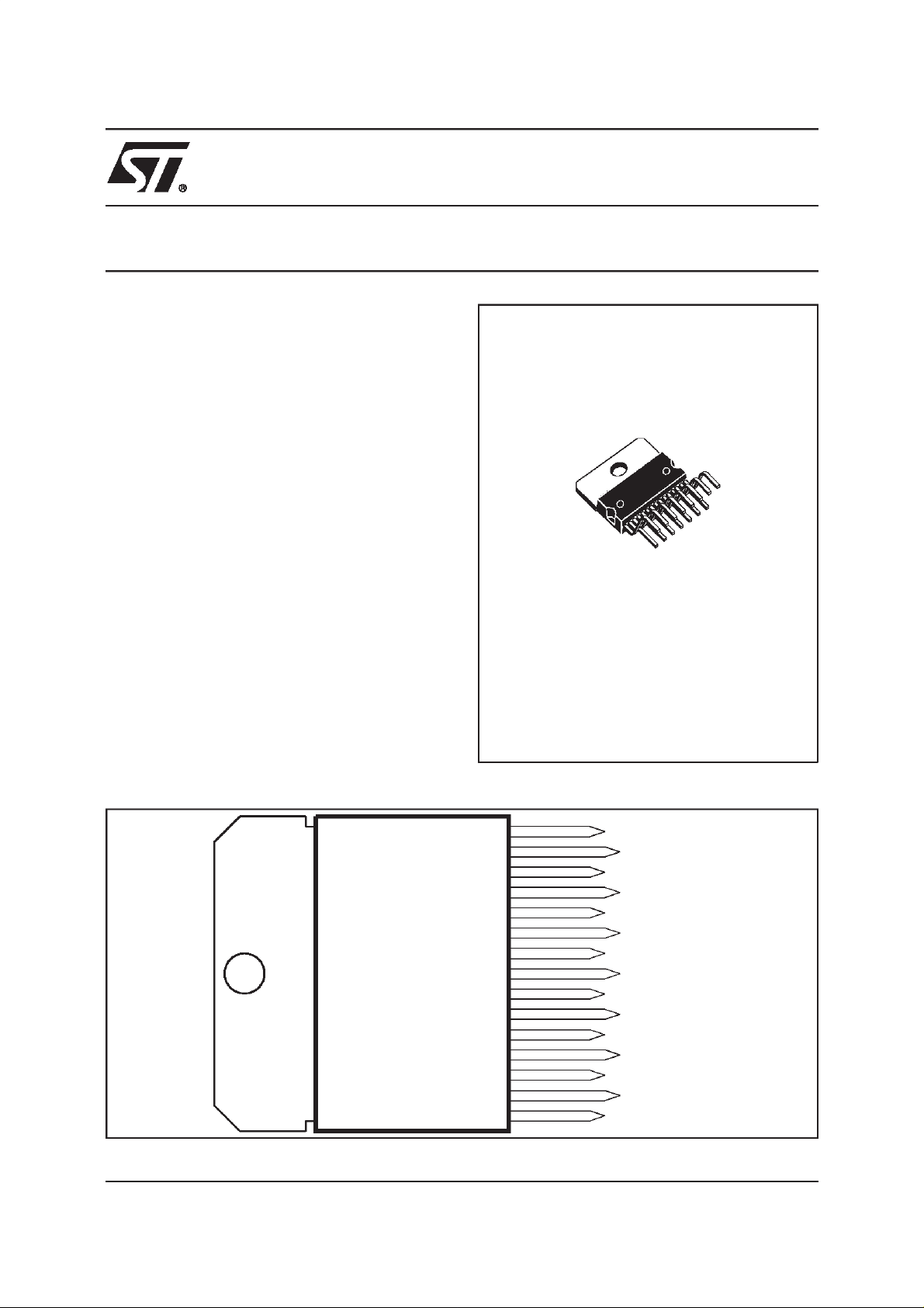
MULTIWATT15
(PlasticPackage)
ORDER CODE :
STV9306
PRELIMINARY DATA
STV9306
DESCRIPTION
2
The STV9306 is a fully I
deflection IC designed for use in 110°,4/3 or 16/9
CRT applications. It integrates both the vertical
deflection and E/W correction circuitries necessary in design of a 110°chassis.
PIN CONNECTIONS
C controlled vertical
15
14
13
12
11
10
BREATHING
SENS1
EWFB
SENS2
EWOUT
VOPS
9
8
7
6
5
4
3
2
1
OUT
GND
FLYBACK
V
S
SYNC
CHOLD
SDA
CRAMP
SCL
9306-01.EPS
December 1998
This isadvance informationon a newproductnow in developmentor undergoingevaluation. Detailsare subject to change without notice.
1/12
Page 2
STV9306
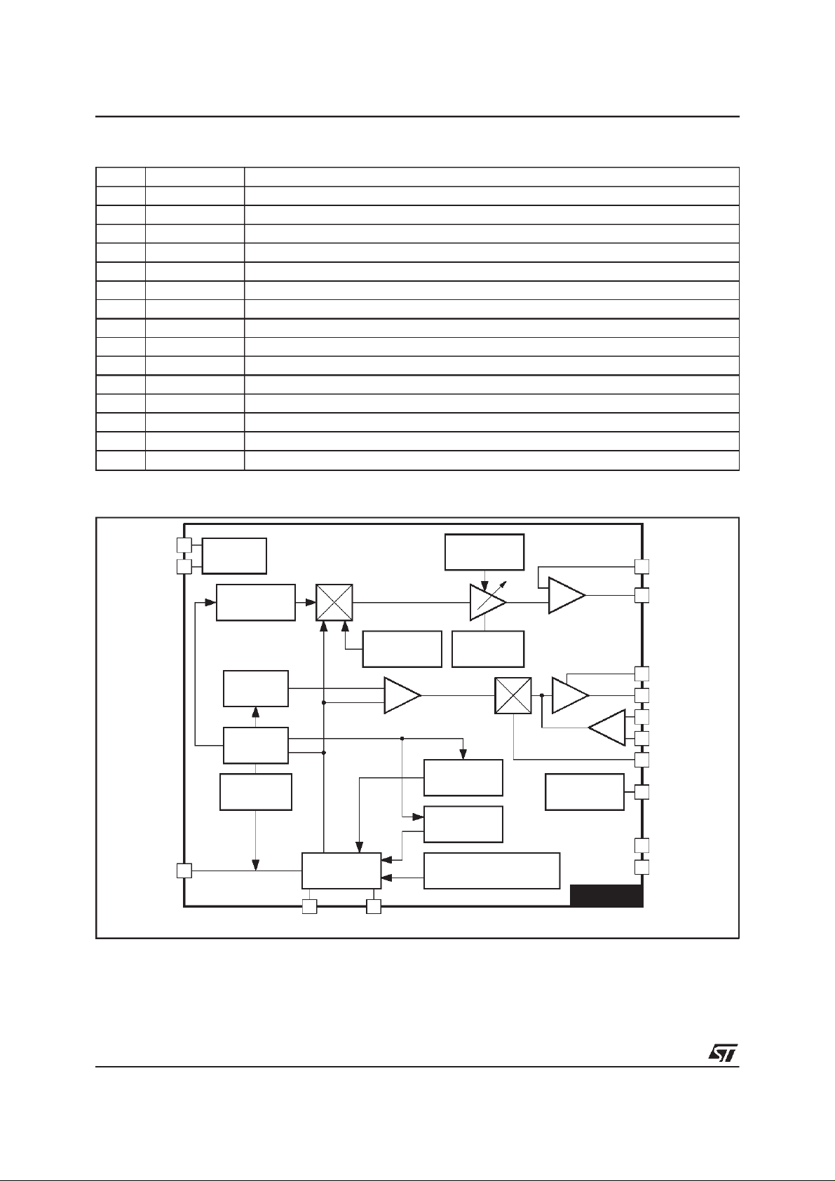
PIN LIST
Pin Symbol Description
1 SCL I
2 CRAMP Ramp Capacitor
3 SDA I
4 CHOLD Hold Capacitor
5 SYNC Sync Input
6 VS Supply Voltage
7 FLYBACK Flyback Output
8 GND Ground
9 OUT Vertical Output
10 VOPS Vertical Output Power Supply
11 EWOUT EW Output
12 SENS2 Vertical Current Sense 2
13 EWFB EW Feedback
14 SENS1 Vertical Current Sense 1
15 BREATHING Breathing Input
BLOCKDIAGRAM
2
C Bus Clock
2
C Bus Data
9306-01.TBL
SDA
SCL
SYNC +
OVERSIZE
3
1
5
BUS
DECODER
TRAPEZIUM
CORRECTION
VERTICAL
SHIFT
V MIDDLE
SCREEN
OVERSIZE
BLANKING
CORNER
CORRECTIONEWAMPLITUDE
RAMP
GENERATOR
2
CRAMP CHOLD
4
HORIZONTAL
WIDTH
C
CORRECTION
S
CORRECTION
VERTICALAMPLITUDE
ADJUSTMENT& FORMAT
FLYBACK
GENERATOR
STV9306
13
EWFB
11
EWOUT
10
VOPS
9
OUT
14
SENS 1
12
SENS 2
15
BREATHING
7
FLYBACK
8
GND
6
V
S
9306-02.EPS
2/12
Page 3
STV9306
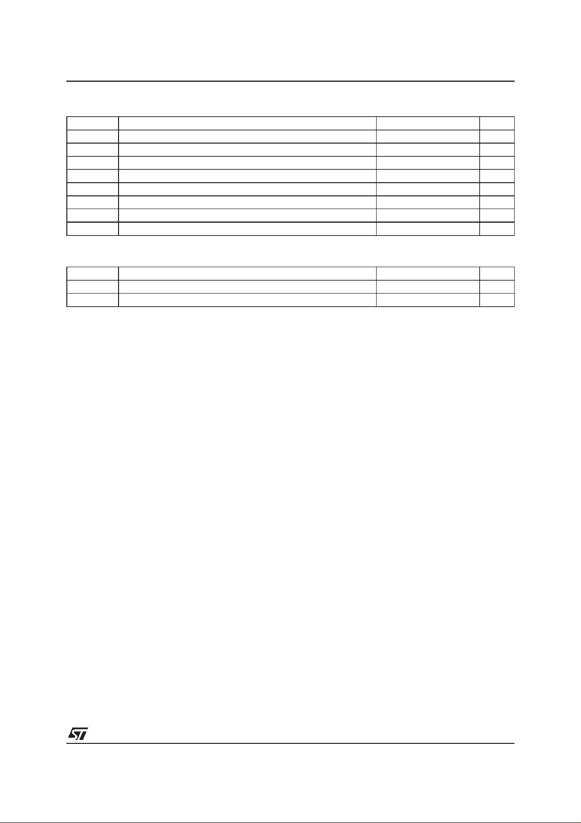
ABSOLUTE MAXIMUMRATINGS
Symbol Parameter Value Unit
V
S
V
OUT
V
V
IS
E/W OUT East/West Output 60 V
T
oper
T
stg
T
THERMALDATA
Symbol Parameter Value Unit
R
th (j-c)
T
Supply Voltage 35 V
Flyback Peak Voltage 60 V
Input Voltage at Pins 1-3-5-12-13-14-15 -0.3, V
I
Input Voltage at Pins 2-4 10 V
Operating Temperature -10, +70
Storage Temperature -55, +150
Junction Temperature +150
j
Junction-case Thermal Resistance Max. 3
Temperature for Thermal Shutdown Min. 140
t
S
o
o
o
o
C/W
o
V
C
C
C
9306-02.TBL
C
9306-03.TBL
3/12
Page 4
STV9306
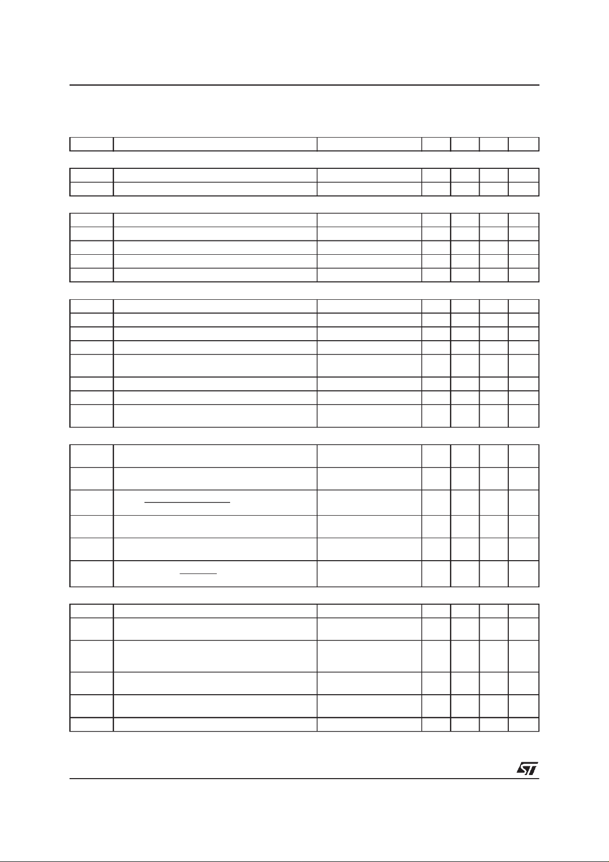
ELECTRICALCHARACTERISTICS
= 24V,R
V
S
Symbol Parameter Test Conditions Min. Typ. Max. Unit
SUPPLY
V
S
I
S
RAMP GENERATOR CONTROL
V
Rlow
t
D
I
ISY
V
THSY
I
OB
POWER AMPLIFIER
I
IBR
V
BREATH
V
7H
V
7L
I
SENS1
I
SENS2
V
9H
V
9L
/st
dV
9H
/dt
dV
9L
VERTICAL OUTPUT (Pin 9)
I
PP
I
DC
Z
SLP
I
SC
I
CC
BR
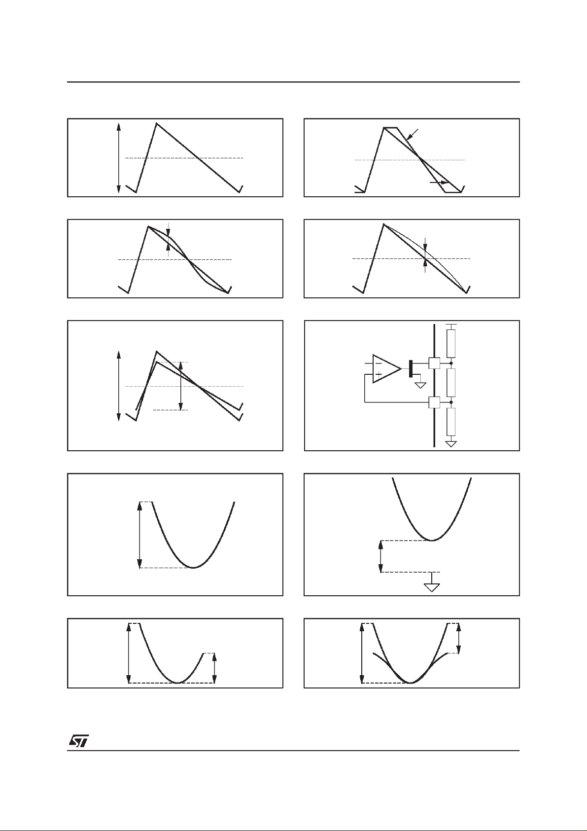
EAST/WEST CORRECTION (V_SAW = 100000, V_SH = 10000, V_SC = 0000, V_CC = 1000) (see Figure 6)
I
BIAS
V
PAR
V
DCEW
Trap Trapezium Correction at Pin 13 (see Figure 9)
Shape Parabola Shape (cornercorrection) at Pin 13
V
11L
= 0.5Ω, Normal mode, T
SENS
=25oC, unless otherwise specified
amb
Operating Supply Voltage 16 28 V
Supply Current on Pins 6-10 IO= 0 40 60 mA
Minimum V
Voltage atPin 2 1.8 2 2.2 V
RAMP
Discharge Time at Pin 2 50 µs
Synchro Input Current at Pin 5 VSY= 0 -6 -3 µA
Synchro Threshold Voltage at Pin 5 2.5 3 3.5 V
Oversize Blank Input Current at Pin 5 70 100 µA
Breathing Current Input Current at Pin 15 V
= 0V -10 -5 µA
BREATH
Breathing Operating Voltage atPin 15 0 9 V
Saturation Voltage to supply at Pin 7 IO= -1.5A, V9>VS+ 5V 2.5 3.5 V
Saturation Voltage to Ground atPin 7 IO= 100mA 1.5 2.5 V
-20
Bias Input Current at Pin 14
Bias Input Current at Pin 12
V14=0V
=0V
V
12
-20
-10
-10
Saturation Voltageto supply at Pin 9 versus Pin 10 IO= -1.5A 2.5 3.5 V
Saturation Voltage to Ground atPin 9 IO= 1.5A 1.5 2.5 V
Vertical Deflection Current (see Figure 1) V_SAW = 000000
V_SAW = 111111
Average Current (vertical shift)
at V_SAW = 111111
slope in zoom mode
Z
=
SLP
slope in normal mode
(see Figure 2)
V_SH = 01111
V_SH = 11111
V_ZOOM =000
V_ZOOM =111
S Correction = ISC/IPP(see Figure 3) V_SC = 0000
V_SC = 1111
C Correction = ICC/IPP(see Figure 4) V_CC = 0111
V_CC = 1111
I
− I
PP
Breathing BR =
PPB
I
PP
(see Figure 5)
BR
BR
Min.V15
Max.V15
=9V
=1V
+10
+5
1.8
3
-0.35
0.35
106
130
0
6
-3
3
0
10
mV/°C
mV/°C
Input Bias Current at Pin 13 -1 -0.5 µA
Parabola Amplitude (pincushion correction)
at Pin 13(see Figure 7)
Horizontal Width Adjustment at Pin 13
(see Figure 8)
Trap = V
(see Figure 10) - Shape = V
PARTUP/VPARTLOW
COR/VPAR
Saturation Voltage I
EW_AMP = 00000
EW_AMP = 11111
EW_DC = 00000
EW_DC = 11111
HShrink active
EW_TRAP = 01111
EW_TRAP = 11111
EW_SHAPE = 00000
EW_SHAPE = 11111
= 500mA 2 V
OUT
0
5
1
6
+6
0.6
1.7
0
50
µA
µA
A
A
A
A
%
%
%
%
%
%
%
%
V
V
V
V
V
%
%
9306-04.TBL
4/12
Page 5
STV9306
Figure1
Figure3
Figure5
Figure2
Zoom Mode
I
I
PP
DC
Normal Mode
9306-03.EPS
9306-04.EPS
Figure4
I
SC
I
CC
9306-05.EPS
9306-06.EPS
Figure 6
EWOUT
I
PPB
I
PP
EWSENS
11
13
Figure7
Figure9
V
V
PARUP
PAR
V
PARLOW
9306-07.EPS
Figure8
9306-09.EPS
Figure10
9306-11.EPS
9306-08.EPS
V
DCEW
9306-10.EPS
V
COR
V
PAR
9306-12.EPS
5/12
Page 6
STV9306
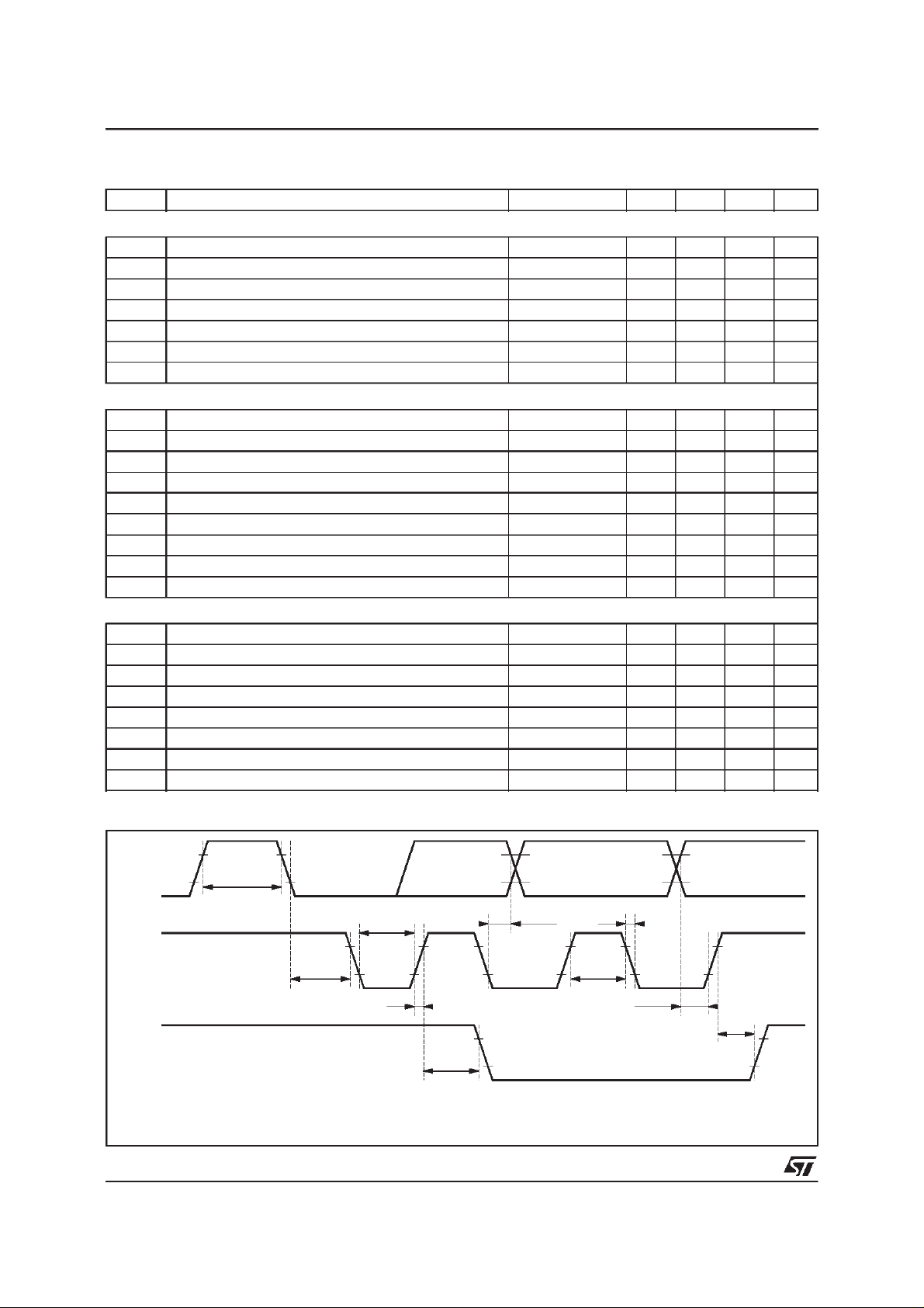
I2C BUS CHARACTERISTICS
Symbol Parameter Test Conditions Min. Typ. Max. Unit
SCL (Pin 1)
V
Low Level Input Voltage -0.3 +1.5 V
IL
High Level Input Voltage 3.0 5.5 V
V
IH
Input Leakage Current VIN= 0 to 5V -10 +10 µA
I
LI
f
SDA (Pin 3)
V
TIMING
t
t
HIGH
t
SU, DAT
t
HD, DAT
t
SU, STO
t
t
HD, STA
t
SU, STA
Clock Frequency 0 100 kHz
SCL
Input Rise Time 1.5V to 3V 1000 ns
t
R
Input Fall Time 1.5V to 3V 300 ns
t
F
Input Capacitance 10 pF
C
I
V
Low Level Input Voltage -0.3 +1.5 V
IL
High Level Input Voltage 3.0 5.5 V
V
IH
Input Leakage Current VIN= 0 to 5V -10 +10 µA
I
LI
Input Capacitance 10 pF
C
I
Input Rise Time 1.5V to 3V 1000 ns
t
R
Input Fall Time 1.5V to 3V 300 ns
t
F
Low Level Output Voltage IOL= 3mA 0.4 V
OL
Output Fall Time 3V to 1.5V 250 ns
t
F
Load Capacitance 400 pF
C
L
Clock Low Period 4.7 µs
LOW
Clock High Period 4.0 µs
Data Set-up Time 250 ns
Data Hold Time 0 340 ns
Set-up Time fromClock High to Stop 4.0 µs
Start Set-up Time following a Stop 4.7 µs
BUF
Start Hold Time 4.0 µs
Start Set-upTime following Clock Low-to HighTransition 4.7 µs
9306-05.TBL
Figure11 : I2C Bus Timing
SDA
SCL
SDA
6/12
t
BUF
t
HD,STA
t
LOW
t
HD,DAT
t
R
t
SU,STA
t
HIGH
t
F
t
SU,DAT
t
SU,STO
9306-13.EPS
Page 7
STV9306
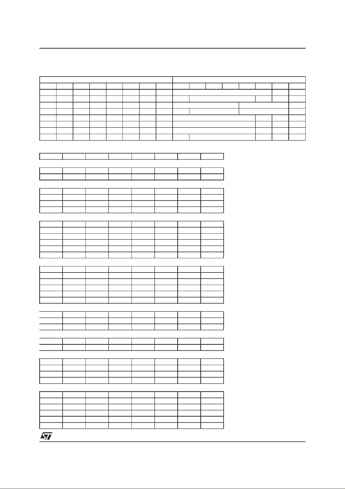
I2C SELECTION
1 - Write Mode :
B7 B6 B5 B4 B3 B2 B1 B0 B7 B6 B5 B4 B3 B2 B1 B0
000XXXX0 VERTICAL AMPLITUDE X 1
001XXXX0SIGN VERTICAL SHIFT X X 1
010XXXX0 S.CORRECTION ZOOM MODE 1
011XXXX0SIGN C. CORRECTION ZOOM AMPLITUDE 1
100XXXX0 HORIZONTAL WIDTH Hshr X 1
101XXXX0 E/WCORRECTION X X 1
110XXXX0E/WCORNER CORRECTION ext. T X 1
111XXXX0SIGN TRAP. CORRECTION Himp X 1
Data
B7 B6 B5 B4 B3 B2 B1 B0
L0 : VERTICAL AMPLITUDE (V_SAW)
0 0 0 0 0 0 X 1 Min. Amplitude
1 1 1 1 1 1 X 1 Max. Amplitude
L1 : VERTICAL SHIFT(V_SH)
X 0 0 0 0 X X 1 Min.Shift Level
X 1 1 1 1 X X 1 Max. Shift Level
1XXXXXX1Positive Shift
0XXXXXX1Negative Shift
L2 : S CORRECTION (V_SC) & ZOOM POSITION
0 0 0 0 X X X 1 Min.S Correction
1 1 1 1 X X X 1 Max. S Correction
X X X X 0 0 X 1 Normal Mode
X X X X 0 1 X 1 Unzoom
X X X X 1 X X 1 Zoom
X X X X X X 1/0 1 Subtitle(active = 1)
L3 : C CORRECTION (V_CC) & PROGRESSIVE ZOOM (V_ZOOM)
1XXXXXX1Positive C Correction
0XXXXXX1Negative C Correction
X 0 0 0 X X X 1 Min. C Correction
X 1 1 1 X X X 1 Max. C Correction
X X X X 0 0 0 1 Min. Zoom
X X X X 1 1 1 1 Max. Zoom
L4 : HORIZONTAL WIDTH ADJ (EW_VDC)
0 0 0 0 0 X X 1 Hwidth Min. Level
1 1 1 1 1 X X 1 Hwidth Max. Level
X X X X X 1/0 X 1 Hwidth Shrink (active = 1)
L5 : PINCUSHION CORRECTION (EW_AMP)
0 0 0 0 0 X X 1 Min. Amplitude
1 1 1 1 1 X X 1 Max. Amplitude
L6 : E/W SHAPE(EW_SHAPE)
0 0 0 0 0 X X 1 Min. Shape Correction
1 1 1 1 1 X X 1 Max. Shape Correction
X X X X X 1 X 1 E/W Transistor OUT
X X X X X 0 X 1 E/W Transistor IN
L7 : TRAPEZIUM CORRECTION (EW_TRAP) & HIGH IMPEDANCE
1XXXXXX1Positive Trapezium Correction
0XXXXXX1Negative Trapezium Correction
X 0 0 0 0 X X 1 Min. Level Correction
X 1 1 1 1 X X 1 Max. Level Correction
X X X X X 0 X 1 Normal Mode
X X X X X 1 X 1 High Impedance
SlaveAddress: 1000 1100(8C)
Subaddress Data
7/12
Page 8
STV9306
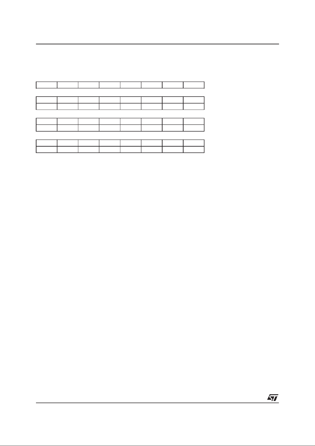
I2C SELECTION(continued)
2 - Read Mode :
Data
B7 B6 B5 B4 B3 B2 B1 B0
THERMAL SECURITY STATUS
0XXXXXX1Normal Temperature
1XXXXXX1Thermal Security Active
FLYBACK PULSE DETECTION STATUS
X0XXXXX1Flyback Pulse detected
X1XXXXX1Lack of Flyback Pulse
SYNC PULSE DETECTION STATUS
XX0XXXX1Synchro Pulse Present
XX1XXXX1Lack of Synchro Pulse
Slave Address: 1000 1101(8D)
8/12
Page 9
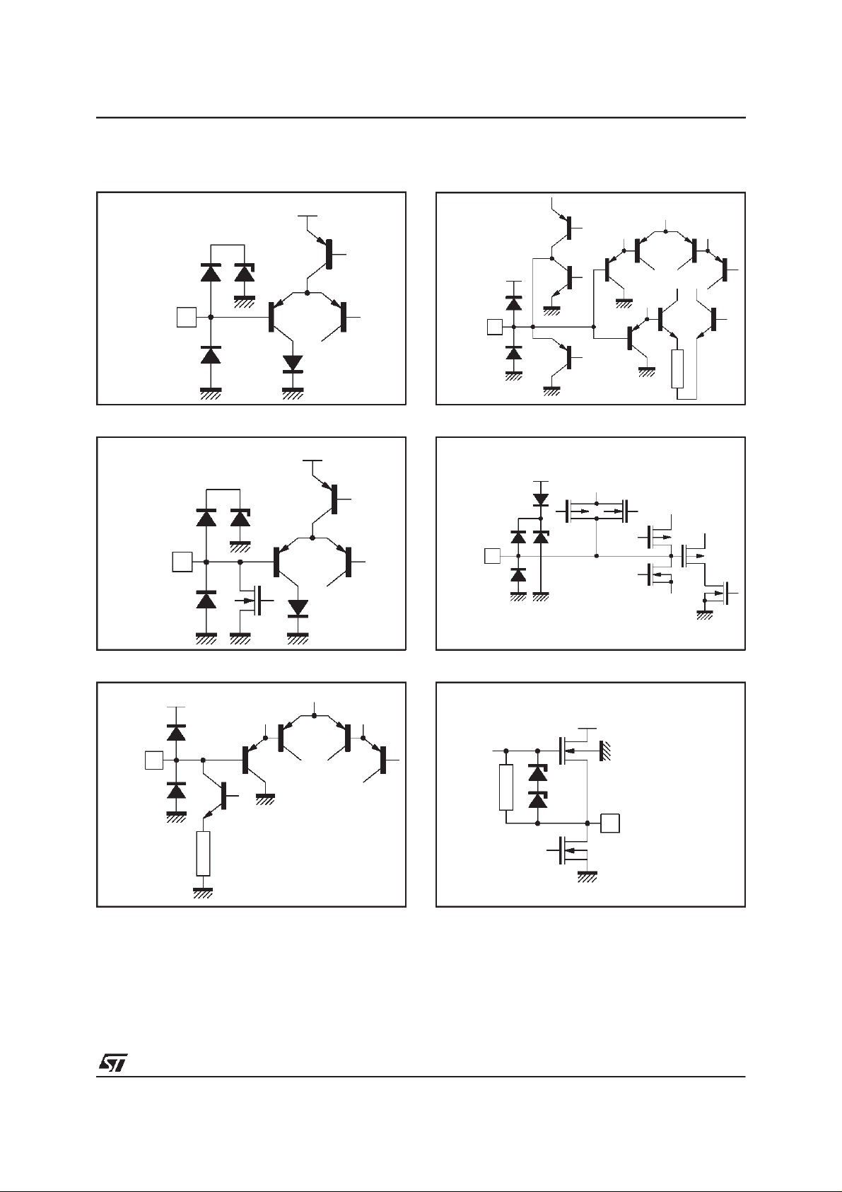
INPUT/OUTPUTPIN CONFIGURATION
Figure12
5V
STV9306
Figure13
SCL
Figure14
SDA
Figure16
Clamp
30V
1
CRAMP
9306-14.EPS
V
S
2
9306-15.EPS
Figure15
5V
5V
Clamp
30V
3
9306-16.EPS
4CHOLD
9306-17.EPS
Figure17
SYNC
V
S
V
OPS
5
7
FLYBACK
9306-18.EPS
9306-19.EPS
9/12
Page 10
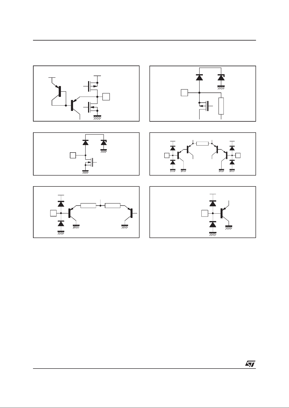
STV9306
INPUT/OUTPUTPIN CONFIGURATION (continued)
Figure18
V
V
S
OPS
Figure19
Clamp
60V
Figure20
Figure22
EWFB
13
OUT
VOPS
9
9306-20.EPS
10
9306-21.EPS
Figure21
V
Clamp
S
60V
11EWOUT
9306-22.EPS
12 14SENS2 SENS1
V
S
9306-23.EPS
Figure23
15
V
S
V
S
BREATHING
10/12
9306-24.EPS
9306-25.EPS
Page 11
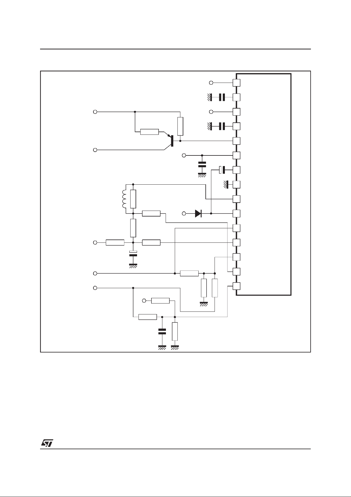
APPLICATIONSCHEMATIC
STV9306
VSYNC
OVERSIZE
BLANKING
12V
EW DIODE
MODULATOR
BCL
V. YOKE
R =9.6Ω
L = 27mH
I = 1.3A
PP
560Ω
470Ω
100Ω
1Ω
100Ω10Ω
1000µF
12V
BC557
220kΩ
24V
24V
Ω
10k
1N4004
10kΩ
SCL
SDA
100nF
2.2kΩ
100nF
330nF
100µF
15kΩ
1
2
3
4
5
6
7
8
9
10
11
12
13
14
15
SCL
CRAMP
SDA
CHOLD
SYNC
V
S
FLYBACK
GND
OUT
VOPS
EWOUT
SENS2
EWFB
SENS1
BREATH
S
T
V
9
3
0
6
100kΩ
1nF
Ω
68k
9306-26.EPS
11/12
Page 12
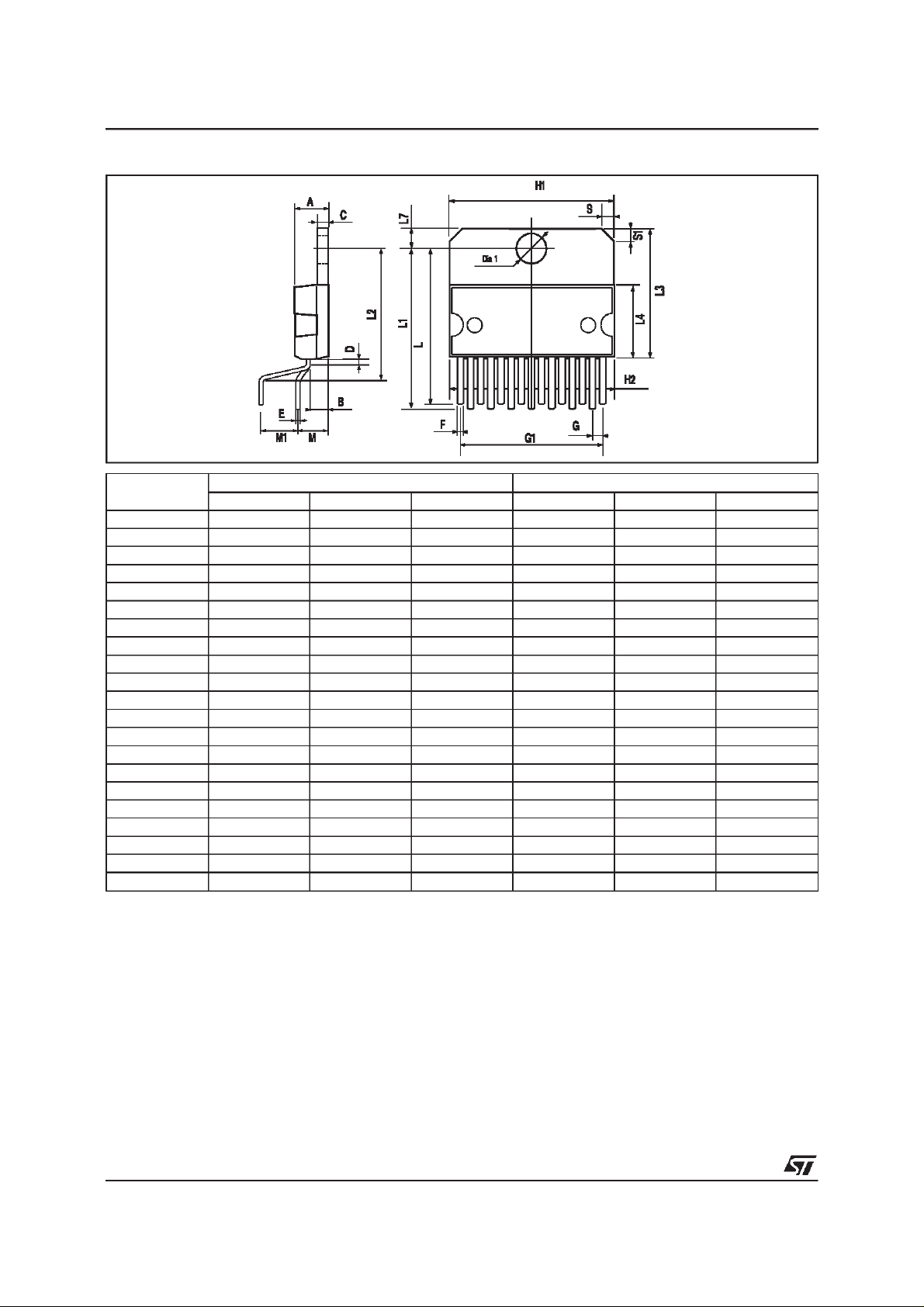
STV9306
PACKAGE MECHANICAL DATA:
Dimensions
Min. Typ. Max. Min. Typ. Max.
15 PINS - PLASTICMULTIWATT
Millimeters Inches
A 5 0.197
B 2.65 0.104
C 1.6 0.063
D 1 0.039
E 0.49 0.55 0.019 0.022
F 0.66 0.75 0.026 0.030
G 1.02 1.27 1.52 0.040 0.050 0.060
G1 17.53 17.78 18.03 0.690 0.700 0.710
H1 19.6 0.772
H2 20.2 0.795
L 21.9 22.2 22.5 0.862 0.874 0.886
L1 21.7 22.1 22.5 0.854 0.870 0.886
L2 17.65 18.1 0.695 0.713
L3 17.25 17.5 17.75 0.679 0.689 0.699
L4 10.3 10.7 10.9 0.406 0.421 0.429
L7 2.65 2.9 0.104 0.114
M 4.25 4.55 4.85 0.167 0.179 0.191
M1 4.63 5.08 5.53 0.182 0.200 0.218
S 1.9 2.6 0.075 0.102
S1 1.9 2.6 0.075 0.102
Dia. 1 3.65 3.85 0.144 0.152
Information furnished is believed to be accurate and reliable. However, STMicroelectronics assumes no responsibility for the
consequences of use of such information nor for any infringement of patents or other rights of third parties which may result from
its use. No licence is granted by implication or otherwise under any patent or patent rights of STMicroelectronics. Specifications
mentioned in this publication are subject to change without notice. This publication supersedes and replaces all information
previouslysupplied.STMicroelectronicsproducts are not authorizedfor use ascriticalcomp onentsin lifesupport devicesor systems
without express written approval of STMicroelectronics.
Purchase of I
Rights to use these components in a I
Australia - Brazil- Canada - China - France - Germany - Italy - Japan - Korea - Malaysia - Malta - Mexico - Morocco - The Netherlands
Singapore - Spain- Sweden - Switzerland- Taiwan - Thailand - United Kingdom - U.S.A.
The ST logo is a registered trademark of STMicroelectronics
1998 STMicroelectronics - All Rights Reserved
2
C Components of STMicroelectronics, conveys a licenseunder the PhilipsI2C Patent.
2
C Standard Specifications as defined by Philips.
the I
STMicroelectronics GROUP OF COMPANIES
2
C system, is granted provided that the system conforms to
http://www.st.com
12/12
PM-MW15V.EPS
MW15V.TBL
 Loading...