

Page 1
STV7733
AOC1
DBA1
DBA2
DIR /CS SCLK VDD
/DL
VSSL
DBB1
DBB2
DBC1
DBC2
AOC2
HVDD
STBTEST
OUT1 OUT2 OUT320
MVDD
2 x 320-bit latch
Q1 Q2 Q3 Q4 Q320
Output control
Tri-level output buffer stage
DBD1
DBD2
Shift register direction
2 x 80-bit shift register
VSSP
HVDD
MVDD
VSSP
Data decoding
POE
VSSS
2 x 80-bit shift register
2 x 80-bit shift register
2 x 80-bit shift register
OE
320 output dot-matrix display driver
Preliminary Data
Features
■
High-voltage, row/column driver IC
■
320, tri-level (high-voltage, medium voltage
and ground) power outputs:
– capable of operating at 90V, absolute max.
– capable of sinking or sourcing 2mA
– Hi-Z
■
Logic supply range: 2.5V to 3.3V
■
Slim shape die for COG, COF and TCP
solutions
■
Interface:
– four dual (2-bit) input serial buses:
DBA[1:2], DBB[1:2], DBC[1:2] and DBD[1:2]
operating at shift clock frequency of
10MHz, max.
– three control inputs: shift clock direction
(DIR), chip select (/CS) and data latch
(/DL)
– two “all output” stage control inputs: AOC1
and AOC2
■
Power supplies:
– high-voltage for power outputs: 90V, max.
– logic supply suitable for battery powered
applications: 2.5V, min.
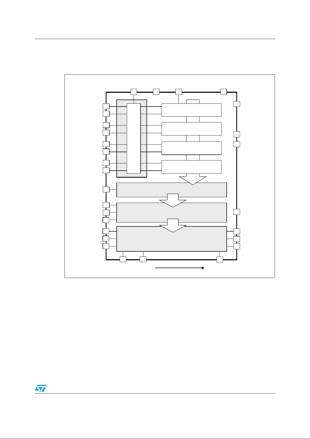
The STV7733 communicates with the host
controller through an 8-bit parallel interface. The
input data bus is organized as four, 2 x 80-bit shift
registers operating in parallel at a maximum clock
frequency of 10MHz.
Logic inputs are LVCMOS compatible.
The STV7733 is available in bumped die form.
Bumped die can be assembled in either a TCP or
COG module.
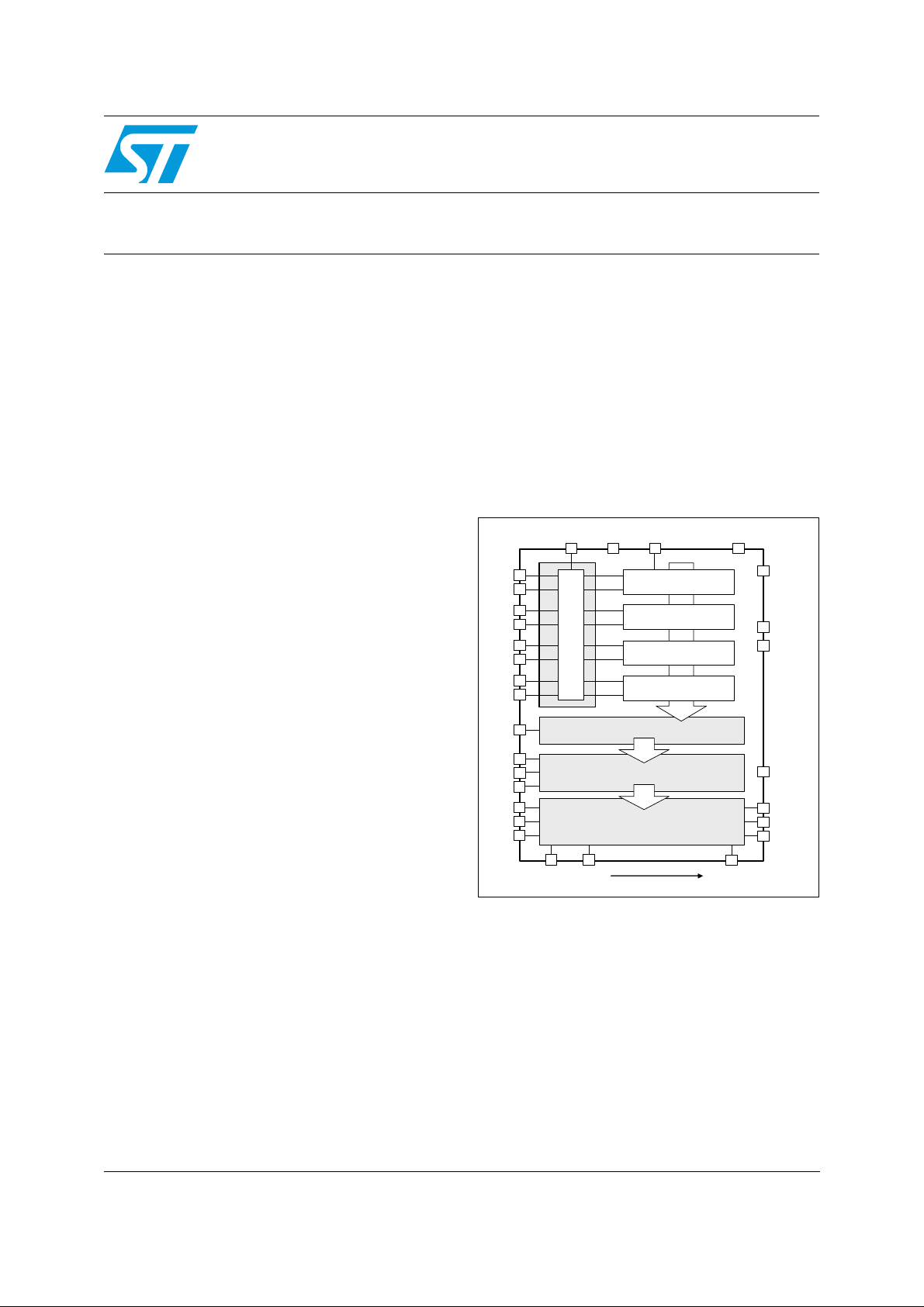
Figure 1. Block diagram
Description
The STV7733 device is a low-power,
controller/driver IC for dot-matrix displays. Data is
encoded on two bits to select one of four possible
output states: high level, medium level, ground or
high impedance (Hi-Z).
Inputs AOC1 and AOC2 control the all output
stages simultaneously to select one of five
possible configurations: high level, medium level,
ground, Hi-Z or data through.
Except for the data through mode, the
configuration selected by AOC1 and AOC2 is
applied to all outputs at the same time.
May 2007 Rev 1 1/28
This is preliminary information on a new product now in development or undergoing evaluation. Details are subject to
change without notice.
www.st.com
28
Page 2

Contents STV7733
Contents
1 Block diagram . . . . . . . . . . . . . . . . . . . . . . . . . . . . . . . . . . . . . . . . . . . . . . 3
2 Pin description . . . . . . . . . . . . . . . . . . . . . . . . . . . . . . . . . . . . . . . . . . . . . 4
3 Die pinout . . . . . . . . . . . . . . . . . . . . . . . . . . . . . . . . . . . . . . . . . . . . . . . . . . 5
4 Data bus configuration . . . . . . . . . . . . . . . . . . . . . . . . . . . . . . . . . . . . . . . 6
5 Power output stage . . . . . . . . . . . . . . . . . . . . . . . . . . . . . . . . . . . . . . . . . . 7
6 Absolute maximum ratings . . . . . . . . . . . . . . . . . . . . . . . . . . . . . . . . . . . 8
7 Electrical characteristics . . . . . . . . . . . . . . . . . . . . . . . . . . . . . . . . . . . . . 9
8 AC timing requirements . . . . . . . . . . . . . . . . . . . . . . . . . . . . . . . . . . . . . 11
9 AC Timing characteristics . . . . . . . . . . . . . . . . . . . . . . . . . . . . . . . . . . . 12
10 Timing . . . . . . . . . . . . . . . . . . . . . . . . . . . . . . . . . . . . . . . . . . . . . . . . . . . . 13
11 Pad dimensions (in microns)/pad positions . . . . . . . . . . . . . . . . . . . . 14
12 Ordering information . . . . . . . . . . . . . . . . . . . . . . . . . . . . . . . . . . . . . . . 27
13 Revision history . . . . . . . . . . . . . . . . . . . . . . . . . . . . . . . . . . . . . . . . . . . 27
2/28
Page 3
STV7733 Block diagram
AOC1
DBA1
DBA2
DIR /CS SCLK VDD
/DL
VSSL
DBB1
DBB2
DBC1
DBC2
AOC2
HVDD
STBTEST
OUT1 OUT2 OUT320
MVDD
2 x 320-bit latch
Q1 Q2 Q3 Q4 Q320
Output control
Tri-level output buffer stage
DBD1
DBD2
Shift register direction
2 x 80-bit shift register
VSSP
HVDD
MVDD
VSSP
Data decoding
POE
VSSS
2 x 80-bit shift register
2 x 80-bit shift register
2 x 80-bit shift register
OE
1 Block diagram
Figure 2. STV7733 block diagram
3/28
Page 4
Pin description STV7733
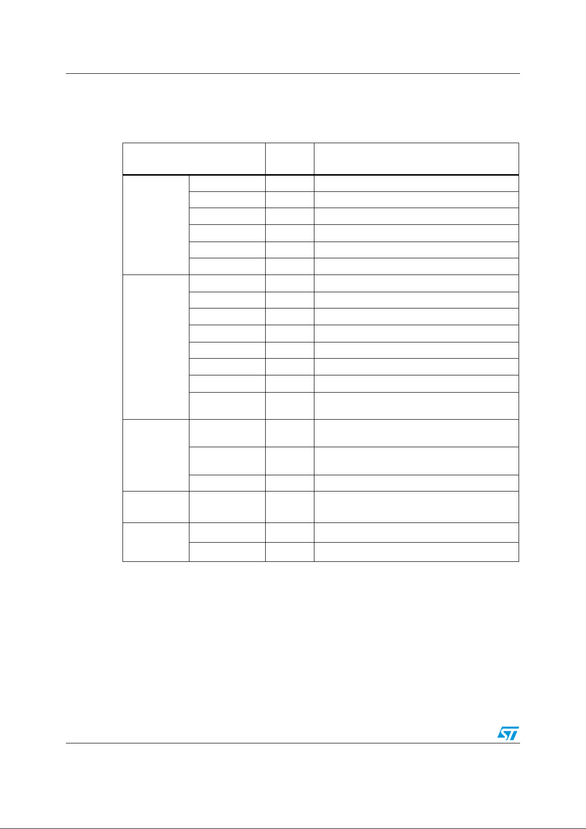
2 Pin description
Table 1. STV7733 pin description
Pin name
Power
supplies
Input logic
block
Power output
control
Pin type
(I/O)
HVDD I Output buffer - high-voltage supply
MVDD I Output buffer - medium voltage supply
VSSP I Output buffer - ground level
VDD I Logic power supply
VSSL I Logic ground
VSSS I Chip substrate level
DBA[1:2] I Input data bus, 2-bit serial interface
DBB[1:2] I Input data bus, 2-bit serial interface
DBC[1:2] I Input data bus, 2-bit serial interface
DBD[1:2] I Input data bus, 2-bit serial interface
SCLK I Data shift clock
DIR I Shift clock direction
/CS I Chip select (0 = select, 1 = un-select)
/DL I
AOC1 I
AOC2 I
POE I Power output enable
Data latch. Shift register data is transferred to the
driver outputs at the falling edge of this pulse.
“All-output” control (all HVDD, all MVDD, all VSSP,
data through mode) selection pin
“All-output” control (all HVDD, all MVDD, all VSSP,
data through mode) selection pin
Pin description
Power
outputs
Test
4/28
OUT1to OUT320 O High-voltage power outputs
STBTEST I Must be grounded
OE I Must be grounded
Page 5
STV7733 Die pinout
Y
X
0/0
DUMMY
DUMMY
DUMMY
DUMMY
DUMMY
DUMMY
DUMMY
DUMMY
DUMMY
DUMMY
DUMMY
VDD
VSSS
VSSL
OE
DBD2
DBD1
DBC2
DBC1
DUMMY
DUMMY
DUMMY
DUMMY
DBB2
DBB1
DBA2
DBA1
VDD
VSSS
VSSL
CS
SCLK
DL
VSSL
VSSS
VDD
AOC2
AOC1
DUMMY
DUMMY
POE
DIR
STBTEST
VSSL
VSSS
VDD
DUMMY
DUMMY
DUMMY
DUMMY
DUMMY
DUMMY
DUMMY
DUMMY
DUMMY
DUMMY
DUMMY
DUMMY
OUT1
OUT2
OUT3
OUT4
OUT5
OUT316
OUT317
OUT318
OUT319
OUT320
VSSP
VSSP
HVDD
HVDD
MVDD
MVDD
VSSL
VSSS
VDD
DUMMY
DUMMY
DUMMY
DUMMY
VSSP
VSSP
HVDD
HVDD
MVDD
MVDD
VSSL
VSSS
VDD
DUMMY
DUMMY
DUMMY
DUMMY
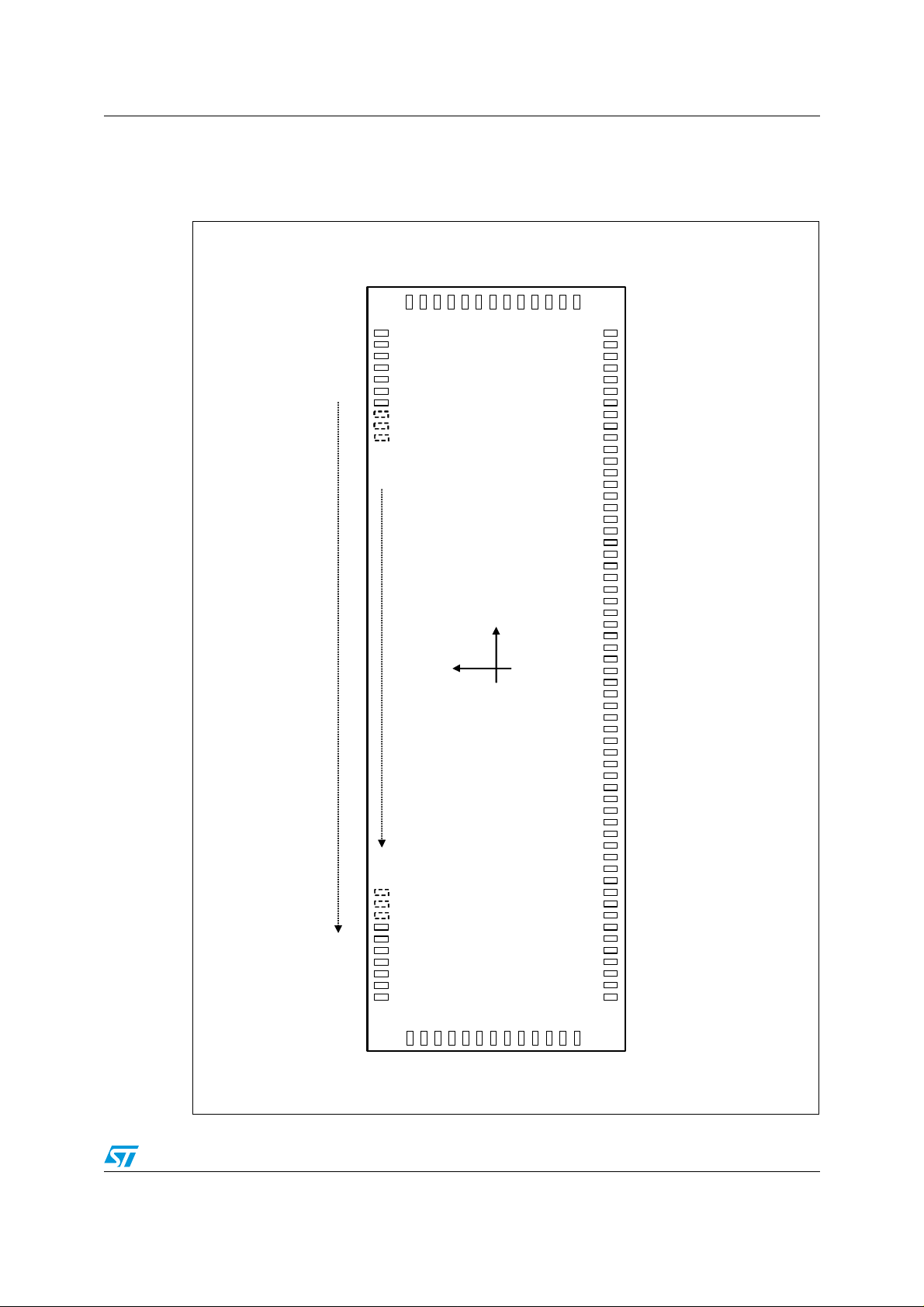
3 Die pinout
Figure 3. Die pinout
5/28
Page 6
Data bus configuration STV7733
4 Data bus configuration
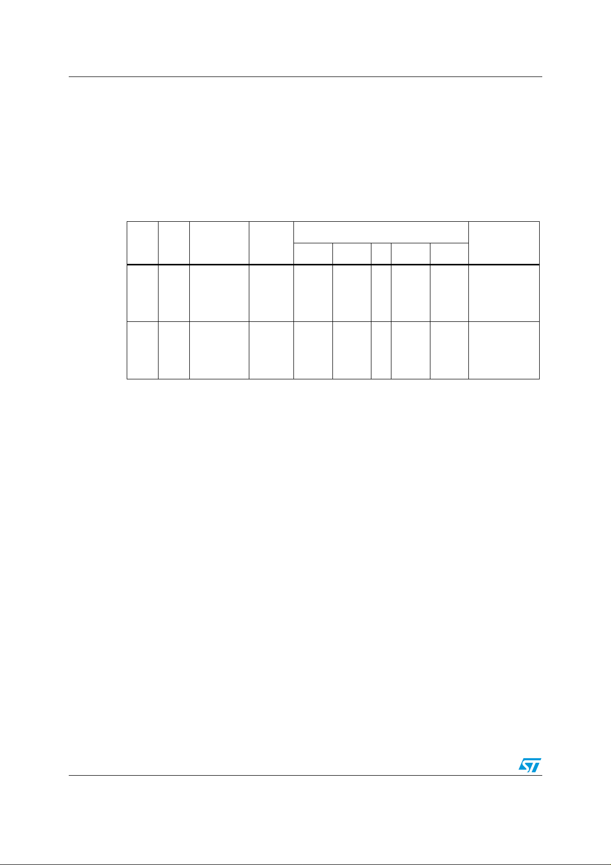
Below, Table 2 describes the position of the first data sampled by the first rising edge of the
SCLK clock. For the first configuration described in Table 2, that is, with input DIR = “H”,
data on the 2-bit bus DBA is sampled by the first SCLK clock pulse and appears on power
output OUT1. After 80 clock pulses, data on OUT1 will be shifted to OUT317 - on the
high-to-low transition of input /DL. Input /CS is the chip select.
Table 2. Data bus configuration
SCLK pulse number
/CS DIR Input Position
OUT1 OUT2 … OUT79 OUT80
Comment
L H
L L
DBA[1:2]
DBB[1:2]
DBC[1:2]
DBD[1:2]
DBA[1:2]
DBB[1:2]
DBC[1:2]
DBD[1:2]
OUT
OUT
OUT
OUT
OUT
OUT
OUT
OUT
01
02
03
04
320
319
318
317
05
06
07
08
316
315
314
313
313
314
315
316
08
07
06
05
317
318
319
320
04
03
02
01
Left/Right shift
Right/Left shift
Note: Data is transferred from the shift register to a latch block and then on to power output stages
on the falling edge of input /DL, see Figure 2.
All output data is stored and held in the latch block on the rising edge of the input /DL, see
Figure 2.
6/28
Page 7
STV7733 Power output stage
5 Power output stage
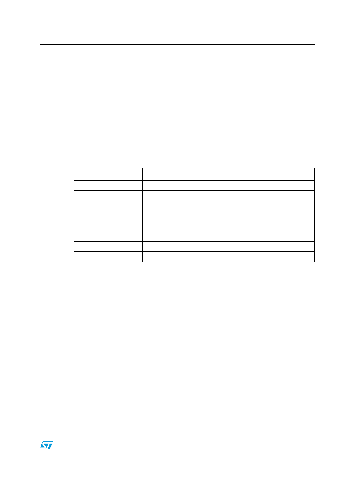
The power output stage is defined by a set of three switches that can select three different
output voltages (HVDD, MVDD or V
the output stage in a high impedance (Hi-Z) mode.
Depending on the configuration of logic inputs AOC1 and AOC2, the power output stage is
configured in either a “data through” mode or a “simultaneous” mode. In the “data through”
mode (for AOC1 = AOC2 = “L”), the power output stage converts the 2-bit encoded data that
was loaded into the latch stage for each column into a high-voltage level that appears on the
output pin. When AOC1 and AOC2 are not both “L”, the power outputs can all operate
simultaneously - going to V
, MVDD or HVDD depending on AOC1 and AOC2 as described
SSP
below in Table 3.
Table 3. Power output truth table
DBn[1] DBn[2] POE AOC1 AOC2 OUTn Comment
X X L X X All Hi-Z
L L H L L Hi-Z
H L H L L V
H H H L L MV
L H H L L HV
X X H H L All V
X X H L H All MV
X X H H H All HV
1. With input POE = “L”, all power outputs are not active, that is, they are all in Hi-Z.
2. Data through mode: each power output depends on the DBn[1:2] value at the falling edge of input /DL.
3. Output simultaneous mode: all power outputs depend on the “H”/”L” input values for AOC1 and AOC2.
). These switches can also be all opened to configure
SSP
SSP
DD
DD
SSP
DD
DD
(1)
(2)
(2)
(2)
(2)
(3)
(3)
(3)
7/28
Page 8
Absolute maximum ratings STV7733
6 Absolute maximum ratings
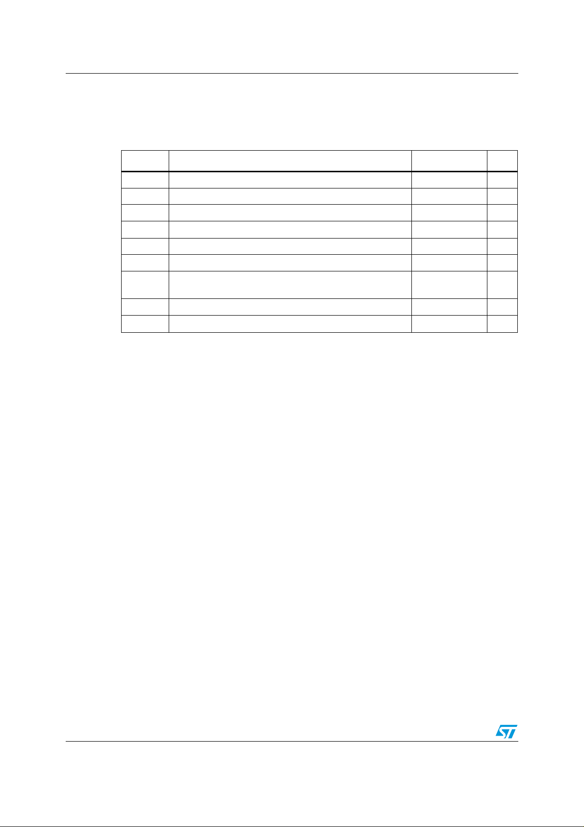
Table 4. Absolute maximum ratings
Symbol Parameter Value Units
V
HV
MV
V
I
POUT
V
OUT
V
ESD
Logic supply range -0.3, +7 V
DD
Driver supply range -0.3, +90 V
DD
Driver supply range -0.3, +HVdd -10 V
DD
Logic input voltage range -0.3, VDD+0.3 V
IN
Driver output current ±5 mA
Power output voltage range -0.3, +90 V
ESD susceptibility, Human Body model
(100pF discharged through 1.5kohms)
2.0 kV
Tjmax Maximum junction temperature 100 °C
Tstg Storage temperature range -50, +150 °C
8/28
Page 9
STV7733 Electrical characteristics
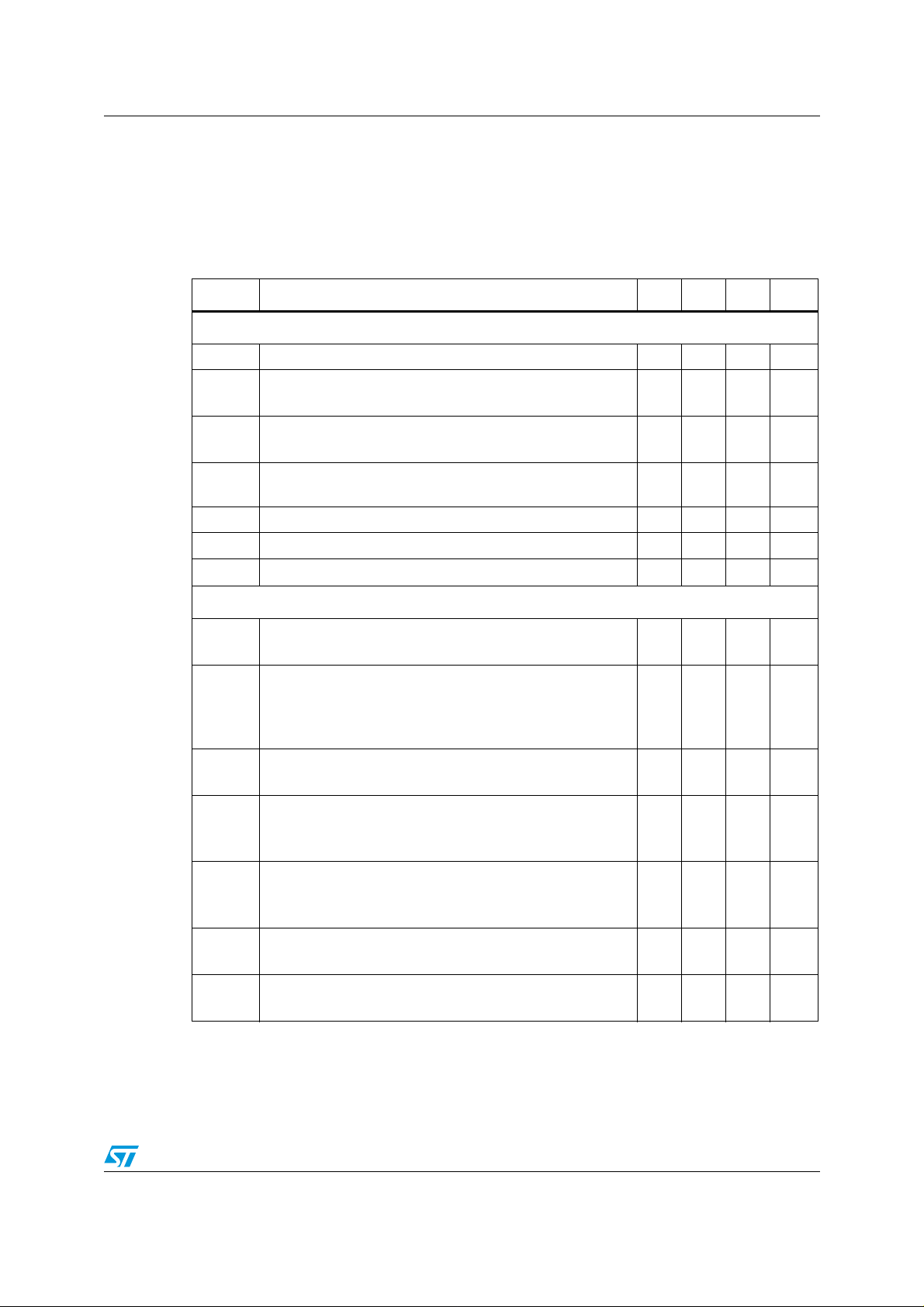
7 Electrical characteristics
VDD = 3V, HVDD = 70V, MVDD = 35V, V
SSP
= 0V, V
SSL
= 0V, V
SSS
= 0V, T
amb
= 25°C,
F = 10MHz, unless otherwise specified.
Table 5. Electrical characteristics
Symbol Parameter Min. Typ. Max. Units
Supply
V
I
I
DD1
I
DD2
HV
MV
I
OUT1 to OUT320
V
HPOUTH
V
MPOUTH
V
POUTL
I
POUTH
VDD supply voltage 2.5 3 3.3 V
DD
VDD supply current with no clock, all logic inputs set to either
DD
0V or VDD and all power outputs in Hi-Z
- - 0.5 µA
VDD dynamic supply current @ clock frequency = 5MHz
(data frequency is 2.5MHz)
VDD dynamic supply current @ clock frequency = 100kHz
(data frequency = 50kHz
HVDD supply voltage 15 80 V
DD
MVDD supply voltage
DD
HVDD supply current in steady state - - 10 µA
PP
(1)
(2)
- 3 - mA
- 0.1 - mA
15 70 V
Power output high level (voltage difference versus HVDD)
@ I
HPOUTH
= -0.5mA and HV
= 80V - - -10 V
DD
Power output medium level (voltage difference versus
MVDD)
@ I
MPOUTH
@ I
MPOUTL
= + 0.5mA and MV
= - 0.5mA and MV
DD
DD
= 40V
= 40V
-
-
--+10
Power output low level
@ I
= + 0.5mA - - +10 V
POUTL
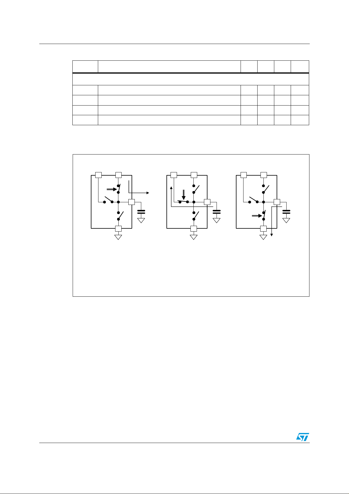
Output current from HVDD, MVDD (see Figure 4)
1) HVDD = 80V, MVDD = 40V
2) HVDD = 60V, MVDD = 30V
-1.42
-0.7
-10
- mA
V
V
mA
I
POUTM
I
POUTL
I
HiZ
Output current from output to MVDD (Figure 4)
1) HVDD = 80V and MVDD = 40V
2) HVDD = 60V and MVDD = 30V
Output current from output to V
@ Vdd=2.5V (Figure 4)
SSP
1) HVDD = 80V and MVDD = 40V
Output current during Hi-Z mode
@ V
= 2.5V, HVDD = 80V and MVDD = 40V
DD
9/28
+1.5
+0.7
mA
mA
+1.5 - mA
- 10 µA
Page 10
Electrical characteristics STV7733
Out
Cp
I
POUTH (-)
S1
S3
MV
DD HVDD
V
SSP
S2
Out
Cp
S1
S3
MV
DD HVDD
V
SSP
S2
I
POUTM (+)
Out
Cp
S1
S3
MV
DD HVDD
V
SSP
S2
I
POUTL (+)
a) I
POUTH
b) I
POUTM
c) I
POUTL
Reminder:
•
Current going into the device is a “sinking” current, considered as “positive”
•
Current coming out of the device is a “sourcing” current, considered as “negative”
Table 5. Electrical characteristics (continued)
Symbol Parameter Min. Typ. Max. Units
SCLK, DIR, /CS, DBn[1:2], /DL, AOC1, AOC2 and POE
V
V
1. This measurement is performed during device evaluation - it is not tested on all devices.
2. HVDD must be greater than MVDD under all conditions.
High level input voltage (% of VDD) 70 - - %
IH
Low level input voltage (% of VDD) - - 30 %
IL
I
High level input current @ V
IH
I
Low level input current @ V
IL
> 0.7 × V
IH
= 0V - - 5 µA
IL
DD
- - 5 µA
Figure 4. Sink/source current capability test of power outputs
10/28
Page 11
STV7733 AC timing requirements
8 AC timing requirements
VDD = 2.5V to 3.3V, T
= - 20°C to +70°C,
amb
input signal edge maximum rise and fall times (tr, tf) = 5ns.
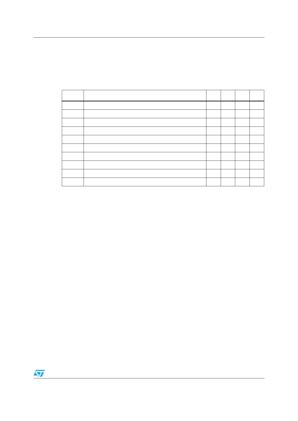
Table 6. AC timing requirements
Symbol Parameter Min. Typ. Max. Units
t
SCLK
t
WHSCLK
t
WLSCLK
t
SDAT
t
HDAT
t
SCS
t
HCS
t
HDL
t
t
SDL
Data clock period 100 - - ns
Clock pulse duration at high level 40 - - ns
Clock pulse duration at low level 40 - - ns
Input data set-up time before low-to-high clock transition 25 - - ns
Input data hold-time after low-to-high clock transition 25 - - ns
/CS set-up time before low-to-high clock transition 40 - - ns
/CS hold-time after low-to-high clock transition 25 - - ns
/DL hold-time after low-to-high transition of /CS 25 - - ns
Low level pulse duration 25 - - ns
DL
/DL set-up time before low-to-high transition of /CS 475 ns
11/28
Page 12
AC Timing characteristics STV7733
9 AC Timing characteristics
V
= 3V, HVDD = 70V, MVDD = 35V, V
DD
F = 5MHz, C
= 10pF, unless otherwise specified (V
load
VDD).
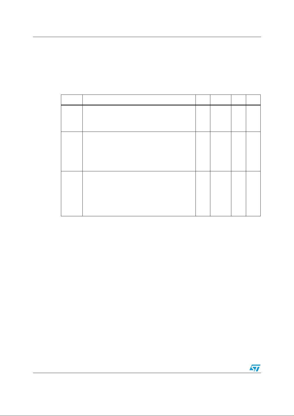
Table 7. AC timing characteristics
Symbol Parameter Min. Typ. Max. Units
Delay between /DL transition and change in level of
t
PHL2
t
PLH2
power output @ VDD = 3V (see Figure 5)
1. OUT1 and OUT320
2. OUT160 and OUT161
SSP
= 0V, V
SSL
= 0V, V
ILMAX
SSS
= 0.3 × VDD, V
= 0V, T
-
-
150
500
amb
IHMIN
= 25°C,
= 0.7 ×
250
850nsns
t
PLH3M
t
PLH3H
t
PHL3M
t
PHL3L
t
R_OUTM
t
R_OUTH
t
F_OUTM
t
F_OUTL
Delay between AOC
transitions and change in level of
1,2
power output (see Figure 5)
1. OUT1 and OUT320
2. OUT160 and OUT161
Output transition time for one single power output with
VDD = 3V, MVDD = 35V and HVDD = 70V (see
Figure 5)
Output rise time from V
Output rise time from MVDD to HV
Output fall time from HVDD to MV
Output fall time from MVDD to V
SSP
to MV
DD
DD
DD
SSP
-
-
-
-
-
-
150
500
400
500
800
200
250
850nsns
ns
ns
ns
ns
12/28
Page 13
t
WHSCLK
50%
SCLK
DB (input)
/DL
(Latch on falling edge)
50%
50%
t
WLSCLK
50%
50%
t
SDAT
t
HDAT
50%
Input timing
Output timing
OUT(n
)
90%
50%
t
DL
t
PHL2
t
SCLK
50%
/CS
t
SCS
50%
t
HCS
t
SDL
t
HDL
10%
t
PLH2
3-Steps output timing
50%
5%
55%
45%
95%
t
R_OUTM
t
R_OUTH
5%
55%
45%
95%
t
F_OUTM
50%
t
PLH3M
t
PLH3H
t
PHL3M
t
F_OUTL
t
PHL3L
HV
DD
MV
DD
V
SSP
50% 50%
AOC
1,2
OUT(n)
t
WHSCLK
50%
SCLK
DB (input)
/DL
(Latch on falling edge)
50%
50%
t
WLSCLK
50%
50%
t
SDAT
t
HDAT
50%
Input timing
Output timing
OUT(n
)
90%
50%
t
DL
t
PHL2
t
SCLK
50%
/CS
t
SCS
50%
t
HCS
t
SDL
t
HDL
10%
t
PLH2
3-Steps output timing
50%
5%
55%
45%
95%
t
R_OUTM
t
R_OUTH
5%
55%
45%
95%
t
F_OUTM
50%
t
PLH3M
t
PLH3H
t
PHL3M
t
F_OUTL
t
PHL3L
HV
DD
MV
DD
V
SSP
50% 50%
AOC
1,2
OUT(n)
STV7733 Timing
10 Timing
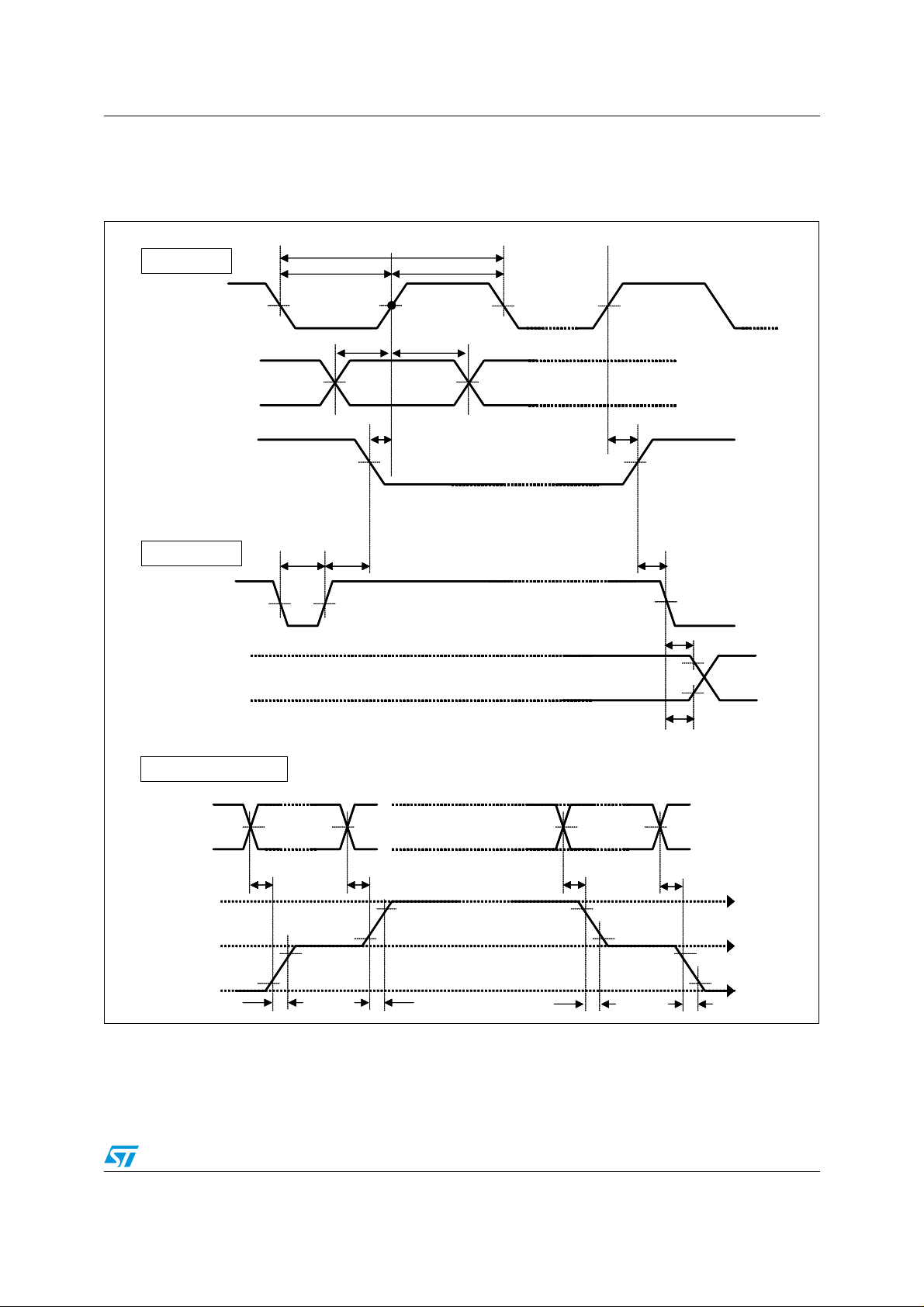
Figure 5. Timing diagram
13/28
Page 14
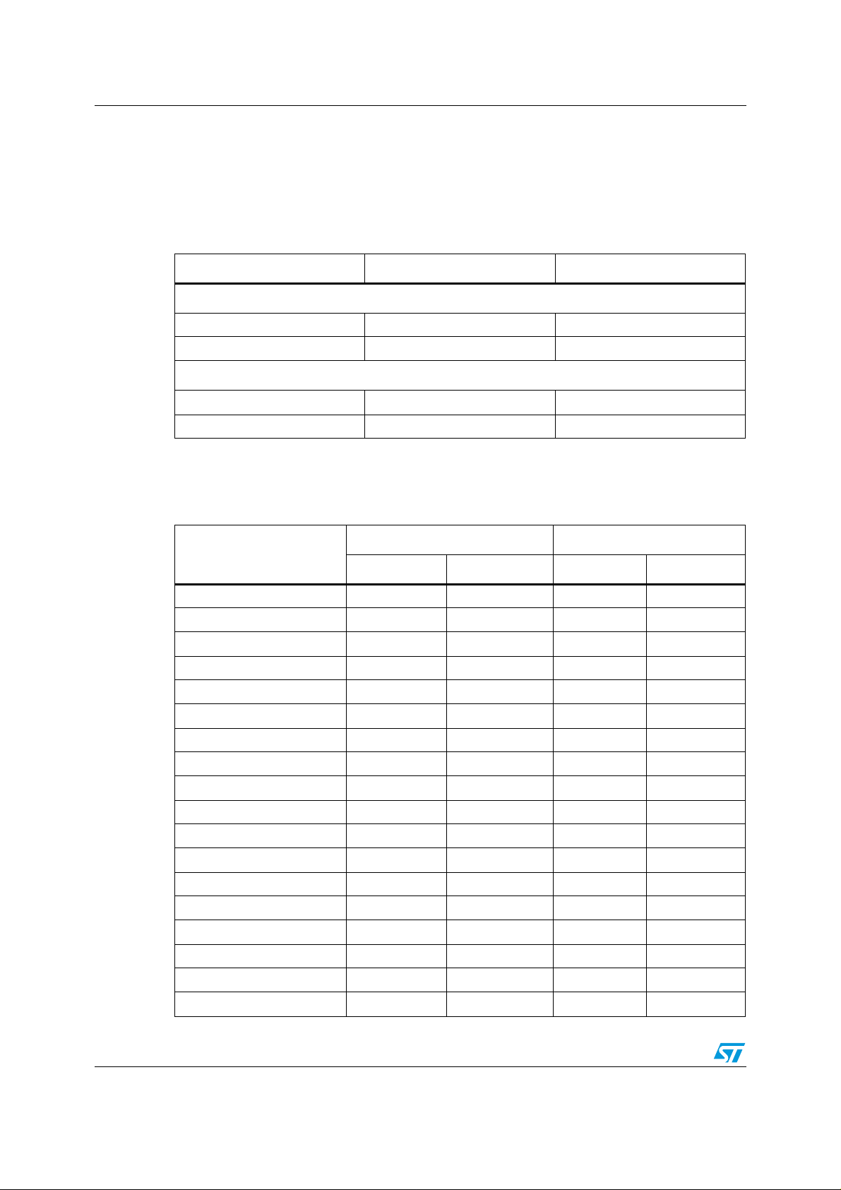
Pad dimensions (in microns)/pad positions STV7733
11 Pad dimensions (in microns)/pad positions
The reference (x=0, y=0) is the center of the die. Bump pad pitch: 68µm, minimum (on the
power output side of the die).
Table 8. Die size
Dimension Units
Die size without scribe
X 22440 µm
Y 1550 µm
Die size with scribe
X 22550 µm
Y 1660 µm
Pad placement coordinate values correspond to the center of each bump pad center.
Number of pads: 404
Table 9. Pad placement and bump dimensions (in microns)
Pad placements Bump dimensions
Lead pad name
X Y X Y
(1)
OUT320 -10845.9 600.6 51.0 73.1
OUT319 -10777.9 600.6 51.0 73.1
OUT318 -10709.9 600.6 51.0 73.1
OUT317 -10641.9 600.6 51.0 73.1
OUT316 -10573.9 600.6 51.0 73.1
OUT315 -10505.9 600.6 51.0 73.1
OUT314 -10437.9 600.6 51.0 73.1
OUT313 -10369.9 600.6 51.0 73.1
OUT312 -10301.9 600.6 51.0 73.1
OUT311 -10233.9 600.6 51.0 73.1
OUT310 -10165.9 600.6 51.0 73.1
OUT309 -10097.9 600.6 51.0 73.1
OUT308 -10029.9 600.6 51.0 73.1
OUT307 -9961.9 600.6 51.0 73.1
OUT306 -9893.9 600.6 51.0 73.1
OUT305 -9825.9 600.6 51.0 73.1
OUT304 -9757.9 600.6 51.0 73.1
OUT303 -9689.9 600.6 51.0 73.1
14/28
Page 15
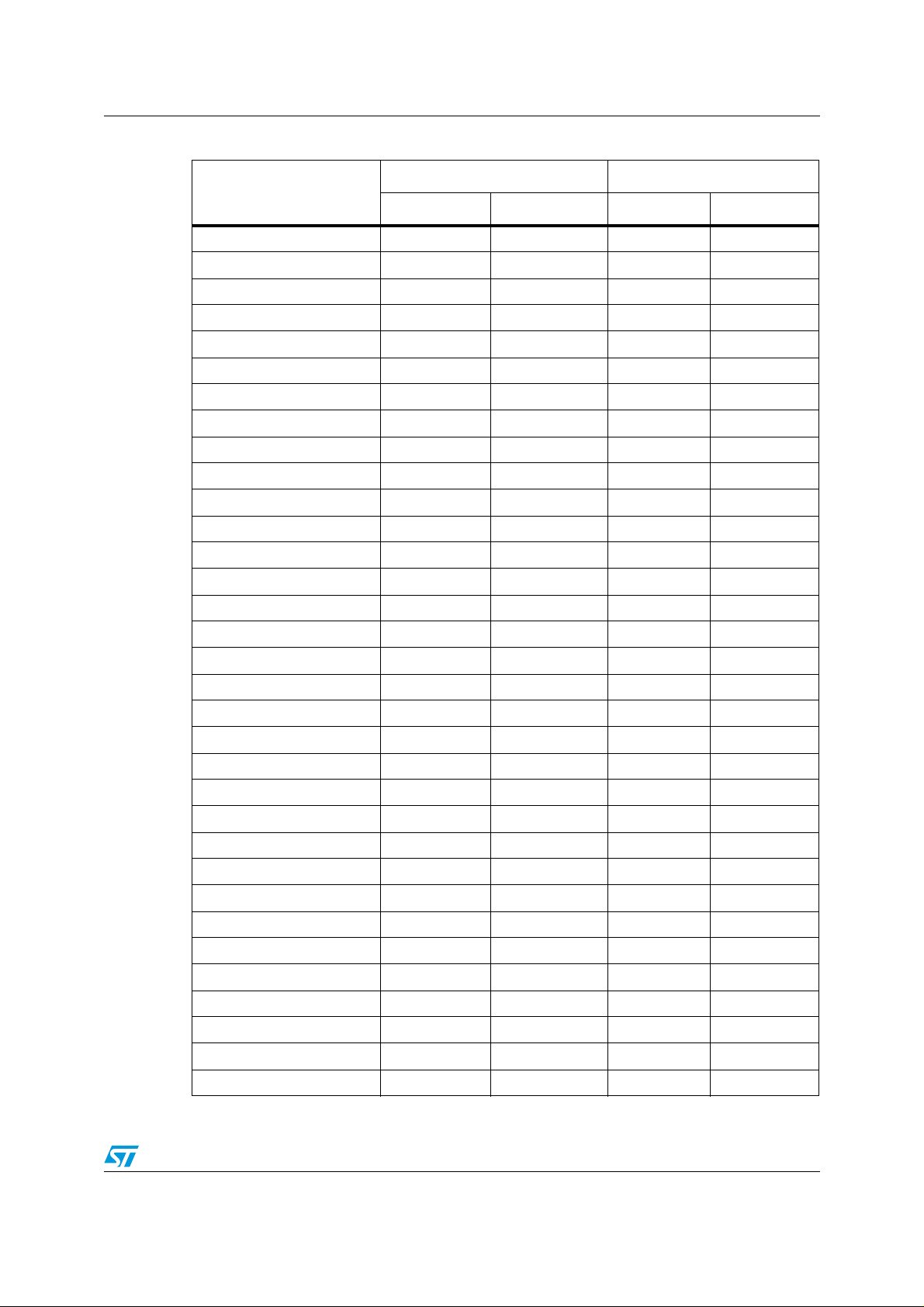
STV7733 Pad dimensions (in microns)/pad positions
Table 9. Pad placement and bump dimensions (in microns) (continued)
Pad placements Bump dimensions
Lead pad name
X Y X Y
OUT302 -9621.9 600.6 51.0 73.1
OUT301 -9553.9 600.6 51.0 73.1
OUT300 -9485.9 600.6 51.0 73.1
OUT299 -9417.9 600.6 51.0 73.1
OUT298 -9349.9 600.6 51.0 73.1
OUT297 -9281.9 600.6 51.0 73.1
OUT296 -9213.9 600.6 51.0 73.1
OUT295 -9145.9 600.6 51.0 73.1
OUT294 -9077.9 600.6 51.0 73.1
OUT293 -9009.9 600.6 51.0 73.1
OUT292 -8941.9 600.6 51.0 73.1
OUT291 -8873.9 600.6 51.0 73.1
(1)
OUT290 -8805.9 600.6 51.0 73.1
OUT289 -8737.9 600.6 51.0 73.1
OUT288 -8669.9 600.6 51.0 73.1
OUT287 -8601.9 600.6 51.0 73.1
OUT286 -8533.9 600.6 51.0 73.1
OUT285 -8465.9 600.6 51.0 73.1
OUT284 -8397.9 600.6 51.0 73.1
OUT283 -8329.9 600.6 51.0 73.1
OUT282 -8261.9 600.6 51.0 73.1
OUT281 -8193.9 600.6 51.0 73.1
OUT280 -8125.9 600.6 51.0 73.1
OUT279 -8057.9 600.6 51.0 73.1
OUT278 -7989.9 600.6 51.0 73.1
OUT277 -7921.9 600.6 51.0 73.1
OUT276 -7853.9 600.6 51.0 73.1
OUT275 -7785.9 600.6 51.0 73.1
OUT274 -7717.9 600.6 51.0 73.1
OUT273 -7649.9 600.6 51.0 73.1
OUT272 -7581.9 600.6 51.0 73.1
OUT271 -7513.9 600.6 51.0 73.1
OUT270 -7445.9 600.6 51.0 73.1
15/28
Page 16
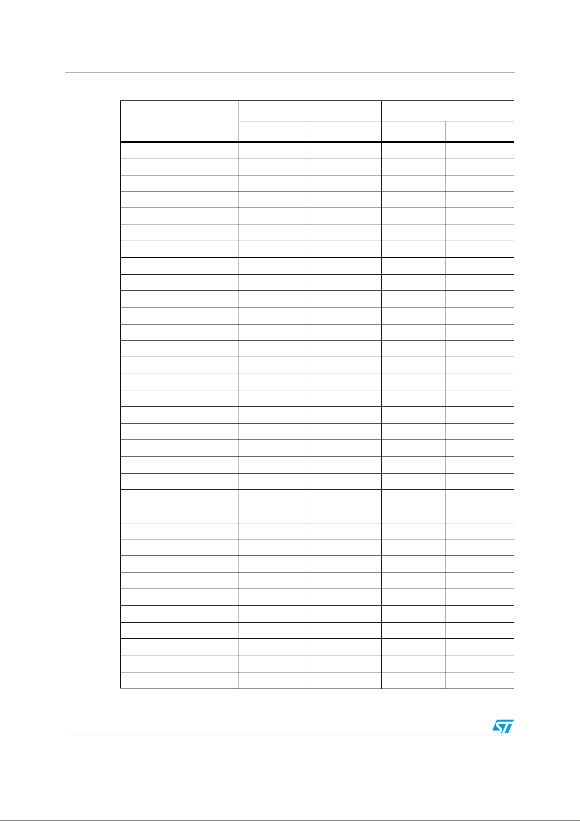
Pad dimensions (in microns)/pad positions STV7733
Table 9. Pad placement and bump dimensions (in microns) (continued)
Pad placements Bump dimensions
Lead pad name
X Y X Y
OUT269 -7377.9 600.6 51.0 73.1
OUT268 -7309.9 600.6 51.0 73.1
OUT267 -7241.9 600.6 51.0 73.1
OUT266 -7173.9 600.6 51.0 73.1
OUT265 -7105.9 600.6 51.0 73.1
OUT264 -7037.9 600.6 51.0 73.1
OUT263 -6969.9 600.6 51.0 73.1
OUT262 -6901.9 600.6 51.0 73.1
OUT261 -6833.9 600.6 51.0 73.1
OUT260 -6765.9 600.6 51.0 73.1
OUT259 -6697.9 600.6 51.0 73.1
OUT258 -6629.9 600.6 51.0 73.1
(1)
OUT257 -6561.9 600.6 51.0 73.1
OUT256 -6493.9 600.6 51.0 73.1
OUT255 -6425.9 600.6 51.0 73.1
OUT254 -6357.9 600.6 51.0 73.1
OUT253 -6289.9 600.6 51.0 73.1
OUT252 -6221.9 600.6 51.0 73.1
OUT251 -6153.9 600.6 51.0 73.1
OUT250 -6085.9 600.6 51.0 73.1
OUT249 -6017.9 600.6 51.0 73.1
OUT248 -5949.9 600.6 51.0 73.1
OUT247 -5881.9 600.6 51.0 73.1
OUT246 -5813.9 600.6 51.0 73.1
OUT245 -5745.9 600.6 51.0 73.1
OUT244 -5677.9 600.6 51.0 73.1
OUT243 -5609.9 600.6 51.0 73.1
OUT242 -5541.9 600.6 51.0 73.1
OUT241 -5473.9 600.6 51.0 73.1
OUT240 -5405.9 600.6 51.0 73.1
OUT239 -5337.9 600.6 51.0 73.1
OUT238 -5269.9 600.6 51.0 73.1
OUT237 -5201.9 600.6 51.0 73.1
16/28
Page 17
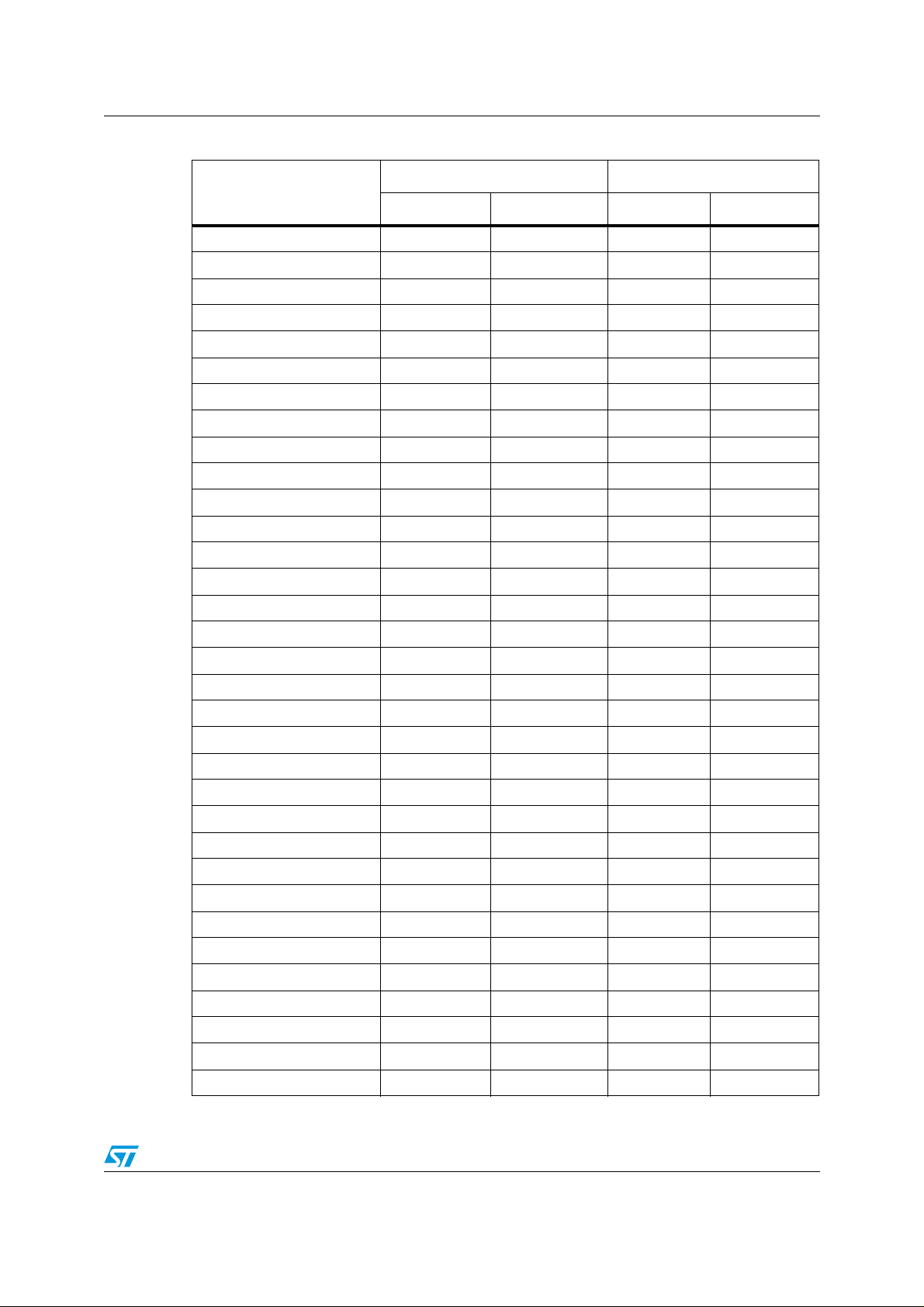
STV7733 Pad dimensions (in microns)/pad positions
Table 9. Pad placement and bump dimensions (in microns) (continued)
Pad placements Bump dimensions
Lead pad name
X Y X Y
OUT236 -5133.9 600.6 51.0 73.1
OUT235 -5065.9 600.6 51.0 73.1
OUT234 -4997.9 600.6 51.0 73.1
OUT233 -4929.9 600.6 51.0 73.1
OUT232 -4861.9 600.6 51.0 73.1
OUT231 -4793.9 600.6 51.0 73.1
OUT230 -4725.9 600.6 51.0 73.1
OUT229 -4657.9 600.6 51.0 73.1
OUT228 -4589.9 600.6 51.0 73.1
OUT227 -4521.9 600.6 51.0 73.1
OUT226 -4453.9 600.6 51.0 73.1
OUT225 -4385.9 600.6 51.0 73.1
(1)
OUT224 -4317.9 600.6 51.0 73.1
OUT223 -4249.9 600.6 51.0 73.1
OUT222 -4181.9 600.6 51.0 73.1
OUT221 -4113.9 600.6 51.0 73.1
OUT220 -4045.9 600.6 51.0 73.1
OUT219 -3977.9 600.6 51.0 73.1
OUT218 -3909.9 600.6 51.0 73.1
OUT217 -3841.9 600.6 51.0 73.1
OUT216 -3773.9 600.6 51.0 73.1
OUT215 -3705.9 600.6 51.0 73.1
OUT214 -3637.9 600.6 51.0 73.1
OUT213 -3569.9 600.6 51.0 73.1
OUT212 -3501.9 600.6 51.0 73.1
OUT211 -3433.9 600.6 51.0 73.1
OUT210 -3365.9 600.6 51.0 73.1
OUT209 -3297.9 600.6 51.0 73.1
OUT208 -3229.9 600.6 51.0 73.1
OUT207 -3161.9 600.6 51.0 73.1
OUT206 -3093.9 600.6 51.0 73.1
OUT205 -3025.9 600.6 51.0 73.1
OUT204 -2957.9 600.6 51.0 73.1
17/28
Page 18
Pad dimensions (in microns)/pad positions STV7733
Table 9. Pad placement and bump dimensions (in microns) (continued)
Pad placements Bump dimensions
Lead pad name
X Y X Y
OUT203 -2889.9 600.6 51.0 73.1
OUT202 -2821.9 600.6 51.0 73.1
OUT201 -2753.9 600.6 51.0 73.1
OUT200 -2685.9 600.6 51.0 73.1
OUT199 -2617.9 600.6 51.0 73.1
OUT198 -2549.9 600.6 51.0 73.1
OUT197 -2481.9 600.6 51.0 73.1
OUT196 -2413.9 600.6 51.0 73.1
OUT195 -2345.9 600.6 51.0 73.1
OUT194 -2277.9 600.6 51.0 73.1
OUT193 -2209.9 600.6 51.0 73.1
OUT192 -2141.9 600.6 51.0 73.1
(1)
OUT191 -2073.9 600.6 51.0 73.1
OUT190 -2005.9 600.6 51.0 73.1
OUT189 -1937.9 600.6 51.0 73.1
OUT188 -1869.9 600.6 51.0 73.1
OUT187 -1801.9 600.6 51.0 73.1
OUT186 -1733.9 600.6 51.0 73.1
OUT185 -1665.9 600.6 51.0 73.1
OUT184 -1597.9 600.6 51.0 73.1
OUT183 -1529.9 600.6 51.0 73.1
OUT182 -1461.9 600.6 51.0 73.1
OUT181 -1393.9 600.6 51.0 73.1
OUT180 -1325.9 600.6 51.0 73.1
OUT179 -1257.9 600.6 51.0 73.1
OUT178 -1189.9 600.6 51.0 73.1
OUT177 -1121.9 600.6 51.0 73.1
OUT176 -1053.9 600.6 51.0 73.1
OUT175 -985.9 600.6 51.0 73.1
OUT174 -917.9 600.6 51.0 73.1
OUT173 -849.9 600.6 51.0 73.1
OUT172 -781.9 600.6 51.0 73.1
OUT171 -713.9 600.6 51.0 73.1
18/28
Page 19
STV7733 Pad dimensions (in microns)/pad positions
Table 9. Pad placement and bump dimensions (in microns) (continued)
Pad placements Bump dimensions
Lead pad name
X Y X Y
OUT170 -645.9 600.6 51.0 73.1
OUT169 -577.9 600.6 51.0 73.1
OUT168 -509.9 600.6 51.0 73.1
OUT167 -441.9 600.6 51.0 73.1
OUT166 -373.9 600.6 51.0 73.1
OUT165 -305.9 600.6 51.0 73.1
OUT164 -237.9 600.6 51.0 73.1
OUT163 -169.9 600.6 51.0 73.1
OUT162 -101.9 600.6 51.0 73.1
OUT161 -33.9 600.6 51.0 73.1
OUT160 34.1 600.6 51.0 73.1
OUT159 102.1 600.6 51.0 73.1
(1)
OUT158 170.1 600.6 51.0 73.1
OUT157 238.1 600.6 51.0 73.1
OUT156 306.1 600.6 51.0 73.1
OUT155 374.1 600.6 51.0 73.1
OUT154 442.1 600.6 51.0 73.1
OUT153 510.1 600.6 51.0 73.1
OUT152 578.1 600.6 51.0 73.1
OUT151 646.1 600.6 51.0 73.1
OUT150 714.1 600.6 51.0 73.1
OUT149 782.1 600.6 51.0 73.1
OUT148 850.1 600.6 51.0 73.1
OUT147 918.1 600.6 51.0 73.1
OUT146 986.1 600.6 51.0 73.1
OUT145 1054.1 600.6 51.0 73.1
OUT144 1122.1 600.6 51.0 73.1
OUT143 1190.1 600.6 51.0 73.1
OUT142 1258.1 600.6 51.0 73.1
OUT141 1326.1 600.6 51.0 73.1
OUT140 1394.1 600.6 51.0 73.1
OUT139 1462.1 600.6 51.0 73.1
OUT138 1530.1 600.6 51.0 73.1
19/28
Page 20
Pad dimensions (in microns)/pad positions STV7733
Table 9. Pad placement and bump dimensions (in microns) (continued)
Pad placements Bump dimensions
Lead pad name
X Y X Y
OUT137 1598.1 600.6 51.0 73.1
OUT136 1666.1 600.6 51.0 73.1
OUT135 1734.1 600.6 51.0 73.1
OUT134 1802.1 600.6 51.0 73.1
OUT133 1870.1 600.6 51.0 73.1
OUT132 1938.1 600.6 51.0 73.1
OUT131 2006.1 600.6 51.0 73.1
OUT130 2074.1 600.6 51.0 73.1
OUT129 2142.1 600.6 51.0 73.1
OUT128 2210.1 600.6 51.0 73.1
OUT127 2278.1 600.6 51.0 73.1
OUT126 2346.1 600.6 51.0 73.1
(1)
OUT125 2414.1 600.6 51.0 73.1
OUT124 2482.1 600.6 51.0 73.1
OUT123 2550.1 600.6 51.0 73.1
OUT122 2618.1 600.6 51.0 73.1
OUT121 2686.1 600.6 51.0 73.1
OUT120 2754.1 600.6 51.0 73.1
OUT119 2822.1 600.6 51.0 73.1
OUT118 2890.1 600.6 51.0 73.1
OUT117 2958.1 600.6 51.0 73.1
OUT116 3026.1 600.6 51.0 73.1
OUT115 3094.1 600.6 51.0 73.1
OUT114 3162.1 600.6 51.0 73.1
OUT113 3230.1 600.6 51.0 73.1
OUT112 3298.1 600.6 51.0 73.1
OUT111 3366.1 600.6 51.0 73.1
OUT110 3434.1 600.6 51.0 73.1
OUT109 3502.1 600.6 51.0 73.1
OUT108 3570.1 600.6 51.0 73.1
OUT107 3638.1 600.6 51.0 73.1
OUT106 3706.1 600.6 51.0 73.1
OUT105 3774.1 600.6 51.0 73.1
20/28
Page 21
STV7733 Pad dimensions (in microns)/pad positions
Table 9. Pad placement and bump dimensions (in microns) (continued)
Pad placements Bump dimensions
Lead pad name
X Y X Y
OUT104 3842.1 600.6 51.0 73.1
OUT103 3910.1 600.6 51.0 73.1
OUT102 3978.1 600.6 51.0 73.1
OUT101 4046.1 600.6 51.0 73.1
OUT100 4114.1 600.6 51.0 73.1
OUT99 4182.1 600.6 51.0 73.1
OUT98 4250.1 600.6 51.0 73.1
OUT97 4318.1 600.6 51.0 73.1
OUT96 4386.1 600.6 51.0 73.1
OUT95 4454.1 600.6 51.0 73.1
OUT94 4522.1 600.6 51.0 73.1
OUT93 4590.1 600.6 51.0 73.1
(1)
OUT92 4658.1 600.6 51.0 73.1
OUT91 4726.1 600.6 51.0 73.1
OUT90 4794.1 600.6 51.0 73.1
OUT89 4862.1 600.6 51.0 73.1
OUT88 4930.1 600.6 51.0 73.1
OUT87 4998.1 600.6 51.0 73.1
OUT86 5066.1 600.6 51.0 73.1
OUT85 5134.1 600.6 51.0 73.1
OUT84 5202.1 600.6 51.0 73.1
OUT83 5270.1 600.6 51.0 73.1
OUT82 5338.1 600.6 51.0 73.1
OUT81 5406.1 600.6 51.0 73.1
OUT80 5474.1 600.6 51.0 73.1
OUT79 5542.1 600.6 51.0 73.1
OUT78 5610.1 600.6 51.0 73.1
OUT77 5678.1 600.6 51.0 73.1
OUT76 5746.1 600.6 51.0 73.1
OUT75 5814.1 600.6 51.0 73.1
OUT74 5882.1 600.6 51.0 73.1
OUT73 5950.1 600.6 51.0 73.1
OUT72 6018.1 600.6 51.0 73.1
21/28
Page 22
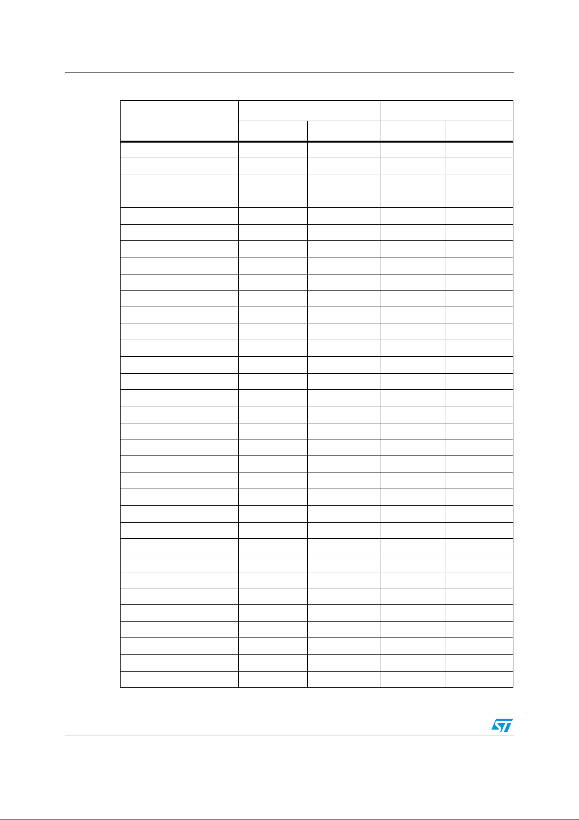
Pad dimensions (in microns)/pad positions STV7733
Table 9. Pad placement and bump dimensions (in microns) (continued)
Pad placements Bump dimensions
Lead pad name
X Y X Y
OUT71 6086.1 600.6 51.0 73.1
OUT70 6154.1 600.6 51.0 73.1
OUT69 6222.1 600.6 51.0 73.1
OUT68 6290.1 600.6 51.0 73.1
OUT67 6358.1 600.6 51.0 73.1
OUT66 6426.1 600.6 51.0 73.1
OUT65 6494.1 600.6 51.0 73.1
OUT64 6562.1 600.6 51.0 73.1
OUT63 6630.1 600.6 51.0 73.1
OUT62 6698.1 600.6 51.0 73.1
OUT61 6766.1 600.6 51.0 73.1
OUT60 6834.1 600.6 51.0 73.1
(1)
OUT59 6902.1 600.6 51.0 73.1
OUT58 6970.1 600.6 51.0 73.1
OUT57 7038.1 600.6 51.0 73.1
OUT56 7106.1 600.6 51.0 73.1
OUT55 7174.1 600.6 51.0 73.1
OUT54 7242.1 600.6 51.0 73.1
OUT53 7310.1 600.6 51.0 73.1
OUT52 7378.1 600.6 51.0 73.1
OUT51 7446.1 600.6 51.0 73.1
OUT50 7514.1 600.6 51.0 73.1
OUT49 7582.1 600.6 51.0 73.1
OUT48 7650.1 600.6 51.0 73.1
OUT47 7718.1 600.6 51.0 73.1
OUT46 7786.1 600.6 51.0 73.1
OUT45 7854.1 600.6 51.0 73.1
OUT44 7922.1 600.6 51.0 73.1
OUT43 7990.1 600.6 51.0 73.1
OUT42 8058.1 600.6 51.0 73.1
OUT41 8126.1 600.6 51.0 73.1
OUT40 8194.1 600.6 51.0 73.1
OUT39 8262.1 600.6 51.0 73.1
22/28
Page 23
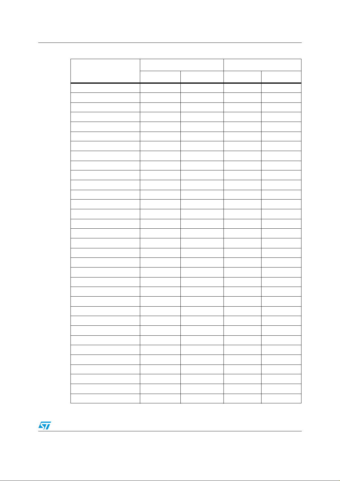
STV7733 Pad dimensions (in microns)/pad positions
Table 9. Pad placement and bump dimensions (in microns) (continued)
Pad placements Bump dimensions
Lead pad name
X Y X Y
OUT38 8330.1 600.6 51.0 73.1
OUT37 8398.1 600.6 51.0 73.1
OUT36 8466.1 600.6 51.0 73.1
OUT35 8534.1 600.6 51.0 73.1
OUT34 8602.1 600.6 51.0 73.1
OUT33 8670.1 600.6 51.0 73.1
OUT32 8738.1 600.6 51.0 73.1
OUT31 8806.1 600.6 51.0 73.1
OUT30 8874.1 600.6 51.0 73.1
OUT29 8942.1 600.6 51.0 73.1
OUT28 9010.1 600.6 51.0 73.1
OUT27 9078.1 600.6 51.0 73.1
(1)
OUT26 9146.1 600.6 51.0 73.1
OUT25 9214.1 600.6 51.0 73.1
OUT24 9282.1 600.6 51.0 73.1
OUT23 9350.1 600.6 51.0 73.1
OUT22 9418.1 600.6 51.0 73.1
OUT21 9486.1 600.6 51.0 73.1
OUT20 9554.1 600.6 51.0 73.1
OUT19 9622.1 600.6 51.0 73.1
OUT18 9690.1 600.6 51.0 73.1
OUT17 9758.1 600.6 51.0 73.1
OUT16 9826.1 600.6 51.0 73.1
OUT15 9894.1 600.6 51.0 73.1
OUT14 9962.1 600.6 51.0 73.1
OUT13 10030.1 600.6 51.0 73.1
OUT12 10098.1 600.6 51.0 73.1
OUT11 10166.1 600.6 51.0 73.1
OUT10 10234.1 600.6 51.0 73.1
OUT9 10302.1 600.6 51.0 73.1
OUT8 10370.1 600.6 51.0 73.1
OUT7 10438.1 600.6 51.0 73.1
OUT6 10506.1 600.6 51.0 73.1
23/28
Page 24
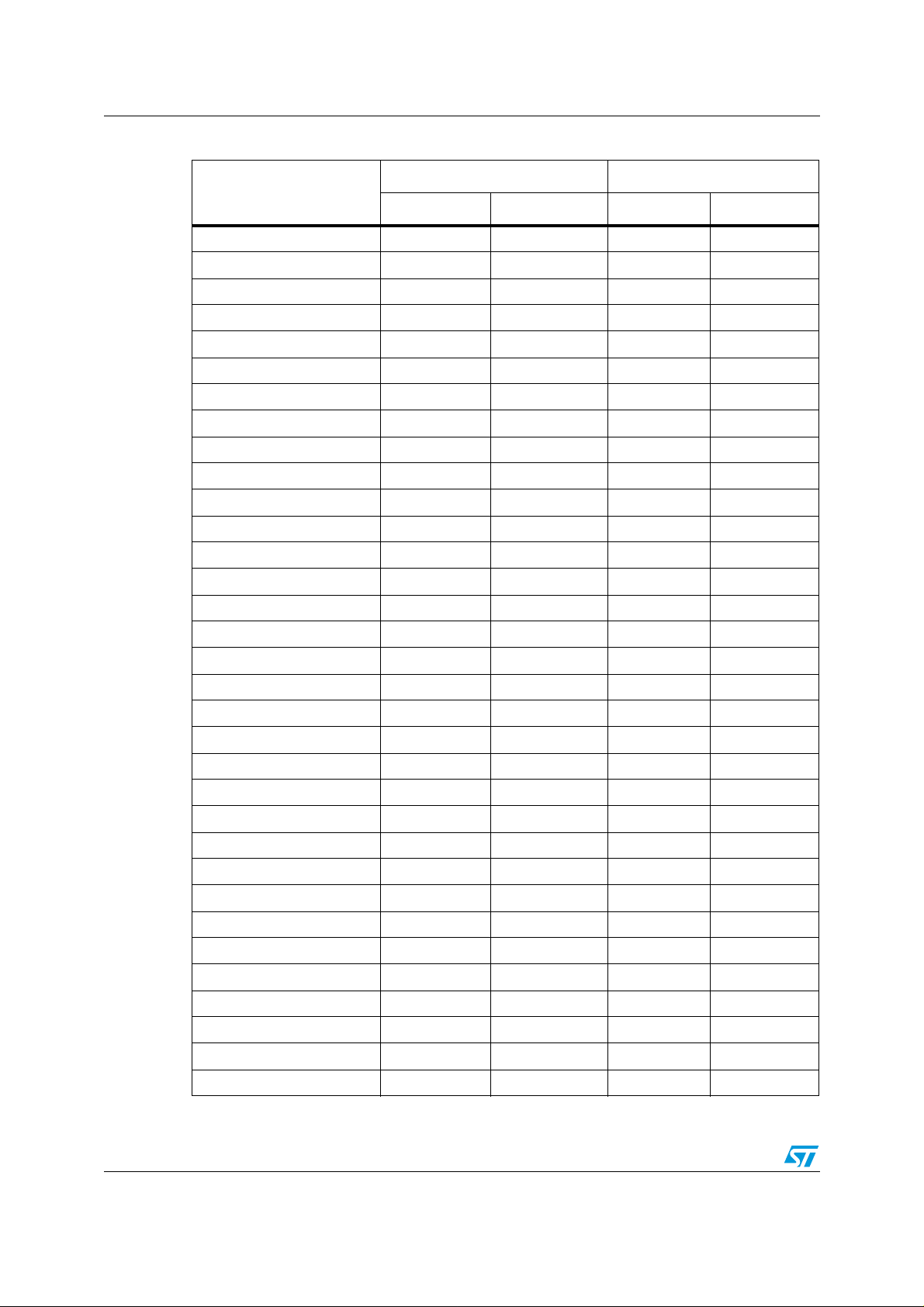
Pad dimensions (in microns)/pad positions STV7733
Table 9. Pad placement and bump dimensions (in microns) (continued)
Pad placements Bump dimensions
Lead pad name
X Y X Y
OUT5 10574.1 600.6 51.0 73.1
OUT4 10642.1 600.6 51.0 73.1
OUT3 10710.1 600.6 51.0 73.1
OUT2 10778.1 600.6 51.0 73.1
OUT1 10846.1 600.6 51.0 73.1
VSSP 11142.5 675.5 73.1 51.0
VSSP 11142.5 607.5 73.1 51.0
HVDD 11142.5 505.5 73.1 51.0
HVDD 11142.5 437.5 73.1 51.0
MVDD 11142.5 335.5 73.1 51.0
MVDD 11142.5 267.5 73.1 51.0
VSSL 11142.5 164.7 73.1 51.0
(1)
VSSS 11142.5 -107.5 73.1 51.0
VDD 11142.5 -328.9 73.1 51.0
VDD_DUMMY31 11142.5 -428.9 73.1 51.0
VDD_DUMMY30 11142.5 -496.9 73.1 51.0
VDD_DUMMY29 11142.5 -598.9 73.1 51.0
VDD_DUMMY28 11142.5 -666.9 73.1 51.0
VDD_DUMMY27 10273.7 -700.9 51.0 73.1
VDD_DUMMY26 10001.7 -700.9 51.0 73.1
VDD_DUMMY25 9729.7 -700.9 51.0 73.1
VDD_DUMMY24 9457.7 -700.9 51.0 73.1
VDD_DUMMY23 9185.7 -700.9 51.0 73.1
VDD_DUMMY22 8913.7 -700.9 51.0 73.1
VDD_DUMMY21 8641.7 -700.9 51.0 73.1
VDD_DUMMY20 8369.7 -700.9 51.0 73.1
VDD_DUMMY19 8097.7 -700.9 51.0 73.1
VDD_DUMMY18 7825.7 -700.9 51.0 73.1
VDD_DUMMY17 7276.9 -700.9 51.0 73.1
VDD 6383.4 -700.9 51.0 73.1
VSSS 6169.1 -700.9 51.0 73.1
VSSL 5897.0 -700.9 51.0 73.1
OE 5527.6 -700.9 51.0 73.1
24/28
Page 25
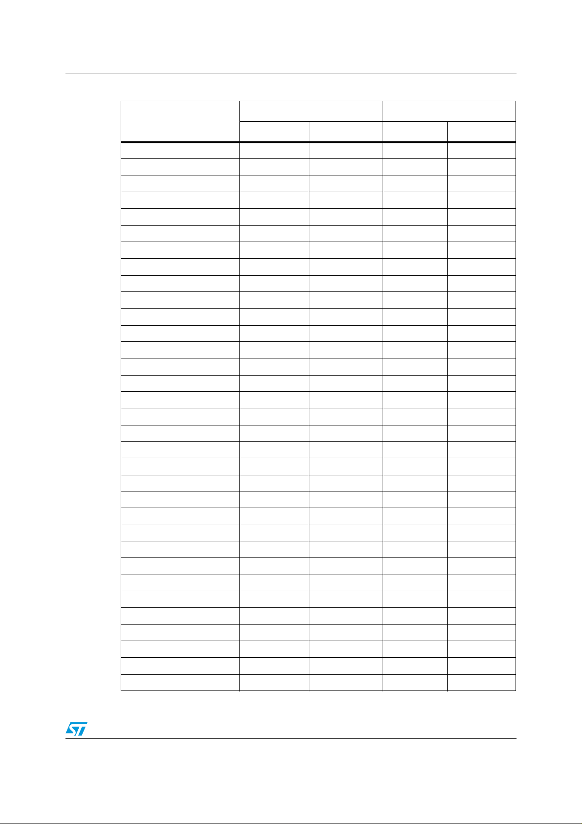
STV7733 Pad dimensions (in microns)/pad positions
Table 9. Pad placement and bump dimensions (in microns) (continued)
Pad placements Bump dimensions
Lead pad name
X Y X Y
DBD2 5157.7 -700.9 51.0 73.1
DBD1 4787.7 -700.9 51.0 73.1
DBC2 4417.8 -700.9 51.0 73.1
DBC1 4047.9 -700.9 51.0 73.1
DBC1_DUMMY2 3684.5 -700.9 51.0 73.1
DBC1_DUMMY1 2873.6 -700.9 51.0 73.1
DBB2_DUMMY2 2049.7 -700.9 51.0 73.1
DBB2_DUMMY1 1298.3 -700.9 51.0 73.1
DBB2 380.7 -700.9 51.0 73.1
DBB1 12.6 -700.9 51.0 73.1
DBA2 -355.4 -700.9 51.0 73.1
DBA1 -732.9 -700.9 51.0 73.1
(1)
VDD -801.0 -700.9 51.0 73.1
VSSS -1015.3 -700.9 51.0 73.1
VSSL -1287.4 -700.9 51.0 73.1
/CS -2180.9 -700.9 51.0 73.1
SCLK -2473.8 -700.9 51.0 73.1
/DL -2766.7 -700.9 51.0 73.1
VSSL -2834.8 -700.9 51.0 73.1
VSSS -3106.9 -700.9 51.0 73.1
VDD -3321.2 -700.9 51.0 73.1
AOC2 -3389.2 -700.9 51.0 73.1
AOC1 -3682.1 -700.9 51.0 73.1
AOC1_DUMMY1 -4378.2 -700.9 51.0 73.1
POE_DUMMY1 -5131.9 -700.9 51.0 73.1
POE -5989.1 -700.9 51.0 73.1
DIR -6282.0 -700.9 51.0 73.1
STBTEST -6574.9 -700.9 51.0 73.1
VSSL -6643.0 -700.9 51.0 73.1
VSSS -6915.1 -700.9 51.0 73.1
VDD -7129.4 -700.9 51.0 73.1
VDD_DUMMY16 -7406.3 -700.9 51.0 73.1
VDD_DUMMY15 -7678.3 -700.9 51.0 73.1
25/28
Page 26
Pad dimensions (in microns)/pad positions STV7733
Table 9. Pad placement and bump dimensions (in microns) (continued)
Pad placements Bump dimensions
Lead pad name
X Y X Y
VDD_DUMMY14 -7950.3 -700.9 51.0 73.1
VDD_DUMMY13 -8222.3 -700.9 51.0 73.1
VDD_DUMMY12 -8494.3 -700.9 51.0 73.1
VDD_DUMMY11 -8766.3 -700.9 51.0 73.1
VDD_DUMMY10 -9038.3 -700.9 51.0 73.1
VDD_DUMMY9 -9310.3 -700.9 51.0 73.1
VDD_DUMMY8 -9582.3 -700.9 51.0 73.1
VDD_DUMMY7 -9854.3 -700.9 51.0 73.1
VDD_DUMMY6 -10398.2 -700.9 51.0 73.1
VDD_DUMMY5 -10942.2 -700.9 51.0 73.1
VDD_DUMMY4 -11142.6 -666.9 73.1 51.0
VDD_DUMMY3 -11142.6 -598.9 73.1 51.0
(1)
VDD_DUMMY2 -11142.6 -496.9 73.1 51.0
VDD_DUMMY1 -11142.6 -428.9 73.1 51.0
VDD -11142.6 -328.9 73.1 51.0
VSSS -11142.6 -107.5 73.1 51.0
VSSL -11142.6 164.7 73.1 51.0
MVDD -11142.6 267.5 73.1 51.0
MVDD -11142.6 335.5 73.1 51.0
HVDD -11142.6 437.5 73.1 51.0
HVDD -11142.6 505.5 73.1 51.0
VSSP -11142.6 607.5 73.1 51.0
VSSP -11142.6 675.5 73.1 51.0
1. Tolerance: +/- 3µm
26/28
Page 27
STV7733 Ordering information
12 Ordering information
Table 10. Order codes
Part numbers Description
STV7733/BMP Tested and usawn bump wafer (u = die)
STV7733/WPB3 Gold bumped dice
13 Revision history
Table 11. Document revision history
Date Revision Changes
29-May-2007 1 Initial release
27/28
Page 28

STV7733
Please Read Carefully:
Information in this document is provided solely in connection with ST products. STMicroelectronics NV and its subsidiaries (“ST”) reserve the
right to make changes, corrections, modifications or improvements, to this document, and the products and services described herein at any
time, without notice.
All ST products are sold pursuant to ST’s terms and conditions of sale.
Purchasers are solely responsible for the choice, selection and use of the ST products and services described herein, and ST assumes no
liability whatsoever relating to the choice, selection or use of the ST products and services described herein.
No license, express or implied, by estoppel or otherwise, to any intellectual property rights is granted under this document. If any part of this
document refers to any third party products or services it shall not be deemed a license grant by ST for the use of such third party products
or services, or any intellectual property contained therein or considered as a warranty covering the use in any manner whatsoever of such
third party products or services or any intellectual property contained therein.
UNLESS OTHERWISE SET FORTH IN ST’S TERMS AND CONDITIONS OF SALE ST DISCLAIMS ANY EXPRESS OR IMPLIED
WARRANTY WITH RESPECT TO THE USE AND/OR SALE OF ST PRODUCTS INCLUDING WITHOUT LIMITATION IMPLIED
WARRANTIES OF MERCHANTABILITY, FITNESS FOR A PARTICULAR PURPOSE (AND THEIR EQUIVALENTS UNDER THE LAWS
OF ANY JURISDICTION), OR INFRINGEMENT OF ANY PATENT, COPYRIGHT OR OTHER INTELLECTUAL PROPERTY RIGHT.
UNLESS EXPRESSLY APPROVED IN WRITING BY AN AUTHORIZED ST REPRESENTATIVE, ST PRODUCTS ARE NOT
RECOMMENDED, AUTHORIZED OR WARRANTED FOR USE IN MILITARY, AIR CRAFT, SPACE, LIFE SAVING, OR LIFE SUSTAINING
APPLICATIONS, NOR IN PRODUCTS OR SYSTEMS WHERE FAILURE OR MALFUNCTION MAY RESULT IN PERSONAL INJURY,
DEATH, OR SEVERE PROPERTY OR ENVIRONMENTAL DAMAGE. ST PRODUCTS WHICH ARE NOT SPECIFIED AS "AUTOMOTIVE
GRADE" MAY ONLY BE USED IN AUTOMOTIVE APPLICATIONS AT USER’S OWN RISK.
Resale of ST products with provisions different from the statements and/or technical features set forth in this document shall immediately void
any warranty granted by ST for the ST product or service described herein and shall not create or extend in any manner whatsoever, any
liability of ST.
ST and the ST logo are trademarks or registered trademarks of ST in various countries.
Information in this document supersedes and replaces all information previously supplied.
The ST logo is a registered trademark of STMicroelectronics. All other names are the property of their respective owners.
© 2007 STMicroelectronics - All rights reserved
STMicroelectronics group of companies
Australia - Belgium - Brazil - Canada - China - Czech Republic - Finland - France - Germany - Hong Kong - India - Israel - Italy - Japan -
Malaysia - Malta - Morocco - Singapore - Spain - Sweden - Switzerland - United Kingdom - United States of America
www.st.com
28/28
 Loading...