

Page 1

®
120-MHz On-Screen Display for Monitors including
PictureBooST
Main Features
■ Horizontal frequency up to 150 kHz
■ I²C interface for microcontrollers with slave
address BA(h) in Read and Write modes
TM
and 4 True Independent Window Displays
STV9937
DATASHEET
PictureBoost
■ Pixel clock (F
ä
PIXEL1
) for the PictureBooSTä
(PB) from 30 to 60 MHz synchronised either
on Hsync or on Hfly: CLK1
■ Window position programmable by RGB or
2
I
C interface
■ Video Analog inputs with comparator on
three channels
■ Three 8 bit registers for other data,
programmable by RGB
OSD
■ On-chip Pixel Clock Generat or (F
PIXEL2
7.68 MHz to 120 MHz, CLK2
■ OSD clock synchronized on Hsync or Hfly
■ Programmable horizontal resolutions from
384 to 1524 dots per scan line
■ 4 independent windows all with character
display
■ Overlapping windows with automatic control
of display priorities and scrolling menu
effects
■ Independent and programmable displays,
positions and sizes for each window
■ Transparent or 8 programmable background
colors for each window
■ Window size up to 16 rows of 32 characters
■ Each window has its own bordering or
shadowing effects with programmable color,
height and width
) from
PDIP 24 (Plastic Dual In line Shrink Package)
ORDER CODE: STV9937P/AA
■ 496 standard and 16 multi-color characters or
graphic fonts in ROM. Character fonts can be
customized using a mask-programmable
ROM
■ Characters
● Common character height and ro w spa ce.
Character height from 18 to 127 lines and
space lines from 0 to 62 spli t abo v e and bel o w
character rows
● 12 x 18 dot matrix per character
● Display of up to 640 characters
● Programmable shadow effects for characters
in each separate window
● 32 programmable background, foreground,
blinking character colors for character s (8
possibilities per window)
● 8 selectable colors for standard characters
● Transparent and 8 selectable colors for
background
■ On-Screen Effects
● Fade-in/Fade-out effects
● Possibility of full-screen display with a
selectable color
■ Each window can be separately erased
■ Programmable common positioning to easily
control centered display
February 2004 1/49
Page 2

STV9937
Chapter 1 General Description . . . . . . . . . . . . . . . . . . . . . . . . . . . . . . . . . . . . . . . . . . . . . . . .5
1.1 Pin Descript io n ................................................................................. .. .. ..............................7
Chapter 2 Register Addressing . . . . . . . . . . . . . . . . . . . . . . . . . . . . . . . . . . . . . . . . . . . . . . .9
2.1 I²C Protocol ......................................................... .. .. ........................... .. .. ............. ... .. ............9
2.1.1 Data to Write .........................................................................................................................................................9
2.1.2 Transmission Formats ...................................... ....................................... ..............................................................9
2.1.3 Format, Window and Row Address (FWR) .........................................................................................................10
2.1.4 Format, Attribute and Column Address (FAC) ....................................................................................................10
2.1.5 Control Data, Color Codes or Character Codes .................................................................................................11
2.1.6 Configuration of Transmission Formats .............................................................................................................11
2.2 Format Chang ing ................. .......................... ... .. ............. .. .. ........................... .. .. ...............11
To change from Format A to Format B ...............................................................................................................11
To change from Format A to Format C ...............................................................................................................11
To change from Format B to Format A ...............................................................................................................11
To change from Format B to Format C ...............................................................................................................12
2.3 Read Mode ....................... ............................. .. ............................. .. ....................................12
2.4 Addressing Ma p . .. ..............................................................................................................12
Chapter 3 Window Specifications . . . . . . . . . . . . . . . . . . . . . . . . . . . . . . . . . . . . . . . . . . . .13
3.1 Enable Display ...................................................................................................................14
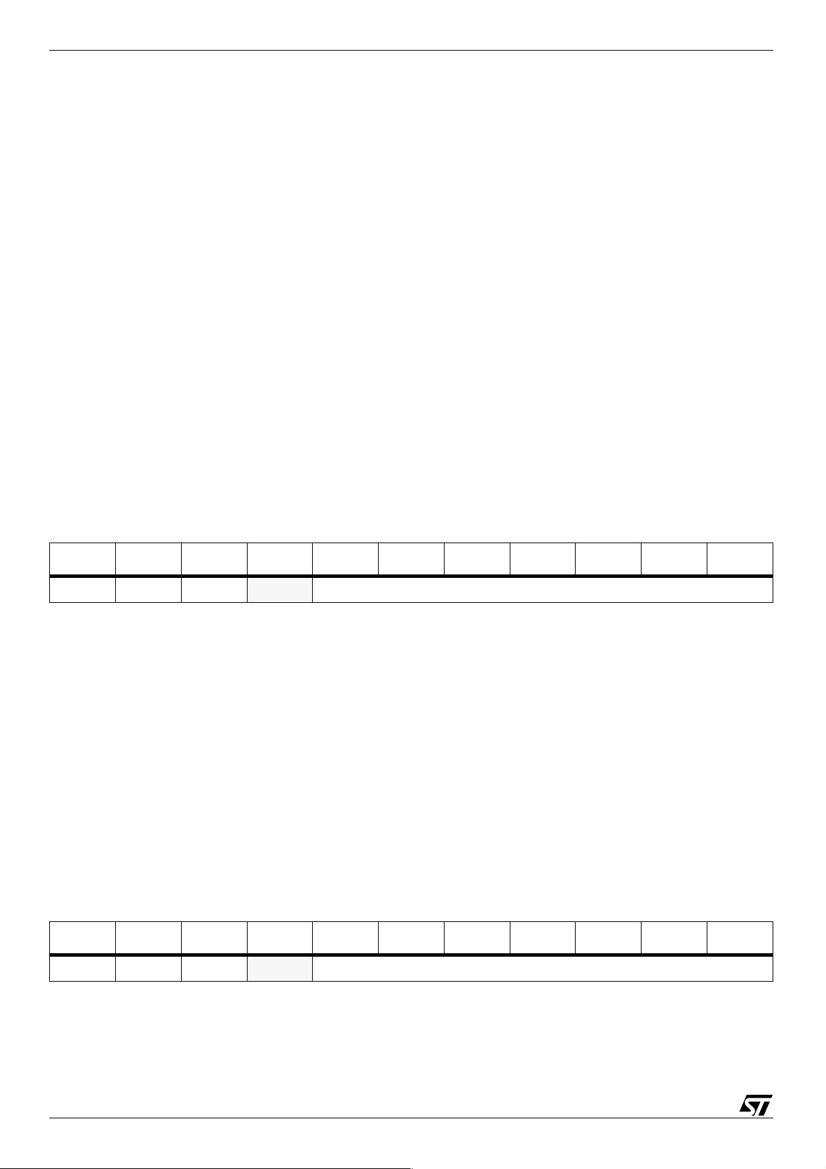
3.2 Origin Positions for the 4 Wind ows .......... .. ........................................................................14
3.2.1 General Horizontal Delay (HD) ...........................................................................................................................14
3.2.2 General Vertical Delay (VD) ................................................................................................................................14
3.3 Window Positions in the Frame ................................... .. .......................... ...........................15
3.3.1 Window Horizontal Delay ....................................................................................................................................15
3.3.2 Window Vertical Delay ........................................................................................................................................15
3.4 Window Size: Number of Characte r Rows and Character Columns ............................. .. ...16
3.4.1 Window Horizontal Size ......................................................................................................................................16
3.4.2 Window Vertical Size ..........................................................................................................................................16
3.5 Window Background Color ......... ................................................................................. .......17
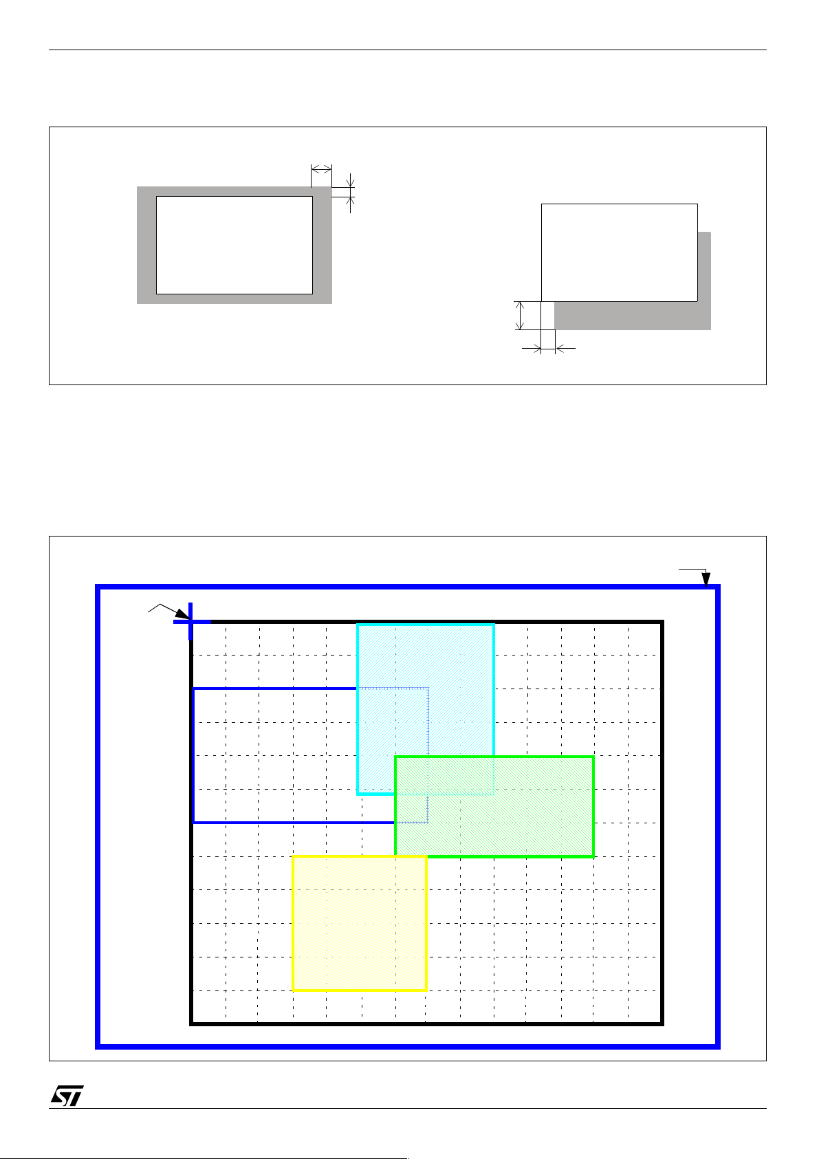
3.6 Window Bordering and Shadowing Effects ........................... ....................... .. ....................17
3.6.1 Enable Bordering or Shadowing Effects .............................................................................................................17
3.6.2 Bordering or Shadowing Selection .....................................................................................................................17
3.6.3 Border or Shadow Color .....................................................................................................................................18
3.6.4 Bordering or Shadowing Size .............................................................................................................................18
3.7 Window Display Priority Management .............................. ...................... ...................... .. ...19
Chapter 4 Character Specifications . . . . . . . . . . . . . . . . . . . . . . . . . . . . . . . . . . . . . . . . . . .20
4.1 General Description ....................................................................... ....................... .............20
4.2 Horizontal R e so l u tio n ......................... ... .. ..........................................................................20
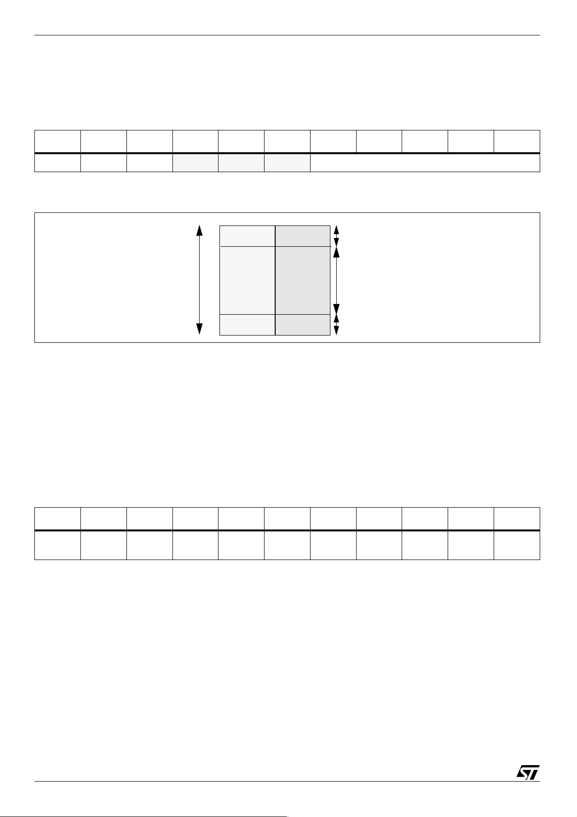
4.3 Character Height ...............................................................................................................20
2/49
Page 3

STV9937
4.4 Space Lines .......................................................................................................................21
4.5 Character Colors ................................................................................................................22
4.5.1 Character Background Color ..............................................................................................................................22
4.5.2 Character Color ...................................................................................................................................................23
4.5.3 Character Blinking Effect ....................................................................................................................................24
4.6 Character Shadowing .................................................... .. ............................................ .. .....24
4.7 Character Font ...................................................................................................................25
Chapter 5 RAM Specification . . . . . . . . . . . . . . . . . . . . . . . . . . . . . . . . . . . . . . . . . . . . . . . .26
5.1 Character Coding ...............................................................................................................26
5.2 Window Memory Allocation ............................................................. .. ............................ .. ...26
5.3 Memory Size Allocation ......................................................................................................26
5.4 Window Reset ............................................... .. ............................... ....................................28
Chapter 6 Pixel Clock Generator . . . . . . . . . . . . . . . . . . . . . . . . . . . . . . . . . . . . . . . . . . . . .29
Chapter 7 Picture BooSTTM . . . . . . . . . . . . . . . . . . . . . . . . . . . . . . . . . . . . . . . . . . . . . . . . .30
7.1 Video RGB Input Stage ......................................................................................................30
7.2 PictureBooSTTM RGB Decoder ........................................................................................31
7.2.1 Data Sent Using I²C ............................................................................................................................................31
7.2.2 Data Sent Using the RGB Channel ....................................................................................................................31
7.3 Control Reg is te r s D e s cr ip tion ................ .. ............. .. .. .............. .. .. ........................... .. .. ........33
7.4 Line and Pixel O ff s ets .......... .. ........................................ .. .. ........................... .. .. .................34
7.5 PLL Synchronised ..............................................................................................................34
Chapter 8 General OSD Programming . . . . . . . . . . . . . . . . . . . . . . . . . . . . . . . . . . . . . . . . .35
8.1 Enable OSD .......................................................................................................................35
8.2 Fade-in and Fade-out Effect ....................... ........................ ...............................................35
8.3 Full Screen Display ..................................... .................. .................. ................... ................35
8.4 Signal Polarity and Triggering ...........................................................................................36
Vertical Sync Triggering (VS input) .....................................................................................................................36
Horizontal Sync Triggering (HSYNC input) .........................................................................................................36
RGB Output Polarity (ROUT, GOUT and BOUT outputs) ...................................................................................36
Fast Blanking Output Polarity (FBLK output) ......................................................................................................37
8.5 Reset ..... ............... ................ ............. ................ ............... ................ ............. .....................37
Power On Reset .................................................................................................................................................37
Soft Reset ...........................................................................................................................................................37
PLL Register Reset .............................................................................................................................................37
Chapter 9 Registers . . . . . . . . . . . . . . . . . . . . . . . . . . . . . . . . . . . . . . . . . . . . . . . . . . . . . . . .38
3/49
Page 4

STV9937
9.1 Register Specification ........................................................................................................38
Chapter 10 Application Hints . . . . . . . . . . . . . . . . . . . . . . . . . . . . . . . . . . . . . . . . . . . . . . . . .42
10.1 Software Hints .............................................................. .. .. ..................................................42
10.1.1 Programming Recommendations .......................................................................................................................42
10.1.2 Examples of Programming ..................................................................................................................................42
Hard reset at power-up (following a power-up) ...................................................................................................42
Change of position & size of 1 window (ex. window 3) without disable of window .............................................42
Re-allocation, reset, and writing new characters in windows ..............................................................................43
10.2 Hardware Hints ..................................................................................................................43
Chapter 11 Application Diagrams . . . . . . . . . . . . . . . . . . . . . . . . . . . . . . . . . . . . . . . . . . . . .44
Chapter 12 Electrical and Timing Characteristics . . . . . . . . . . . . . . . . . . . . . . . . . . . . . . . .45
12.1 Absolute Max im u m Ratings ............ .. ..................................................... .. ... .......................45
12.2 Operating Co nd itions ............. .. ..................................................... ... .. .......................... .. ....45
12.3 Electrical and Timing Characteristics ........................................................ .........................45
12.4 I²C Bus Characteristics .................................. ... .. .......................... ... .. .......................... .. ....46
Chapter 13 Package Mechanical Data . . . . . . . . . . . . . . . . . . . . . . . . . . . . . . . . . . . . . . . . .47
Chapter 14 Revision History . . . . . . . . . . . . . . . . . . . . . . . . . . . . . . . . . . . . . . . . . . . . . . . . . .48
4/49
Page 5

STV9937 General Description
1 General Description
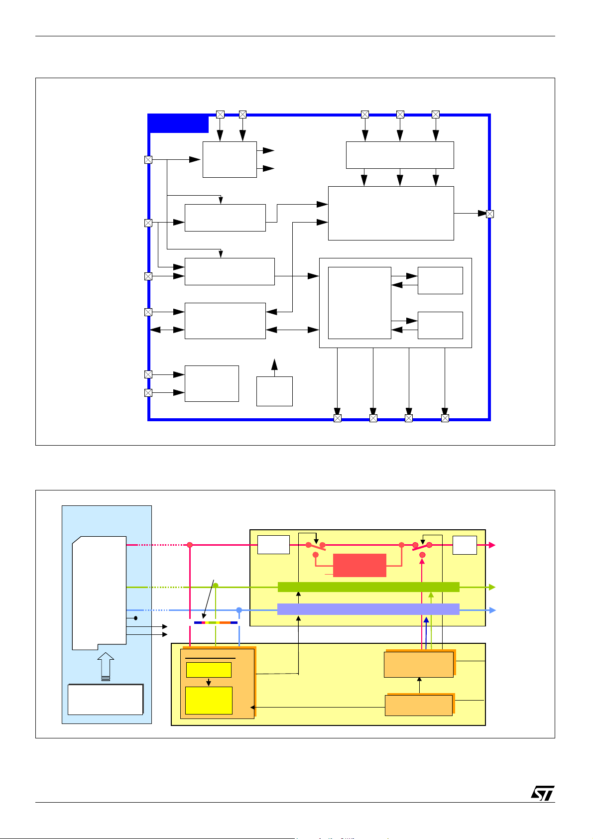
The STV9937 is an Advanced On Screen Dis pla y gener ator for CR T monit ors . It in cludes a speci fic
architecture allowing mul tiple menu displays, a built in 512 charact e r ROM and the Picture
BooST
The patented Picture BooST
screen area or even over the entir e screen.
TM
system.
TM
feature allows images to be boosted either within a window, a
Using traditional architecture (OSD + Preamp STV9212) and without any additional devices on the
TM
CRT board, Picture BooST
boosts the brightness and sharpness of the video on CRT displays
giving a TV like effect.
TM
The STV9937 can drive Picture BooST
either through the VGA cable (using RGB or DDC),
through the USB channel via the MCU or through the OSD menu (the registers can be accessed b y
the MCU via I²C).
TM
The STV9937 embeds the RGB data decoder, the Pic tur e BooST
Picture BooST
Along with the Picture BooST
TM
signal generator.
TM
and traditional OSD features, the STV9937 allows a simultaneous
Control Registers and the
display of up to four menus anywhere on the screen. Each of the four independent windows, all
displaying characters, can be overlapped and display priorities are automatically controlled.
● Window sizes and posit i ons are i ndependentl y prog r ammable as well as scrol ling men u ef fects.
● Programming of the general OSD and of the 4 windo ws is controll ed b y an I²C bus in Re ad and
Write modes, to suit the various CRT displays.
● Associated with an easily programmable character height, the internal PLL generates the
programmable pixel clock, without using a crystal oscillator, that defines the character width
making the device suitable for multi-sync applications.
● A maximum of 640 charac ters, defi ned in the mask-pr ogrammab le R OM, are distrib uted among
the 4 windows and displayed simultaneously.
Figure 1: Multi-window Concept with Character Display
5/49
Page 6
General Description STV9937
Figure 2: STV9937 Block Diagram
STV9937
HSYNC
TEST1
TEST2
VS
HFLY
SCL
SDA
STV9937
PB Sequencer
OSD Sequencer
I2C Interface
And Registers
Test
RPVCO
PLL
Reset Signals
OSD Pixel Clock
PB Pixel Clock
Reset
RIN GIN
RGB Input Buffer
Picture BooST
Decoder and Generator
4 Windows
OSD
Generator
BIN
TM
PB
RAM
ROM
ROUT
ContrastContrast
TM
System Block Diagram
I2C
PreAmplifier: STV9212
OSD: STV9937
Figure 3: PictureBooST
Computer main Unit Monitor CRT board
4
2
P
I
D
S
PictureBooST™
Video Card
DDC
H Sync
V Sync
Picture booST ™
Picture booST ™
Window ™ Software
Window ™ Software
I
D
Color code
R G B Boost OSD FBlk
4
2
P
PictureBooST ™
Decoder
Window
Coordinate
register
GOUT BOUT FBLK
Boost gain
& Sharpness
OSD
OSD
generator
generator
Line PLLLine PLL
Video Amplifier AC or DC
DriveDrive
H Fly
H Sync
6/49
Page 7

STV9937 General Description
1.1 Pin Description
Figure 4: Pin Connections
AVSS
RP
VCO
AVDD
TEST1
TEST2
HFLY
VS
HSYNC
SDA
SCL
1
2
3
4
5
6
7
8
9
10
11
12
24
23
22
21
20
19
18
17
16
15
14
13
IVSS
BIN
GIN
RIN
IVDD
DVDD
DVSS
PB
BOUT
GOUT
ROUT
FBLK
Table 1: Pin Descriptions
N° Pin Name Direction Digital/Analog Function
1 AVSS - Supply Analog Ground
2 RP I/O Analog for VCO
3 VCO I/O Analog for VCO
4 AVDD - Supply Analog Power Supply
5 TEST1 Input Digital Remains at 0 (for test purposes only)
6 TEST2 Input Digital Remains at 0 (for test purposes only)
7 HFLY Input Digital Horizontal Flyback Input
8 VS Input Digital Vertical Synchronization Input
9 HSYNC Input Digital Hor i zontal Synchronization Input
10 SDA I/O Digital Serial Data of I²C bus
11 SCL Input Digital Serial Clock of I²C bus
11 DVDD - Supply Digital Power Supply
12 N/C - - 13 FBLK Output Digit al Fast Blanking Output
14 ROUT Output Digital OSD Red Color Output
15 GOUT Output Digital OSD Green Color Output
16 BOUT Output Digital OSD Blue Color Output
17 PB Output Digital
18 DVSS - Supply Digital Ground
PictureBooST
7/49
TM
Output
Page 8

General Description STV9937
Table 1: Pin Descriptions (Continued)
N° Pin Name Direction Digital/Analog Function
19 DVDD - Supply Digital Power Supply
20 IVDD - Supply Power Supply for Video Input
21 RIN Input Analog VGA Signal Input, Red Channel
22 GIN Input Analog VGA Signal Input, Green Channel
23 BIN Input Analog VGA Signal Input, Blue Channel
24 IVSS - Supply Ground for Video Input
8/49
Page 9

STV9937 Register Addressing
2 Register Addressing
All OSD control registers are located in Wi ndow 0, Row 0. PictureBooSTTM control registers are
located in Window 0, Row 1. All color-boxes data are located in Window 0, Row 2.
Three formats are available: A, B and C, as described in the I²C protocol (see Section 2.1: I²C
Protocol).
All addresses (FAC and FWR bytes) are based on Formats A or B, and are written in hexadecimal
format.
2.1 I²C Protocol
The serial interface with t he microcontroller is an I²C bus with 2 wires: SCL and SD A. The OSD is a
slav e circuit with 2 modes: Write and Read. The sla v e address of the OSD is BAh in write mode and
BBh in read mode.
2.1.1 Data to Write
In the OSD, the I²C bus is used to write - read:
● the contro l data
● the character codes and their respective color codes
● the color-boxes (8 color-boxes per window).
A color-box contains the character color, character background color and blink data. There are 8
color-boxes for each OSD window which are used to define the colors available for all the
characters of the given OSD window. 3 bits are required to code the 8 color-boxes. These bits are
the color code.
For more information, refer to Section 4.5: Character Colors on page 22.
Each character code is related to its own window, row and column. Consequently, the protocol of
the I²C transmission inclu des this information (window, ro w and column) to define the position of t he
character on the screen. These 3 piec es of information about the position are tr ansmitted in 2 b ytes .
As each character on the screen has its own color code, the same protocol is used to write all the
color codes and character codes. Only the attribute bit called ‘A’ allows the character codes to be
distinguished from the color co des corresponding to one position on the screen.
The control data is also written with the same protocol using windows, rows and columns. Window
0 is reserved for control data and color codes.
2.1.2 Transmission Formats
There are 3 transmission formats to suit the amount of data to update. The transmission format is
coded in the “window/row/column” bytes.
Format A is suitab le for updating small amounts of data whi ch are allocated to different windo w, row
and column addresses.
Format B is recommended for updating data for the same window and the same row address, but
with a different column address and when changing the Character/Color-box attribute (bit A), or
when writing to a different I²C control register.
Format C is appropriate for updating large amounts of data from a full window or full screen. The
window, row and column addresses are incremented automatically when this format is applied.
Data is written to fill all the allocation memory of the windows .
9/49
Page 10

Register Addressing STV9937
The transmission formats are as follows:
1. Format A: S-FWR-FAC-D
® FWR-FAC-D ® FWR-FAC-D ® FWR-FAC-D...Stop
2. Format B: S-FWR-FAC-D
3. Format C: S-FWR-FAC-D
® FAC-D ® FAC-D ® FAC-D...Stop
® D ® D ®D...Stop
Where:
S = Slave address = BAh
FWR = Format, Window and Row address
FAC = Format, Attribute and Column address
D = CTRL Control data (8 bits), CB Color codes (3 bits) or RC Character codes (9 bits).
In Format C, t he order of automati c incrementat ion for data D i s first t he column v alue , then t he ro w
value, and then the window value.
Table 2: Various Bytes coded in the I²C Transmission
Byte Bit 7 Bit 6 Bit 5 Bit 4 Bit 3 Bit 2 Bit 1 Bit 0
FWR
FAC
D: Control Data (in window 0 only) CTRL[7:0]
D: Color Code and Character Code MSB 0 0 0 RC[8] 0 CB[2:0]
D: Character Code LSBs RC[7:0]
1
0
W[2:0] R[3:0]
F A C[4:0]
2.1.3 Format, Window and Row Address (FWR)
Bit 7 indicates the ‘Window & Row’ byte when set to 1.
W[2:0]: Window Number
000: Control Data and Color Codes
001: Window 1
010: Window 2
011: Window 3
100: Window 4
R[3:0]: Row Numbers from 0 to 15. Each window has a maximum number of 16 rows.
2.1.4 Format, Attribute and Column Address (FAC)
Bit 7 indicates the ‘Attrib ute & Column’ byte when set to 0.
F: Format
0: Format A or B
1: Format C
A: Transmission of character code or color code
0: Character Code
1: Color Code and Character Code MSB
When reading or writing control data and/or character codes, bit A must be set to 0. For color code
and character code MSB, bit A must be set to 1.
10/49
Page 11

STV9937 Register Addressing
C[4:0]: Column Number
There are 32 possible columns .
00000: 1 column
11111: 32 columns
2.1.5 Control Data, Color Codes or Character Codes
Color codes are stored on 3 bits. Control data is stored on 8 bits and Charact er codes are stored on
9 bits.
2.1.6 Configuration of Transmission Formats
Table 3: Configuration of Transmission Formats
Byte Format Bit 7 Bit 6 Bit 5 Bit 4 Bit 3 Bit 2 Bit 1 Bit 0
Address bytes
for Characters
Codes
Address bytes
for Color Codes
Windows & Rows
Column (A and B)
Column (C)
Windows & Rows
Column (A and B)
Column (C)
All formats must start with the S, FWR and FAC bytes.
2.2 Format Changing
To change from Format A to Format B
S-FWR[0]- FAC[0] -D[0] ® FWR[1]- FAC[1]- D[1] ® FWR[2]- FAC[2]- D[2] ® FAC[3]- D[3] ® FAC[4]D[4]
® FAC[5]- D[5]...
The F bit from the FAC byte is alwa ys 0 in this case.
FWR
FAC
FAC
FWR
FAC
FAC
A, B or C 1 W[2:0] R[3:0]
A or B 0 0 0 C[4:0]
C 0 1 0 C[4:0]
A, B or C 1 W[2:0] R[3:0]
A or B 0 0 1 C[4:0]
C 0 1 1 C[4:0]
To change from Format A to Format C
S - FWR[0]- FAC[0]- D[0] ® FWR[1]- FAC[1]- D[1] ® FWR[2]- FAC[2]- D[2] ® D[3] ® D[4] ® D[5]...
The “F” bit from the FAC byte is as follo w s:
F[0] = F[1] = “0”
F[2] = “1”
To change from Format B to Format A
S - FWR[0]- FAC[0]-D[0]® FAC[1]- D[1] ® FAC[2]-D[2] ® FWR[3]- FAC[3]- D[3] ® FWR[4]- FAC[4]D[4]...
The F bit from the FAC byte is alwa ys 0 in this case.
11/49
Page 12

Register Addressing STV9937
To change from Format B to Format C
S - FWR[0]- FAC[0]- D[0] ® FAC[1]- D[1] ® FAC[2]- D[2] ® D[3] ® D[4]...
The “F” bit from the FAC byte is as follows: F[0] = F[1] = “0” and F[2] = “1”
It is not possible to change from Format C back to Format A or B.
Figure 5: Format Changing Sequences
Start
start
2.3 Read Mode
The transmission format is shown as below:
Start - S(w) - FWR- FAC - Stop - Start - S(r) - D
Where:
S(w) = Slave address in write mode = BAh = 10111010,
S(r) = Slave address in read mode = BBh = 10111011.
Registers and data in RAM are readable.
This mode is useful when developing OSD applications.
2.4 Addressing Map
Format A
Format C
Format B
® D ® D ® D...Stop
Table 4: Window Addressing Map
Window Row Column Data
Window 0 Row 0 Columns 0 to 31 Control Data (8 bits)
Window 0 Row 1 Columns 0 to 31
Window 0 Row 2 Columns 0 to 31 Color-boxes (8 bits)
Windows 1, 2, 3 and 4 Rows 0 to n (n = 15 max.) Columns 0 to m (m = 31 max.) Characters Coding (12 bits)
12/49
PictureBooST
TM
Data
Page 13

STV9937 Window Specifications
3 Window Specifications
Four different independent windows with separate character displays can be simultaneously
display ed on screen . It is pos sib le to ha v e o v erlapping windo ws with an automat ic control of display
priorities: downscale priorities from Window 4 to Window 1.
Window 1 is well-ad apted for the OSD general menu.
The 4 windows, each with its own character display, can be positioned anywhere on the screen.
The following characteristics are defined for each window:
● Enable Display
● Position
● Size, adjustable with memory allocation
● Background Color
● Bordering or Shadowing effects with programmable color, height and width.
Figure 6: Example of Window Displays
Axis
Origin
Screen
HD
Window 2
VD
Window 1
Window 3
Window 4
13/49
Page 14

Window Specifications STV9937
3.1 Enable Display
The Enable Display command for each window is selected by bits ENW1, ENW2, ENW3 and
ENW4. If the ENWi bit is set to 1, the corresponding window is displayed.
Table 5: Enable Display
FWR FAC Default Bit 7 Bit 6 Bit 5 Bit 4 Bit 3 Bit 2 Bit 1 Bit 0
80h 07h 0h ENW4 ENW3 ENW2 ENW1
3.2 Origin Positions for the 4 Windows
The 4 windows are arranged in a fr ame whose origin coordinates are t he horizontal dela y ( HD) and
the vertical delay (VD) loc ated at the upper left-hand corner of the monitor screen. When the HD
and VD values are changed, the 4 windows within the frame position are automatically shifted by
the same value. The origin (HD, VD) can be programmed anywhere on the screen. Adjusting the
origin position is used to globally reposition the OSD windows.
The advantages of this system are easi er programming, the possibility to adapt the position of all
windows at a single time without changing the relative position of each window and the possibility
for the user to program all 4 window positions.
3.2.1 General Horizontal Delay (HD)
Table 6: Origin of Windows on Horizontal Axis: Horizontal Delay
FWR FAC Default Bit 7 Bit 6 Bit 5 Bit 4 Bit 3 Bit 2 Bit 1 Bit 0
80h 04h 0h HD[6:0]
The general horizontal delay defines the horizontal position of the origin coordinate f or all four OSD
windows. The horizontal delay is selected by bits HD[6:0].
General Horizontal Offset = 50 pixels
General Horizontal Delay = HD[6:0] x 6 pixels + General Offset (i n pixels)
The default value of the horiz ontal delay is 0h (left-hand side of the moni tor screen).
3.2.2 Gen eral Vertical Delay (VD)
Table 7: Origin of Windows on Vertical Axis: Vertical Delay
FWR FAC Default Bit 7 Bit 6 Bit 5 Bit 4 Bit 3 Bit 2 Bit 1 Bit 0
80h 05h 0h VD[7:0]
The general vertical delay defines the vertical position of the origin coordinate for all four OSD
windows. The v ertical delay is selected by bits VD[7:0] . A general vertical offset of 2 scan lines is
also applied.
The range of the vertical delay is from 2 to 1022 scan lines, in steps of 4 scan lines each.
General Ver tical Delay = VD[7:0] x 4 + 2 (in scan lines)
The default value of the vertical delay is 0h (top of screen).
14/49
Page 15

STV9937 Window Specifications
3.3 Window Positions in the Frame
All values are referenced to the origin coordinates (HD, VD). For more information, refer to
Figure 6 on page 13.
3.3.1 Window Horizontal Delay
The window horizontal delay defines the horizontal start position for each separate OSD window.
This value is selected by bits HDW1[6:0] , HDW2[6:0], HDW3[6:0] and HDW4[6:0], respectively.
Table 8: Window Horizontal Delay
FWR FAC Default Bit 7 Bit 6 Bit 5 Bit 4 Bit 3 Bit 2 Bit 1 Bit 0
80h
0Ch, 11h,
16h, 1Bh
0h, 20h,
0h, 10h
HDWi[6:0]
The range of the window horizontal delay is from 0 to 1524 pixels, in steps of 12 pixels each.
Window Horizontal Delay = HDWi[6:0] x 12 pixels
The total horizontal delay of a window is:
General Horizontal Delay + HDWi[6:0] x 12 pixels; or,
HD[6:0] x 6 pixels + HDWi[6:0] x 12 pixels + (50 pixels).
The default values for the window horizontal delay for each of the four OSD windows is given in
Table 8.
3.3.2 Window Vertical Delay
The window vertical delay defines the vertical start position for each separate OSD window. This
value is selected by bits VDW1[5:0], VDW2[ 5:0], VDW3[5: 0] and VDW4[5:0], respectively.
Table 9: Window Vertical Delay
FWR FAC Default Bit 7 Bit 6 Bit 5 Bit 4 Bit 3 Bit 2 Bit 1 Bit 0
80h
0Dh, 12h,
17h, 1Ch
0h, 0h,
Ch, Ch
VDWi[5:0]
The range of the window v ertical delay i s from 0 to 63 rows of c haracters, in steps of 1 charact er row
each. It is important to note that the height of each character row is defined by the row height
parameter. For more information, refer to Section 4.4: Space Lines on page 21.
Window Vertical Delay = VDWi[5: 0] x Row_Height
The total vertical delay of a windo w is:
General Ver tical Delay + VDWi[5:0] x Row_Height (in scan lines); or,
(VD[7:0] x 4 + 2) + VDWi[5:0] x Row_Height (in scan lines).
The default values for the window vertical delay for each of the four OSD windows is given in
Table 9.
15/49
Page 16
Window Specifications STV9937
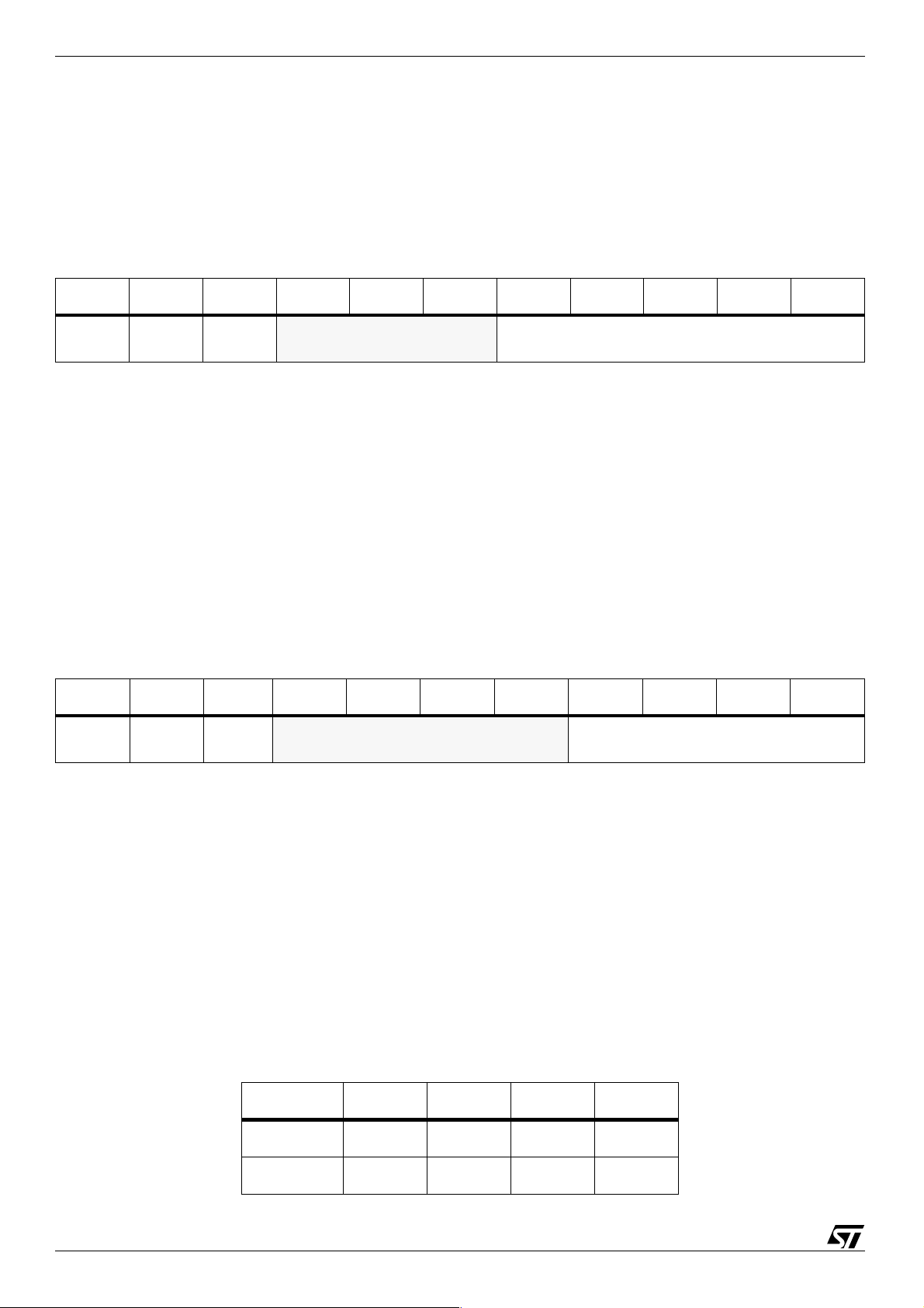
3.4 Window Size: Number of Character Rows and Character Columns
3.4.1 Window Horizontal Size
The window horizontal size defines the number of characters displayed for character row for each
separate OSD window. This value is selected by bits HSW1[4:0], HSW2[4:0], HSW3[4:0] and
HSW4[4:0], respectively.
Table 10: Window Horizontal Size
FWR FAC Default Bit 7 Bit 6 Bit 5 Bit 4 Bit 3 Bit 2 Bit 1 Bit 0
80h
0Eh, 13h,
18h, 1Dh
19h, 9h,
Fh, Fh
HSWi[4:0]
The range of the window horizontal size is from 1 to 32 characters, in steps of 1 character each.
Each character is 12 pixels long. There is an offset of 1 character.
Window Horizontal Size = HSWi[4:0] +1 characters
The default values for the window horizontal size for each of the four OSD windows is given in
Table 10.
3.4.2 Window Vertical Size
The window vertical size defines the number of character rows d isplayed for each separate OSD
window. This value is selected by bits VSW1[3:0], VSW2[3:0], VSW3[3:0] and VSW4[3:0],
respectively.
Table 11: Window Vertical Size
FWR FAC Default Bit 7 Bit 6 Bit 5 Bit 4 Bit 3 Bit 2 Bit 1 Bit 0
80h
0Fh, 14h,
19h, 1Eh
Bh, 4h,
7h, 7h
VSWi[3:0]
The range of the window v e rtical size is from 1 to 16 char acter rows, in steps of 1 charac ter row
each. It is important to note that the height of each character row is defined by the row height
parameter . F or more information, refer t o Section 4.4: Space Lines on page 21. There is an offset of
1 character row.
Window Vert ical Size = (VSWi[3:0] + 1) x Row_Height (in scan lines)
Row_Height = Character_Height + 2 x Space_Lines
The default values for the window vertical size for each of th e four OSD windows is given in
Table 11.
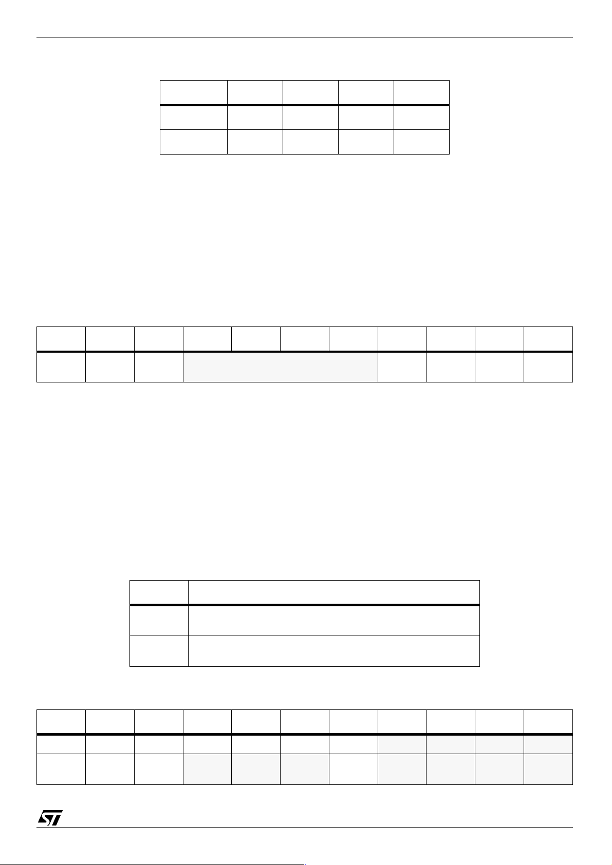
Table 12 shows an example of the origin and size of windows based on the example shown in
Figure 8,
Table 12: Example of Origin and Size of Windows
Window i HD VD HSWi VSWi
Window 1
Window 2
16/49
0274
5045
Page 17
STV9937 Window Specifications
Table 12: Example of Origin and Size of Windows
Window i HD VD HSWi VSWi
Window 3
Window 4
6463
3744
3.5 Window Background Color
The window background color for each separate OSD window is coded over 4 bits as shown in
Table 13. The first bit (Ti) specifies whether the background is tr ansparent or if a color is displayed.
If the background is tr ansparent (Ti = 1), the active video is display ed as background.
If a color is displayed (Ti = 0), the background color for each separate OSD window is coded over
the last three bits (RWi, GWi and BWi, respectively). Windows are displayed with a white
background by default (7h).
Table 13: Background Color of Each Window
FWR FAC Default Bit 7 Bit 6 Bit 5 Bit 4 Bit 3 Bit 2 Bit 1 Bit 0
80h
10h, 15h
1Ah, 1Fh
7h, 7h,
7h, 7h
Ti RWi GWi BWi
3.6 Window Bordering and Shadowing Effects
3.6.1 Enable Bordering or Shadowing Effects
Bordering or shadowing effects are enabl ed for each separate OSD window by bits ENBS1,
ENBS2, ENBS3 and ENBS4, respectively.
3.6.2 Bordering or Shadowing Selection
Either the bordering or the shadowing effect is selected for each separate OSD window by bits
BSW1, BSW2, BSW3 and BSW4, respectively.
Table 14: Bordering and Shadowing Parameter Selection
Bit Description
ENBSi
BSWi
0: No Bordering, No Shadowing (Default Value)
1: Bordering or Shadowing is select ed.
0: Bordering is selected (Default Value)
1: Shadowing is selected.
Table 15: Enable Bordering or Shadowing Effects
FWR FAC Default Bit 7 Bit 6 Bit 5 Bit 4 Bit 3 Bit 2 Bit 1 Bit 0
80h 07h 0h ENBS4 ENBS3 ENBS2 ENBS1
80h
10h, 15h
1Ah, 1Fh
0h, 0h,
0h, 0h
BSWi
17/49
Page 18
Window Specifications STV9937
3.6.3 Border or Shadow Color
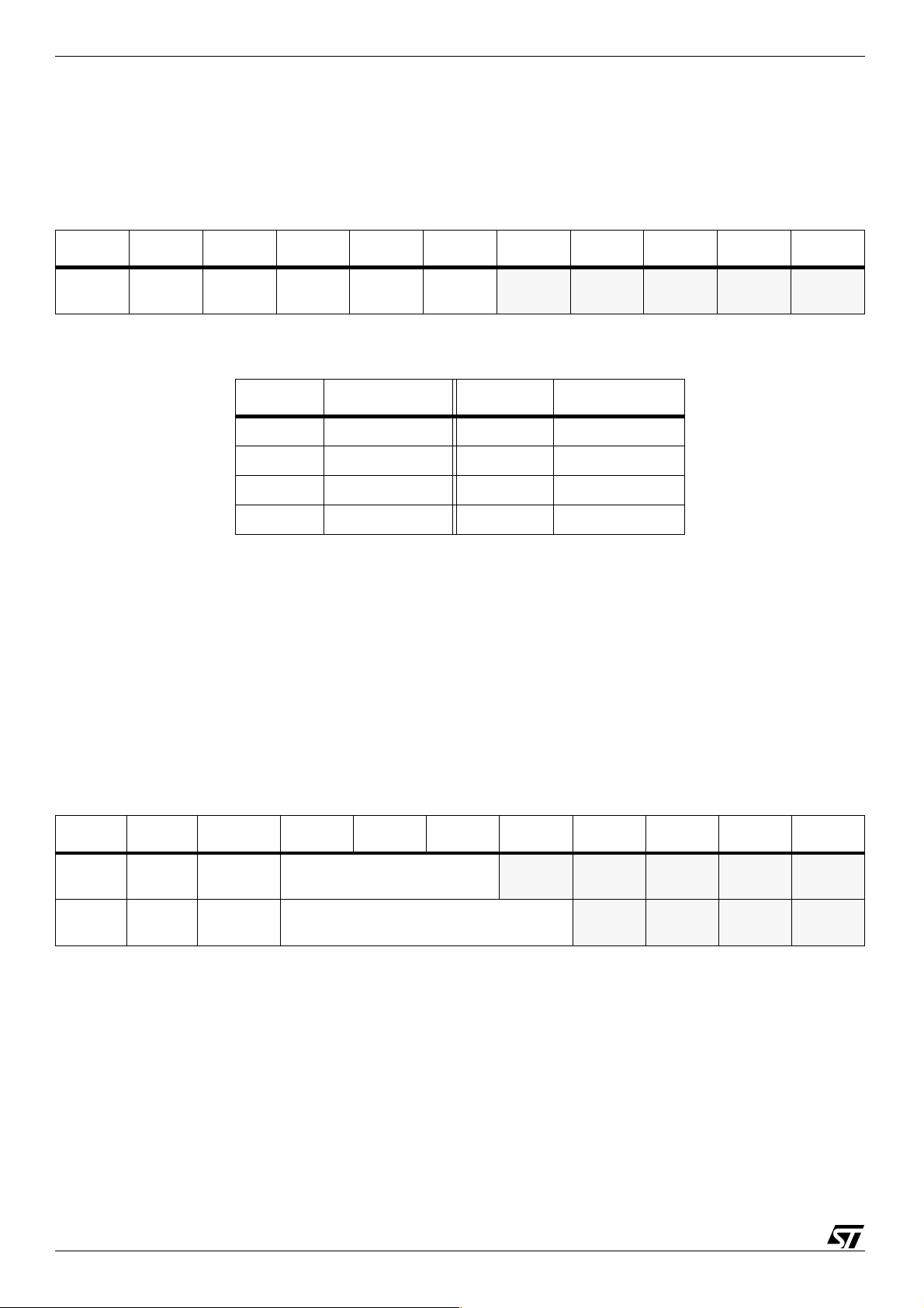
The border or shadow c olor is s eparately progr ammable f or each separa te OSD window. This value
is selected by bits WSRi, WSGi and WSBi for each of the four OSD windows. The value for each
color is shown in Table 17.
Table 16: Border or Shadow Color
FWR FAC Default Bit 7 Bit 6 Bit 5 Bit 4 Bit 3 Bit 2 Bit 1 Bit 0
80h
10h, 15h
1Ah, 1Fh
0h, 0h,
0h, 0h
WSRI WSGI WSBI
Table 17: Bordering and Shadowing Color Selection (WSRGBi)
Value Color Value Color
000 Black (Default) 100 Red
001 Blue 101 Magenta
010 Green 110 Yellow
011 Cyan 111 White
3.6.4 Bordering or Shadowing Size
The size of the bordering or shadowing width is separately programmable for each separate OSD
window. This value is selected by bits BSWWi[2:0] for each of the four OSD windows. The width
size is from 0 to 14 pixels, in steps of 2 pixels each.
Width Size = BSWWi[2:0] x 2 pixels
The size of the bordering or shadowing he ight is selected by bits BSHWi[3:0] for each of the four
windows. The height size is from 0 to 30 lines, in steps of 2 scan lines each.
Height Size = BSHWi[3:0] x 2 scan lines.
Table 18: Bordering or Shadowing Size
FWR FAC Default Bit 7 Bit 6 Bit 5 Bit 4 Bit 3 Bit 2 Bit 1 Bit 0
80h
80h
0Eh, 13h
18h, 1Dh
0Fh, 14h
19h, 1Eh
0h, 0h,
0h, 0h
0h, 0h,
0h, 0h
BSWWi[2:0]
BSHWi[3:0]
18/49
Page 19
STV9937 Window Specifications
Figure 7: Illustration of Window Bordering and Shadowing Effects
M pixels
Window Shadowing
N scan lines
N scan lines
Window Bordering
M pixels
3.7 Window Display Priority Management
The OSD windows are displayed with the following priority: Window 4 (top), 3, 2 and 1 (bottom).
This order of priority is shown the e xample given in Figure 8.
Figure 8: Example of Window Displays
Screen
Axis
Origin
VD
HD
Window 2
Window 1
Window 3
Window 4
19/49
Page 20
Character Sp ecifications STV9937
4 Character Specifications
4.1 General Description
There are:
● 496 monochrome characters and 16 multi-color characters in ROM
● 32 to 127 characters per line
● character height varies between 18 and 127 scan lines
● 0 to 62 scan space lines between character rows, with the same number of lines above and
below the rows of characters.
With the possibility to select:
● blinking effect for each character
● shadowing effect for characters in each window
● background and foreg round character colors: for each character, among a Color-shop of 8
Color-boxes per window. There is a Color-shop for each window. The Color-boxes define the
background colors and the foreground character colors and blinking effect.
4.2 Horizontal Resolution
T able 19: Horizontal Resolution
FWR FAC Default Bit 7 Bit 6 Bit 5 Bit 4 Bit 3 Bit 2 Bit 1 Bit 0
80h 01h 20h HR[6:0]
The horizontal resolution defines the number of pixels per line expressed in characters unit. This
value is selected by bits HR[6:0].
The range of the horizontal resolution is from 32 to 127 characters, i n steps of one character each.
The default value is 32 characters per line (20h). If bits HR[6:0] are prog rammed with a value less
than 32, the horizontal resoluti on wil l be 32 characters per line (minimum value).
HR[6:0] = Number of characters per line
It is important that the maximum pixel frequency must be respected (CLK2= 120 MHz maximum).
As each character is 12 pixels long, the number of pixels per line v aries from 384 to 1524. F or more
information, refer to Section 6: Pixel Clock Generator on page 29.
4.3 Character Height
Table 20: Vertical Character Height
FWR FAC Default Bit 7 Bit 6 Bit 5 Bit 4 Bit 3 Bit 2 Bit 1 Bit 0
80h 02h 12h CH[6:0]
The vertical height defines the number of scan lines used to di splay the characters. This value is
selected by bits CH[6:0].
20/49
Page 21
STV9937 Character Specifications
The range of the vertical height is from 18 to 127 lines.
CH[6:0] = Number of scan lines used to display the characters
The characters stored in ROM are coded on 18 lines. If bits CH[6:0] are programmed with a value
less than 18, the characters will be automatic ally displ a y ed with a height of 18 scan li nes (minim um
value).
When a multiple of 18 scan lines are dis pla y ed, all R OM lines are repeated N number of ti mes, with
N in the range of 1 to 7, so as not to exceed the displa y of 127 scan lines. For example, if CH[6:0] =
36, each ROM line is repeated twice.
If the number of scan lines displayed is not a multiple of 18, certain ROM lines are repeated more
often than others, as shown in Table 21. For example, if CH[6:0] = 40, each ROM line is repeated
twice and ROM lines 3, 7, 10 and 14 are repeated three times.
Table 21 shows which ROM lines, from 0 to 17, are repeated depending on the CH[6:0] value.
T a ble 21: Repeated ROM Lines
CH Value A01234567891011121314151617
18, 36, 54, 72, 90, 108, 126 0
19, 37, 55, 73, 91, 109, 127 1 R
20, 38, 56, 74, 92 ,110, 2 R R
21, 39, 57, 75, 93, 111 3 R R R
22, 40, 58, 76, 94, 112 4 R R R R
23, 41, 59, 77, 95, 113 5 R R R R R
24, 42, 60, 78, 96, 1146RRRRRR
25, 43, 61, 79, 97, 115 7 R R R R R R R
26, 44, 62, 80, 98, 116 8 R R R R R R R R
27, 45, 63, 81, 99, 117 9 R R R R R R R R R
28, 46 ,64, 82, 100, 118 10 R R R R R R R R R R
29, 47, 65, 83, 101, 119 11 R R R R R R R R R R R
30, 48, 66, 84, 102, 120 12 R R R R R R R R R R R R
1
31, 49, 67, 85, 103, 121 13 R R R R R R R R R R R R R
32, 50, 68, 86, 104, 122 14 R R R R R R R R R R R R R R
33, 51, 69, 87, 105, 123 15 R R R R R R R R R R R R R R R
34, 52, 70, 88, 106, 124 16 RRRRRRRRRRRRRRRR
35, 53, 71, 89, 107, 125 17 RRRRRRRRRRRRRRRRR
1. ‘R’ = Repeated ROM lines
‘A’ = Number of additional repeated lines
4.4 Space Lines
The space lines define the number of scan li nes abo v e and belo w each char acter ro w. This value is
selected by bits RSPA[4:0]. The total row height is defined as follows:
Row_Height = Character_Height + 2 x Space_Lines (see Figure 9)
21/49
Page 22
Character Sp ecifications STV9937
The range of spacing lines is from 0 to 31 scan lines, in st eps of one scan line each. The default
value is 0 scan lines.
The space lines are displayed in the color of the associated character background.
Table 22: Row Height (Space Lines)
FWR FAC Default Bit 7 Bit 6 Bit 5 Bit 4 Bit 3 Bit 2 Bit 1 Bit 0
80h 03h 0h RSPA[4:0]
Figure 9: Row Height Definition
RSPA[4:0] Space Lines
Total Row Height
A
B
CH[6:0] Character Height
RSPA[4:0] Space Lines
4.5 Character Colors
The colors for the charact ers, c haracter bac kground and b lin king effect is separately pr ogrammab le
for each OSD window . The color v alues are stored i n a color-shop of 8 color-bo x es for each windo w .
There are 4 color-shops, 1 per window, offering the user 32 possibilities of character coloring.
As the color-boxes are in RAM, the user must write to the color-box prior to using it.
Color-box data i s stored in Windo w 0, Row 2. F or more information, refer to Sect ion 2.4: Addressing
Map on page 12.
T a ble 23: color-box
FWR FAC Default Bit 7 Bit 6 Bit 5 Bit 4 Bit 3 Bit 2 Bit 1 Bit 0
82h
00h to
1Fh
BC BR BG BB BLINK FR FG FB
4.5.1 Character Background Color
A character background color can be separately progr ammed for each of the color-boxes. This
value is selecte d by bits BC, BR, BG and BB.
For more information concerning the window background color, refer to Section 3.5: Window
Background Color.
Bit BC is used to define if a specific char acter bac kg roun d color will be displayed or if the character
background color is the color of the window background.
22/49
Page 23
STV9937 Character Specifications
If a specific character background color is selected for a colo r-box, the character background color
is selected by bits BR, BG and BB .
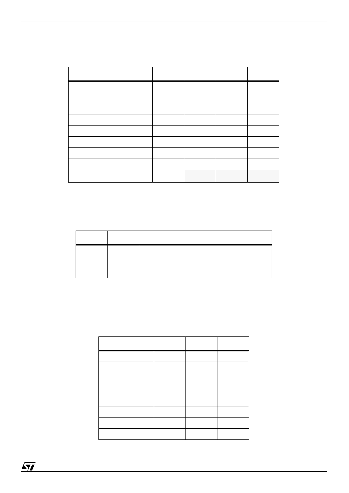
Table 24: Character Background Color
Color BC BR BG BB
Black 1000
Blue 1001
Green 1010
Cyan 1011
Red 1100
Magenta 1101
Yellow 1110
White 1111
Window Backg rou nd Color
1. See Table 25
.
BC TI Background Color
1 X Character Background Color (BR, BG and BB)
0 0 Window Background Color (RGBWi)
0 1 Transparent Background (Video active)
4.5.2 Character Color
A character color can be separat ely pr ogrammed f or each of t he color -bo x e s. This v alu e is select ed
by bits FR, FG and FB.
1
0
Table 25: Background Color Priority
T able 26: Character Colors
Color FR FG FB
Black 000
Blue 001
Green 010
Cyan 011
Red 100
Magenta 1 0 1
Yellow 110
White 111
23/49
Page 24
Character Sp ecifications STV9937
4.5.3 Character Blinking Effect
A character blin king eff ect can be separ ately pr ogrammed fo r each of the color-b o x es . This v alue is
selected by the BLINK bit. When this bit is set to 1, t he b linking effect is enab led and the charact ers
blink.
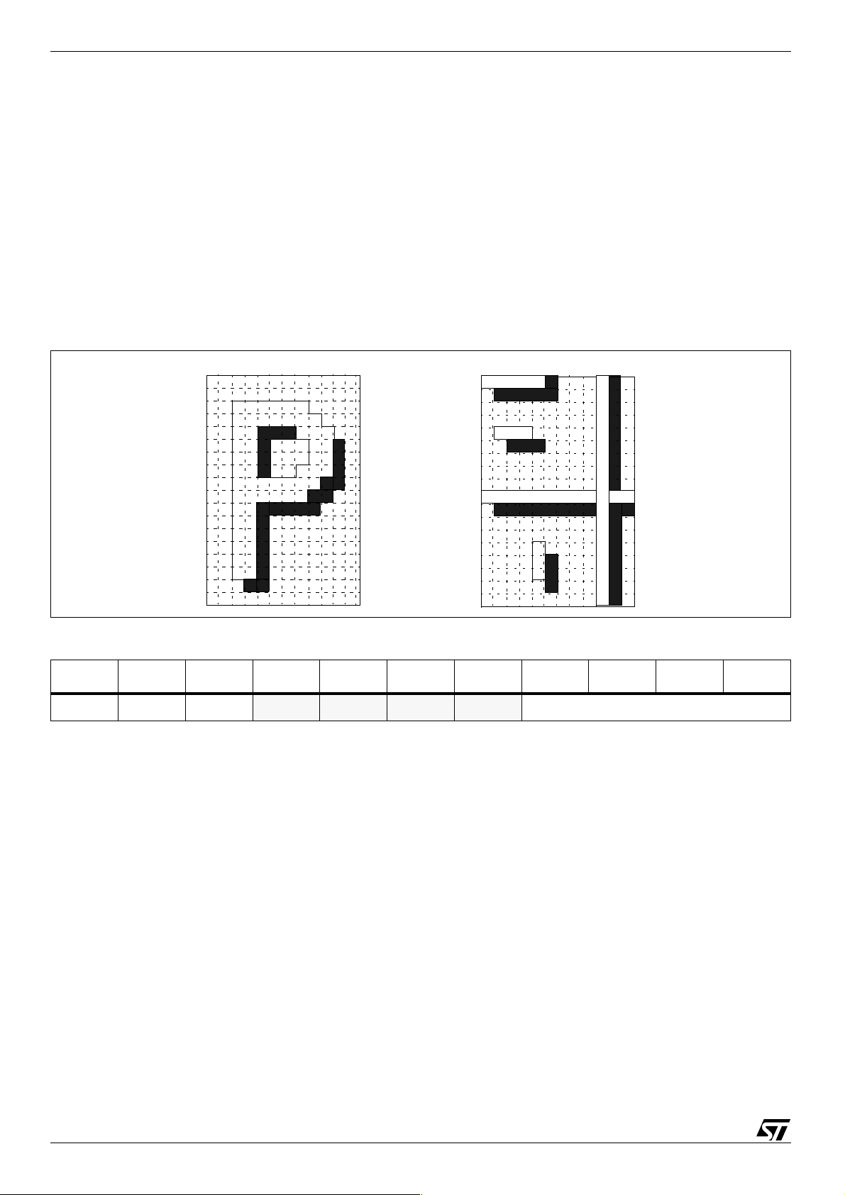
4.6 Character Shadowing
A character shadowi ng effect can be s eparately prog rammed for each of the color- box es. This v alue
is selected by bits CSHA[3:0], respective ly. The shadowing color is black.
When this bit is set to 1, the characters of the corr esponding OSD window are displayed with a
shadowing effect, as shown in Figure 10. The default value is 0 (no shadowing effect).
Figure 10: Character Shadowing
Table 27: Character Shadowing
FWR FAC Default Bit 7 Bit 6 Bit 5 Bit 4 Bit 3 Bit 2 Bit 1 Bit 0
80h 08h 0h CSHA[3:0]
24/49
Page 25
STV9937 Character Specifications
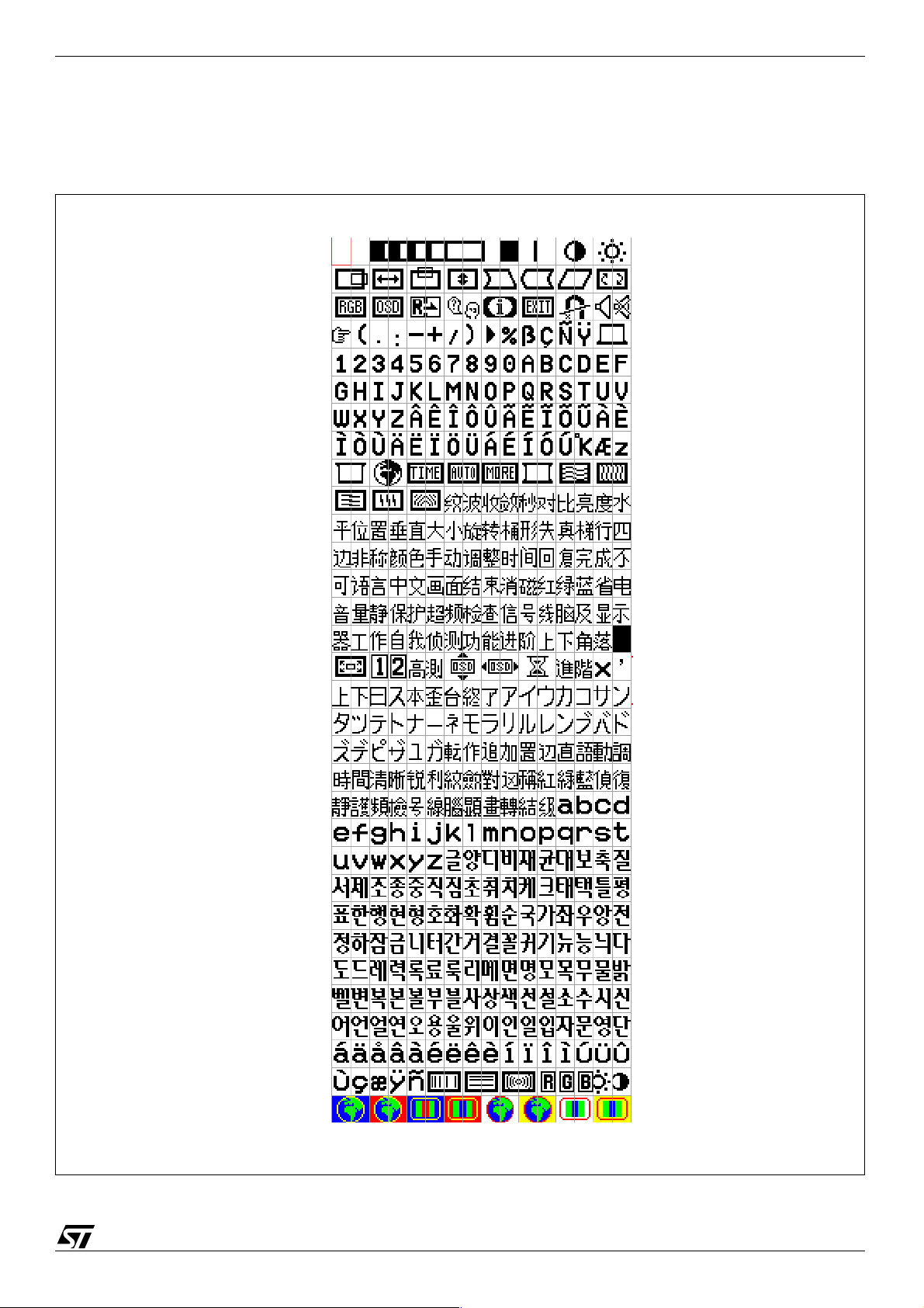
4.7 Character Font
Figure 11 shows the a vailable character font stored in ROM.
Figure 11: Character Fonts
0123456789ABCD
0
1
2
3
4
5
6
7
8
9
A
B
C
D
E
F
EF
10
11
12
13
14
15
16
17
18
19
1A
1B
1C
1D
1E
1F
25/49
Page 26
RAM Specification STV9937
5 RAM Specification
5.1 Character Coding
Each character to display is coded with 12 bits in the RAM with the following addressing method:
● Character Code: Bits RC[8:0] are used to address the ROM Code
● Color Code: Bits CB[2:0] are used to select 1 of the 8 color- boxes in the color shop of the
corresponding OSD window.
Table 28: Character Coding
FWR FAC Bit 11 Bit 10 Bit 9 Bit 8 Bit 7 Bit 6 Bit 5 Bit 4 Bit 3 Bit 2 Bit 1 Bit 0
See Table 3 CB[2:0] RC[8:0]
5.2 Window Memory Allocation
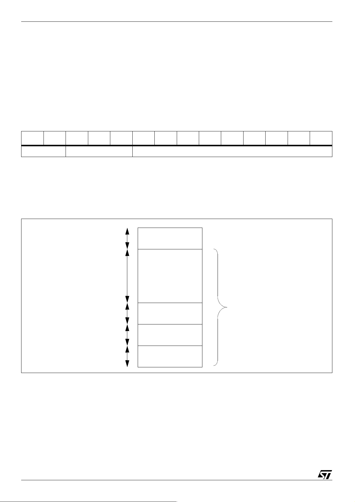
The 4 OSD windows can be distributed differently. But the displayable windows will always contain
a total of 20 blocks ( 1 block consists of 32 characters).
Figure 12: Window Memory Space
1 Block
10 Blocks
4 Blocks
3 Blocks
3 Blocks
Window 0
Color-boxes
Window 1
Window 2
Window 3
Window 4
Displayable
Windows
5.3 Memory Size Allocation
The total number of char acters or spac es is up to 640 with a maximum wi ndow si ze of 16 r ows of 32
characters.
The character codes of each windo w are allo cated to a specific memory space. This memory space
is programmable for each window. The window size must be less than or equal to its memory
allocation. Any windo w size can be modified within its specific memory space, the other windows
are not affected by this operation.
26/49
Page 27
STV9937 RAM Specification
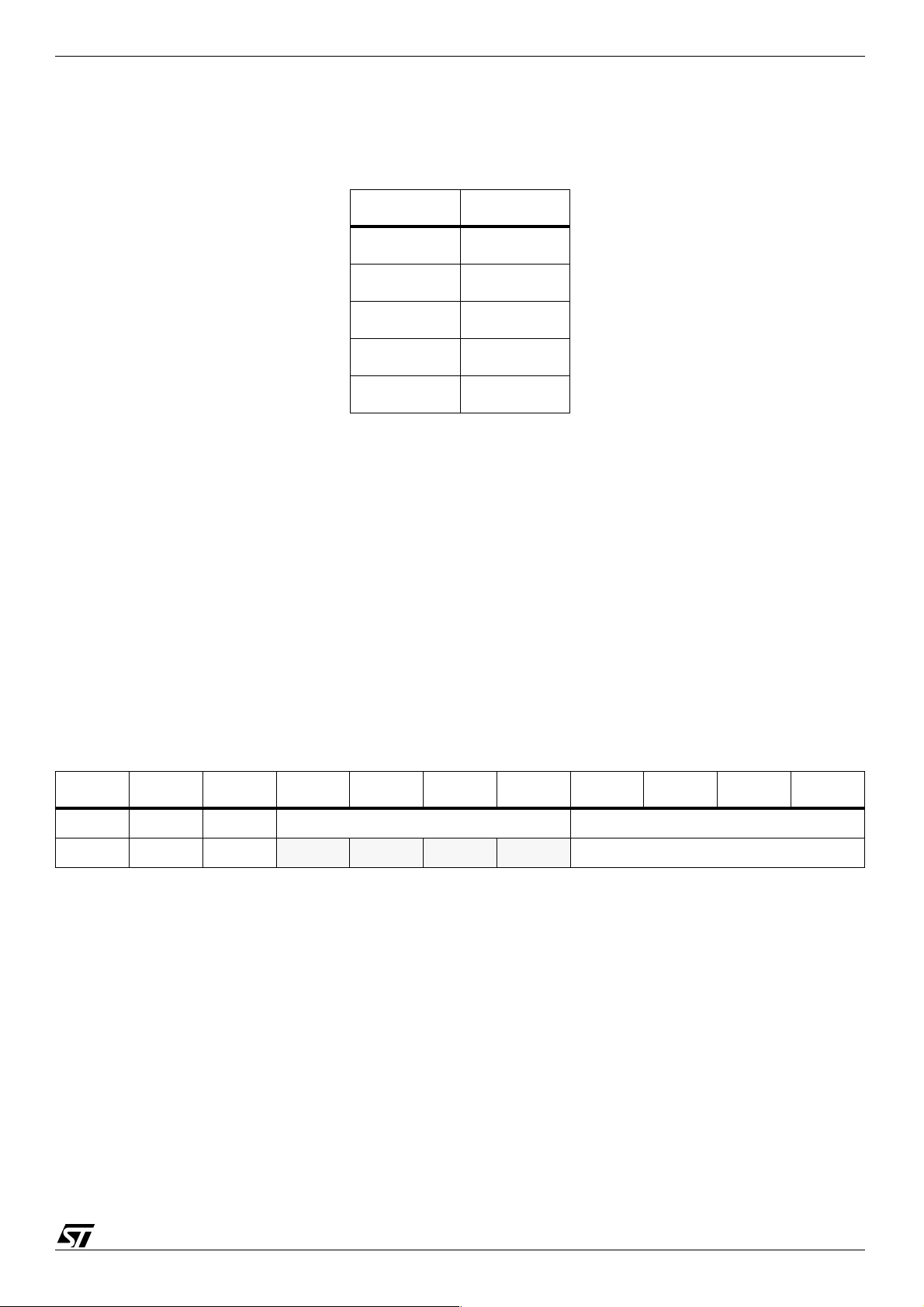
The user must reserve a memory space for the largest window . According to the e xample shown in
Figure 6, the total number of characters/spaces are:
Table 29: Window Sizes
Window Size
Window 1
Window 2
Window 3
Window 4
Total
For e xampl e , t o c hange the si ze of Windo w 3 f rom 3 r o ws of 6 c harac ter s to 5 r ows of 4 c harac ters ,
the resulting size is 20 char acters . The n umber of r ows increa ses and the n umber of charac ters pe r
row decreases. The required memory is at least 20 characters.
Note: A space is considered as being a character.
The memory allocation is made by blocks of 32 char acters.
The maximum size of a windo w is 16 rows of 32 character s , or 512 chara cters . This cor responds to
16 blocks of 32 characters.
1 block is reserved for the color-boxes (see Chapter 4: Character Specifications on page 20),
leaving 20 blocks of 32 characters for character codes (640 characters maximum).
The RAM allocation for each window is coded in bits ALWi[3:0]. Window 4 memory allocati on uses
the remaining memory space.
28
20
18
16
82
Table 30: Window RAM Allocation
FWR FAC Default Bit 7 Bit 6 Bit 5 Bit 4 Bit 3 Bit 2 Bit 1 Bit 0
80h 09h 39h ALW2[3:0] ALW1[3:0]
80h 0Ah 2h ALW3[3:0]
The number of memory blocks allocated for window “i” is (ALWi +1), the range of allocation is 1 to
16 blocks of 32 characters. The total number of blocks is 20.
Note: If the user changes only 1 window allocati on, the RAM a ddresses of t he follo wing wi ndows change.
Consequently we advise you to write the allocation when the windows are not displayed to avoid
false images.
27/49
Page 28
RAM Specification STV9937
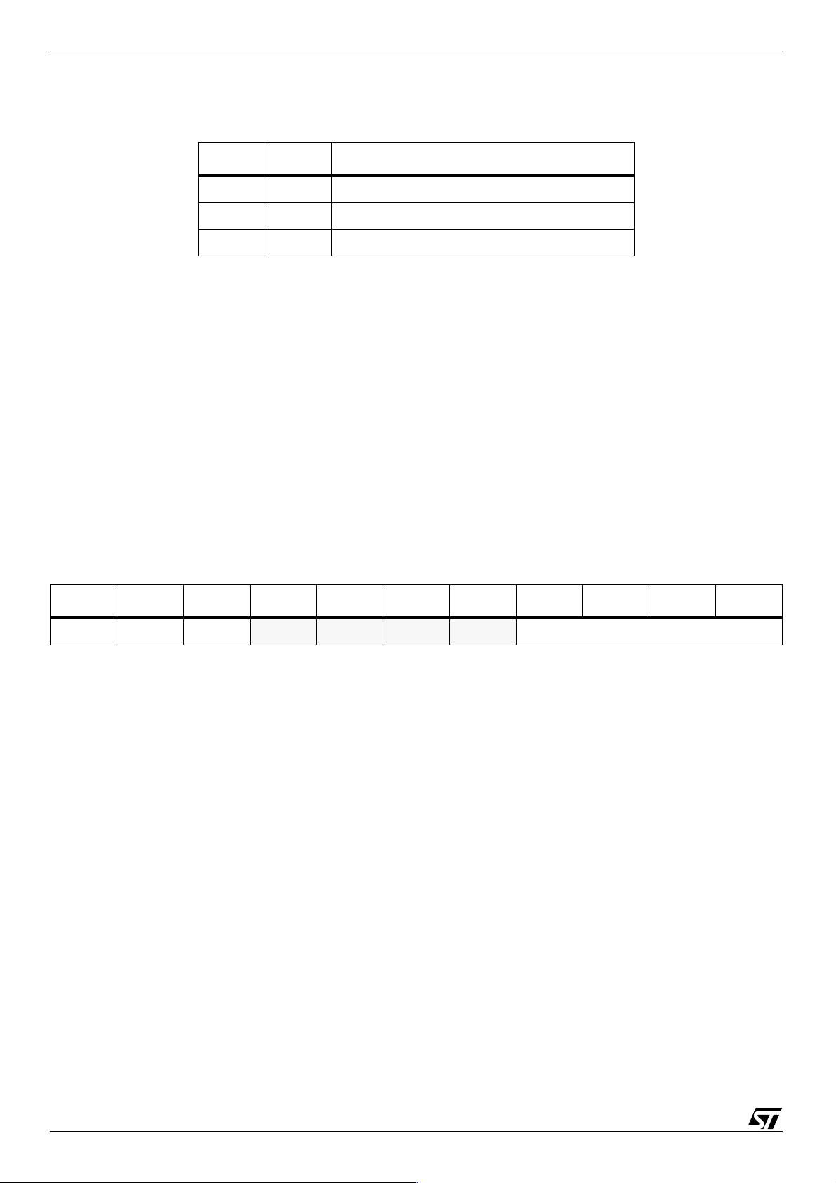
The default window RAM allocations are listed in Table 31.
Table 31: Window RAM Default Values
ALWi Default Description
ALW1 9h 320 Characters (10 blocks)
ALW2 3h 128 Characters (4 blocks)
ALW3 2h 96 Characters (3 blocks)
Window 1: 10 blocks of 32 words = 320 characters (ALW1 = 9).
Window 2: 4 blocks of 32 words = 128 characters (ALW2 = 3).
Window 3: 3 blocks of 32 words = 96 characters (ALW3 = 2).
Window 4: the remaining RAM (3 blocks = 96 characters).
5.4 Window Reset
All the RAM data from one of the four OSD windows can be reset by writing to bits RESETW[3:0].
When the RESETW bit is set to 1, all the RAM data in the allocation memory space of the
corresponding OSD window is reset. These bi ts are automaticall y cleared when the RAM allocatio n
reset is finished.
Table 32: RAM Allocation Enable and Reset
FWR FAC Default Bit 7 Bit 6 Bit 5 Bit 4 Bit 3 Bit 2 Bit 1 Bit 0
80h 0Bh 0h RESETW[3:0]
28/49
Page 29
STV9937 Pixel Clock Generator
6 Pixel Clock Generator
The Pixel Clock Generator is used to synchronize the display clock with the horizontal
synchronisation (Hsync) signal. This generator is based on a PLL function used to perform correct
jitter . The pix el fr equency is defined wit h the horizontal line frequ ency and the horizontal resolut ion.
Pixel Frequency (F
PIXEL2
) = 12 x HR[6:0] x f
HLINE
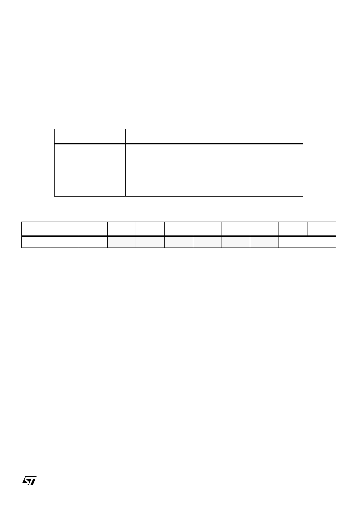
The VCO[1:0] value is used to select the appropriate curve partition of the VCO.
Table 33: VCO Curve Partition
VCO Value (Binary) VCO Curve Partition
00
01
10
11
7.68 MHz < F
MHz < F
15
30 MHz < F
MHz < F
60
PIXEL2
PIXEL2
PIXEL2
< 15 MHz (Default Value)
PIXEL2
< 30 MHz
< 60 MHz
< 120 MHz
Table 34: VCO Range
FWR FAC Default Bit 7 Bit 6 Bit 5 Bit 4 Bit 3 Bit 2 Bit 1 Bit 0
80h 00h 0h VCO[1:0]
The PLL generates:
● a pixel clock for the OSD from 7.68 MHz to 120 MHz: F
● a pixel clock for the PictureBooST
TM
The PictureBooST
pixel clock provides the resolution of the PB pixel.It is locked on the HSYNC
TM
(PB) from 30 to 60 MHz: F
PIXEL2
PIXEL1
.
signal and the referenced edge is programmed using the HSP bit.
When the monitor resolution is changing, the micro cont roller changes the OSD horizontal
resolution to adapt the width of the OSD window. In this case, the frequency of the PB clock is
changing also. So the width and the position and the resolution of the PB windo w is changi ng.
29/49
Page 30
Picture BooSTTM STV9937
7Picture BooST
TM
Picture BooSTTM allows images to be boosted either within a windo w, a screen area or over the
entire screen. To perform this function, the STV9212 preamplifier is required as well as the Picture
BooST
TM
software which sends the window or sc reen area coordina tes (X1, X2,Y1,Y2) to the RGB
video channels.
TM
The Picture BooST
● The RGB Comparator
● The Coordinate Decoder
● The Control and Data registers
system embedded in the STV9937 includes:
The STV9937 computes the data received on the RGB channel and generates a BooST signal
which is then sent to the STV9212. The coordinates can be received through the I²C bus by the
MCU as well.
The STV9937 also includes three 8 bits register used to store data received by RGB.
7.1 Video RGB Input Stage
The input stage is a triple analog-digital buffer for the video RGB inputs.
● The input voltage range is 0 to 0.7 V
● The inputs have to be supplied through a serial capacitor (100nF)
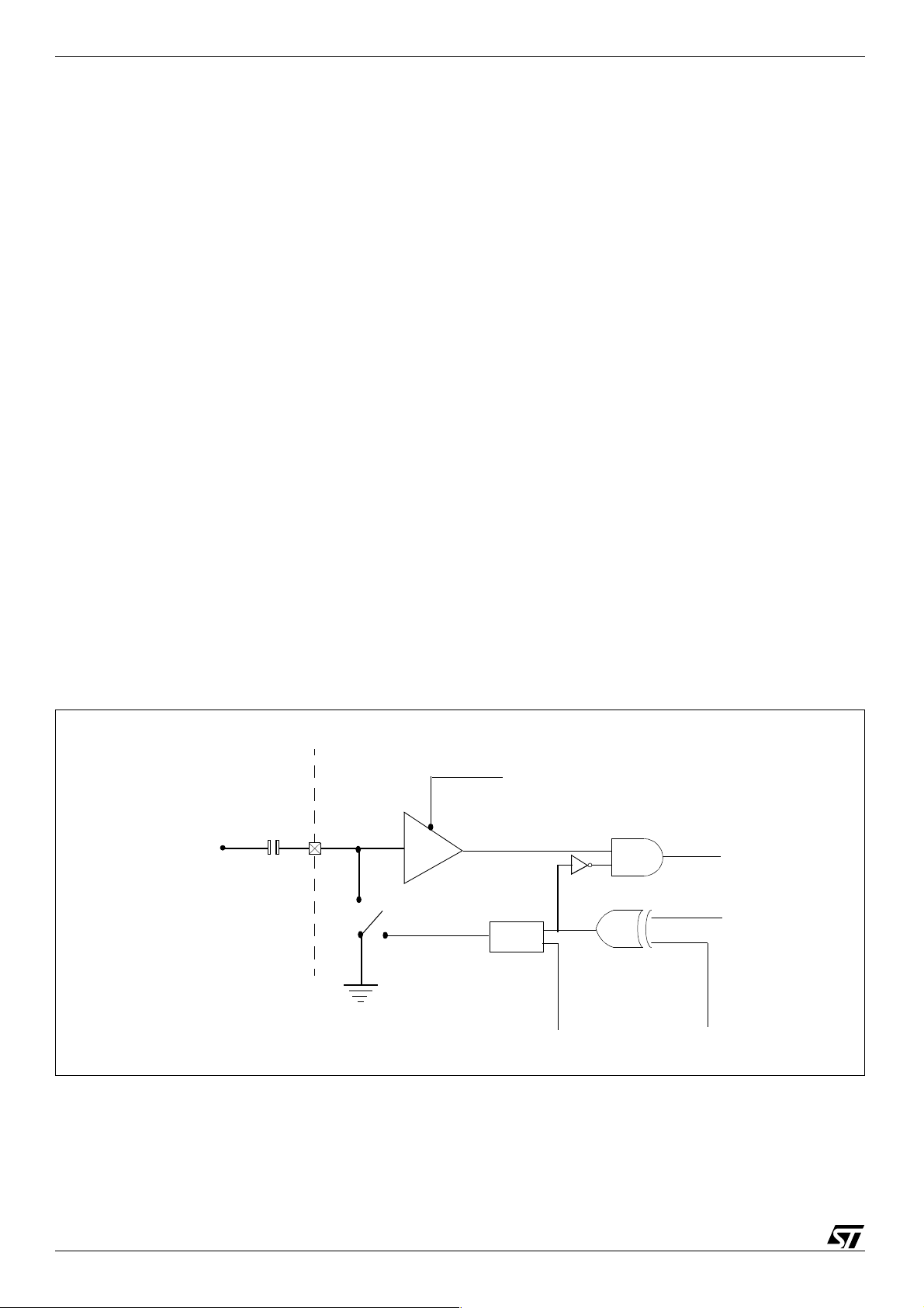
● The input RGB must be set to ‘0’ during the horizontal sync .
The input stage includes a clamping function using the Hsync signal to fix the DC level of inputs.
Figure 13: Hsync Clamping Function
THTCL
100nF
HSYNC
AND
ENCL
CLP
The input stage is configured by thr ee control bits; THCTL, CLP and ENCL as shown in Figure 37.
30/49
Page 31
STV9937 Picture BooSTTM
7.2 PictureBooSTTM RGB Decoder
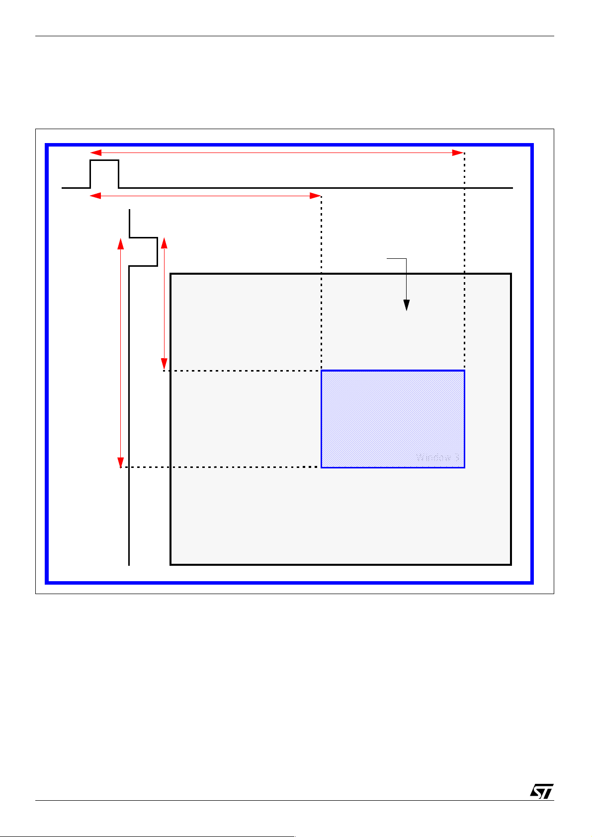
The STV9937 can receive the coordinates of the area to BooST through the RGB channel or
through I²C bus.
TM
The Picture BooST
area coordinates are coded as follows:
Table 35: PictureBooSTTM Window Coordinates
Bits Description
X1[12:0]
X2[12:0] Right coordinate of the window, in CLK1 pixels
Y1[10:0] Top coordinate of the window, in lines
Y2[10:0] Bottom coordinate of the window, in lines
Left coordinate of the window, in CLK1 pixels (F
7.2.1 Data Sent Using I²C
Before sending data to the corresponding registers, the PBVM bit must be set to 1. Then the
coordinates can be sent to the corresponding address, see Table 36:
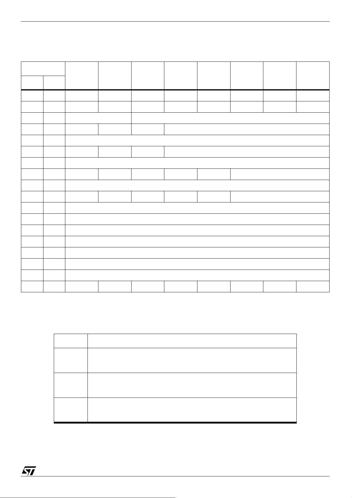
● Row 1, Col 3 to 6 for X1, X2 coordinates
● Row 1, Col 7 to 10 for the Y1, Y2 coordinates.
7.2.2 Data Sent Using the RGB Channel
The Picture BooST
● The Red channel contains the X1, X2 and Y1, Y2 coordinates information
● The Green Channel contains a specific activation code
● The Blue Channel contains the clock signal.
The Decoder stores the coordinates values to the corresponding address:
TM
Software sends coordinate data through the RGB channel:
PIXEL1
)
● Row 1, Col 3 to 6 for X1, X2 coordinates
● Row 1, Col 7 to 10 for the Y1, Y2 coordinates.
X1 and X2 are referred to the HSYNC signal, the resolution is F
(from 30 Mhz to 60 Mhz)
PIXEL1
31/49
Page 32
Picture BooSTTM STV9937
In the same way, 3 other 8 bits of register data(D3A, D3B and D3C)can be sent via the video RGB
and detected by the STV9937. These three register s can be read by the I²C b us at Row1, Col 11 to
13. This specific data cannot be written by I²C.
Figure 14: PictureBoostTM area Coordinates
X
H
SYNC
V
SYNC
2
X
1
Screen
Y
2
Y
1
(X1, Y1)
BOOSTED
AREA
Window 3
(X
, Y2)
2
32/49
Page 33
STV9937 Picture BooSTTM
7.3 Control Registers Descripti on
Table 36: Control Registers PB: Window 0, W[2:0] = “000”, row = 1 R[3:0] =”0001”
Address
Bit 7 Bit 6 Bit 5 Bit 4 Bit 3 Bit 2 Bit 1 Bit 0
Row Col.
1 0 THCTL CLP ENCL HFLYP OSDREF Reserved ENPB
1 1 Reserved Reserved PBVM PBON
1 2 OFFSETLIN[1:0] OFFSETPIX[5:0]
13 X1[12:8]
14 X1[7:0]
15 X2[12:8]
16 X2[7:0]
17 Y1[10:8]
18 Y1[7:0]
19 Y2[10:8]
1A Y2[7:0]
1 B D3A[7:0]
1 C D3B[7:0]
1D D3C[7:0]
1E Reserved
1F Reserved
1 1x Reserved
11FHMUX 0 0 0 0 0 0 0
Table 37: PictureBooSTTM Configuration
Bit Description
The THCTL bit selects the thresholds of the input voltage (low or high)
THCTL
0: Low thresholds selected
1: High thresholds selected (Default value)
CLP
ENCL
The CLP bit selects the polarity of the Hsync signal for the clamp
0: Clamp when Hsync = 1 (Default value)
1: Clamp when Hsync = 0
The ENCL bit enables the clamping function for the RGB input stage
0: Clamping disabled
1: Clamping enabled (Default value)
33/49
Page 34
Picture BooSTTM STV9937
Table 37: PictureBooSTTM Configuration
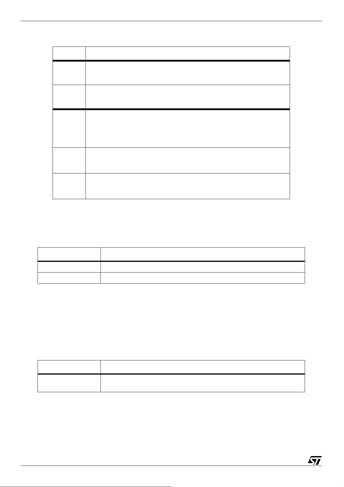
Bit Description
The HFLYP bit configures the polarity of the HFLY signal
HFLYP
OSDREF
0: Falling edge active (default value)
1: Rising edge active
The OSDREF selects the signal taken as reference
0: HFLY is the reference (default value)
1: HSYNC is the reference
The ENPB bit selects Picture BooST
ENPB
PBON
PBVM
0: The RGB video inputs are not decoded, there is no possibility of displaying the PB.
The user can write X1/X2 Y1/Y2 coordinates in the registers, but the On/Off bit is
inactive (default value)
1: PB decoding is active and the PB display can be made active with the PBON bit
The PBON bit selects Picture BooST
0: PB is not displayed (default value)
1: PB is displayed on the screen with the coordinates written in the X/Y registers
The PBVM bit selects the Picture BooST
0: Interface via RGB (default value)
1: Interface via I²C
7.4 Line and Pixel Offsets
Due to the intrinsic del ay on the RGB channel during the RGB decodi ng, 2 offsets can be applied for
fine tuning as shown in below:
Bits Description
OFFSETLIN[1:0] The line offset in SIGNED radix is coded on 2 bits from -2 to +1. Default value is 0.
OFFSETPIX[5:0] The pixel offset in SIGNED radix is coded on 6 bits from -32 to +31. Default value is 0.
TM
decoding
TM
display
TM
interface
Note:It is recommended to adjust the pixel offset each time the monitor resolution changes.
7.5 PLL Synchronised
The STV9937 PLL can either be synchronized on the HFLY or HSYNC signals.
WARNING:Once synchronized on HFLY, the Picture BooST
Bit Description
HMUX
34/49
0: HSYNC is the synchronization signal
1: HFLY is the synchronization signal
TM
feature cannot be guaranteed.
Page 35
STV9937 General OSD Programming
8 General OSD Programming
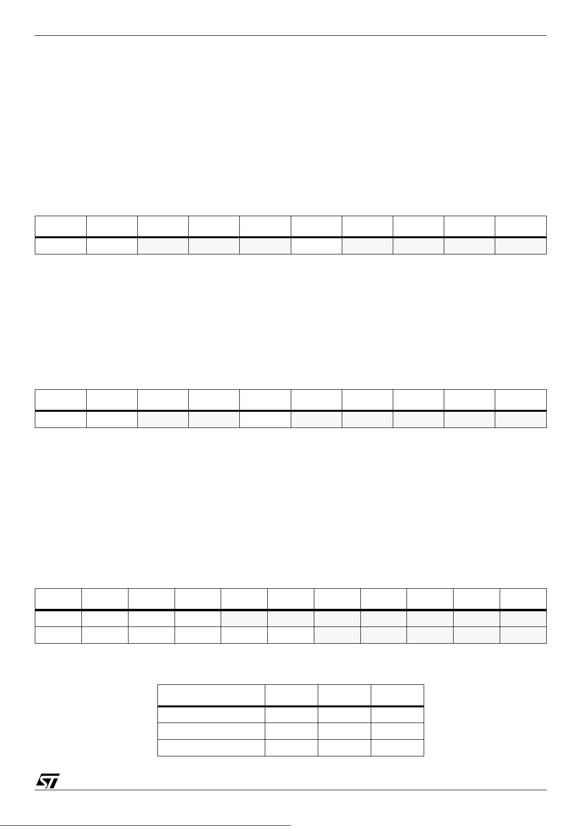
8.1 Enable OSD
The OSD window displays are enabled by the ENOSD bit.
ENOSD = 1: OSD window displays are active.
ENOSD = 0: OSD window displays are inactive. Pin FBLK = 0 and pins ROUT, GOUT and
BOUT pins = 0 (bit RGBPOL is 0). The default value is 0.
Table 38: Enable OSD
FWR FAC Bit 7 Bit 6 Bit 5 Bit 4 Bit 3 Bit 2 Bit 1 Bit 0
80h 00h ENOSD
8.2 Fade-in and Fade-out Effect
The Fade-i n and Fade-out effect is used to progressively increase/decrease the OSD window to/
from its full size. This effect is enabled by the FADE bit.
FADE = 1: Fade effect is active
FADE = 0: Fade effect is inactive (default value)
Table 39: Fade
FWR FAC Bit 7 Bit 6 Bit 5 Bit 4 Bit 3 Bit 2 Bit 1 Bit 0
80h 00h FADE
8.3 Full Screen Display
The STV9937 allows a full screen display with a selectable color programmable by the FBK bit as
follows:
FBK = 1: The video area is repl aced by the color coded i n bits FSR, FSG and FSB (full screen
color values). Pin FBLK is always 1.
FBK = 0: Normal video mode whether or not the OSD menu is displayed. The default value of
bit FBK is 0.
T a ble 40: Full Screen Registers
FWR FAC Default Bit 7 Bit 6 Bit 5 Bit 4 Bit 3 Bit 2 Bit 1 Bit 0
80h 01h 0h FBK
80h 03h 0h FSR FSG FSB
T able 41: Full Screen Colors
Color FSR FSG FSB
Black (Default Value) 0 0 0
Blue 001
Green 010
35/49
Page 36
General OSD Programming STV9937
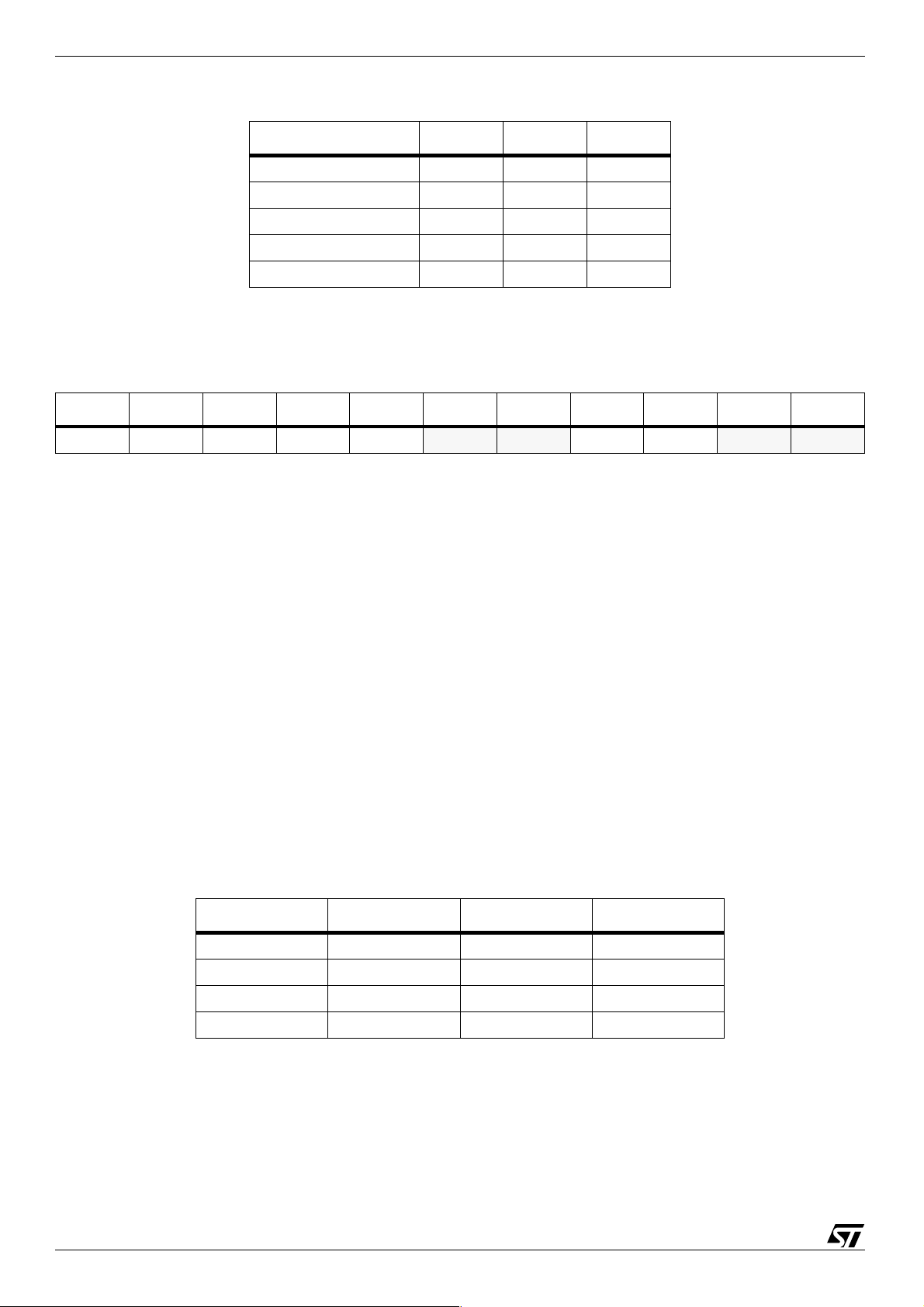
Table 41: Full Screen Colors (Continued)
Color FSR FSG FSB
Cyan 011
Red 100
Magenta 1 0 1
Yellow 110
White 111
8.4 Signal Polarity and Triggering
Table 42: Signal Polarity
FWR FAC Default Bit 7 Bit 6 Bit 5 Bit 4 Bit 3 Bit 2 Bit 1 Bit 0
80 00 FBKPOL RGBPOL VSP HSP
V ertical Sync Triggering (VS input)
The active edge of the VS pin used for vertical synchronization is selected by bit VSP.
VSP = 0: The falling edge is active. (Default Value)
VSP = 1: The rising edge is active.
Horizontal Sync Triggering (HSYNC input)
The active edge of the HSYNC pin used for horizontal synchronization is selected by bit HSP.
HSP = 0: The falling edge is active . (Default Value)
HSP = 1: The rising edge is active.
RGB Output Polarity (ROUT, GOUT and BOUT outputs)
The output polarity of pins ROUT, GOUT and BOUT is selected by bit RGBPOL.
RGBPOL = 0: RGB active at 1 (Default Value)
RGBPOL = 1: RGB active at 0
Table 43: RGB Output Control
ENOSD Bit RGBPOL Bit RGB Outputs Display
1 0 Active at 1 OSD
1 1 Active at 0 OSD
00000Video
01111Video
36/49
Page 37
STV9937 General OSD Programming
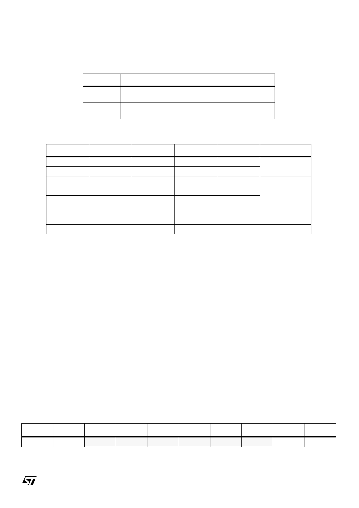
Fast Blanking Output Polarity (FBLK output)
The output polarity of the FBLK pin is selected by bit FBLKPOL. The default value is 0.
Table 44: Fast Blanking Output Polarity Selection
FBLKPOL Description
ENOSD Bit FBLKPOL Bit FBK Bit FBLK Output Display
1000Video
1001OSD
1011OSDFull Screen
1100OSD
1101Video
1110OSDFull Screen
0 0 x 0 Video No OSD
0 1 x 1 Video No OSD
8.5 Reset
0
1
When OSD display, FBLK = 1
When active video, FBLK = 0
When OSD display, FBLK = 0
When active video, FBLK = 1
Table 45: FBLK Output Control
Default Value
FBLK Inverted
Power On Reset
The digital core and the PLL are asynchronously reset at Power On.
Soft Reset
A soft reset is enabled by the RST bit.
TM
RST = 1: The digital core is reset. All control registers including PictureBooST
but with the
exception of PLL registers, are reset at the same value as at power on reset.
It is not necessary to write RST = 0 to stop the reset. This bit is automatically cleared.
PLL Register Reset
The Pixel Clock Generator (VCO[1:0]) and Horizontal Resolution (HR[6:0]) bits are reset by the
RST_PLL bit.
RST_PLL = 1: HR[6:0] and VCO[1:0] are reset to the same value as the power-on reset.
It is not necessary to write RST_PLL = 0 to stop the reset. This bit is automatically cleared.
Table 46: Reset
FWR FAC Bit 7 Bit 6 Bit 5 Bit 4 Bit 3 Bit 2 Bit 1 Bit 0
80h 06h RST_PLL RST
37/49
Page 38
Registers STV9937
9Registers
9.1 Register Specification
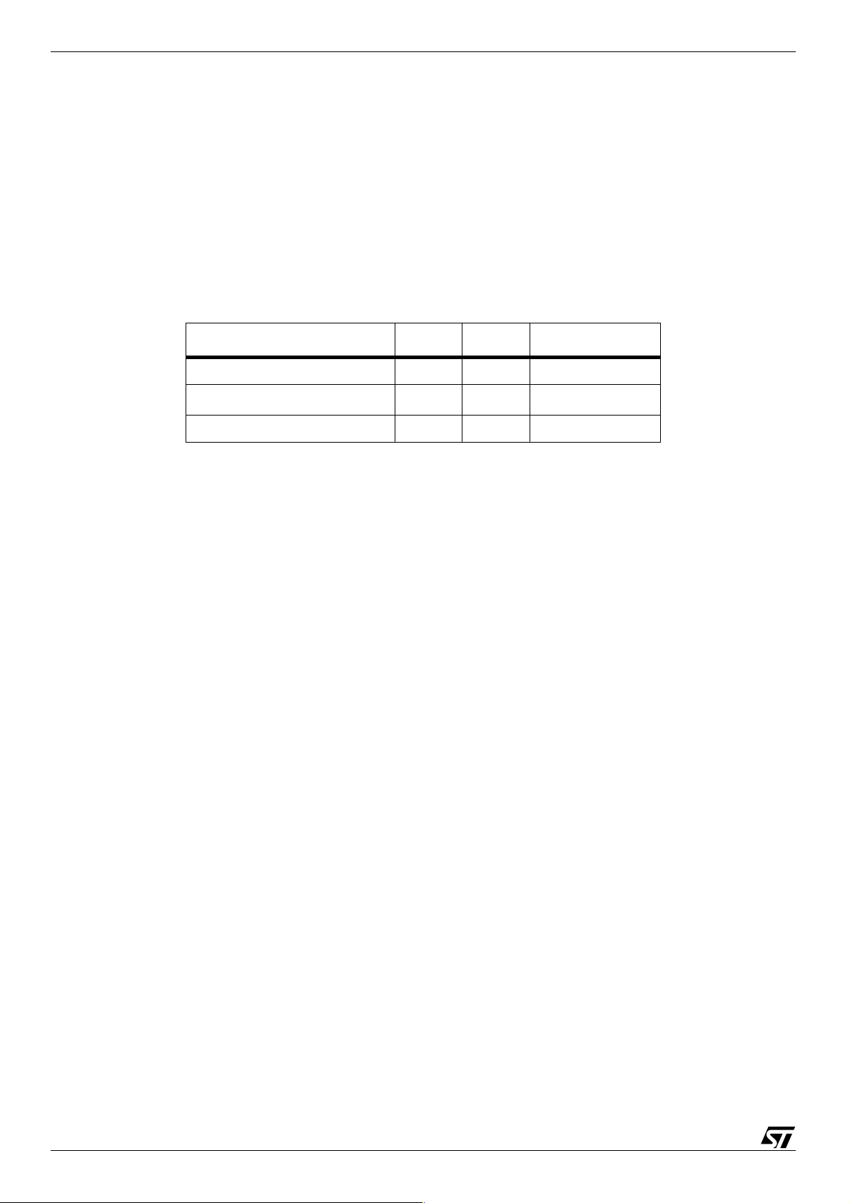
Control registers are located at address in Window 0, Row 0 and Row 1.
Color-boxes are located at addresses in Window 0, Row 2. See Section 4.5 on page 22.
Character codes are located at addresses in Windows 1 to 4, as described in Section 5.1 on
page 26.
Table 47: Non-Displayable Window Register Mapping
Register Window Row FWR Code
OSD Control Registers 0 0 80h
PictureBooST
Color-box Registers 0 2 82h
TM
Control Registers
0 1 81h
38/49
Page 39
STV9937 Registers
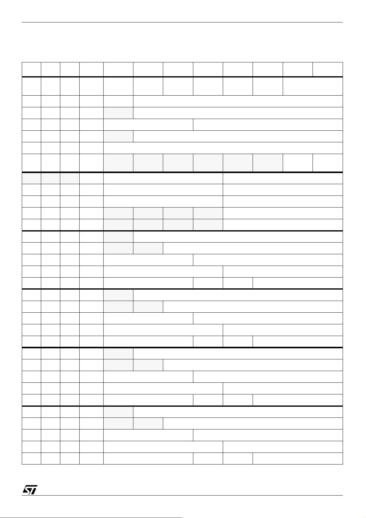
Table 48: Control Registers: Window 0, Row = 0
FWR FAC Col Default Bit 7 Bit 6 Bit 5 Bit 4 Bit 3 Bit 2 Bit 1 Bit 0
80h 00h 0h 0h
80h 01h 1h 20h FBK = 0 HR[6:0] :Horizontal Resolution = 32 characters
80h 02h 2h 12h
80h 03h 3h 0h full screen RGB = FS RGB = 000 RSPA[4:0] = Row Spacing = 0
80h 04h 4h 0h
80h 05h 5h 0h VD[7:0] = Vertical Delay Reference = 0 (2 lines)
80h 06h 6h 0h
80h 07h 7h 0h ENBS4/3/2/1 = 0000 ENW4/3/2/1 = 0000
80h 08h 8h 0h CSHA[3:0] = 0
80h 09h 9h 39h ALW2[3:0] = 3 (4 blocks = 128 characters) ALW1[3:0] = 9 (10 blocks = 320 characters)
80h 0Ah Ah 2h
80h 0Bh Bh 0h
80h 0Ch Ch 0h HDW1[6:0] = 0
80h 0Dh Dh 0h
80h 0Eh Eh 19h BSWW1[2:0] = 000 HSW1[4:0] = 25 (26 characters)
FBKPOL = 0RGBPOL
= 0
F ADE = 0
HD[6:0] = Horizontal Delay Reference = 0 (50 pixels)
ENOSD =
0
CH[6:0] = Character Height = 18
VSP = 0 HSP = 0 VCO[1:0] = 00
ALW3[3:0] = 2 (3 blocks, 96 characters)
RESETW[3:0] = 0000
VDW1[5:0] = 0
RST_PLL
= 0
RST = 0
80h 0Fh Fh Bh BSHW1[3:0] = 0000 VSW1[3:0] = 11 (12 rows of characters)
80h 10h 10h 7h WS RGB 1 = 000 : black BSW1=0 T1 = 0 RGB W1 = 111:white
80h 11h 11h 20h
80h 12h 12h 0h VDW2[5:0] = 0
80h 13h 13h 9h BSWW2[2:0] = 000 HSW2[4:0] = 9 (10 characters)
80h 14h 14h 4h BSHW2[3:0] = 0000 VSW2[3:0] =4 (5 rows of characters)
80h 15h 15h 7h WS RGB 2 = 000 : black BSW2=0 T2 = 0 RGB W2 = 111:white
80h 16h 16h 0h
80h 17h 17h Ch
80h 18h 18h Fh BSWW3[2:0] = 000 HSW3[4:0] = 15 (16 characters)
80h 19h 19h 7h BSHW3[3:0] = 0000 VSW3[3:0] = 7 (8 rows of characters)
80h 1Ah 1Ah 7h WS RGB 3 = 000 : black BSW3=0 T3 = 0 RGB W3 = 111:white
80h 1Bh 1Bh 10h
80h 1Ch 1Ch Ch
80h 1Dh 1Dh Fh BSWW4[2:0] = 000 HSW4[4:0] = 15 (16 characters)
80h 1Eh 1Eh 7h BSHW4[3:0] = 0000 VSW4[3:0] = 7 (8 rows of characters)
HDW2[6:0] = 32
HDW3[6:0] = 0
VDW3[5:0] =12
HDW4[6:0] = 16
VDW4[5:0] = 12
80h 1Fh 1Fh 7h WS RGB 4 = 000 : black BSW4=0 T4 = 0 RGB W4 = 111:white
39/49
Page 40
Registers STV9937
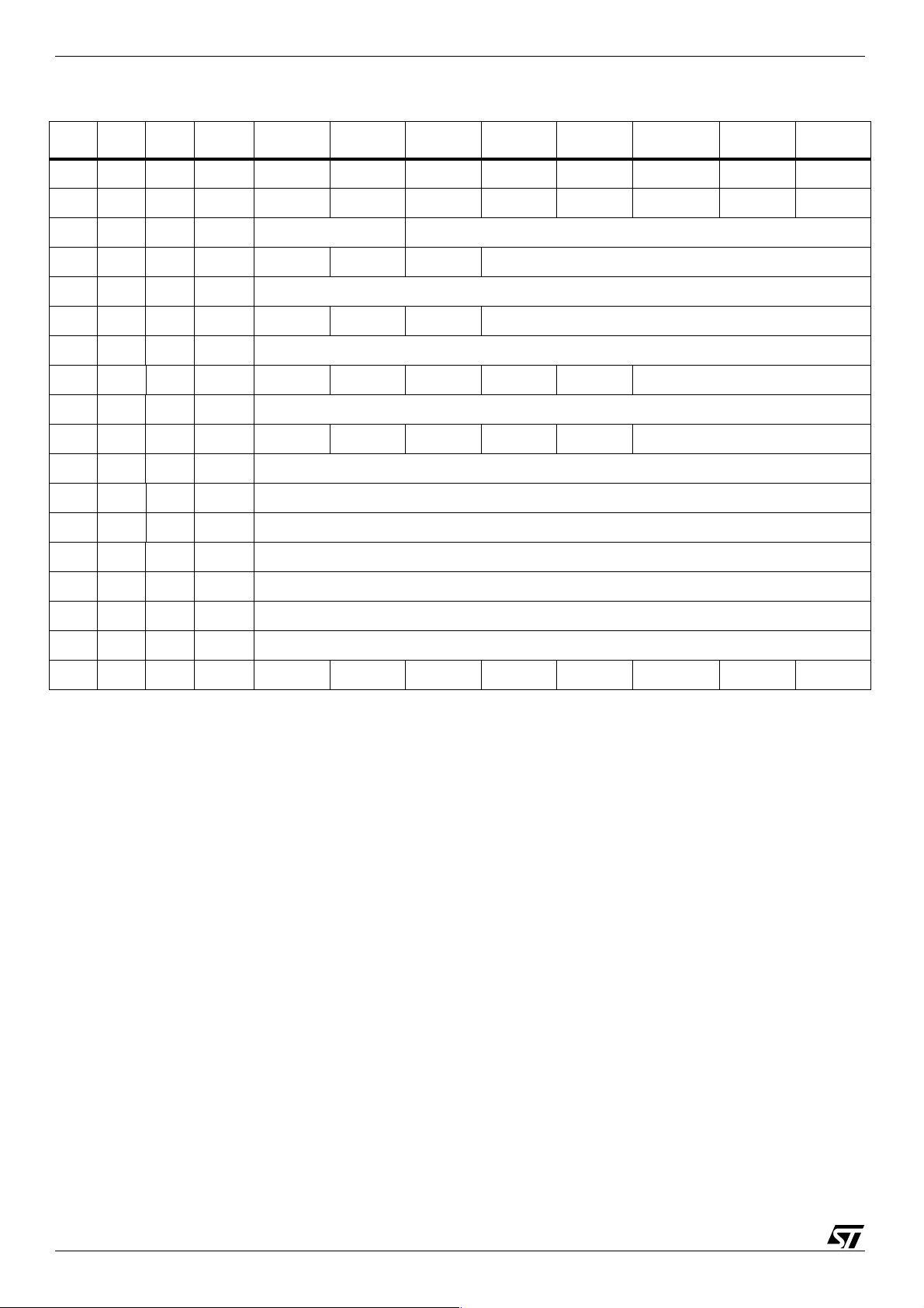
Table 49: Control Registers: Window 0, Row = 1
FWR FAC Col Default B it 7 Bit 6 Bit 5 Bit 4 Bit 3 Bit 2 Bit 1 Bit 0
81h 00h 0h 50h 0 THCTL = 1 CLP = 0 ENCL = 1 HFLYP = 0 OSDREF = 0 0 ENPB = 0
81h 01h 1h 4h 0 1 PBVM = 0 PBON = 0
81h 02h 2h 0h OFFSETLIN[1:0] OFFSETPIX[5:0]
81h 03h 3h 0h X1[12:8]
81h 04h 4h 0h X1[7:0]
81h 05h 5h 0h X2[12:8]
81h 06h 6h 0h X2[7:0]
81h 07h 7h 0h Y1[10:8]
81h 08h 8h 0h Y1[7:0]
81h 09h 9h 0h Y2[10:8]
81h 0Ah Ah 0h Y2[7:0]
81h 0Bh Bh 0h D3A[7:0]
81h 0Ch Ch 0h D3B[7:0]
81h 0Dh Dh 0h D3C[7:0]
81h 0Eh Eh 0h Reserved
81h 0Fh Fh 0h Reser ved
81h 1xh 1xh 0h Reserved
81h 1Fh 1Fh 0h HMUX = 0 0 0 0 0 0 0 0
40/49
Page 41
STV9937 Registers
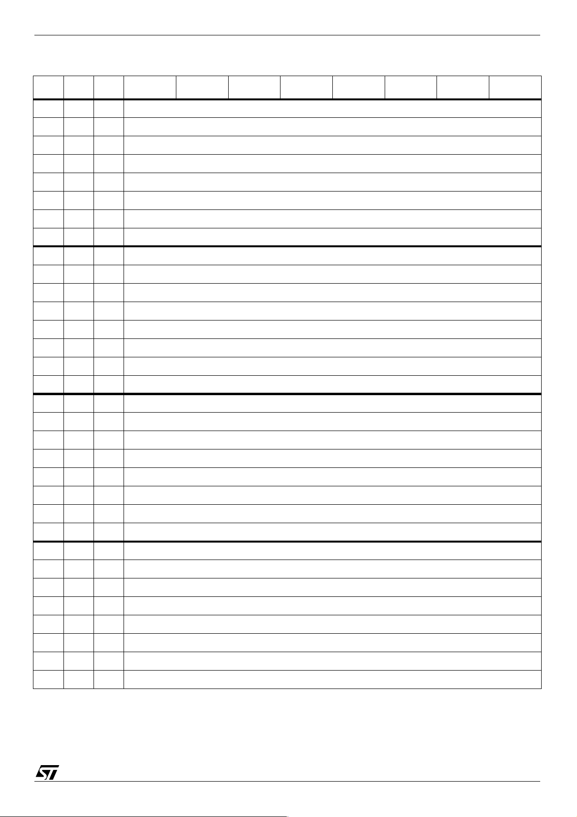
Table 50: Color Registers: Window 0, Row = 2
FWR FAC Col Bit 7 Bit 6 Bit 5 Bit 4 Bit 3 Bit 2 Bit 1 Bit 0
82h 00h 0h WINDOW1 Color-box 1: BC- BR-BG-BB-blink-FR-FG-FB
82h 01h 1h WINDOW1 Color-box 2: BC- BR-BG-BB-blink-FR-FG-FB
82h 02h 2h WINDOW1 Color-box 3: BC- BR-BG-BB-blink-FR-FG-FB
82h 03h 3h WINDOW1 Color-box 4: BC- BR-BG-BB-blink-FR-FG-FB
82h 04h 4h WINDOW1 Color-box 5: BC- BR-BG-BB-blink-FR-FG-FB
82h 05h 5h WINDOW1 Color-box 6: BC- BR-BG-BB-blink-FR-FG-FB
82h 06h 6h WINDOW1 Color-box 7: BC- BR-BG-BB-blink-FR-FG-FB
82h 07h 7h WINDOW1 Color-box 8: BC- BR-BG-BB-blink-FR-FG-FB
82h 08h 8h WINDOW2 Color-box 1: BC- BR-BG-BB-blink-FR-FG-FB
82h 09h 9h WINDOW2 Color-box 2: BC- BR-BG-BB-blink-FR-FG-FB
82h 1Ah Ah WINDOW2 Color-box 3: BC- BR-BG-BB-blink-FR-FG-FB
82h 1Bh Bh WINDOW2 Color-box 4: BC- BR-BG-BB-blink-FR-FG-FB
82h 1Ch Ch WINDOW2 Color-box 5: BC- BR-BG-BB-blink-FR-FG-FB
82h 1Dh Dh WINDOW2 Color-box 6: BC- BR-BG-BB-blink-FR-FG-FB
82h 1Eh Eh WINDOW2 Color-box 7: BC- BR-BG-BB-blink-FR-FG-FB
82h 1Fh Fh WINDOW2 Color-box 8: BC- BR-BG-BB-blink-FR-FG-FB
82h 10h 10h WINDOW3 Color-box 1: BC- BR-BG-BB-blink-FR-FG-FB
82h 11h 11h WINDOW3 Color-box 2: BC- BR-BG-BB-blink-FR-FG-FB
82h 12h 12h WINDOW3 Color-box 3: BC- BR-BG-BB-blink-FR-FG-FB
82h 13h 13h WINDOW3 Color-box 4: BC- BR-BG-BB-blink-FR-FG-FB
82h 14h 14h WINDOW3 Color-box 5: BC- BR-BG-BB-blink-FR-FG-FB
82h 15h 15h WINDOW3 Color-box 6: BC- BR-BG-BB-blink-FR-FG-FB
82h 16h 16h WINDOW3 Color-box 7: BC- BR-BG-BB-blink-FR-FG-FB
82h 17h 17h WINDOW3 Color-box 8: BC- BR-BG-BB-blink-FR-FG-FB
82h 18h 18h WINDOW4 Color-box 1: BC- BR-BG-BB-blink-FR-FG-FB
82h 19h 19h WINDOW4 Color-box 2: BC- BR-BG-BB-blink-FR-FG-FB
82h 1Ah 1Ah WINDOW4 Color-box 3: BC- BR-BG-BB-blink-FR-FG-FB
82h 1Bh 1Bh WINDOW4 Color-box 4: BC- BR-BG-BB-blink-FR-FG-FB
82h 1Ch 1Ch WINDOW4 Color-box 5: BC- BR-BG-BB-blink-FR-FG-FB
82h 1Dh 1Dh WINDOW4 Color-box 6: BC- BR-BG-BB-blink-FR-FG-FB
82h 1Eh 1Eh WINDOW4 Color-box 7: BC- BR-BG-BB-blink-FR-FG-FB
82h 1Fh 1Fh WINDOW4 Color-box 8: BC- BR-BG-BB-blink-FR-FG-FB
41/49
Page 42

Application Hints STV9937
10 Application Hints
10.1 Software Hints
10.1.1 Programming Recommendations
1. Write a new allocation just befor e the RAM re set.
2. Write a new allocation at any time but take care of the window display.
3. When resetting the RAM and writing in it just after , write in the RAM respecting the same order
as the reset: from the first to the last reset window, from the first window address (r o w 0, col 0)
to the last, incrementing columns, then row s, then windows.
4. Define the window horizontal size prior to writing character and color codes in RAM.
HSWI is used to compute the RAM address.
10.1.2 Examples of Programming
It is recommended to program the STV9937 in the following sequence:
● Via RGB Video mode
➺ set ENPB =1
➺ send data via RGB Video: Y then X coordinates.
● Via I2C mode
➺ set ENPB =1, PBVM=1, PBON =0
➺ send data via I2C: X and Y coordinates.
➺ set PBON =1
● Changing the mode
➺ set PBON = 0
➺ change PBVM bit
➺ write new coordinates, then the PBON can be set to 1.
Hard reset at power-up (following a power-up)
1. Write Window 0 registers to set the OSD parameters: write
➺ VCO[1:0], horizontal resolution and vertical height of characters,
➺ the position of reference,
➺ the allocations if they are incorrect
(by default: 320 charac ters for window 1, 128 characters for each of the other s windows)
➺ the windows position and size,
➺ the color-boxes that will be used.
2. Write the character codes for each window to display.
3. Write the color-box data for each window to display.
4. Write the enable of windows: ENWi = 1 then ENOSD=1.
Change of position & size of 1 window (ex. window 3) without disable of window
1. Write new position and sizes.
2. Write new characters in the RAM.
42/49
Page 43

STV9937 Application Hints
Re-allocation, reset, and writing new characters in windows
1. Disable windows.
2. Write new allocations .
3. Reset the windows.
4. Write new positions and sizes in control registers.
5. Write new color-boxes.
6. Write new characters and color-box data.
7. Enable windows.
10.2 Hardware Hints
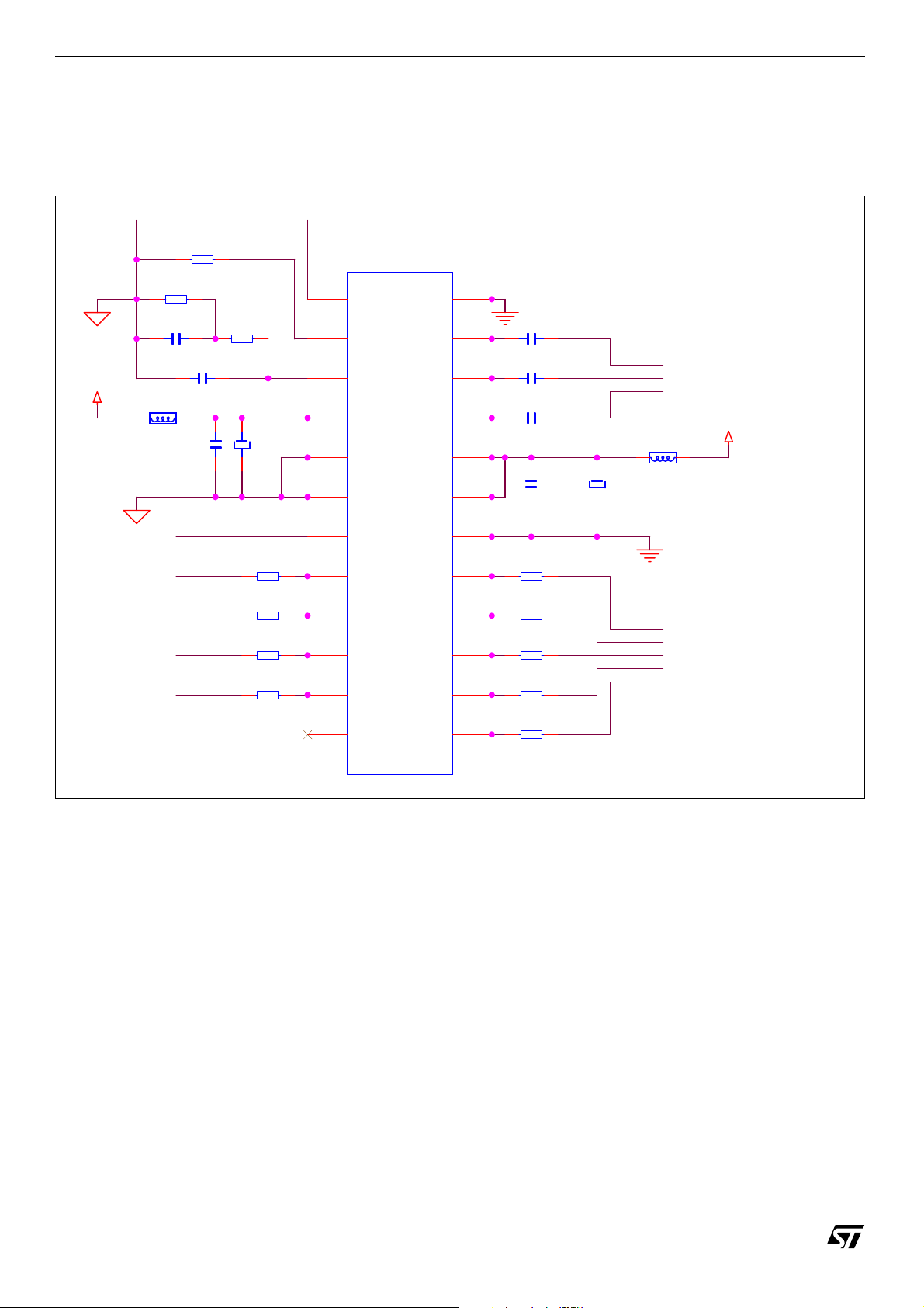
● The serial resistors on the ROUT, GOUT, BOUT, FBLK and PB outputs must be as close as
possible to the device.
● Both decoupling capacitors (100 nF and 100 µF) must be as close as possible to the analog
(pin 13) and digital (pin5) pow er supplies (see Figure 15).
● PLL network must be close to the devi ce but far from the ROUT, GOUT, BOUT, FBLK and PB
outputs. PLL network and ROUT, GOUT, BOUT and FBLK outputs should be separated by the
AVDD 3.3 V power trace.
● PLL ground (AGND) should not be connected either to DVSS or to other grounds of the
videoboard, as the ground is already connect ed int e rnally.
● It is better to supply the STV9937 device through ferrite beads (as an example the ferrite bead
could be 742 760 5 type from Würth Electronik) instead of traditional inductance that could
damage the OSD jitter with some parasitic resonance.
43/49
Page 44
Application Diagrams STV9937
11 Application Diagrams
Figure 15: STV9937 Application Diagram
R35 9K1
U3
3.3V
FB1 BEAD_COIL
R3 3M3
C30 560pF
C1 47pF
100nF
R38 68K
C35
100uF/25V
1
2
3
4
5
6
AVSS
RP
VCO
AVDD
TEST 1
TEST 2
IVSS
BIN
GIN
RIN
IVDD
DVDD
24
23
22
21
20
19
C32 100nF
C33 100nF
C38 100nFC34
C36
100nF
FB2
BEAD_COIL
C37
100uF/25V
From v ideo connector
3.3V
BLK/Hfly
VS
HS
SDA
SCL
R37 100R
R39 100R
R32 100R
R34 100R
7
8
9
10
11
12
HFLY
VS
HSYNC
SDA
SCL
nc
STV9937
DVSS
PB
BOUT
GOUT
ROUT
FBLK
18
17
16
15
14
13
R40 330R
R42 330R
R43 330R
R46 330R
R41 330R
To the pre-amplifier
44/49
Page 45
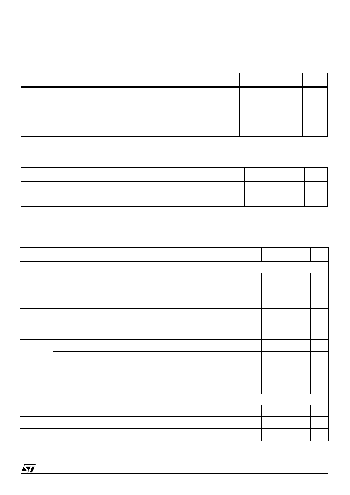
STV9937 Electrical and Timing Characteristics
12 Electrical and Timing Characte r is tics
12.1 Absolute Maximum Ratings
Symbol Parameter Value Unit
AVDD, IVDD, DVDD, OV
V
IN
T
OPER
T
STG
DC Supply Voltage -0.5, +4.0 V
DD
Input Voltage for SCL, SDA, VS, HFLY and HSYNC -0.5, 5.5 V
Ambient Operating Temperature 0, +70
Storage Temperature -40, +125
12.2 Operating Conditions
Symbol Parameter Min. Typ. Max. Unit
VDD
T
OPER
DC Supply Voltage AV
Ambient Operating Temperature 0 25 70
, IVDD, DVDD, OV
DD
DD.
3.0 3.3 3.6 V
12.3 Electrical and Timing Characteristics
(V
= 3.3V, VSS = 0V, TA = 0 to 70o, unless otherwise specified)
DD
Symbol Parameter Min. Typ. Max. Unit
o
C
o
C
o
C
Electrical Characteris tics
IDD
Analog and Digital Supply Current AIDD+ DIDD + OI
DD
50 mA
Input Low Voltage (SCL, SDA, VS, HFLY, HSYNC, TEST1 and TEST2 pins) 0.8 V
V
IL
RIN, GIN, BIN (Video Input Voltage Amplitude)
Input High Voltage (SCL, SDA, VS, HFLY and HSYNC pins)
V
IH
Test inputs are connected to ground
RIN, GIN, BIN (Video Input Voltage Amplitude)
ROUT, GOUT, BOUT, FBLK and PB Output Low Voltage (IOL = 3 mA)
V
OL
SDA Open Drain Output Low Voltage (I
OL
ROUT, GOUT, BOUT, FBLK and PB Output High Voltage (IOH = 3 mA)
V
OH
SDA Open Drain Output High Voltage,
pulled up by external 3V to 5V power supply
1
1
= 4 mA)
050mV
2.0 5.0 V
0.5 0.7 1.0 V
0.4 V
0.4 V
2.4 - V
5.0 V
Timing Characteristics
Freq (Hline) Horizontal Synchronization Inpu t Range 150 kHz
t
r
t
f
ROUT, GOUT, BOUT, FBLK and PB Output rise time (C
ROUT, GOUT, BOUT, FBLK and PB Output fall time (C
LOAD
LOAD
= 15 pF)
= 15 pF)
2ns
2ns
1. For PictureBoost data transmission only
45/49
Page 46
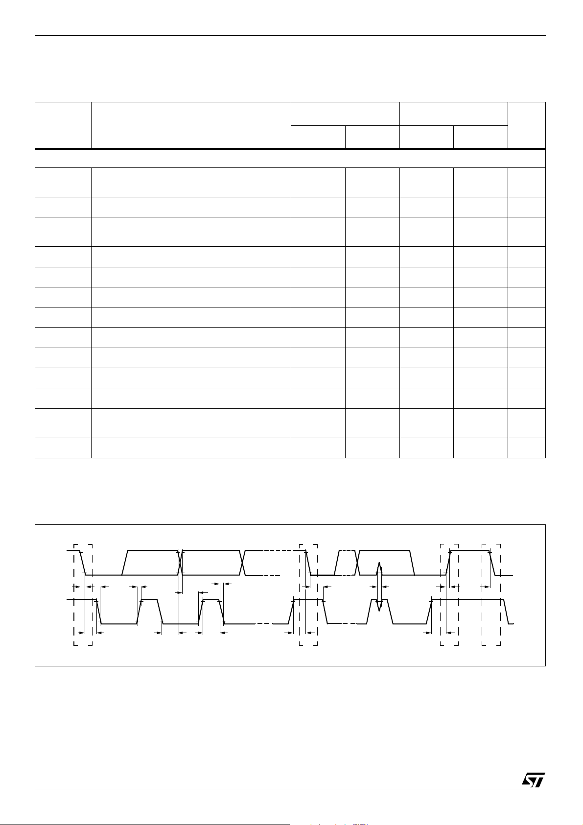
Electrical and Timing Characteristics STV9937
12.4 I²C Bus Characteristics
T able 51: Characteristics of the SDA an SCL bus lines for F/S-mode I²C-bus devices
Standard mode Fast mode
Symbol Parameter
Min. Max. Min. Max.
I²C Interface: SDA and SCL
Unit
t
SP
f
SCL
t
HD;STA
t
LOW
t
HIGH
t
SU; tSTA
t
HD;DAT
t
SU;DAT
t
r
t
f
t
SU; tSTO
t
BUF
C
b
Pulse width of spikes which must be suppressed
by the input filter
n/a n/a 0 50 ns
SCL clock frequency 0 100 0 400 kHz
Hold time (repeated) START Condition. After this
period, the first clock pulse is generated
4.0 0.6 µs
LOW period of the SCL clock 4.7 1.3 µs
HIGH period of the SCL clock 4.0 0.6 µs
Set-up time for a repeated START condition 4.7 0.6 µs
Data hold time 0 3.45 0 0.9 µs
Data set-up time 250 100 ns
Rise time of both SCL and SDA signals 1000
Fall time of both SCL and SDA signals 300
20 + 0.1C
20 + 0.1C
b
b
300 ns
300 ns
Set-up time for STOP condition 4.0 0.6 µs
Bus free time between a STOP and a START
condition
4.7 1.3 µs
Capacitive load for each bus line 400 400 pF
Figure 16: Definition of Timing for F/S-modes
handbook, full page width
SDA
HIGH
t
f
t
SU;STA
SCL
t
HD;DAT
t
SU;DAT
t
t
f
t
LOW
t
HD;STA
S
t
r
46/49
t
HD;STA
Sr
t
SP
t
SU;STO
t
t
r
BUF
P
S
Page 47
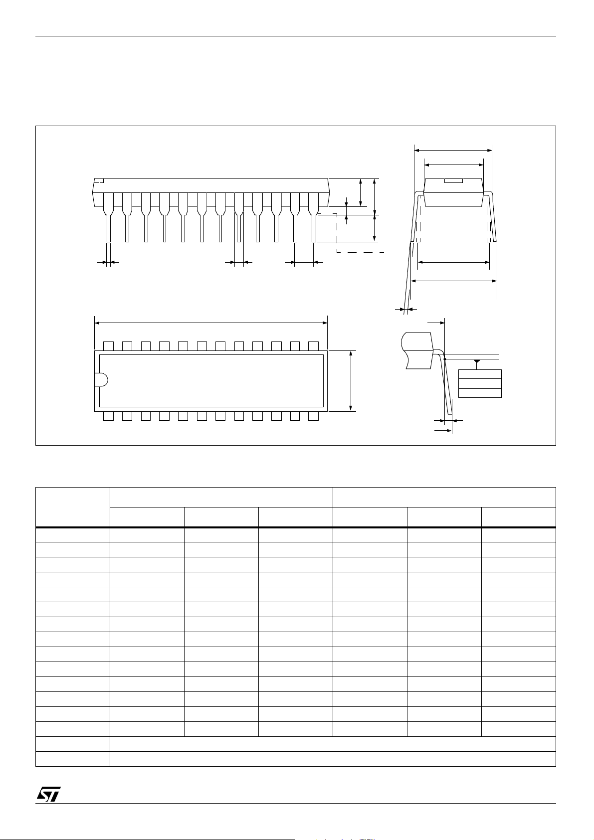
STV9937 Package Mechanical Data
13 Package Mechanical Data
Figure 17: 24-Pin Plastic Dual In-Line Shrink Package
E
E1
A2
A1
A
L
be b2
D
24
1
13
12
Stand -o ff
E1
eA
eB
c
E
0.15 in.
0.38 mm.
Gage Plane
eC
eB
Table 52: PDIP24S Package
mm inches
Dim.
Min. Typ. Max. Min. Typ. Max.
A 5.08 0.200
A1 0.51 0.020
A2 3.05 3.30 4.57 0.120 0.130 0.180
b 0.38 0.46 0.56 0.015 0.018 0.022
b2 0.89 1.02 1.14 0.035 0.040 0.045
c 0.23 0.25 0.38 0.009 0.010 0.015
D 22.35 22.61 22.86 0.880 0.890 0.900
E 7.62 8.64 0.300 0.340
E1 6.10 6.40 6.86 0.240 0.252 0.270
e 1.78 0.070
eA 7.62 0.300
eB 10.92 0.430
eC 0.00 1.52 0.000 0.060
L 2.54 3.30 3.81 0.100 0.130 0.150
Number of Pins
N 24
47/49
Page 48
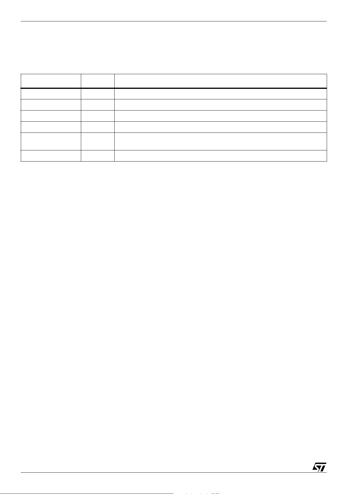
Revision History STV9937
14 Revision History
Table 53: Summary of Modifications
Date Version Description
20 February 2003 0.1 First Draft.
22 May 2003 0.2 General modifications, corrections and updates.
26 June 2003 0.3 Removal of draft status.
08 July 2003 0.4 Update to Figure 3: PictureBooSTTM System Block Diagram on page 6.
24 September 2003 0.5
20 January 2004 0.5 PLL synchronization information added.
Updated Section 10.2:Hardware Hints on page 43 and Figure 15: STV9937 Application
Diagram on page 44.
48/49
Page 49

STV9937
Information furnished is believed to be accura te and reliable. H owever, STMicroelec tronics assu mes no responsibi lity for the
consequences of us e o f s uc h i nfo rma tio n nor for any infringe me nt of p ate nts o r other rights of third part ies w h ich m ay re sul t
from its use. No license is granted by implication or otherwise under any patent or patent rights of STMicroelectronics.
Specifications men tio ned in this publication ar e s ubj ec t to ch ang e w it hou t no tic e. T his pu blication supersedes an d re pla ce s
all information previously supplied. STMicroelectronics products are not authorized for use as critical components in life
support devices or systems without express written approval of STMicroelectronics.
The ST logo is a registered trademark of STMicroelectronics
All other names are the property of their respective owners
© 2004 STMicroelectronics - All rights reserved
STMicroelectronics GROUP OF COMPANIES
Australia - Belgium - Braz il - Canada - Ch ina - Czech Repub lic - Finland - Fran ce - Germany - Hong Kong - India - Israel - Italy
- Japan - Malaysia - Malta - Morocco - Singapore - Spain - Sweden - Switzerland - United Kingdom - United States
www.st.com
49/49
Page 50
WWW.ALLDATASHEET.COM
Copyright © Each Manufacturing Company.
All Datasheets cannot be modified without permission.
This datasheet has been download from :
www.AllDataSheet.com
100% Free DataSheet Search Site.
Free Download.
No Register.
Fast Search System.
www.AllDataSheet.com
 Loading...