

Page 1
STV9380
CLASS-D VERTICAL DEFLECTION AMPLIFIER FOR TV AND
MONITOR APPLICATION
TARGET SPECIFICATION
FEATURES
■ High Efficiency Power Amplifier
■ No Heatsink
■ Split Supply
■ Flyback Generator
■ Output Current up to 2.5 APP
■ Flyback Voltage up to 65V
■ Suitable for DC Coupling Application
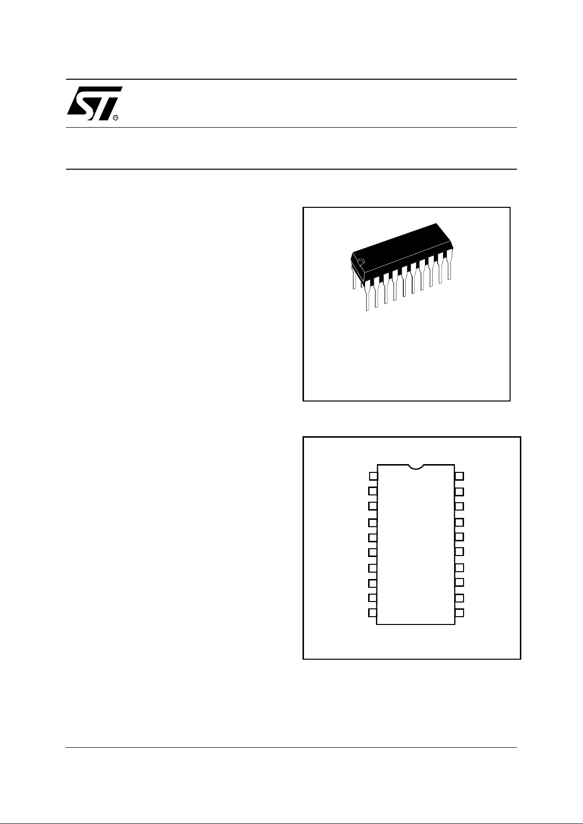
PDIP20 (14+3+3)
ORDER CODE: STV9380
DESCRIPTION
Designed for monitors and TVs, the STV9380 is a
class-D vertical deflection booster assembled in
PDIP20 Package.
It operates with supplies up to +/- 16V , provides
up to 2.5 App output current to drive the yoke. Flyback voltage is close to 65V.
PIN CO NNECTIO N
-V
-V
-V
OUT
CFL Y +
CFLY -
BOOT
VREG
FEEDCAP
FREQ
CC
CC
CC
1
2
3
4
5
6
7
8
9
10
20
19
18
17
16
15
14
13
12
11
-V
CC
-V
CC
-V
CC
-V
CC
+ V
CC
+V
CC
EAout
IN+
IN-
SGND
POW
POW
Version 1.1
May 2000 1/7
This is preliminary information on a new product now in development. Details are subject to change without notice.
1
Page 2
STV9380
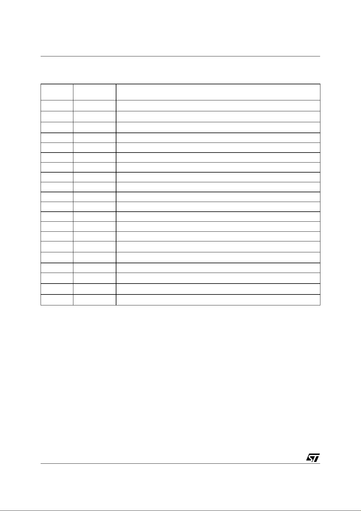
1 - PIN FUNCTIONS
Pin
Number
1-V
2-V
3-V
Name Function
CC
CC
CC
Negative supply
Negative supply
Negative supply
4 OUT PWM Output
5 CFLY+ Flyback capacitor
6 CFLY- Flyback capacitor
7 BOOT Bootstrap capacitor
8 VREG Internal voltage regulator
9 FEEDCAP Feed-back integrated capacitor
10 FREQ Frequency setting resistor
11 SGND Signal Ground
12 IN- Error amplifier inverting input
13 IN+ Error amplifier non-inverting input
14 EA out Error amplifier output
15 +V
16 +V
CC
CC
POW
Positive supply
Positive Power supply
17 -VccPOW Negative Power supply
18 -V
19 -V
20 -V
CC
CC
CC
Negative supply
Negative supply
Negative supply
2/7
2
Page 3
+VCC
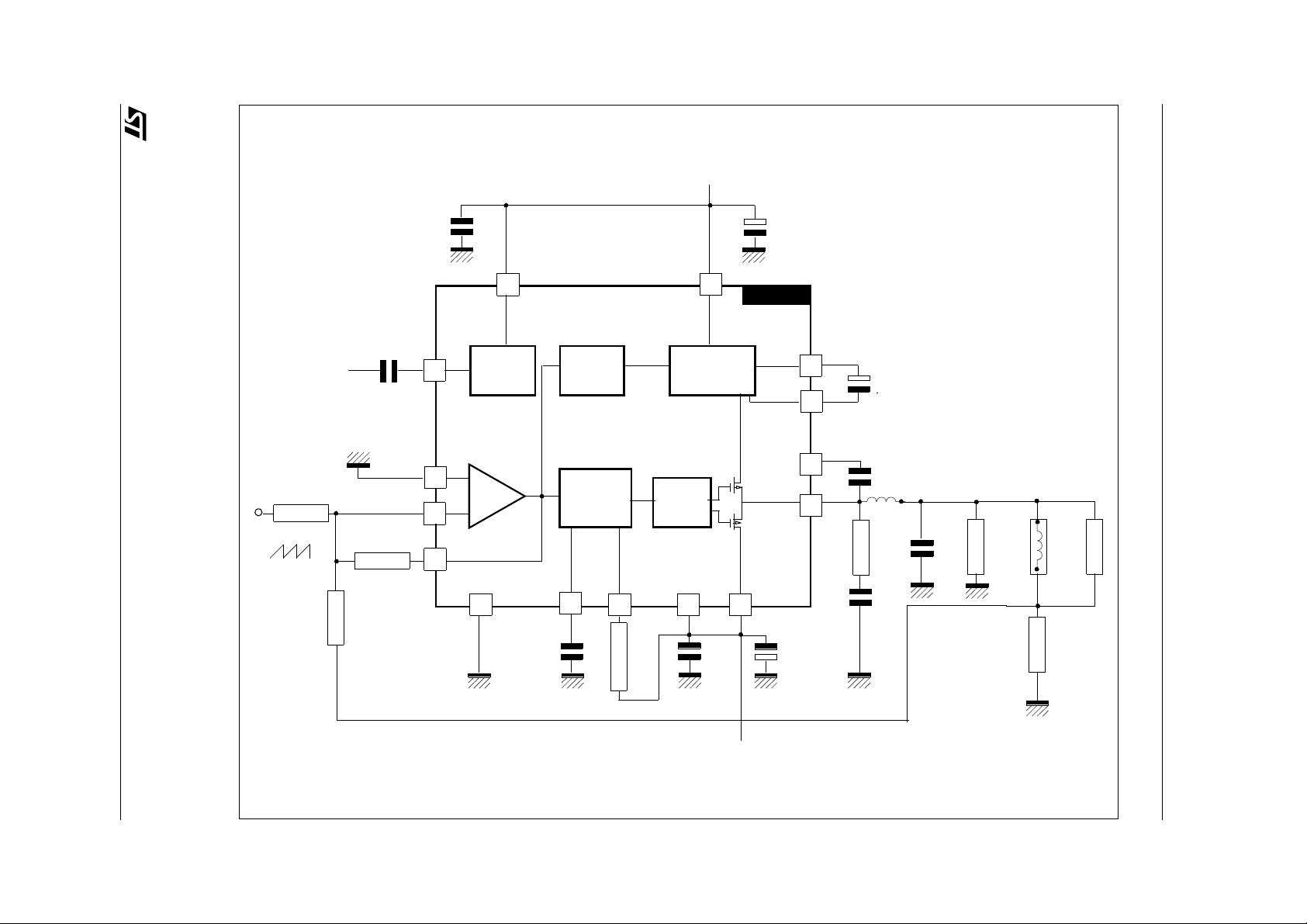
Figure 1. Tes t an d A pplication Ci rc ui t
-VCC
1kΩ
Input signal
1kΩ
100nF
EA out
10kΩ
100nF
VREG
IN+
IN -
8
13
12
14
SGND
15
Vref
+
_
11
FEEDCAP
+VCC
4.7nF
Flyback
detection
Modulator
9
16
Flyback
generator
Output
drive
Pins 1,2,3,18,19,20
10
FREQ
10kΩ
-VCC
100nF 470µF
470µF
+VCC power
STV9 380
TDA9380
17
-VCC power
5
6
7
4
150Ω
CFLY+
CFLY-
BOOT
OUT
CFLYBACK
100µF
Cboot
100nF
1mH
470nF
560pF
150Ω
Deflect.
Yoke
200
0.5Ω
Ω
-VCC
3/7
2
STV9380
Page 4

STV9380
Figure 2. Rth with “on board” Square Heatsink vs. copper area
R
thj-a
(×C/W)
60
COPPER AREA 35
THICKNESS
D97AU675
∝
50
PC BOARD
40
30
0 4 8 12 Area(cm2)
2 - ABSOLUTE MAXIMUM RAT ING
Symbol Parameter Value Unit
VCC DC Supply Voltage ±18 V
, T
T
stg
T
op
VESD
Iout Output current ±1.6 A
Storage and Junction Temperature -40 to +150 °C
j
Operating Temperature Range 0 to +70 °C
ESD Susceptibility - Human Body Model (100 pF discharge through
Ω)
1.5 k
±2 kV
3 - THERMAL DAT A
Symbol Parameter Value Unit
4/7
R
th j-amb
R
th j-pin
Thermal resistance Junction to ambiant 80 °C/W
Thermal Resistance Junction to Pin 12 °C/W
2
Page 5

STV9380
4 - ELECTRIC AL CHARACTERISTICS (refer to Figure 1 on page 3)
Tamb = 25°C unless otherwise specified, Vcc = ±12V
Symbol Parameter Test Conditions Min. Typ. Max. Units
Vcc Supply range ±10 ±16 V
Iout Maximum recommend ed out-
put current
Iq Quiescent supply current Input voltage = 0 TBD TBD mA
, I
I
13
V
SVR Supply voltage rejection TBD TBD dB
Fly
Fly
η
Fsw Switching frequency 120 140 160 kHz
Fsw - op Switching frequency opera -
R
freq
Amplifier Input bias current -0.1 µA
12
Output Offset voltage Input voltage = 0 -50 +50 mV
OS
Flyback detection threshold
thr
positive slope
Flyback detection threshold
thf
negative slope
Efficiency = Po/(Po + Pd)P
tive range
Frequency controller resistor
range
V(14) 1.5 V
V(14) 0.5 V
= 3 W TBD
o
100 200 kHz
71014k
±1.25 A
Ω
5/7
2
Page 6

STV9380
5 - PACKAGE MECHANICAL DAT A
K1
K2 R1
e
b
Z
20
1
B
e3
D D1
11
10
R1
N
a1
I
A
L
N
K
C F
Ee4
TIE BAR CENTER
a2
b1
Dimensions Millimeters Inches
Typ. Min. Max. Typ. Min. Max.
A 3.30 3.18 3.43 0.130 0.125 0.135
a1 0.762 0.508 1.016 0.030 0.020 0.040
a2 1.30 0.051
B 1.27 0.85 1.40 0.050 0.033 0.055
b 0.508 0.45 0.53 0.020 0.018 0.021
b1 0.43 0.38 0.48 0.017 0.015 0.019
C 5.20 6.00 0.205 0.236
D 24.65 24.55 24.77 0.970 0.966 0.975
D1 24.38 24.33 24.45 0.959 0.958 0.962
E 8.80 8.40 9.10 0.346 0.331 0.358
e 2.54 2.29 2.79 0.100 0.090 0.110
e3 22.86 22.60 23.11 0.900 0.890 0.910
e4 7.62 7.36 7.87 0.300 0.290 0.310
F 6.35 6.22 6.47 0.250 0.245 0.255
I 4.06 3.81 4.31 0.160 0.150 0.170
L 3.30 3.00 3.70 0.130 0.118 0.146
N 10d 10d
R1 0.40 0.016
K 2.00 1.90 2.16 0.079 0.075 0.085
K1 2.40 2.30 2.50 0.094 0.090 0.098
K2 0.50 0.45 0.55 0.020 0.018 0.022
Z 1.27 0.050
6/7
3
Page 7

STV9380
Information furnished is believed to be accurate and reliable. However, STMicroelectronics assumes no responsibility for the con sequences of use of suc h informatio n nor for any infringeme nt of patents or other right s of
third parties whi ch ma y res ult fro m its u se. N o licen se is grant ed by implic ation or oth erwi se und er an y patent
or patent rights of STMicroelectronics. Specifications mentioned in this publication are subject to change without notice. This publication supe rsedes and repl aces all informa tion previously s upplied. STMicr oelectronics
products are not auth orized for use as critical componen ts in lif e support devices or syst ems with out the e xpress written approval of STMicroelectronics.
The ST logo is a registered trademark of STMicroelectronics
2000 STMicroelectronics - All Rights Reserved.
Purchase of I
components in an I
2
C Components by STMicroelectronics conveys a license under the Philips I2C Patent. Rights to use these
2
C system is granted provided that the system conforms to the I2C Standard Specification as defined
by Philips.
STMicroelectronics Group of Companies
Australia - Brazil - China - Finland - France - Germany - Hong Kong - India - Italy - Japan - Malaysia - Malta - Morocco -
Singapore - Spain Sweden - Switzerland - United Kingdom - U.S.A.
http://www.st.com
7/7
4
 Loading...