

®
STV8105
256 x 72 x 4-Bit OLED Passive Matrix Controller/Driver
PRODUCT PREVIEW
Description
(Bumped Die)
ORDER CODE:
Main Features
■ Supports Monochrome OLED Passive
Matrices in different formats:
● 256×72 Black & White
● 256×72×2-bits/4 levels of gray
● 256×72×4-bits/16 levels of gray
● 256×36×6-bits/64 levels of gray
● 128×72×6-bits/64 levels of gray
■ On-chip DC/DC Step-up Converter
■ Display Power Supply up to 25V
■ Device Power Supply: 3.0 to 3.6V
■ Low-power Consumption Suitable for
Battery-operated Systems
■ Column Source Current capability: 800µA,
max.
■ Row Sink Current capability: 110mA, max.
STV8105
The STV8105 is a low-power, controller/driver
“combo” IC for OLED displays. The STV8105
supports 256 columns by 72 rows with 16 levels of
gray for monochrome and 2 x 128 columns by 72
rows with 16 lev els of gray f or “two” color displa ys. It
can control a display of 128 columns by 72 rows or
256 columns by 36 rows with 64 levels of gray in
monochrome mode.
The STV8105 provides all necessary functions in a
single chip, including on-chip supply control and
bias current generators, resulting in a minimum of
external components and in very low-power
consumption.
The STV8105 communicates with the system via
fully configurable interfaces (parallel or serial) to
FT
ease interfacing with the host microcontroller. The
STV8105 has a set of command and control
registers that can be addressed by these interfaces.
A
SERIAL PARALLEL
INTERFACE INTERFACE
■ On-chip Oscillator
■ Programmable Gamma Correction
■ Programmable Display Multiplexing
■ Two Brightness Control registers of 128
steps each
■ 32 Step Dimmer Control
■ One Time Programmable (OTP) fuse ROM for
key configuration parameters
■ Dual Scan, Master/Slave Capability
■ Selectable 8-bit Parallel as well as Serial
Peripheral Interfaces
05-Sep-2005 Draft of Rev. 1 STMicroelectronics Confidential 1/96
This is target data for new product. Details are subject to change withou t notic e.
D
R
REGISTERS
ROW
DRIVERS
STATUS
INSTRUCTION DECODER
DISPLAY RAM
256×72 4-bit
SCANNING CONTRO L
COLUMN DRIVERS
CONTROL
REGISTERS
CLOCK
GENERATOR
DC/DC
CONVERTOR
CURRENT
REFERENCES

STV8105
Contents
Chapter 1 General Overview . . . . . . . . . . . . . . . . . . . . . . . . . . . . . . . . . . . . . . . . . . . . . . . . . .5
1.1 Bumped Die Pad Description ...............................................................................................7
1.2 Pad Signal Description ............................................. ..... ...... ..... ................................. ..... .. ..12
1.3 Lead Pad Reference Chart ................................................................................................14
1.4 Mechanical Dimensions .....................................................................................................15
1.5 Functional Description ........................................................................................................16
Chapter 2 Bus Interfaces . . . . . . . . . . . . . . . . . . . . . . . . . . . . . . . . . . . . . . . . . . . . . . . . . . . .17
2.1 Interface Sequence ............................................................................................................17
2.2 Parallel Interface ................................................................................................................18
2.3 Serial Interface ...................................................................................................................20
2.4 Master/Slave Connection ...................................................................................................23
Chapter 3 Display RAM . . . . . . . . . . . . . . . . . . . . . . . . . . . . . . . . . . . . . . . . . . . . . . . . . . . . .25
3.1 16 Level Gray Scale Mode Memory Map ...........................................................................26
FT
3.2 4 Level Gray Scale Mode Memory Map .............................................................................26
3.3 64 Level Gray Scale Mode 1 Memory Map ........................................................................28
3.4 64 Level Gray Scale Mode 2 Memory Map ........................................................................29
3.5 Monochrome Mode Memory Map ......................................................................................30
3.6 Display RAM Loading .........................................................................................................32
Chapter 4 Dot-Matrix Display . . . . . . . . . . . . . . . . . . . . . . . . . . . . . . . . . . . . . . . . . . . . . . . .33
A
R
Chapter 5 Clock Generation . . . . . . . . . . . . . . . . . . . . . . . . . . . . . . . . . . . . . . . . . . . . . . . . .35
Chapter 6 Master/Slave and Primary/Secondary Operation . . . . . . . . . . . . . . . . . . . . . . .37
D
Chapter 7 B rightness Adjustment . . . . . . . . . . . . . . . . . . . . . . . . . . . . . . . . . . . . . . . . . . . .39
Chapter 8 DC/DC Step-up Converter with VF Detection . . . . . . . . . . . . . . . . . . . . . . . . . .41
8.1 General Description ...........................................................................................................41
8.2 Detailed Description ...........................................................................................................42
8.2.1 PWM Mode .............. ..... .................................... ..... ..... .................................... ..... ..... .. ........................................43
8.2.2 PFM Mode ..........................................................................................................................................................44
8.3 Compensation Network ................................................. ...... ..... ..... ................................. ....45
2/96 05-Sep-2005 Draft of Rev. 1 STMicroelectronics Confidential

STV8105
8.4 Soft Start ............................................ ..... ...... ..... ................................. ..... ...... ..... ...............46
8.5 Peak Current Detection ......................................................................................................47
Chapter 9 Column Drivers . . . . . . . . . . . . . . . . . . . . . . . . . . . . . . . . . . . . . . . . . . . . . . . . . . .48
9.1 Color Selection Modes ....................... ..... ...... ................................ ...... ..... ...... ....................48
9.2 Dimmer Control ..................................................................................................................49
9.3 Drive Control ......................................................................................................................50
9.4 Setup Period ......................................................................................................................51
9.5 Drive Period .......................................................................................................................52
9.5.1 16 Level Gray Scale Mode ..................................................................................................................................54
9.5.2 4 Level Gray Scale Mode ....................................................................................................................................55
9.5.3 64 Level Gray Scale Mode ..................................................................................................................................56
9.5.4 Monochrome Mode .............................................................................................................................................58
Chapter 10 Row Driver Control . . . . . . . . . . . . . . . . . . . . . . . . . . . . . . . . . . . . . . . . . . . . . . . .59
10.1 Row Drivers ........................................................................................................................59
10.2 Row Driver Scanning Modes ..............................................................................................59
10.2.1 Single Scanning Mode ........................................................................................................................................59
10.2.2 Dual Scanning Mode ..........................................................................................................................................60
FT
Chapter 11 OTP Memory . . . . . . . . . . . . . . . . . . . . . . . . . . . . . . . . . . . . . . . . . . . . . . . . . . . . .62
11.1 Introduction ........................................................................................................................62
11.2 OTP Memory Programming ...............................................................................................62
11.3 A Short Routine for Programming the OTP ........................................................................63
Chapter 12 STV8105 Configurations . . . . . . . . . . . . . . . . . . . . . . . . . . . . . . . . . . . . . . . . . . .64
12.1 Reset Configuration ...........................................................................................................64
12.2 Sleep Configuration ............................................................................................................64
Chapter 13 Command and Control Registers . . . . . . . . . . . . . . . . . . . . . . . . . . . . . . . . . . . .65
R
A
D
13.1 List of Commands Ordered by Command Code ................................................................66
13.2 Command Details Ordered by Command Code ................................................................68
Chapter 14 Electrical Characteristics . . . . . . . . . . . . . . . . . . . . . . . . . . . . . . . . . . . . . . . . . .91
14.1 Absolute Maximum Ratings ...............................................................................................91
14.2 Thermal Data .....................................................................................................................91
14.3 Recommended Operating Conditio ns ........................... ...... ................................ ...... .........91
05-Sep-2005 Draft of Rev. 1 STMicroelectronics Confidential 3/96

STV8105
14.3.1 DC Characteristics ..............................................................................................................................................91
14.3.2 Timing Generator ................................................................................................................................................92
14.3.3 Row Drivers ........................................................................................................................................................92
14.3.4 Column Drivers ...................................................................................................................................................93
14.3.5 Current Reference and Brightness Adjustment D/A Converter
14.3.6 DC/DC Converter ................................................................................................................................................93
14.3.7 Voltage Generators .............................................................................................................................................94
14.3.8 Reset Input .........................................................................................................................................................94
Chapter 15 Revision History . . . . . . . . . . . . . . . . . . . . . . . . . . . . . . . . . . . . . . . . . . . . . . . . . .96
R
D
FT
A
4/96 05-Sep-2005 Draft of Rev. 1 STMicroelectronics Confidential

STV8105 General Overview
1 General Overview
The STV8105 is a monochrom e , l ow-power co nt ro ll e r/ dri ver combo from STM i cr o ele ct ro ni c s’ family
of controllers for OLED displays. It has been developed to bring a flexible solution to applications
and systems based on OLED passi ve matr ic es.
STV8105 can be used with many different host micro-controllers. It supports a serial bus and a
The
parallel interface covering most of the possible application architectures. This provides easy access
to a set of command and control registers to properly program the
STV8105 includes a dual port Display RAM of 256 x 72 x 4-bits to support the full display
The
capabilities of 256 column and 72 row drivers with several display functions.
The on-chip DC/DC step-up converter generates the necessary supply voltage (18V, typically) for
all row and column drivers from the battery supply.
STV8105.
Processed in BCD technology, the
can source up to 800µA for columns and sink up to 110mA for rows with a display supply of up to
25V. Thanks to the high level of integration, the number of required external components is
drastically reduced.
STV8105 f eatures a low-power digital core and output drivers that
FT
A
R
D
05-Sep-2005 Draft of Rev. 1 STMicroelectronics Confidential 5/96
General Overview STV8105
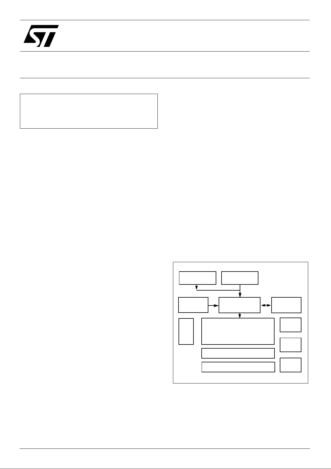
Figure 1: STV8105 Input/Output Diagram
RST
CLKIN
ROSC
COSC
SELCLK
MSEL[1]
MSEL[0]
P/S
DIN[7] (SIN)
DIN[6] (SCLI)
DIN[5:0]
CS1, CS2
SD/C
WR
HSYNCIN
VSYNCIN
VDD
STV8105
A
VPRG
VPP1, VPP2
VROW1, VROW2
VCOL1, VCOL2
COLUMNS
C1…C256
ROWS
R1…R72
DOUT[7] (SOUT)
DOUT[6] (SCLOUT)
DOUT[5:0]
CSOUT1, CSOUT2
SD/COUT
FT
WROUT
HSYNCOUT
VSYNCOUT
RCTRLA
RCTRLB
ROWDATA
SCLKOUT
R
D
TEST[3]
TEST[2:1]
GND
6/96 05-Sep-2005 Draft of Rev. 1 STMicroelectronics Confidential
GNDL
GNDSENSE
VDC
VHSENSE
VDRIVE
ISENSE
VSENSE
VCOMP
VF
TON/F
CMODE
VREF1, VREF2
STV8105 General Overview
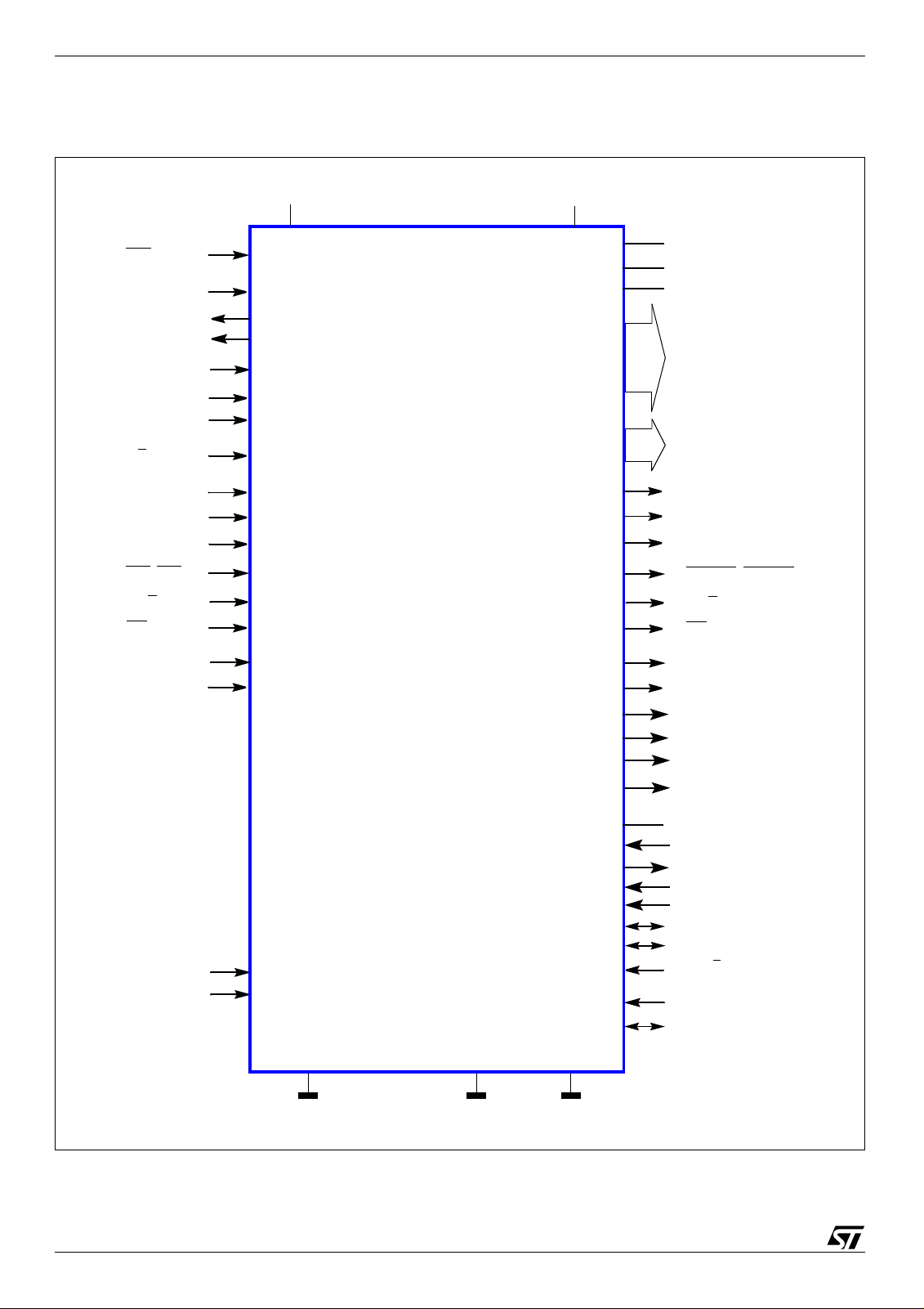
1.1 Bumped Die Pad Description
Figure 2: Die Mechanical Data (Bump-side View)
TOP SIDE
C1
-TBDµm
C256
C255
TBDµm
C2
+TBDµm
R72
LEFT SIDE
R38 R37
R36
-TBDµm
-TBDµm
-TBDµm
-TBDµm
R34
+TBDµm
STV8105
(X=0.0, Y=0.0)
-TBDµm
R2
R4
Figure 3: Alignment Mark Positions (Bump-side View)
Interface
BOTTOM SIDE
-TBDµm
R3
R1
FT
+TBDµm
-TBDµm
+TBDµm
-TBD
R33
+TBDµm
A
-TBDµm
TOP SIDE
+TBDµm
R71
RIGHT SIDE
R35
-TBDµm
+TBDµm
LEFT SIDE
-TBDµm
R
Columns
(X=0.0, Y=0.0)
Rows
Rows
-TBDµm
05-Sep-2005 Draft of Rev. 1 STMicroelectronics Confidential 7/96
D
Interface
BOTTOM SIDE
Rows
+TBDµm
+TBDµm
Rows
RIGHT SIDE
-TBDµm

General Overview STV8105
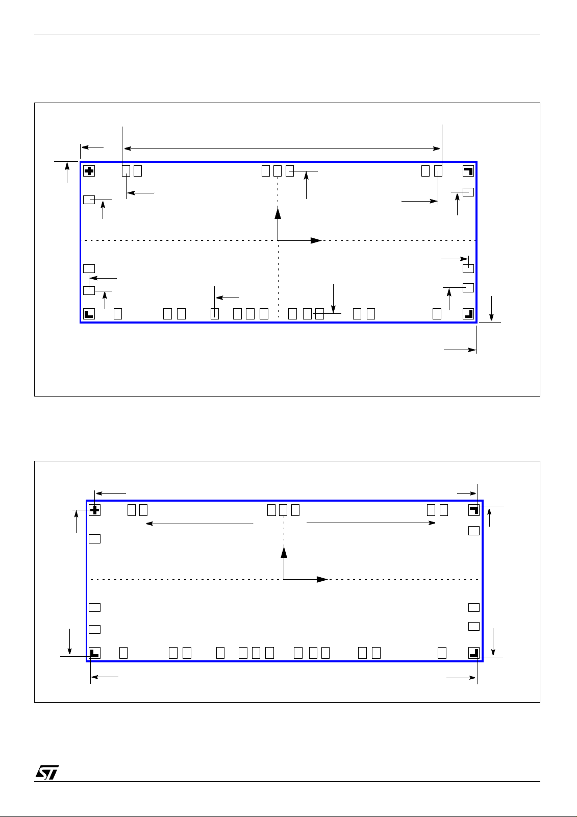
Figure 4: Alignment Mark Mechanical Data
TBDµm
TBDµm
TBDµm
TBDµm
TBDµm
TBDµm
TBDµm
METAL X
TBDµm
COF Alignment Mark
TBDµm
TBDµm
TBDµm
TBDµm
TBDµm
TBDµm
TBDµm
TBDµm
TBDµm
TBDµm
METAL X
TBDµm
TBDµm
TBDµm
TBDµm
Die Positioning Mark
FT
R
D
A
8/96 05-Sep-2005 Draft of Rev. 1 STMicroelectronics Confidential
STV8105 General Overview
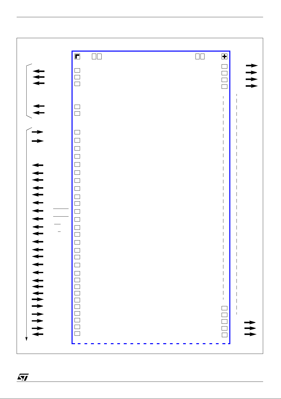
Figure 5: Pad Position (Bump-Side View)
Left
ROW OUTPUTS
INPUTS
- - - -
R34
R32
R30
R4
R2
VROW2
VROW2
DUMMY
DUMMY
ROWDATA
RCTRLB
RCTRLA
SCLKOUT
VSYNCOUT
HSYNCOUT
CSOUT2
CSOUT1
OUT
WR
SD/COUT
DOUT[0]
DOUT[1]
DOUT[2]
DOUT[3]
DOUT[4]
DOUT[5]
DOUT[6]
DOUT[7]
VSENSE
VCOMP
ISENSE
VDC
VDC
VDRIVE
R36
= = =
BOTTOM SIDE
D
R38
= = =
LEFT HALF SIDE
R72
R70
C256
C255
C254
C253
COLUMN OUTPUT SIDE
TOP SIDE
STV8105
FT
A
R
C167
C168
C167
05-Sep-2005 Draft of Rev. 1 STMicroelectronics Confidential 9/96
General Overview STV8105
INPUTS
VDRIVE
VDRIVE
GNDSENSE
GNDSENSE
GNDL
GNDL
GNDL
GNDL
GND
GND
GND
GND
VPRG
VPRG
VPRG
VPRG
VPP2
VPP2
VHSENSE
VHSENSE
VPP1
VPP1
VCOL2
VCOL2
VCOL1
VCOL1
VF
BOTTOM SIDE
STV8105
0,0
+Y
FT
+X
A
C167
C166
C165
COLUMN OUTPUT SIDE
TOP SIDE
VREF2
VREF1
R
VDD
VDD
VDD
VDD
DUMMY
GND
P/S
TON/F
10/96 05-Sep-2005 Draft of Rev. 1 STMicroelectronics Confidential
D
C92
C91
C90
STV8105 General Overview
INPUTS
(95 I/O Pads)
ROW OUTPUTS
- - - -
TON/F
CMODE
SELCLK
MSEL[1]
MSEL[0]
VDD
TEST[3]
TEST[2]
TEST[1]
RST
DIN[7] (SIN)
DIN[6] (SCLI)
DIN[5]
DIN[4]
DIN[3]
DIN[2]
DIN[1]
DIN[0]
SD/C
WR
CS1
CS2
GND
VSYNCIN
HSYNCIN
CLKIN
ROSC
COSC
DUMMY
DUMMY
VROW1
VROW1
R1
R3
R31
R33R33
C90
C89
C88
STV8105
BOTTOM SIDE
COLUMN OUTPUT SIDE
FT
TOP SIDE
A
R
D
C3
= = =
R35
R37
R71
R69
C2
C1
= = =
RIGHT HALF SIDE
05-Sep-2005 Draft of Rev. 1 STMicroelectronics Confidential 11/96
Right
General Overview STV8105
1.2 Pad Signal Description
Table 1: STV8105 Pad Description (Sheet 1 of 2)
Ball Name Input/Output Description
C1-C256 O Column Driver Outputs
R1-R72 O Row Driver Outputs
CLKIN I External RC/Crystal connection or Clock input
Mode Select:
CMODE I
COSC O External RC oscillator, capacitor connection
“H”: Dual color mode
“L”: Single color mode
CS1
CS2
CSOUT1
CSOUT2
DIN[5:0] I
DIN[6] (SCLI) I
DIN[7] (SIN) I
DOUT[5:0] O
DOUT[6] (SCLOUT) O
DOUT[7] (SOUT) O
GND Supply Analog and Digital ground
GNDL Supply Column and Row driver ground
GNDSENSE Supply Ground for DC/DC Converter
I Chip Select 1 Input (Master Device Chip Select)
I Chip Select 2 Input (Slave Device Chip Select)
O Chip Select 1 Output
O Chip Select 2 Output
=”H”: Parallel Data Input
P/S
=”L”: Not used. Fix to “H” or “L”
P/S
=”H”: Parallel Data Input
P/S
P/S
=”L”: Serial Cl ock Input
=”H”: Parallel Data Input
P/S
P/S
=”L”: Serial Data Input
=”H”: Parallel Data Output
P/S
P/S
=”L”: Non Connection
=”H”: Parallel Data Output
P/S
=”L”: Serial Cl ock Output
P/S
=”H”: Parallel Data Output
P/S
P/S
=”L”: Serial Data Output
A
R
FT
HSYNCIN I Horizont al SY NC Input
HSYNCOUT O Horizontal SYNC Output
ISENSE I Over current sense signal for external switching MOS transistor
MSEL[0] I
MSEL[1] I
P/S
RCTRLA O Reserved for Test
RCTRLB O
12/96 05-Sep-2005 Draft of Rev. 1 STMicroelectronics Confidential
I Parallel Interface or Serial Interface Select
D
Master /Slave Select:
“H”: Master
“L”: Slave
Primary /Secondary Select:
“H”: Primary
“L”: Secondary
Pad RCTRLB is pulled “High” if a voltage fault is detected on the output of the
DC/DC converter.
STV8105 General Overview
Table 1: STV8105 Pad Description (Sheet 2 of 2)
Ball Name Input/Output Description
ROSC O External RC oscillator, resistor connection or Crystal connection
ROW DATA O Row Driver Data
RST
SCLKOUT O System Clock Output
SD/C
OUT O SD/C Output
SD/C
SELCLK I
TEST[2:1] I
TEST[3] I Reserved (internal pull-up)
TON/F
VCOL1 Supply Odd column supply
VCOL2 Supply Even column supply
VCOMP I/O Compensation pad for DC/DC converter, constant frequency PWM mode
VDC Supply Supply for gate drive output buffer
I System Reset Input
Display Data or Command:
I
I
SD/C=”H”: Display Data
SD/C
=”L”: Command
“H”: An internal oscillator (if MSEL[0]=”1”)
“L”: External clock used
Test Mode Select:
“H”: Test Mode OFF (internal pull-up)
“L”: Reserved modes
DC/DC Converter Mode Select
“H”: PFM constant t
“L”: PWM constant switching frequency mode
ON
mode
FT
VDD Supply Analog/Digital low-voltage controller supply
VDRIVE O Gate drive for external switchin g MOS transistor
VF I/O
VHSENSE I VH sense input
VPP1 Supply Odd column driver power supply
VPP2 Supply Even column dr iver power supply
VPRG Supply Non-volatile OTP memory program power supply
VREF1 I/O Referen ce Voltag e 1
VREF2 I/O Referen ce Voltag e 2
VROW1 Supply Odd row driver supply
VROW2 Supply Even row driver supply
VSENSE I Feedback signal
VSYNCIN I Vertical SYNC Input
VSYNCOUT O Vertical SYNC Output
WR
OUT O Write Pulse Output
WR
I Display Data and Command Write Pulse
Pad for storing the re sult of VF dete ction, i.e. the average of the voltage on column
outputs C1 and C256 measured during constant current drive
R
D
A
05-Sep-2005 Draft of Rev. 1 STMicroelectronics Confidential 13/96
General Overview STV8105
1.3 Lead Pad Reference Chart
The reference for the following tables is the center of the die (X = 0.0, Y = 0.0)
Table 2: Top Side (from left to right)
Pad Placements (center), µm Pad Dimensions, µm
Lead Pad Name
XYXY
C256 TBD TBD TBD TBD
----- ------- ------- ------- ------C2 TBD TBD
C1 TBD TBD
Table 3: Right Side (from top to bottom)
Pad Placements Pad Dimensions
Lead Pad Name
XYXY
R71 TBD TBD
------- ------- ------- ------- ------R37 TBD TBD
R35 TBD TBD
Table 4: Bottom Side (from right to left)
Pad Placements Pad Dimensions
Lead Pad Name
XYXY
A
FT
TBD TBD
TBD TBD
TBD TBD
TBD TBD
TBD TBD
R33 TBD TBD
------- ------- ------- ------- -------
R1 ------- ------- ------- -------
VROW1 ------- ------- ------- -------
R
TBD TBD
D
------- ------- ------- ------- -------
------- ------- ------- ------- -------
VROW2 ------- ------- ------- -------
R2 ------- ------- ------- -------
------- ------- ------- ------- ------R34 ------- ------- ------- -------
14/96 05-Sep-2005 Draft of Rev. 1 STMicroelectronics Confidential
STV8105 General Overview
Table 5: Left Side (from bottom to top)
Pad Placements Pad Dimensions
Lead Pad Name
XYXY
R36 TBD TBD
R38 TBD TBD
------- ------- ------- ------- ------R72 TBD TBD
1.4 Mechanical Dimensions
Table 6: Mechanical Dimensions
Description Dimension
Die Size (mm) TBD
Pad Pitch (µm) TBD
Pad Size (µm) TBD
Pad Heigh t (µm ) TBD
Wafer Thickness (µm) TBDµm
Bump Size (µm) TBDµm x TBDµm
Bump Characteristics gold, electrolytic
TBD TBD
TBD TBD
TBD TBD
FT
Bump Hardness 30-80Hv
A
R
D
05-Sep-2005 Draft of Rev. 1 STMicroelectronics Confidential 15/96
General Overview STV8105
1.5 Functional Description
The architecture of the STV8105 provides all of the functions required to drive OLED displays. The
block diagram below gives an overview of the different on-chip components, embedded functions
and their links.
Figure 6: STV8105 Block Diagram
SERIAL PARALLEL
INTERFACE INTERFACE
STATUS
REGISTERS
ROW
DRIVERS
INSTRUCTION DECODER
DISPLAY RAM
256×72 4-bit
CONTROL
REGISTERS
CLOCK
GENERATOR
FT
DC/DC
CONVERTER
SCANNING CONTROL
COLUMN DRIVERS
A
CURRENT
REFERENCES
R
The following rules are used in this datasheet to describe bit, bit-fields and registers:
- ROWDRVSEL is the name of a register,
- RDIR.ROWDRVSEL is the RDIR bit of register ROWDRVSEL,
- RMODE.ROWDRVSEL is the RMODE bit-field of register ROWDRVSEL.
Refer to Chapter 13: Command and Control Registers on page 65 for details of the various
registers.
The various functions of the STV8105 are described in the following sections, starting with the bus
interfaces.
16/96 05-Sep-2005 Draft of Rev. 1 STMicroelectronics Confidential
D
STV8105 Bus Interfaces
2 Bus Interfaces
The parallel interface and serial interface are selected using a P/S pad.
The parallel interface is active when P/S
The serial input pads SIN and SCLI are shared with DIN7 and DIN6, respectively.
Buffered versions of the serial signals, for cascading purposes, are output on pads SOUT and
SCLOUT and shared with DOUT7 and DOUT6, respectively.
The parallel interface pads DIN[7:0], CS1
CSOUT1
CS1
CS2
, CSOUT2, and WROUT.
and CSOUT1 are chip select signals for the Primary-Master and Secondary-Master devices.
and CSOUT2 are chip select signals for the Primary-Slave and Secondary-Slave devices.
Figure 7: Buffering of Bus Interface Signals
Internal Circuits
DIN[7] (SIN) DOUT[7] (SOUT)
DIN[6] (SCLI) DOUT[6] (SCLOUT)
DIN[5:0] DOUT[5:0]
=”H”; the serial interface when P/S =”L”.
, CS2 and WR are buff ered and sent out on DOUT[7:0],
FT
CS1
CS2
WR
SD/C
D
2.1 Interface Sequen ce
After Reset or Power ON, an interface is in the state of waiting for a Command Address and Display
RAM Data.
After receiving the Command Address, the interface is in the state of waiting for Command Data.
When Command Data is received while in the receive Command Data state, the interface returns to
the receive Command Address state.
When Display RAM Data is received while in the receive Command Data state, the interface also
returns to the receive Command Address state.
A
R
CSOUT1
CSOUT2
WROUT
SD/COUT
05-Sep-2005 Draft of Rev. 1 STMicroelectronics Confidential 17/96

Bus Interfaces STV8105
When the Serial Interface is selected, the output buffer for the interface signals is cleared when CS1
and CS2
2.2 Parallel Interface
The parallel interface is active when pad P/S is "High".
are both "High".
When writing parallel data, the WR
Data is interpreted as a command if SD/C
"High".
When transmitting a command, the command address is sent first followed by command data.
A command is decided by a 2-byte access: a command code followed by a data byte.
When there is a Display RAM access with SD/C
of a command, the STV8105 enters the state where it is waiting for a Command Address.
CS1, CS2
WR
pad is asserted while CS1 and CS2 are both "Low".
is "Low"; it is interpreted as Display RAM data if SD/C is
set “High” but without respecting the “2-byte nature”
Figure 8: Parallel Interface
FT
SD/C
DIN[7:0]
A
P/S = High Command Data
Command Address
(1 byte)
(1 byte)
Display RAM Data
(1 byte)
Command
(2 bytes)
R
Don’t care
D
18/96 05-Sep-2005 Draft of Rev. 1 STMicroelectronics Confidential

STV8105 Bus Interfaces
Figure 9: 8-bit Parallel Interface Timing Diagram
SD/C
CS1
CS2
WR
WR
DIN[7:0]
VIH
VIL
VIH
VIL
VIH
VIL
VIH
VIL
Taw
Valid
Tcclw
Tcyc
Tds
Tah
Tcchw
Tdh
FT
Valid
SD/COUT
CSOUT1
CSOUT2
WROUT
DOUT[7:0]
VIH
VIL
Tdsdc
VIH
VIL
VIH
VIH
VIL
VIL
VIH
VIL
A
Valid
R
Tdcs
Tdwr
D
Tdd
Valid
05-Sep-2005 Draft of Rev. 1 STMicroelectronics Confidential 19/96
Bus Interfaces STV8105
Table 7: 8-bit Parallel Interface Timing
Symbol Parameter Test Conditions Min. Typ. Max. Units
Tah Address Hold Time WR 10 ns
Taw Address Setup Time WR
Tcyc System Cycle Time CS1
Tcclw Write Pulse Width WR
Tds Data Setup Time DIN[7:0] 60 ns
Tdh Data Hold Time DIN7:0] 10 ns
Tdsdc SD/C Output Delay SD/C
Tdcs CS Output Delay CSOUT1
Tdwr WR Output Delay WR
Tdd DATA Output DOUT[7:0] 30 ns
2.3 Serial Interface
The serial interface is active when P/S is "Low".
, CS2 200 ns
OUT 30 ns
, CSOUT2 30 ns
OUT 30 ns
0ns
60 ns
FT
Serial data is written in using DIN[7] (SIN) and DIN[6] (SCLI) while CS1
Data is interpreted as a command if SD/C
"High".
is "Low"; it is interpreted as Display RAM data if SD/C is
and CS2 are both "Low".
DIN[5:0] are not used; they should be tied either “High” or “Low”.
A
R
D
20/96 05-Sep-2005 Draft of Rev. 1 STMicroelectronics Confidential

STV8105 Bus Interfaces
Figure 10: Serial Interface
CS1, CS2
SD/C
D7 D0 D7 D0 D7 D0
DIN[7](SIN)
DIN[6](SCLI)
DIN[5:0]
Fixed High or Low
P/S = Low
Command Address
(1 byte)
R
D
Command
(2 bytes)
A
Command Data
(1 byte)
FT
Display RAM Data
(1 byte)
Don’t care
05-Sep-2005 Draft of Rev. 1 STMicroelectronics Confidential 21/96

Bus Interfaces STV8105
Figure 11: 4-wire Serial Interface Timing Diagram
Tcss Tcsh
CS1
CS2
SD/C
SCLI
SIN
VIH
VIL
VIH
VIL
VIH
VIL
Tslw
Tsas
TrTf
Tsds
Tsah
Valid
Tscyc
Tshw
Tsdh
Valid
FT
A
Table 8: 4-wire Serial Interface Timing
Symbol Parameter Test Conditions Min. Typ. Max. Units
Tscys Serial Clock Cycle 200 ns
Tshw Pulse Width (High) 90 ns
Tslw Pulse Width (Low) 90 ns
Tsas Address Setup Time 20 ns
Tsah Address Hold Time 20 ns
Tsds Data Setup Time 20 ns
Tsdh Data Hold Time 20 ns
Tcss CS-SCL Time 20 ns
Tcsh CS-SCL Time 20 ns
D
R
22/96 05-Sep-2005 Draft of Rev. 1 STMicroelectronics Confidential
STV8105 Bus Interfaces
2.4 Master/Slave Connection
Figure 12 below shows an example connection between two ICs for Master/Slave mode.
Figure 12: Master/Slave Mode
OLED Panel
From MPU
SCLKOUT
DIN[7:0]
CS1
CS2
WR
SD/C
STV8105 Master STV8105 Slave
DOUT[7:0]
CSOUT2
WROUT
SD/COUT
SCLKOUT
VSYNCOUT, HSYNCOUT
Figure 13: External IC Interface Timing Diagram
FT
VIH
VIL
A
VSYNCIN,
HSYNCIN
VSYNCOUT
HSYNCOUT
RCTRLA
RCTRLB
KDATA
VIH
VIL
R
Tdvso
Tdhso
Tdrca
Tdrcb
Tdrowdata
D
05-Sep-2005 Draft of Rev. 1 STMicroelectronics Confidential 23/96

Bus Interfaces STV8105
Table 9: External IC Interface Timing
Symbol Parameter Test Conditions Min. Typ. Max. Units
Tdvso VSYNCOUT Delay 20 ns
Tdhso HSYNCOUT Delay 20 ns
Tdrca RCTRLA Delay 20 ns
Tdrcb RCTRLB Delay 20 ns
Tdrowdata ROWDATA Delay 20 ns
R
D
FT
A
24/96 05-Sep-2005 Draft of Rev. 1 STMicroelectronics Confidential

STV8105 Display RAM
3 Display RAM
The STV8105 contains a Dual Port, 256 × 72 x 4-bit Display RAM. As shown in Figure 14 below,
Port A is for write only; Port B, read only.
It is possible to access any location thanks to X and Y, programmable pointers with ranges
corresponding to the selected display mode.
The X address is specified with the command RAMXSTART, the Y address with RAMYSTART.
The X and Y addresses can be automatically incremented with bits YINC and XINC of the
GSADDINC command. The GSMODE bit-field of this command is also used to select the display
mode and gray scale. See Section 13.2 for details.
Depending on the selected display mode, one, two or four pictures can be stored in the Display
RAM, and one or two colors can be controlled:
16 level gray scale mode: 256 × 72 × 4 bits - 1 picture - one/two colors
4 level gray scale mode: 256 × 72 × 2 bits - 2 pictures - one/two colors
64 level gray scale mode 1: 128 × 72 × 6 bits - 1 picture - one color
64 level gray scale mode 2: 256 × 36 × 6 bits - 1 picture - one color
Black and White, monochrome mode: 256 × 72 × 1 bit - 4 pictures - one/two colors
Figure 14: Dual Port Display RAM Composition
FT
Display RAM
MPU Write Only Driver Write Only
Port A
Dual-Port RAM
A
256× 72×4-bits
Port B
R
D
05-Sep-2005 Draft of Rev. 1 STMicroelectronics Confidential 25/96
Display RAM STV8105
3.1 16 Level Gray Scale Mode Memory Map
In this mode, the picture has 256 x 72 pixels, and the gray scale of each pixel is defined by the
corresponding 4-bit value stored in Display RAM. This mode is selected using field GSMODE of the
GSADDINC command. Only one picture can be stored in the Display RAM. The range of the
address pointers is 00h to 7Fh for X and 00h to 47h for Y. One byte loaded in Display RAM contains
data for two pixels.See Section 13.2 for details. The “two” color mode can be used; see Section
9.1: Color Selection Modes for details.
Figure 15: 16 Level Gray Scale Mode - Display RAM Organization
X =>
Y =>
Row 1
Row 2
Row 3
Row 71
Row 72
Y 00h, X 00h Y 00h, X 01h Y 00h, X 7Dh Y 00h, X 7Eh Y 00h, X 7Fh
Pxl 0, Pxl 1
Y 01h, X 00h
Col1 Col2 Col254 Col255 Col256
Pxl 0
Pxl 2, Pxl 3
Pxl 1 Pxl 255
Display Screen
Pxl 250, Pxl 251
Pxl 254Pxl 253
Pxl 252, Pxl 253
FT
Display RAM
Y 46h, X 00h
Y 47h, X 00h
A
Pxl 254, Pxl 255
Y 47h, X 7Fh
Col 1* Col 2* Col 3*
Row 1
3.2 4 Level Gray Scale Mode Memory Map
In this mode, the picture has 256 x 72 pixels. The gray scale of each pixel is defined by the
corresponding 2-bit value stored in Display RAM. This mode is selected using field GSMODE of the
GSADDINC command. Two pictures can be stored in the Display RAM. The range of the address
pointers is 00h to 3Fh for X and 00h to 8Fh for Y. One byte loaded in Display RAM contains data for
4 pixels. See Figure 16 for details. The “two” color mode can be used, see Section 9.1: Colo r
Selection Modes for details.
26/96 05-Sep-2005 Draft of Rev. 1 STMicroelectronics Confidential
Pixel 0 Pixel 1 Pixel 2
b3---b0, Byte 00h
Column to Pixel Mapping
b7---b4, Byte 00h
D
R
b3---b0, Byte 01h
Col 255*
Pixel 254
b3---b0, Byte 7Fh
* Default column mapping
Col 256*
Pixel 255
b7---b4, Byte 7Fh
STV8105 Display RAM
Figure 16: 4 Level Gray Scale Mode - Display RAM Organization
Display RAM
X =>
Y =>
Row 1
Row 2
Row 3
Row 71
Row 72
Y 00h, X 00h Y 00h, X 01h Y 00h, X 3Eh Y 00h, X 3Fh
Pxl 0, Pxl 3
Y 01h, X 00h
Y 46h, X 00h
Y 47h, X 00h
Y 48h, X 00h Y 48h, X 01h Y 48h, X 3Eh Y 48h, X 3Fh
Pxl 0, Pxl 3
Y 49h, X 00h
Col1 Col2 Col254 Col255 Col256
Pxl 0
Pxl 4, Pxl 7
Pxl 1 Pxl 255
Display Screen
Picture 1
Pxl 254Pxl 253
Pxl 248, Pxl 251
FT
Pxl 4, Pxl 7
Pxl 248, Pxl 251
A
Pxl 252, Pxl 255
Pxl 252, Pxl 255
Y 47h, X 3Fh
Row 1
Picture 2
R
Y 8Eh, X 00h
Y 8Fh, X 00h
Y 8Fh, X 3Fh
D
Col 1* Col 2* Col 3*
Pixel 0 Pixel 1 Pixel 2
b1---b0, Byte 00h
05-Sep-2005 Draft of Rev. 1 STMicroelectronics Confidential 27/96
b3---b2, Byte 00h
Column to Pixel Mapping
b5---b4, Byte 00h
Col 4*
Pixel 3
b7---b6, Byte 00h
Col 255*
Pixel 254
b5---b4, Byte 7Fh
* Default column mapping
Col 256*
Pixel 255
b7---b6, Byte 7Fh
Display RAM STV8105
3.3 64 Level Gray Scale Mode 1 Memory Map
In this mode, the picture has 128 x 72 pixels. The gray scale of each pixel is defined by the
corresponding 6-bit value stored in Display RAM. This mode is selected using field GSMODE of the
GSADDINC command. Only one picture can be stored in the Display RAM. The range of the
address pointers is 00h to 7Fh for X and 00h to 47h for Y. One byte loaded in the Display RAM
contains data for one pixel.
In this mode, column outputs C
“two” color mode, see Section 9.1: Color Selection Modes for details. For more information on using
this mode, refer to the description of command GSADDINC in Section 13.2.
Figure 17: 64 Level Gray Scale Mode 1 - Display RAM Organization
X =>
Y =>
Row 1
Row 2
Row 3
Row 71
Row 72
and Cn, must be connected together. It is not possible to use the
n+1
Col1 Col2 Col126 Col127 Col128
Pxl 0
Pxl 1 Pxl 127
Display Screen
Pxl 126Pxl 125
FT
Y 00h, X 00h Y 00h, X 01h Y 00h, X 7Dh Y 00h, X 7Eh Y 00h, X 7Fh
Pxl 0
Y 00h, X 00h
Pxl 1
Pxl 125
Pxl 126
Pxl 127
A
Display RAM
Y 46h, X 00h
Y 47h, X 00h
Col 1* Col 2* Col 3*
Row 1
28/96 05-Sep-2005 Draft of Rev. 1 STMicroelectronics Confidential
Pixel 0 Pixel 1 Pixel 2
b5---b0, Byte 00h
Column to Pixel Mapping
D
b5---b0, Byte 01h
128 columns, 72 rows
R
b5---b0, Byte 02h
Y 47h, X 7Fh
Col 127*
Pixel 126
b5---b0, Byte 7Eh
* Default column mapping
Col 128*
Pixel 127
b5---b0, Byte 7Fh

STV8105 Display RAM
3.4 64 Level Gray Scale Mode 2 Memory Map
In this mode, the picture has 256 x 36pixels, the gray scale of each pixel is defined by the
corresponding 6-bit value stored in Display RAM. This mode is selected using field GSMODE of the
GSADDINC command. Only one picture can be stored in the Display RAM. The range of the
address pointers is 00h to FFh for X, 00h to 23h for Y. One byte loaded in the Display RAM contains
data for one pixel.
The “two” color mode cannot be used, see Section 9.1: Color Selection Modes for detail. For more
information on using this mode, refer to the description of command GSADDINC in Section 13.2.
Figure 18: 64 Level Gray Scale Mode 2 - Display RAM Organization
X =>
Y =>
Row 1
Row 2
Row 3
Row 35
Row 36
Col1 Col2 Col254 Col255 Col256
Pxl 0
Pxl 1 Pxl 255
Display Screen
Pxl 254Pxl 253
FT
Y 00h, X 00h Y 00h, X 01h Y 00h, X FDh Y 00h, X FEh Y 00h, X FFh
Pxl 0
Y 00h, X 00h
Pxl 1
Pxl 253
Pxl 254
A
Display RAM
Y 22h, X 00h
R
Y 23h, X 00h
Pxl 255
Y 47h, X FFh
Col 1* Col 2* Col 3*
Row 1
05-Sep-2005 Draft of Rev. 1 STMicroelectronics Confidential 29/96
Pixel 0 Pixel 1 Pixel 2
b5---b0, Byte 00h
Column to Pixel Mapping
256 columns, 36 rows
D
b5---b0, Byte 01h
b5---b0, Byte 02h
Col 255*
Pixel 254
b5---b0, Byte FEh
* Default column mapping
Col 256*
Pixel 255
b5---b0, Byte FFh

Display RAM STV8105
3.5 Monochrome Mode Memory Map
In this mode, the picture has 256 x 72 pixels, and each pixel is black or white depending on the
corresponding 1-bit value stored in Display RAM. This mode is selected using field GSMODE of the
GSADDINC command. Four pictures can be stored in the Display RAM. The “two” color mode can
be used, see Section 9.1: Color S election Modes for details. The range of the address pointers is
00h to 3Fh for X, 00h to 8Fh for Y. One byte loaded in Display RAM contains data for eight pixels.
See Section 13.2.
R
D
FT
A
30/96 05-Sep-2005 Draft of Rev. 1 STMicroelectronics Confidential

STV8105 Display RAM
Figure 19: Monochrome Mode - Display RAM Organization
Display RAM
X =>
Y =>
Row 1
Row 2
Row 3
Row 71
Row 72
Y 00h, X 00h Y 00h, X 01h Y 00h, X 1Eh Y 00h, X 1Fh
Pxl 0, Pxl 7
Y 01h, X 00h
Y 46h, X 00h
Col1 Col2 Col254 Col255 Col256
Pxl 0
Pxl 8, Pxl 15
Pxl 1 Pxl 255
Display Screen
Picture 1
Pxl 254Pxl 253
Pxl 240, Pxl 247
Pxl 248, Pxl 255
FT
Y 47h, X 00h
Y 47h, X 1Fh
Display RAM
Row 1
Column to Pixel Mapping
Y 00h, X 00h Y 00h, X 1Fh
Picture 1
Y 47h, X 00h
Y 48h, X 00h
A
R
Picture 2
Y 8Fh, X 00h Y 8Fh, X 1Fh
Col 1* Col 8*
Pixel 0 Pixel 7
b0, Byte 00h
D
b7, Byte 00h
Y 00h, X 20h Y 00h, X 3Fh
Picture 3
Picture 4
Y 8Fh, X 20h Y 8Fh, X 3Fh
Col 255*
Pixel 254
b6, Byte 1Fh
* Default column mapping
Col 256*
Pixel 255
b7, Byte 1Fh
05-Sep-2005 Draft of Rev. 1 STMicroelectronics Confidential 31/96

Display RAM STV8105
3.6 Display RAM Loading
Four increment modes can be selected using the XINC and YINC bit of the GSADDINC command
as described below:
● If bits YINC and XINC of command GSADDINC are both “Low”, there is no increment of the X
and Y Display RAM addresses.
● If YINC=”High” and XINC=”Low”, then only the Y address of the Display RAM is incremented
as shown is Figure20.
Figure 20: Automatic Increment of Display RAM Y Address
(Y, X): (00h, 00h) (Y, X): (01h, 00h) (Y, X): (FFh, 00h)
● Conversely, if YINC=”Low” and XINC=”High”, then only the X address of the Display RAM is
incremented, Figure 21.
Figure 21: Automatic Increment of Display RAM X Address
(Y, X): (00h, 00h) (Y, X): (00h, 01h) (Y, X): (00h, FFh)
FT
● If YINC and XINC are both ”High”, then both the X and Y addresses of the Display RAM are
incremented. If the X address reaches its limit of FFh, then only Y address will be incremented,
Figure 22.
Figure 22: Automatic Increment Both X and Y Display RAM Addresses
A
R
(Y, X): (00h, 00h) (Y, X): (00h, 01h) (Y, X): (00h, FFh)
(Y, X): (01h, 00h) (Y, X): (01h, 01h) (Y, X): (01h, FFh)
(Y, X): (FFh, 00h) (Y, X): (FFh, 01h) (Y, X): (FFh, FFh)
D
It is the software designer’s responsibility to keep the X and Y address pointers consistent with the
selected display mode by mainly using automatic incrementation to avoid writing data in areas that
are not read.
32/96 05-Sep-2005 Draft of Rev. 1 STMicroelectronics Confidential

STV8105 Dot-Matrix Display
4 Dot-Matrix Display
The STV8105 can display pictures of different resolutions with different shades or levels of gray as
described below:
16 level grayscale mode: 256 × 72 × 4 bits
4 level grayscale mode: 256 × 72 × 2 bits
64 level grayscale mode 1: 128 × 72 × 6 bits
64 levels grayscale mode 2: 256 × 36 × 6 bits
Black and White, monochrome mode: 256 × 72 × 1 bit
The selected picture in Display RAM can be displayed in four different ways thanks to bits VTUR
and HTUR of the command DOTMTRXDIR (command code 11h):
● bit VTUR selects the vertical display direction versus Display RAM contents, Figure 23.
● bit HTUR selects the horizontal display direction versus Display RAM contents, Figure 24. Bit
HTUR applies when writing data into the Display RAM. To get effective horizontal picture
mirroring after changing t he HTUR bit, the pic ture must be re-wr itt en into Display RAM.
The display is turned on when bit DISPON of command DCTRL (10h) is set; bit DISPON is cleared
by default on reset or during power-on reset.
Figure 23: Invert Image - Vertical Direction
Display RAM data
Vertical Direction Invert with VTUR = “0”
R
D
FT
A
Vertical Direction Inver t with VTUR = “1”
05-Sep-2005 Draft of Rev. 1 STMicroelectronics Confidential 33/96

Dot-Matrix Display STV8105
Figure 24: Invert Image - Horizontal Direction
Display RAM data
Horizontal Direction Invert with HTUR = “0” Horizontal Direc tion Invert with HTUR = “1”
The STV8105 can scan a reduced number of rows by programming the SCLN bit-field of command
DOTMTRXSCAN (12h). See Section 13.2 for details regarding commands DCTRL, DOTMTRXDIR
and DOTMTRXSCAN.
R
D
FT
A
34/96 05-Sep-2005 Draft of Rev. 1 STMicroelectronics Confidential

STV8105 Clock Generation
5 Clock Generation
The STV8105 has two on-chip oscillator circuits to generate the internal clock SCLK. One circuit is
dedicated to an external crystal or RC network. It is also possible to source an external clock on pad
CLKIN directly. A second RC oscillator is fully integrated. It does not require any external
components and provides a reference clock of 4.8MHz, typ. The clock source is selected using input
pads SELCLK and MSEL[0].
The internal clock SCLK is buffered and sent to output pad SCLKOUT for slave devices.
The oscillator frequency can be divided by a factor of 2
programming the SDIV bit-field of command SCLKDIV . This sets up a “prescaler” ratio of from 1/1 to
1/128; see Figure 25. For details regarding the SCLKDIV command, see Section 13.2 : Command
Details Ordered by Command Code.
N
, where integer N can range from 0 to 7, by
R
D
FT
A
05-Sep-2005 Draft of Rev. 1 STMicroelectronics Confidential 35/96

Clock Generation STV8105
Figure 25: Clock Generation
CLKIN
COSC
ROSC
SELCLK
MSEL[0]
MSEL[1]
RST
RC oscillator port
Prescaler
(1/1 to 1/128)
Internal RC Osc.
4.8MHz
H
L
H
L
Divide by 2
OSC Stabilizer
No output until amplitude of
oscillator is stabilized.
SCLK
(Internal Display Function)
FT
SCLKOUT
Crystal Usage
D
CLKIN
COSC
(open)
R
ROSC
External Clock Usage
A
CLKIN
COSC
(open)
ROSC
(open)
36/96 05-Sep-2005 Draft of Rev. 1 STMicroelectronics Confidential

STV8105 Master/Slave and Primary/Secondary Operation
6 Master/Slave and Primary/Secondary Operation
Master/Slave operation of two STV8105s allows driving a panel of 512 columns by 72 rows with 16
levels of gray.
Master/Slave plus Primary/Secondary operation of four STV8105s (two along the top of the panel
and two along the bottom, see Figure 26), allows driving 512 columns by 144 rows with 16 levels of
gray.
The STV8105 sets up Primary/Secondary and Master/Slave assignments depending on the state of
input pads MSEL[0] and MSEL[1] as described in Table 10.
Table 10: Master/Slave Operation
MSEL[1] MSEL[0] Test Mode
Secondar y Slave (SS)
Interface signals from the Secondary Master are
LL
received by the Seco ndary Slave.
The Secondary Slave operates synchronously with
Secondar y Master.
Secondary Master (SM)
Interface signals from the Primary Master are received
LH
HL
HH
Primary Master and Secondary Master operate by CS1
Primary Slave and Secondary Slave operate by CS2
D
by the Secondary Master.
A output synchronizing signal is sent to the Secondary
Slave.
Primary Slave (PS)
Interface signals from the Primary Master are received
by the Primar y Slave.
The Primary Slave operates synchronously with
A
Primary Master.
Primary Master (PM)
Interface signals of VSYNCOUT, HSYNCOUT,
OUT, etc. are activated
SD/C
Operation of the Primary Slave and Secondary Master
R
are synchronous with the Primary Master.
Row Driver Control signals RCTRLA/RCTRLB are
activated.
.
FT
.
05-Sep-2005 Draft of Rev. 1 STMicroelectronics Confidential 37/96

Master/Slave and Primary/Secondary Operation STV8105
Figure 26: Master/Slave and Primary/Secondary Operation
512 columns by 72 rows
two color display, 4-bit gray scale
2 column dr ivers
1 row driver
Primary Master/Slave operation
PSPM
STV8105 STV8105
STV8105 STV8105
SM
SS
A
PM
STV8105 STV8105
PS
R
D
512 columns by 144 rows
FT
two color display, 4-bit gray scale
4 column drivers
2 row drivers
Primary Master/Slave and
Secondary Master/Slave operation
38/96 05-Sep-2005 Draft of Rev. 1 STMicroelectronics Confidential

STV8105 Brightness Adjustment
7 Brightness Adjustment
In the STV8105, a brightness (luminance) adjustment changes the current of the column drivers.
The column current is a copy of a reference current which is defined by the ratio of a reference
voltage on pad VREFx to the value of a precision resistor connected between pad VREFx and
ground.
This reference voltage can range from 0.64 to 2.77V. Using a 20K precision resistor, for example,
leads to a reference current of from 32 to 138.5µA. The maximum possible value of this reference
current is 400µA; it can be set with either or
VREF()Rref()⁄ 2.77V()6.925K()⁄=
The reference voltage is generated by an internal 7-bit DAC.
Input data to this DAC can come from an “initial brightness adjustment” register which is loaded by
a BRIGHTx command or from data stored in an on-chip, one-time-programmable, non-volatile
memory (Anti-Fuse OTP Memory). Input data to the DAC is selected with bit RSELx of command
BRIGHTx. By default, the contents of OTP memory are selected as input to the DAC.
However, if the OTP memory is not alre ady programmed, Section 11.2, the DAC will output an
“undetermined” value between the minimum and the maximum possible for VREF. In this case, it is
mandatory to program the DAC using the BRIGHTx command.
.
VREF()Rfef()⁄ 0.64V()0.6K()⁄=
To support displays using “two” color pixels, the STV8105 has two independent brightness
adjustments. Using bits RESLA and RSELB of commands BRIGHTA and BRIGHTB, DAC A and
DAC B are loaded, respectively , with the contents of initial “brightness” registers A and B, or with the
contents of two on-chip non-volatile memories A and B (Anti-Fuse OTP Memory), as shown in
Figure 27.
See Section 13.2 regarding programming “brightness” register A using command BRIGHTA and
“brightness” register B with command BRIGHTB.
As shown in Figure 27, the overall brightness of the display can also be adjusted by a dimmer
control function - with the command DIMMERCTRL. For details regarding this function, refer to
Section 9.2: Dimmer Control.
A
FT
R
D
05-Sep-2005 Draft of Rev. 1 STMicroelectronics Confidential 39/96

Brightness Adjustment STV8105
Figure 27: Control of Initial Brightness Adjustments
CMODE
H
R2
GND
R1
GND
VREF2
VREF1
Iref2
DIMMER
7-bit “Brightness”
DAC B
DIMMER
7
L
Iref1
Iref1 VREF1()R1()⁄=
A
…
C1
C2
7-bit “Brightness”
DAC A
C3
…
C4
FT
7
C255
C256
R
RSELB.BRIGHTB
VPRG
OTP Memory B
Initial Brightness
Adjustment Register B
D
FDCB.BRIGHTB
MPU
40/96 05-Sep-2005 Draft of Rev. 1 STMicroelectronics Confidential
7
OTP Memory A
Initial Brightness
Adjustment Register A
FDCA.BRIGHTA
7
RSELA.BRIGHTA

STV8105 DC/DC Step-up Converter with VF Detection
8 DC/DC Step-up Converter with VF Detection
8.1 General Description
The STV8105 contains a DC/DC converter controller capable of driving an external, 150mA,
switching power MOS transistor with 90% efficiency. With just few external components a step-up
converter can be realized capable of generating up to 25V from a 3 to 12V battery. The switching
frequency can be set in the range of 150 to 300KHz which allows reducing inductor size. Normal
protections such as under voltage lock-out (UVLO), detection against open loop operation and
current overload are also included.
In general, a step-up converter design based on the DC/DC power controller of the STV8105 is
capable of:
● operating from a 3 to 12V battery
● operating from a gate buffer supply (VDC) of 3 to 10V
● producing an adjustable output, V
● sourcing up to 150mA at 18V
● requiring only 10µA in standby
● operating at efficiencies of up to 90%
● operating at switching frequencies of 100, 200, 250 and 300KHz
● protecting against overload, under voltage or open loop conditions
, ranging from 6 to 25V
H
A block diagram of the converter is shown in Figure 28. The output of the converter is V
output can be used to supply the row drivers with VROW1/VROW2 and the column drivers with
VPP1/VPP2 and VCOL1/VCOL2.
The VF detection feature of the DC/DC controller monitors the voltage on column outputs C1 and
C256 during constant current drive and stores an average of the two voltages on a capacitor
connected to pad VF, see C
control block in determining V
to program a 3-bit DAC to output an adjustment to V
where V
can range from 1.5 to 3.5V and one LSB = 286mV.
FOP
in Figure 28. This “detected” voltage is sampled and used by the
VF
. In addition, the VFOP bit-field of command VFDETVAL can be used
H
A
V
H
VF V
R
FT
according to
H
+=
FOP
. This
H
D
05-Sep-2005 Draft of Rev. 1 STMicroelectronics Confidential 41/96

DC/DC Step-up Converter with VF Detectio n S TV8105
Figure 28: DC/DC Step-up Converter - Block Diagram
VDC
VFOP.VFDETVAL
STV8105
_
+
V
DCLKL
VF Detection
VF
internal bandgap
C
VF
R
C
TON/F
VCOMP
reference
VRSL.DCDCCTRL
Control
FOP
BUFFER
VHSENSE
VDC
VDRIVE
VSENSE
ISENSE
FT
GNDSENSE
V
bat
COIL
L
V
H
C
R
SENSE
C
C
Output VH is “clamped” to VH Max. which equals a constant × VBG at the time of VF detection. If VH
Max. is exceeded, then pad RCTRLB is pulled “High” to VDD by the STV8105 indicating a voltage
fault.
D
8.2 Detailed Description
The converter combines the advantages of two control schemes, pulse width modulation (PWM) or
constant switching frequency mode and pulse frequency modulation (PFM) also called constant t
mode, which together provide high efficiency over a wide range of output load current. Selection
between the two modes is done with pad TON/F.
Output V
the VSENSE pad, the other through VHSENSE. The VSENSE-loop is enabled during power-on
where V
VHSENSE-loop is enabled when V
the voltage present on pad VF.
can be adjusted from 6 to 25V by means of two independent closed loops; one is through
H
increases in proportion to the ramp-up characteristics of an internal bandgap source. The
H
A
+
-
R
is determined to have reached steady-state. Here, VH tracks
H
ON
42/96 05-Sep-2005 Draft of Rev. 1 STMicroelectronics Confidential

STV8105 DC/DC Step-up Converter with VF Detection
The DC/DC power controller also includes several protections designed to prevent damage to the
STV8105 or external components. Under voltage lock-out (UVLO) shuts the gate drive buffer down
if VDC becomes too low. The power-off threshold is 2.54V; the power-on threshold, 2.77V. VDC is
internally filtered by the STV8105 so that the power controller does not react to glitches that might
be present on this supply.
Over current protection on pad ISENSE senses the source current of the external switching MOS
transistor and disables the gate drive buffer if this current exceeds 250mV/R
persists for 16 “internal” cycles, the buffer remains off until either VDC is removed or a reset such as
pad RST
Detection of an open-loop condition, either on VSENSE or VHSENSE, causes the STV8105 to also
shut down the gate drive buffer. If an open-loop condition occurs with VHSENSE, then V
value fixed by the external feedback resistor divider.
8.2.1 PWM Mode
When pad TON/F is connected “Low” to GND, the DC/DC converter operates in PWM or constant
switching frequency mode.
The PWM circuit consists of a fixed frequency sawtooth generator, an error amplifier and a PWM
comparator. The frequency of the generator can range from 150 to 300KHz. The default is 150KHz;
the other values are programmed, see Section 13.2, with field FDCDC of command DCDCCTRL.
Referring to Figure 29, the error amplifier is a transconductance operational amplifier (OTA) that
compares an internal bandgap voltage with the voltage on pad VSENSE. The output of the OTA,
pad VCOMP, is available for frequency compensation. The feedback signal on VSENSE is obtained
using an external resister divider across the converter output V
The output of the error amplifier, VCOMP, is compared with the sawtooth wavef o rm. If it is greater,
the external switching MOS transistor is kept ON. If it is less, the MOS transistor is switched OFF.
going “Low” occurs.
.
H
FT
. If this condition
SENSE
rises to a
H
Suppose V
goes “Low” causing the duty cycle to decrease. As a consequence V
feedback is negative and can maintain V
exceeds its steady state value by a small amount, then the output of the error amplifier
H
at its desired value.
H
A
R
D
decreases. Thus the
H
05-Sep-2005 Draft of Rev. 1 STMicroelectronics Confidential 43/96

DC/DC Step-up Converter with VF Detectio n S TV8105
Figure 29: PWM or Constant Switching Frequency Mode
VF
+
_
V
FOP
_
+
VHSENSE
VRSL.DCDCCTRL
DCDCON.DCDCCTRL
PWDWN
Sawtooth
Oscillator
Latch
4-bit counter
VFOP.VFDETVAL
UVLO
+
_
500n s delay
BUFFER
+
_
250mV
VDC
VDRIVE
GNDSENSE
ISENSE
FT
A
8µA
500nA
_
+
1.24V
Bandgap
VSENSE
VCOMP
RST
TON/F
R
8.2.2 PFM Mode
D
When pad TON/F is connected “High” to VDD, the DC/DC converter operates in PFM or constant
t
mode.
ON
Referring to Figure 30, the PFM circuit consists of a t
state by the output of the VSENSE error amplifier. During t
ON. It is switched OFF when a current limit or a t
If output V
“High” and a t
repeatedly, until V
and the clock is disabled. If a current limit is detected during a t
OFF until a another t
obtained.
44/96 05-Sep-2005 Draft of Rev. 1 STMicroelectronics Confidential
becomes less than its steady state value, the output of the error amplifier remains
H
ON/tOFF
period starts. The external MOS transistor is switched ON and OFF,
exceeds the steady state value. Then the output of the error amp goes “Low”,
H
occurs. In this way, the switching frequency is varied until regulation is
ON
ON/tOFF
period occurs.
OFF
oscillator that can be locked in the t
the external MOS transistor is kept
ON
period, the oscillator is locked
ON
GND
OFF

STV8105 DC/DC Step-up Converter with VF Detection
In PFM mode the switching frequency scales roughly in proportion to the load current. Thus, this
mode of operation enables high efficiency with light loads and is ideal to control the converter in
standby mode. The PFM control technique does not need any frequency compensation. It is
inherently stable.
Figure 30: PFM or Constant tON Mode
VF
+
_
V
FOP
_
+
VHSENSE
VRSL.DCDCCTRL
DCDCON.DCDCCTRL
PWDWN
t
t
OFF
Latch
ON
RST
4-bit counter
SRQ
CLK
40µA
R
UVLO
RST
500n s delay
+
_
A
VFOP.VFDETVAL
BUFFER
VDC
VDRIVE
GNDSENSE
ISENSE
FT
250mV
500nA
_
+
1.24V
Bandgap
VSENSE
VCOMP
TON/F
VDD
D
8.3 Compensation Network
The LC output filter in Figure 28 has a two-pole transfer function. So to guarantee stability in PWM
mode, it is necessary to frequency compensate the closed loop response of the converter.
The error amplifier plays a fundamental role in regulating the loop of the converter. This amplifier is
an operational transconductance amplifier (OTA). Since the output of an OTA is high impedance, it
is easy to compensate the converter by connecting an RC network between this node and ground.
Thus the output of the OT A is bought out to a pad, VCOMP, where an external RC can be connected
between it and ground, GND. See R
05-Sep-2005 Draft of Rev. 1 STMicroelectronics Confidential 45/96
and CC in Figure 31 below.
C

DC/DC Step-up Converter with VF Detectio n S TV8105
The external RC introduces a dominant low-frequency pole in the response of the control loop. It
also introduces a zero that can be placed to cancel the pole of the LC output filter.
Operation in PFM mode does not require frequency compensation.
Figure 31: DC/DC Converter - Application Circuit
V
bat
22µF/16V100nF
C
VF
22nF
R
22K
C
47nF
STV8105
VF Detection
VF
internal bandgap
reference, V
VCOMP
C
Ω
C
TON/F
GND
BG
VFOP.VFDETVAL
DCLKL
Control
_
+
V
FOP
A
VHSENSE
VDC
VDRIVE
VSENSE
ISENSE
C6-K1.8L
RB160M
SI2304DS
ESVB2335M
FT
R
SENSE
0.1
GNDSENSE
Ω
V
H
R
A
174K
Ω
R
B
12K
Ω
R
8.4 Soft Start
Soft start is an essential feature for correct power-up of the DC/DC converter without overstressing
the external switching MOS transistor. Soft start operates during start up of the converter when bit
DCDCON of command DCDCCTRL becomes “1”. The soft start function is realized with the same
capacitor, C
calculated by simply taking into account the output sourcing current of the OTA which is 40µA in
PWM mode and 8µA in PFM.
During power-up, the external MOS transistor starts switching with a duty cycle that gradually
increases at the same rate as the voltage on pad VCOMP. In PFM mode, pad VCOMP is used only
for soft start, and the voltage on this pad ramps-up to VDD.
46/96 05-Sep-2005 Draft of Rev. 1 STMicroelectronics Confidential
, that is used for frequency compensation. The soft start ramp-up time can be
C
D

STV8105 DC/DC Step-up Converter with VF Detection
8.5 Peak Current Detection
The drain-source voltage of the external switching MOS transistor is sensed by R
and as soon as a comparator detects that this voltage has exceeded 250mV, the gate drive of the
external MOS transistor is switched OFF.
When the comparator senses an over-current condition, a flip-flop is se t, and the extern al MO S
transistor is switched OFF. The flip-flop remains set while the over-current condition persists. If this
condition persists for 16 continuous “internal” cycles, a master latch turns the DC/DC converter off,
and the conve rter can not be restarted with DCDCON.DCDCCTRL = “1” until after a ne w po w er-up
or hardware reset (RST
An internal low-pass filter in series with pad ISENSE with an inherent delay of 500ns rejects voltage
glitches caused by the external switching MOS transistor during its operation.
Refer to Section 13.2: Command Details Ordered by Command Code for details regarding registers
DCDCCTRL and VFDETVAL which control operation of the DC/DC conve rter.
= “0”) is issued.
SENSE
, Figure 31,
R
D
FT
A
05-Sep-2005 Draft of Rev. 1 STMicroelectronics Confidential 47/96

Column Drivers STV8105
9 Column Drivers
The column drivers of STV8105 are described in Figure 32.
Together, the column driver outputs C1 to C256 can be connected to three different sources or
placed in Hi-Z. The three different source types are: a constant current supplied on pads VPP
constant voltage supplied on pads VCOL
Supply pads VPP1 and VCOL1 are for the odd numbered outputs.
Supply pads VPP2 and VCOL2 are for the even numbered outputs.
The GNDL pad is common to all columns pads.
A dedicated command register (COLCTRL 1Ah) provides 4 control bits to override the column
output signals:
● the CLLM bit, when set to “1” (with CLLZ = “0”), forces all column outputs to VCOL1 and
VCOL2. It overrides all other column commands. The inactive default value is “0”.
● bit CLLZ, when set, forces all column outputs in Hi-Z state and overrides all other commands.
Inactive default value is “0”.
● bit HSLZ, when set, forces output HSYNCOUT to Hi-Z. HSYNCOUT is grounded to pad GNDL
when HSLZ is “0”, the inactive default value.
● bit OFLZ, when set (with CLLM and CLLZ = “0” and after the PWM current sourcing period),
forces all column outputs to Hi-Z, otherwise the outputs are grounded to GNDL when OFLZ is
“0”, the inactive default value.
, or switched to GNDL.
X
X
, a
FT
9.1 Color Selection Modes
The STV8105 can drive dual or “two” color displays: one color appears on the odd columns, the
other on even columns. Supplies VPPx and VCOLx as well as the column current generators can be
set to different levels to fit the driving characteristics of the two colors. Two reference currents are
defined by the selected “brightness” DAC (DAC A or DAC B) and by two precision resistors
connected on pads VREF1 and VREF2. These resistors can have the same or different values. The
dual current reference mode is selected by pulling pad CMODE “High” to VDD.
Note:
● In the dual color mode, the same dimmer control applies to the two colors.
● When using the 64 level gray scale modes (resolutions of 128 × 72 and 256 × 36), the dual
mode cannot be used, supplies VPP1 and VPP2 as well as VCOL1 and VCOL2 must be
connected together, and only DAC A (VREF1) can be used.
● When pad CMODE is pulled “Low” to GND, only one current reference is used. It is defined by
the resistor on pad VREF1 and controlled by DAC A along with the dimmer command. See
Figure 32.
D
A
R
48/96 05-Sep-2005 Draft of Rev. 1 STMicroelectronics Confidential

STV8105 Column Drivers
Figure 32: Column Drivers
CMODE
VREF2
VREF1
GND
VPP1
Iref2
From DAC B
Iref1
From DAC A
VCOL1
GNDL
C1
DIMMER
magnification
DIMMER
magnification
VCOL2VPP2
GNDL
H
L
C2
C255
…
GNDL
FT
A
…
C1 C2 C3 C4 C255 C256
C256
GNDL
Bit HTUR of the command DOTMTRXDIR can be used to reverse the horizontal display direction
versus column pinout. Note that the picture must be reloaded because HTUR can only change the
Display RAM write direction. Refer to Section 13.2 for details.
9.2 Dimmer Control
The brightness of the whole display panel can be changed with the DIMM bit-field of command
DIMMERCTRL. DIMM selects what fraction of I
I
which is given by
COUT
where fract[DIMM] is a fraction depending on the value of field DIMM according to Table 11 bel ow.
For more info on command DIMMERCTRL see Section 13.2.
05-Sep-2005 Draft of Rev. 1 STMicroelectronics Confidential 49/96
R
D
I
COUT
to use in establishing the column output current
ref
Iref fract DIMM[]×=

Column Drivers STV8105
Table 11: Dimmer command
DIMM.DIMMERCTRL fract[DIMM] Ratio of Iref [%]
b4 b3 b2 b1 b0
0 0000 1/16 6.25
0 0001 2/16 12.5
---- ---- ----
0 0011 4/16 25
---- ---- ----
0 0111 8/16 50
---- ---- ----
0 1011 12/16 75
---- ---- ----
0 1111 16/16 100
---- ---- ----
1 0011 20/16 125
---- ---- ----
1 0111 24/16 150
---- ---- ----
1 1011 28/16 175
---- ---- ----
1 1111 32/16 200
Note: Note: A ”Dimmer” adjustment is performed synchronous with VSYNC when bit DISPON of register
DCTRL is “1”. Otherwise, when DISPON.DCTRL is “0”, this adjustment is performed immediately
after the command DIMMERCTRL is issued.
9.3 Drive Control
The STV8105 outputs a constant current on each column pad depending on the “Brightness” and
“Dimmer” levels selected by the user. During the row period, the column current is PWM modulated
according to the gray scale value of each pixel. A row (or scan line) period is divided into an OLED
Setup Period for reset and precharge followed by a Drive Period (constant current gradation
display).
D
R
A
FT
50/96 05-Sep-2005 Draft of Rev. 1 STMicroelectronics Confidential

STV8105 Column Drivers
Figure 33: Setup and Drive Periods
SCLK
HSYNC
Driver
HSYNC Period
GNDL or Hi-Z
9.4 Setup Period
The Setup Period is composed of four programmable sub-periods. Each sub-period is programmed
using a corresponding OELPERIOD1, 2, 3 or 4 (1Bh, 1Ch, 1Dh or 1Eh) command.
The duration of each sub-period can be programmed to be 1 to 64 SCLK clock periods long using
the ExCL bit-field of the corresponding OELPERIODx command, x = 1, 2, 3 or 4. This leads to a
total Setup Period of between 4 and 256 SCLK clock periods as shown in Figure 34.
The column output signal of a column pad can be programmed independently during the four subperiods using the ExST bit-field of the corresponding OELPERIODx command, x = 1, 2, 3 or 4, as
explained below. The selected column driver output can:
1. source a constant current determined by the brightness and dimmer adjustments, Figure 32,
2. be forced to VCOLx,
3. be pulled down to ground GNDL or
4. be placed in a Hi-Z state.
If the pixel value to be displayed is 00h (i.e., black), then independent of whether the selected
column output is programmed to be at VPPx, VCOLx or in Hi-Z during the setup period, the column
output is pulled down to ground GNDL during the whole of the setup period and during the whole of
the drive period as well.
Setup Period
4 to 256 SCLK pulses
R
D
Drive Period
256 SCLK pulses, fixed
FT
A
Note: before the first setup period, 1 SCLK clock period is inserted in a row period sequence. During
this time , th e out put HSY NCOU T can b e pull ed to gr ound G NDL or put in Hi-Z usin g bit OF LZ of the
command COLCTRL (1Ah).
05-Sep-2005 Draft of Rev. 1 STMicroelectronics Confidential 51/96

Column Drivers STV8105
Figure 34: Setup Period Timing
SCLK
HSYNC
Driver
SCLK
HSYNC
Setup Period 1
Setup Period 2
Setup Period 3
Setup Period 4
Setup Period
4 to 256 SCLK pulses
1 to 64 SCLK pulses
OUT (VPP, VCOL, GNDL, Hi-Z)
1 to 64 SCLK pulses
OUT (VPP, VCOL, GNDL, Hi-Z)
Drive Period
256 SCLK pulses, fixed
FT
1 to 64 SCLK pulses
A
OUT (VPP, VCOL, GNDL, Hi-Z)
1 to 64 SCLK pulses
OUT (VPP, VCOL, GNDL, Hi-Z)
R
GNDL or Hi-Z
D
9.5 Drive Period
The active duration of a row period (or scan line period) is named the drive period. The drive period
is 256 SCLK clock periods long.
During the drive period, the column drivers are sourcing constant current defined by the brightness
and dimmer levels selected by the user. The time the column current is sourced is proportional to
the gray scale level of the pixel to be displayed, leading to a PWM modulation. This “sourcing” time
can have 256 different values. After the “sourcing” time elapses, column current is turned off, and
the column pad is switched to ground GNDL until the next setup period.
The STV8105 has a 30 byte look-up table to define the current sourcing duration of the drive
sequence.
52/96 05-Sep-2005 Draft of Rev. 1 STMicroelectronics Confidential

STV8105 Column Drivers
There are15 bytes dedicated to the odd columns and 15 bytes dedicated to the even columns. They
can be loaded thanks to dedicated ODDx and EVENx commands (command codes 2Dh to 1Fh and
3Ch to 2Eh).
Separate ODDx and EVENx lookup tables can be used in case of “two” color modes. For a given
level of gray, the odd and even bytes can be loaded with different values to fit each color brightness
response. The STV8105 uses ODD and EVEN (or ODD only) lookup tables depending on the input
level at pad CMODE. When CMODE is “High”, the ODD lookup table applies to the odd columns,
and the EVEN lookup table applies to the even columns. When CMODE is “Low”, only the ODDx
lookup table is used for both even and odd columns.
For some gray scale modes the lookup tables are not user accessible; see next sections. For details
regarding the ODDx and EVENx commands, refer to Section 13.2: Com ma nd De tai ls Ord ered by
Command Code.
R
D
FT
A
05-Sep-2005 Draft of Rev. 1 STMicroelectronics Confidential 53/96

Column Drivers STV8105
9.5.1 16 Level Gray Scale Mode
In this mode the gray level of each pixel is defined by a 4-bit value stored in the Display RAM,
leading to 16 levels of gray.
Figure 35: 16 Level Gray Scale Mode - Drive Timing
SCLK
HSYNC
Driver
15th gray scale level
14th gray scale level
13th gray scale level
2nd gray scale le vel
Setup Period
4 to 256 SCLK pulses
VCOL 1 to 256 SCLK pulses
VCOL 1 to 256 SCLK pulses
VCOL 1 to 256 SCLK pulses
VCOL 1 to 256 SCLK pulses
R
Drive Period
256 SCLK pulses, fixed
FT
256 SCLK pulses
A
GNDL or Hi-Z
GNDL or Hi-Z
GNDL or Hi-Z
GNDL or Hi-Z
1st gray scale level
0th gray scale level
This mode uses the ODDx and EVENx, or ODDx only, lookup tables to define the column current
sourcing time. There are 15 bytes corresponding to the 15 different, possible values of pixel data in
Display RAM. When the pixel value is 0h, the column current source is off (to GNDL) for the entire
drive period.
Each byte of the lookup table holds a value between 0 to 256 (00h to FFh). This value corresponds
to the number of elementary SCLK clock periods. Each byte of the lookup table is loaded using the
corresponding ODDx or EVENx command.These bytes must be loaded during the power-on/reset
sequence.
54/96 05-Sep-2005 Draft of Rev. 1 STMicroelectronics Confidential
VCOL
GNDL
D
GNDL or Hi-Z

STV8105 Column Drivers
9.5.2 4 Level Gray Scale Mode
In this mode the gray level of each pixel is defined by a 2-bit value stored in the Display RAM,
leading to 4 levels of gray.
Figure 36: 4 Level Gray Scale Mode - Drive Timing
SCLK
HSYNC
Driver
3rd gray scale level
2nd gray scale level
1st gray scale level
0th gray scale level
Setup Period
4 to 256 SCLK pulses
VCOL 1 to 256 SCLK pulses
VCOL 1 to 256 SCLK pulses
R
Drive Period
256 SCLK pulses, fixed
FT
256 SCLK pulses
VCOL 1 to 256 SCLK pulses
A
GNDL
GNDL or Hi-Z
GNDL or Hi-Z
GNDL or Hi-Z
Because only 4 gray levels are used in this mode, only 3 or 6 from among the 15 or 30 lookup tables
are needed:
ODD3, ODD2, ODD1 and EVEN3, EVEN2, EVEN1 when pad CMODE is “High” and ODD3,
ODD2, ODD1 when CMODE is “Low”.
The lookup table bytes must be loaded during the power-on/reset sequence.
05-Sep-2005 Draft of Rev. 1 STMicroelectronics Confidential 55/96
D

Column Drivers STV8105
9.5.3 64 Level Gray Scale Mode
Figure 37: 64 Level Gray Scale Mode - Drive Timing
SCLK
HSYNC
Driver
63rd gray scale level
62nd gray scale level
61st gray scale level
2nd gray scale le vel
Setup Period
4 to 256 SCLK pulses
256 SCLK pulses
VCOL 256 SCLK pulses
VCOL 240 SCLK pulses
VCOL 224 SCLK pulses
VCOL 2 SCLKs GNDL or Hi-Z
R
A
Drive Period
256 SCLK pulses, fixed
FT
GNDL or Hi-Z
GNDL or Hi-Z
1st gray scale level
0th gray scale level
VCOL 1 SCLK
GNDL or Hi-Z
GNDL
D
In this mode the lookup table is not user programmable. It is shown below in T ab le 12 wh ich li sts t he
number of SCLK clock pulses generated for each of the 64 possible values of a 6-bit pixel.
56/96 05-Sep-2005 Draft of Rev. 1 STMicroelectronics Confidential

STV8105 Column Drivers
Table 12: Lookup Table for 64 Level Gray Scale
Mode
Pixel value Lookup byte
binary number of SCLK pulses
11 1111 256
11 1110 240
11 1101 224
11 1100 208
11 1011 200
11 1010 192
11 1001 184
11 1000 176
11 0111 168
11 0110 160
11 0101 152
11 0100 144
10 0011 136
11 0010 128
11 0001 120
11 0000 112
10 1111 108
10 1110 104
10 1101 100
10 1100 96
10 1011 92
10 1010 88
10 1001 84
10 1000 80
10 0111 76
10 0110 72
10 0101 68
10 0100 64
10 0011 60
10 0010 56
D
R
Pixel value Lookup byte
FT
A
binary number of SCLK pulses
01 1110 44
01 1101 42
01 1100 40
01 1011 38
01 1010 36
01 1001 34
01 1000 32
01 0111 30
01 0110 28
01 0101 26
01 0100 24
01 0011 22
01 0010 20
01 0001 18
01 0000 16
00 1111 15
00 1110 14
00 1101 13
00 1100 12
00 1011 11
00 1010 10
00 1001 9
00 1000 8
00 0111 7
00 0110 6
00 0101 5
00 0100 4
00 0011 3
00 0010 2
00 0001 1
00 0000 0
10 0001 52
10 0000 48
01 1111 46
05-Sep-2005 Draft of Rev. 1 STMicroelectronics Confidential 57/96
Note: odd and even columns have the
same value, so there is NO “two” color
mode in the 64 level gray scale modes.

Column Drivers STV8105
9.5.4 Monochrome Mode
In this mode a pixel is ON or OFF depending on the value of the bit in Display RAM. T
sourcing time is 0 when the pixel is OFF. It is equal, in terms of SCLK clock pulses, to the value of
the byte loaded by the corresponding ODD1 or EVEN1 command (CMODE “High”) or by the ODD1
command (CMODE “Low”) when the pixel is ON. The lookup table byte(s) must be loaded during
the power-on/reset sequence.
Figure 38: Monochrome Mode - Drive Timing
SCLK
HSYNC
Setup Period
4 to 256 SCLK pulses
Driver
Drive Period
256 SCLK pulses, fixed
he column current
1st gray scale level
0th gray scale level
R
D
FT
256 SCLK pulses
A
VCOL 1 to 256 SCLK pulses
GNDL
GNDL or Hi-Z
58/96 05-Sep-2005 Draft of Rev. 1 STMicroelectronics Confidential

STV8105 Row Driver Control
10 Row Driver Control
10.1 Row Drivers
The row driver of STV8105 is the 2-transistor structure shown below in Figure 39.
When activated, the row output pad is switched to GNDL. When not active, the row output pad is
pulled-up to the voltage supplied on pads VROW1 and VROW2. The R
GNDL is 10 ohms, max.
Figure 39: Row Drivers
of the MOS transistor to
ON
VROW1
R1
GNDL
Bit VTUR of command DOTMTRXDIR can be used to select the vertical display direction versus
Display RA M contents. Refer to Section 13.2 for details.
The ROWDRVSEL command allows selecting the scanning direction as well as whether single or
dual scanning mode is used.
10.2 Row Driver Scanning Modes
10.2.1 Single Scanning Mode
The single scanning mode is selected when the RMODE bit-field of command ROWDRVSEL is
programmed to “10b”.
VROW2
R2
GNDL
R
GNDL
FT
A
R71
R72
GNDL
In single scanning mode when the RDIR bit of command ROWDRVSEL is “0”, the Row Drivers are
scanned in increasing order from R1 to R72.
When RDIR.ROWDRVSEL is “1”, the rows are scanned in reverse order starting from R72.
D
05-Sep-2005 Draft of Rev. 1 STMicroelectronics Confidential 59/96

Row Driver Control STV8105
Figure 40: Single Scanning
OLED Panel
Line 71
Line 69
Line 3
Line 1
10.2.2 Dual Scanning Mode
The dual scanning mode is selected when the RMODE bit-field of command ROWDRVSEL is
programmed to “11b”.
In dual scanning mode the odd and even row driver scans are simultaneous.
A maximum of 36 lines can be scanned at once, and the 2 row pads can sink with an effective R
of 5 ohms, max.
The scanning direction is changed, again, with bit RDIR of command ROWDRVSEL.
R71
R69
R3
R1
C1
ROWS
R
COLUMNS
STV8109 DIE
Backside View
INTERFACE
IN
INTERFACE
SIGNALS
A
R72
C256
R70
R4
IN
ROWS
R2
Line 72
Line 70
Line 4
Line 2
FT
ON
D
60/96 05-Sep-2005 Draft of Rev. 1 STMicroelectronics Confidential

STV8105 Row Driver Control
Figure 41: Dual Scanning
OLED Panel
Line 36
Line 35
Line 2
Line 1
R71
R69
R3
R1
C1
ROWS
R
COLUMNS
STV8109 DIE
Backside View
INTERFACE
IN
INTERFACE
SIGNALS
A
R72
C256
R70
R4
IN
ROWS
R2
Line 36
Line 35
Line 2
Line 1
FT
D
05-Sep-2005 Draft of Rev. 1 STMicroelectronics Confidential 61/96

OTP Memory STV8105
11 OTP Memory
11.1 Introduction
The OTP (One Time Programmable) Memory consists of a Volatile Memory (VM) made of an array of flipflops and a Non-Volatile Memory (NVM) made of an array of anti-fuses. Every time the STV8105 is poweredon or exits from reset, the OTP is automatically initialized. The NVM is powered on. Calibration and
configuration parameters that are already stored in the NVM are read and latched into VM, then the NVM is
powered off to avoid extra current consumption.
11.2 OT P Memory Programming
In order to store the calibration and configuration parameters permanently, the contents of VM has
to be transferred to the NVM.
Below are details of the commands that allow permanently storing calibration and configuration
data into the NVM.
Comman
d
SHORT
PRGOTP
CKMM
First of all, care has to be taken when the programming voltage is applied to pad VPRG. Before
powering-up VPRG, the internal switch between VPRG and ground (GND) has to be opened by
making sure bit SHORTON of command SHORT is “0”.
The OTP programming procedure is activated with the PRGOTP command. This procedure, which
last about 50ms, autonomously involves blowing the anti-fuses. This procedure also terminates
autonomously.
With the CKMM command it is possible to check if OTP memory has been correctly programmed.
When CKMM is executed, the STV8105 checks the state of an internal “SEAL” bit. If this bit is “1”,
meaning the OTP memory has been correctly programmed, the STV8105 gets reset. If the “SEAL”
bit is not “1”, the CKMM command is ignored.
Function Addr
VPRG internally
shorted to GNDL,
ON/OFF
OTP
Programming
if SEAL bit = “1”,
SW Reset, else
NOP
Command Data
Default
Bit7 Bit6 Bit5 Bit4 Bit3 Bit2 Bit1 Bit0
F30000000
F50000000 1 -
F7------- - -
A
FT
SHORT
ON
01h
R
D
The recommended conditions for “blowing” and achieving a reliable short circuit of the anti-fuses
are:
● Minimum programming current I
● Programming voltage V
● Time to program all cells Twr > 50ms
62/96 05-Sep-2005 Draft of Rev. 1 STMicroelectronics Confidential
= 16V, accepted range 14V < V
PRG
> 250mA
PRG
PRG
< 18V

STV8105 OTP Memory
11.3 A Short Routin e f or Programming the OTP
Below , a short routine that can be used to program and check the OTP memory of the STV8105.
# Power on VDD.
01h # Issue BRIGHTA command, initial brightness “A” adjustment.
00h to 7Fh # Set desired default value for brightness “A”.
02h # Issue BRIGHTB command, initial brightness “B” adjustment.
00h to 7Fh # Set desired default value for brightness “B”.
F3h # Issue SHORT command
00h # with Bit0 of next word, SHORTON, equal to “0”,
# i.e. short is off.
# Now power on VPRG.
F5h # Issue PRGOTP command
01h # with Bit0 of next word equal to “1”.
# Wait 50ms.
# Power down VPRG.
F2h # Issue SOFTRST command, i.e. issue a software reset.
# Power on OLED display supplies VPP1, VPP2, VCOL1,etc.
10h # Issue DCTRL, the dot-matrix display control command,
03h # with all pixels ON.
F7h # Issue the CKMM command to check OTP programming. If
# display goes blank, i.e. OFF, then OTP has been
# programmed correctly.
A
FT
R
D
05-Sep-2005 Draft of Rev. 1 STMicroelectronics Confidential 63/96

STV8105 Configurations STV8105
12 STV8105 Configurations
12.1 Reset Configuration
When pad RST is brought “Low”, the state of the STV8105 is as follows:
● oscillator OFF
● DC/DC Converter OFF
● Column drivers at GNDL
● internal Row d rivers at GNDL
● external IC controls SCLKOUT, VSYNCOUT, HSYNCOUT, RCTRLA, RCTRLB and ROWDATA
are at GND
● all Registers are loaded with their default values (see Table 13)
After RST
considered to be 200ns max after sendin g or issui ng the com ma nd SOF T RST, the state of the
STV8105 becomes:
● oscillator ON
● DC/DC Converter remains OFF but waiting for a command
● Column drivers at GNDL but also waiting for a command
● internal Row drivers at GNDL (waiting for a command)
● External Driver Control: SCLKOUT = SCLK Clock output
● external IC controls VSYNCOUT, HSYNCOUT, RCTRLA, RCTRLB and ROWD ATA are at GND
● all Registers are at their default values (waiting for a command)
SOFTRST is a one byte command and is the only command that can perform a reset of the
STV8105.
12.2 Sleep Configuration
The STV8105 can be placed into a sleep mode with command SLEEP (command code F1h).
Howev er , the STV8105 is f orced out of sleep mode if either command DCDCCTRL (03h) or DCTRL
(10h) is sent, irrespective of the data value that follows their command codes.
When placed IN sleep mode, the state of the STV8105 is as follows:
● oscillator ON
● DC/DC Converter OFF
● Column drivers at GNDL
● internal Row d rivers at GNDL
● all analog circuits powered by VDD are OFF
● all registers as well as the SRAM retain their status
● bus interface active
is released, i.e. brought “High”, or after completion of a software reset, which is
D
FT
A
R
64/96 05-Sep-2005 Draft of Rev. 1 STMicroelectronics Confidential

STV8105 Command and Control Registers
13 Command and Control Registers
The STV8105 has a set of registers to command and control the display system. They are accessed
via the interfaces described in Chapter 2: Bus Interfaces.
The following rules are used in this datasheet to describe bit, bit-fields and registers:
- ROWDRVSEL is the name of a register,
- RDIR.ROWDRVSEL is the RDIR bit of register ROWDRVSEL,
- RMODE.ROWDRVSEL is the RMODE bit-field of register ROWDRVSEL.
Unused bits are read as 0 and must be written as 0.
Dummy or irrelevant bits are noted “D”; their value when read is undefined, they must be written with
0 for future compatibility.
R
D
FT
A
05-Sep-2005 Draft of Rev. 1 STMicroelectronics Confidential 65/96

Command and Control Registers STV8105
13.1 List of Commands Ordered by Command Code
Table 13: Register List Ordered by Increasing Command Code
Register
name
SCLKDIV00h - W00h00000 SDIV SCLK clock divide ratio
BRIGHTA 01h - W 00h
BRIGHTB 02h - W 00h
DCDCCTRL 03h - W 00h ---- FDCDC
RESERVED 04h - - ----------- Do not use, reserved
RESERVED 05h - - ----------- Do not use, reserved
VFDETVAL06h - W00h ----- VFOP
RESERVED 07h - - ----------- Do not use, reserved
---- ---- - - ----------- Do not use, reserved
RESERVED 09h - - ----------- Do not use, reserved
DCTRL10h - W00h-----DINVDALI
DOTMTRXDIR 11h - W 00h - - DUMM - - VTUR HTUR Dot-Matrix Direction select
DOTMTRXSC
AN
RAMXSTART13h - W00h XXXXXXXX
RAMYSTART14h - W00h XXXXXXXX
GSADDINC 15h - W 00h GSMODE - - YINC XINC
DIMMERCTRL 16h - W 0Fh - - - DIMM Dimmer Control
ROWDRVSEL 17h - W 02h - - - RDIR - - RMODE Row Driver Mode Select
RESERVED 18h - - ----------- Do not use, reserved
Comd
code &
access
12h - W 47h - SCLN Dot-Matrix Scanning Line
Reset b7 b6 b5 b4 b3 b2 b1 b0 Comments
RSELA
RSELB
FDCA Initial Brightness adj. A
FDCB Initial Brightness adj. B
DCDC
DC/DC Converter Control
ON
Selection of voltage to add
to VF to produce VH
DISP
Dot-Matrix Display Control
ON
FT
Display RAM X Start
Address
Display RAM Y Start
Address
A
Gray scale and Increme nt
Mode Set
R
RESERVED 19h - - ----------- Do not use, reserved
COLCTRL1Ah - W00h----CLLMCLLZHSLZOFLZColumn Output Control
OELPERIOD1 1Bh - W 0Fh E1 ST E1CL Setup Period 1
OELPERIOD2 1Ch - W 00h E1ST E1CL Setup Period 2
OELPERIOD3 1Dh - W 00h E2ST E2CL Setup Period 3
OELPERIOD4 1Eh - W 00h E3ST E3CL Setup Period 4
ODD15 1Fh - W FFh ODFT Odd 15 Level of Grayscale
ODD14 20h - W AFh ODET Odd 14 Level of Grayscale
ODD13 21h - W 79h ODDT Odd 13 Level of Grayscale
ODD12 22h - W 53h ODCT Odd 12 Level of Grayscale
ODD11 23h - W 39h ODBT Odd 11 Level of Grayscale
ODD10 24h - W 27h ODAT Odd 10 Level of Grayscale
ODD9 25h - W 1Ah OD9T Odd 9 Level of Grayscale
ODD8 26h - W 12h OD8T Odd 8 Level of Grayscale
D
66/96 05-Sep-2005 Draft of Rev. 1 STMicroelectronics Confidential

STV8105 Command and Control Registers
Register
name
ODD7 27h - W 0Ch OD7T Odd 7 Level of Grayscale
ODD6 28h - W 08h OD6T Odd 6 Level of Grayscale
ODD5 29h - W 05h OD5T Odd 5 Level of Grayscale
ODD4 2Ah - W 03h OD4T Odd 4 Level of Grayscale
ODD3 2Bh - W 02h OD3T Odd 3 Level of Grayscale
ODD2 2Ch - W 01h OD2T Odd 2 Level of Grayscal e
ODD1 2Dh - W 00h OD1T Odd 1 Level of Grayscal e
EVEN15 2Eh - W FFh EVFT
EVEN14 2Fh - W AFh EVET
EVEN13 30h - W 79h EVDT
EVEN12 31h - W 53h EVCT
EVEN11 32h - W 39h EVBT
EVEN10 33h - W 27h EVAT
EVEN9 34h - W 1Ah EV9T Even 9 Level of Grayscale
EVEN8 35h - W 12h EV8T Even 8 Leve l of Grayscale
EVEN7 36h - W 0Ch EV7T Even 7 Level of Gr ayscale
EVEN6 37h - W 08h EV6T Even 6 Leve l of Grayscale
EVEN5 38h - W 05h EV5T Even 5 Leve l of Grayscale
EVEN4 39h - W 03h EV4T Even 4 Leve l of Grayscale
EVEN3 3Ah - W 02h EV3T Even 3 Level of Grayscale
EVEN2 3Bh - W 01h EV2T Even 2 Level of Grayscale
EVEN1 3Ch - W 00h EV1T Even 1 Level of Grayscale
RESERVED 3Dh - - ----------- Do not use, reserved
---- ---- - - ----------- Do not use, reserved
RESERVED F0h - - ----------- Do not use, reserved
SLEEPF1h - W00h-------
SOFTRSTF2h - W- - --------Software reset
SHRT F3h - - ----------- OTP programming
RESERVED F4h - - ----------- Do not use, reserved
PRGOTP F5h ----------- OTP programming
RESERVED F6h - - ----------- Do not use, reserved
CKMM F8h ----------- OTP programming
RESERVED F8h - - ----------- Do not use, reserved
RESERVED ---- - - ----------- Do not use, reserved
RESERVED FFh - - ----------- Do not use, reserved
Comd
code &
access
Reset b7 b6 b5 b4 b3 b2 b1 b0 Comments
Even 15 Level of Grayscale
Even 14 Level of Grayscale
Even 13 Level of Grayscale
Even 12 Level of Grayscale
Even 11 Level of Grayscale
Even 10 Level of Grayscale
FT
A
R
SLEEP
Software Sleep IN/OUT
D
Note: For information about commands F3h, F5h and F7h, see Section 11.2: OTP Memory Programming.
05-Sep-2005 Draft of Rev. 1 STMicroelectronics Confidential 67/96

Command and Control Registers STV8105
13.2 Command Details Ordered by Command Code
SCLKDIV - W - SCLK Clock Divider Ratio Select Default value: 00h
Bit 15 Bit 14 Bit 13 Bit 12 Bit 11 Bit 10 Bit 9 Bit 8 Bit 7 Bit 6 Bit 5 Bit 4 Bit 3 Bit 2 Bit 1 Bit 0
Command code Data
00h 00000 SDIV
Bit/Field Name Reset Function
SDIV 000b SCLK clock divider ratio selection
000b = 1/1
001b = 1/2
010b = 1/4
011b = 1/8
100b = 1/16
101b = 1/32
110b = 1/64
111b = 1/128
BRIGHTA
Bit 15 Bit 14 Bit 13 Bit 12 Bit 11 Bit 10 Bit 9 Bit 8 Bit 7 Bit 6 Bit 5 Bit 4 Bit 3 Bit 2 Bit 1 Bit 0
- W - Initial Brightness Adjustment A Default value: 00h
FT
Command code Data
01h
RSELA
FDCA
A
Bit/Field Name Reset Function
FDCA 000 0000b
(00h)
RSELA 0 Selection of input data for A adjustment D/A converter - either OTP Memory A or Register A
BRIGHTB
- W - Initial Brightness Adjustment B Default value: 00h
00h to 7Fh: data to be stored in initial adjustment Register A
0 =anti-fus e OTP Memory A, default
1 = initial adjustment Register A
R
D
Bit 15 Bit 14 Bit 13 Bit 12 Bit 11 Bit 10 Bit 9 Bit 8 Bit 7 Bit 6 Bit 5 Bit 4 Bit 3 Bit 2 Bit 1 Bit 0
Command code Data
02h
RSELB
FDCB
Bit/Field Name Reset Function
FDCB 000 0000b
(00h)
68/96 05-Sep-2005 Draft of Rev. 1 STMicroelectronics Confidential
00h to 7Fh: data to be stored in initial adjustment Register B

STV8105 Command and Control Registers
Bit/Field Name Reset Function
RSELB 0 Selection of input data for B adjustment D/A converter - either OTP Memory B or Register B
0 =anti-fuse OTP Memory B, default
1 = initial adjustment Register B
DCDCCTRL - W - DC/DC Step-up Converter Control Default value: 00h
Bit 15 Bit 14 Bit 13 Bit 12 Bit 11 Bit 10 Bit 9 Bit 8 Bit 7 Bit 6 Bit 5 Bit 4 Bit 3 Bit 2 Bit 1 Bit 0
Command code Data
03h 0 0 0 0 FDCDC VRSL
Bit/Field Name Reset Function
0 DC/DC converter enable
DCDCON
VRSL 0 DC/DC converter control loop tracking selection
FDCDC 00b DC/DC converter operating frequency in PWM mode
VFDETVAL
- W - Selection of Voltage to Add as Adjustment to VH Default value: 00h
0 = disabled (default)
1 = enabled
0 = tracking with VF voltage (default)
1 =tracking with internal bandgap voltage, V
00b = 150KHz (default)
01b = 200KHz
10b = 250KHz
11b = 300KHz
FT
(see Figure 28)
BG
DCDCON
A
Bit 15 Bit 14 Bit 13 Bit 12 Bit 11 Bit 10 Bit 9 Bit 8 Bit 7 Bit 6 Bit 5 Bit 4 Bit 3 Bit 2 Bit 1 Bit 0
Command code Data
06h 00000 VFOP
R
Bit/Field Name Reset Function
VFOP 000b Selection of voltage to add to pad VF to produce VH, the output of DC/DC converter. In
general, VH = VF + V
D
000b = 1.5V
001b = 1.786V
010b = 2.072V
…
110b = 3.214V
111b = 3.5V
Note: 1LSB of field VFOP is approximately 286mV.
05-Sep-2005 Draft of Rev. 1 STMicroelectronics Confidential 69/96
where according to field VFOP, V
FOP
FOP
is:

Command and Control Registers STV8105
DCTRL - W - Dot-Matrix Display Control Default value: 00h
Bit 15 Bit 14 Bit 13 Bit 12 Bit 11 Bit 10 Bit 9 Bit 8 Bit 7 Bit 6 Bit 5 Bit 4 Bit 3 Bit 2 Bit 1 Bit 0
Command code Data
10h 00000DINVDALI
Bit/Field Name Reset Function
DISPON 0 Dot-Matrix display ON/OFF
0 = Display OFF, DC/DC is ON or OFF according to bit DCDCON of register DCDCCTRL, Column
and Row outputs are set to GNDL, Scanning is OFF
1 = Display ON
DALI 0 Dot-Matrix all points or pixel lights ON/OFF (applies with bit DISPON = 1)
0 = all pixel lights OFF (command disabled)
1 = all pixel lights ON
DINV 0 “Reversal” of Do t-M atrix display contents
0 = display contents not “reversed” (command disabled)
1 = display contents “reversed” (reversal operation is applied on data in Display RAM which is in
read mode
DOTMTRXDIR
Bit 15 Bit 14 Bit 13 Bit 12 Bit 11 Bit 10 Bit 9 Bit 8 Bit 7 Bit 6 Bit 5 Bit 4 Bit 3 Bit 2 Bit 1 Bit 0
- W - Dot-Matrix Display Direction Default value: 00h
FT
Command code Data
DISP
ON
11h 0 0 DUMM 0 0 VTUR HTUR
A
Bit/Field Name Reset Function
HTUR 0 Invert image in horizontal direction (inversion is performed at the time of writing data)
0 = image inversion OFF
1 = image inversion ON (see Figure 24)
VTUR 0 Invert image in vertical direct ion
0 = image inversion OFF
1 = image inversion ON (see Figure 23)
DUMM 00b Number of Dummy Lines to precede Scan line
00b = one dummy line to precede scan line
D
01b = two dummy lines to precede scan line
10b = four dummy line s ““
11b = eight dummy lines ““
DOTMTRXSCAN - W - Dot-Matrix Scan Line Select Default value: 47h
Bit 15 Bit 14 Bit 13 Bit 12 Bit 11 Bit 10 Bit 9 Bit 8 Bit 7 Bit 6 Bit 5 Bit 4 Bit 3 Bit 2 Bit 1 Bit 0
Command code Data
12h 0 SCLN
R
70/96 05-Sep-2005 Draft of Rev. 1 STMicroelectronics Confidential

STV8105 Command and Control Registers
Bit/Field Name Reset Function
SCLN 1000111
(47h)
RAMXSTART - W - Display RAM X Starting Address Default value: 00h
Bit 15 Bit 14 Bit 13 Bit 12 Bit 11 Bit 10 Bit 9 Bit 8 Bit 7 Bit 6 Bit 5 Bit 4 Bit 3 Bit 2 Bit 1 Bit 0
Data Reset Function
00h to FFh 00h Display RAM X Address starting value
Scan line select
000 0000b = Line 1 selected as Scan line
000 0001b = Line 2 selected as Scan line
…
100 0110b = Line 71 selected as Scan line
100 0111b = Line 72 selected as Scan line (default)
100 1000b = Do not use
…
111 1110b = Do not use)
111 1111b = Do not use
Command code Data
13h XXXXXXXX
RAMYSTART
Bit 15 Bit 14 Bit 13 Bit 12 Bit 11 Bit 10 Bit 9 Bit 8 Bit 7 Bit 6 Bit 5 Bit 4 Bit 3 Bit 2 Bit 1 Bit 0
Data Reset Function
00h to FFh 00h Display RAM Y Address starting value
GSADDINC
Bit 15 Bit 14 Bit 13 Bit 12 Bit 11 Bit 10 Bit 9 Bit 8 Bit 7 Bit 6 Bit 5 Bit 4 Bit 3 Bit 2 Bit 1 Bit 0
Bit/Field Name Reset Function
- W - Display RAM Y Starting Address Defaul t val ue: 00h
Command code Data
14h XXXXXXXX
A
R
- W - Grayscale Mode Sel. and Disp. RAM Addr. Increment Default value: 00h
D
Command code Data
15h GSMODE 0 0 YINC XINC
FT
XINC 0 Automatic incre m ent of display RAM X address
0 = increment OFF
1 = increment ON
05-Sep-2005 Draft of Rev. 1 STMicroelectronics Confidential 71/96

Command and Control Registers STV8105
Bit/Field Name Reset Function
YINC 0 Automatic incre m ent of display RAM Y address
0 = increment OFF
1 = increment ON
GSMODE 0000b Gray scale mode selection
0000b = 16 gray scale mode
0001b = do not use
0010b = 4 gray scale mode, picture 1
0011b = 4 gray scale mode, picture 2
0100b = 64 gray scale mode 1
0101b = 64 gray scale mode 2
0110b = do not use
0111b = do not use
1000b = monochrome mode, picture 1
1001b = monochrome mode, picture 2
1010b = monochrome mode, picture 3
1011b = monochrome mode, picture 4
1100b = do not use
1101b = do not use
1110b = do not use
1111b = do not use
DIMMERCTRL - W - Dimmer Control Default value: 0Fh
Bit 15 Bit 14 Bit 13 Bit 12 Bit 11 Bit 10 Bit 9 Bit 8 Bit 7 Bit 6 Bit 5 Bit 4 Bit 3 Bit 2 Bit 1 Bit 0
Command code Data
16h 0 0 0 DIMM
Bit/Field Name Reset Function
DIMM 0 1111
(0Fh)
Dimmer select, i.e . fr action of reference current to mirror as output curr en t for each column. In
general, I
of field DIMM as follows:
0 0000b = 1/16
0 0001b = 2/16
0 0010b = 3/16
…
0 1111b = 16/16 (default)
1 0000b = 17/16
…
1 1101b = 30/16
D
1 1110b = 31/16
1 1111b = 32/16
Note: A luminosity control adjustment is performed synchronous with VSYNCIN when bit
DISPON of regist er DCTRL is “1”. Otherwise, i.e. when DISPON is “0”, it is performed
immediately after the command DIMMERCTRL is issued.
= Irefn × fract[DIMM] where n = 1 or 2 and fract[DIMM] is related to the value
COUTn
R
A
FT
72/96 05-Sep-2005 Draft of Rev. 1 STMicroelectronics Confidential

STV8105 Command and Control Registers
ROWDRVSEL - W - Row Driver Mode Selection Default value: 02h
Bit 15 Bit 14 Bit 13 Bit 12 Bit 11 Bit 10 Bit 9 Bit 8 Bit 7 Bit 6 Bit 5 Bit 4 Bit 3 Bit 2 Bit 1 Bit 0
Command code Data
17h 000RDIR00 RMODE
Bit/Field Name Reset Function
RMODE 10b Row driver mode selectio n
00b = do not use, reserved
01b = do not use, reserved
10b = Internal Row driver, Single scanning 72 line mode (default)
11b = Internal Row driver, Dual scanning mode, max. 36 lines, even and odd Row outputs
driven simultaneously
RDIR 0 Row driver scann ing dire ctio n
0 = R1 to R72 (64 lines), default
1 = R72 (64 lines) to R1
COLCTRL
Bit 15 Bit 14 Bit 13 Bit 12 Bit 11 Bit 10 Bit 9 Bit 8 Bit 7 Bit 6 Bit 5 Bit 4 Bit 3 Bit 2 Bit 1 Bit 0
Bit/Field Name Reset Function
OFLZ 0 Column output control: during the drive period, after the PWM current sourcing period, the column
HSLZ
CLLZ
CLLM
- W - Column Output Control Default value: 00h
Command code Data
1Ah CLLM CLLZ HSLZ OFLZ
FT
A
output is forced to:
0 = GNDL
1 = Hi-Z (only if CLLM and CLLZ are “0”)
0 HSYNCOUT output control: during the HSYNC pulse, the HSYNCOUT output is forced to:
0 = GNDL
1 = Hi-Z (only if CLLM and CLLZ are “0”)
0 Column drivers all in Hi-Z.
All column outputs are set to Hi-Z during the setup and drive periods. (Scanning operation is as
usual. All outputs are in Hi-Z.)
0 = OFF (command disabled)
D
1 = All column outputs in Hi-Z (ON)
0 Column outputs all at VCOL.
All column outputs are set to VCOL1 or VCOL2 in all periods. (Scanning operation is as usual. All
outputs are at VCOL1 or VCOL2.) This setup is effective at the time of CLLZ = “0”
0 = OFF (command disabled)
1 = All column outputs at VCOL (ON)
R
05-Sep-2005 Draft of Rev. 1 STMicroelectronics Confidential 73/96

Command and Control Registers STV8105
OELPERIOD1 - W - Setup Period 1 command Default value: 0Fh
Bit 15 Bit 14 Bit 13 Bit 12 Bit 11 Bit 10 Bit 9 Bit 8 Bit 7 Bit 6 Bit 5 Bit 4 Bit 3 Bit 2 Bit 1 Bit 0
Command code Data
1Bh E1ST E1CL
Bit/Field Name Reset Function
E1CL 00 1111b
(0Fh)
E1ST 00b Selection of column output level during Setup Period 1
Setup Period 1, number of clock pulses
The number of c locks in setup period 1 is:
11 1111b = 64 SCLK
11 1110b = 63 SCLK
…
00 1111b = 16SCLK (default)
…
00 0001b = 2 SCLK
00 0000b = 1 SCLK
00 = column outputs at GNDL
01 = outputs placed in Hi-Z
10 = outputs connected to VCOL
11 = column outputs source a constant current determined by the dimmer and brightness
adjustments
This setup is effe ctive at the time CLLM and CLLZ are “0”
When the level of gray scale data is 0, Setup Period 1 is compulsorily set to GNDL even if VPP,
VCOL or Hi-Z was chosen.
FT
A
R
D
74/96 05-Sep-2005 Draft of Rev. 1 STMicroelectronics Confidential

STV8105 Command and Control Registers
OELPERIOD2 - W - Setup Period 2 command Default value: 00h
Bit 15 Bit 14 Bit 13 Bit 12 Bit 11 Bit 10 Bit 9 Bit 8 Bit 7 Bit 6 Bit 5 Bit 4 Bit 3 Bit 2 Bit 1 Bit 0
Command code Data
1Ch E2ST E2CL
Bit/Field Name Reset Function
E2CL 00 0000b Setup Period 2, number of clock pulses
The number of c locks in setup period 2 is:
11 1111b = 64 SCLK
11 1110b = 63 SCLK
…
00 0001b = 2 SCLK
00 0000b = 1 SCLK (default)
E2ST 00b Selection of column output level during Setup Period 2
00 = column outputs at GNDL
01 = outputs placed in Hi-Z
10 = outputs connected to VCOL
11 = column outputs source a constant current determined by the dimmer and brightness
adjustments
This setup is effe ctive at the time CLLM and CLLZ are “0”
When the level of gray scale data is 0, Setup Period 2 is compulsorily set to GNDL even if VPP,
VCOL or Hi-Z was chosen.
FT
R
D
A
05-Sep-2005 Draft of Rev. 1 STMicroelectronics Confidential 75/96

Command and Control Registers STV8105
OELPERIOD3 - W - Setup Period 3 command Default value: 00h
Bit 15 Bit 14 Bit 13 Bit 12 Bit 11 Bit 10 Bit 9 Bit 8 Bit 7 Bit 6 Bit 5 Bit 4 Bit 3 Bit 2 Bit 1 Bit 0
Command code Data
1Dh E3ST E3CL
Bit/Field Name Reset Function
E3CL 00 0000b Setup Period 3, number of clock pulses
The number of c locks in setup period 3 is:
11 1111b = 64 SCLK
11 1110b = 63 SCLK
…
00 0001b = 2 SCLK
00 0000b = 1 SCLK (default)
E3ST 00b Selection of column output level during Setup Period 3
00 = column outputs at GNDL
01 = outputs placed in Hi-Z
10 = outputs connected to VCOL
11 = column outputs source a constant current determined by the dimmer and brightness
adjustments
This setup is effe ctive at the time CLLM and CLLZ are “0”
When the level of gray scale data is 0, Setup Period 3 is compulsorily set to GNDL even if VPP,
VCOL or Hi-Z was chosen.
FT
R
D
A
76/96 05-Sep-2005 Draft of Rev. 1 STMicroelectronics Confidential

STV8105 Command and Control Registers
OELPERIOD4 - W - Setup Period 4 command Default value: 00h
Bit 15 Bit 14 Bit 13 Bit 12 Bit 11 Bit 10 Bit 9 Bit 8 Bit 7 Bit 6 Bit 5 Bit 4 Bit 3 Bit 2 Bit 1 Bit 0
Command code Data
1Eh E4ST E4CL
Bit/Field Name Reset Function
E4CL 00 0000b Setup Period 4, number of clock pulses
The number of c locks in setup period 4 is:
11 1111b = 64 SCLK
11 1110b = 63 SCLK
…
00 0001b = 2 SCLK
00 0000b = 1 SCLK (default)
E4ST 00b Selection of column output level during Setup Period 4
00 = column outputs at GNDL
01 = outputs placed in Hi-Z
10 = outputs connected to VCOL
11 = column outputs source a constant current determined by the dimmer and brightness
adjustments
This setup is effe ctive at the time CLLM and CLLZ are “0”
When the level of gray scale data is 0, Setup Period 4 is compulsorily set to GNDL even if VPP,
VCOL or Hi-Z was chosen.
FT
ODD15
Bit 15 Bit 14 Bit 13 Bit 12 Bit 11 Bit 10 Bit 9 Bit 8 Bit 7 Bit 6 Bit 5 Bit 4 Bit 3 Bit 2 Bit 1 Bit 0
Bit/Field Name Reset Function
ODFT FFh
- W - Loading byte 15 of the ODD gray scale lookup table Default value: FFh
Command code Data
1Fh ODFT
Number of SCLK clock periods for the odd 15
D
0000 0000b = 1 SCLK
…
0111 1111b = 128 SCLK
…
1111 1111b = 256 SCLK
Note: this command is not to be sent in the following display modes: 4 level gray scale, 64 level
gray scale and monochrome.
R
A
th
level of gray
05-Sep-2005 Draft of Rev. 1 STMicroelectronics Confidential 77/96

Command and Control Registers STV8105
ODD14 - W - Loading byte 14 of the ODD gray scale lookup table Default value: AFh
Bit 15 Bit 14 Bit 13 Bit 12 Bit 11 Bit 10 Bit 9 Bit 8 Bit 7 Bit 6 Bit 5 Bit 4 Bit 3 Bit 2 Bit 1 Bit 0
Command code Data
20h ODET
Bit/Field Name Reset Function
ODET AFh
ODD13
Bit 15 Bit 14 Bit 13 Bit 12 Bit 11 Bit 10 Bit 9 Bit 8 Bit 7 Bit 6 Bit 5 Bit 4 Bit 3 Bit 2 Bit 1 Bit 0
Bit/Field Name Reset Function
ODDT 79h
- W - Loading byte 13 of the ODD gray level lookup table Default value: 79h
Number of SCLK clock periods for the odd 14
0000 0000b = 1 SCLK
…
0111 1111b = 128 SCLK
…
1111 1111b = 256 SCLK
Note: this command is not to be sent in the following display modes: 4 level gray scale, 64 level
gray scale and monochrome.
Command code Data
21h ODDT
Number of SCLK clock periods for the odd 13
0000 0000b = 1 SCLK
…
0111 1111b = 128 SCLK
…
1111 1111b = 256 SCLK
Note: this command is not to be sent in the following display modes: 4 level gray scale, 64 level
gray scale and monochrome.
R
A
th
level of gray
FT
th
level of gray
ODD12
Bit 15 Bit 14 Bit 13 Bit 12 Bit 11 Bit 10 Bit 9 Bit 8 Bit 7 Bit 6 Bit 5 Bit 4 Bit 3 Bit 2 Bit 1 Bit 0
78/96 05-Sep-2005 Draft of Rev. 1 STMicroelectronics Confidential
- W - Loading byte 12 of the ODD gray scale lookup table Default value: 53h
D
Command code Data
22h ODCT

STV8105 Command and Control Registers
Bit/Field Name Reset Function
ODCT 53h
ODD11 - W - Loading byte 11 of the ODD gray scale lookup table Default value: 39h
Bit 15 Bit 14 Bit 13 Bit 12 Bit 11 Bit 10 Bit 9 Bit 8 Bit 7 Bit 6 Bit 5 Bit 4 Bit 3 Bit 2 Bit 1 Bit 0
Bit/Field Name Reset Function
ODBT 39h
Number of SCLK clock periods for the odd 12
0000 0000b = 1 SCLK
…
0111 1111b = 128 SCLK
…
1111 1111b = 256 SCLK
Note: this command is not to be sent in the following display modes: 4 level gray scale, 64 level
gray scale and monochrome.
Command code Data
23h ODBT
Number of SCLK clock periods for the odd 11
0000 0000b = 1 SCLK
…
0111 1111b = 128 SCLK
…
1111 1111b = 256 SCLK
Note: this command is not to be sent in the following display modes: 4 level gray scale, 64 level
gray scale and monochrome.
th
level of gray
th
level of gray
FT
A
ODD10
Bit 15 Bit 14 Bit 13 Bit 12 Bit 11 Bit 10 Bit 9 Bit 8 Bit 7 Bit 6 Bit 5 Bit 4 Bit 3 Bit 2 Bit 1 Bit 0
- W - Loading byte 10 of the ODD gray scale lookup table Default value: 27h
Command code Data
R
24h ODAT
Bit/Field Name Reset Function
ODAT 27h
D
Number of SCLK clock periods for the odd 10
0000 0000b = 1 SCLK
…
0111 1111b = 128 SCLK
…
1111 1111b = 256 SCLK
Note: this command is not to be sent in the following display modes: 4 level gray scale, 64 level
gray scale and monochrome.
th
level of gray
05-Sep-2005 Draft of Rev. 1 STMicroelectronics Confidential 79/96

Command and Control Registers STV8105
ODD9 - W - Loading byte 9 of the ODD gray scale lookup table Default value: 1Ah
Bit 15 Bit 14 Bit 13 Bit 12 Bit 11 Bit 10 Bit 9 Bit 8 Bit 7 Bit 6 Bit 5 Bit 4 Bit 3 Bit 2 Bit 1 Bit 0
Command code Data
25h OD9T
Bit/Field Name Reset Function
OD9T 1Ah
ODD8
Bit 15 Bit 14 Bit 13 Bit 12 Bit 11 Bit 10 Bit 9 Bit 8 Bit 7 Bit 6 Bit 5 Bit 4 Bit 3 Bit 2 Bit 1 Bit 0
Bit/Field Name Reset Function
OD8T 12h
- W - Loading byte 8 of the ODD gray scale lookup table Default value: 12h
Number of SCLK clock periods for the odd 9
0000 0000b = 1 SCLK
…
0111 1111b = 128 SCLK
…
1111 1111b = 256 SCLK
Note: this command is not to be sent in the following display modes: 4 level gray scale, 64 level
gray scale and monochrome.
Command code Data
26h OD8T
Number of SCLK clock periods for the odd 8
0000 0000b = 1 SCLK
…
0111 1111b = 128 SCLK
…
1111 1111b = 256 SCLK
Note: this command is not to be sent in the following display modes: 4 level gray scale, 64 level
gray scale and monochrome.
R
A
th
level of gray
FT
th
level of gray
ODD7
Bit 15 Bit 14 Bit 13 Bit 12 Bit 11 Bit 10 Bit 9 Bit 8 Bit 7 Bit 6 Bit 5 Bit 4 Bit 3 Bit 2 Bit 1 Bit 0
80/96 05-Sep-2005 Draft of Rev. 1 STMicroelectronics Confidential
- W - Loading byte 7 of the ODD gray scale lookup table Default value: 0Ch
D
Command code Data
27h OD7T

STV8105 Command and Control Registers
Bit/Field Name Reset Function
OD7T 0Ch
ODD6 - W - Loading byte 6 of the ODD gray level lookup table Default value: 08h
Bit 15 Bit 14 Bit 13 Bit 12 Bit 11 Bit 10 Bit 9 Bit 8 Bit 7 Bit 6 Bit 5 Bit 4 Bit 3 Bit 2 Bit 1 Bit 0
Bit/Field Name Reset Function
OD6T 08h
Number of SCLK clock periods for the odd 7
0000 0000b = 1 SCLK
…
0111 1111b = 128 SCLK
…
1111 1111b = 256 SCLK
Note: this command is not to be sent in the following display modes: 4 level gray scale, 64 level
gray scale and monochrome.
Command code Data
28h OD6T
Number of SCLK clock periods for the odd 6
0000 0000b = 1 SCLK
…
0111 1111b = 128 SCLK
…
1111 1111b = 256 SCLK
Note: this command is not to be sent in the following display modes: 4 level gray scale, 64 level
gray scale and monochrome.
th
level of gray
th
level of gray
FT
A
ODD5
Bit 15 Bit 14 Bit 13 Bit 12 Bit 11 Bit 10 Bit 9 Bit 8 Bit 7 Bit 6 Bit 5 Bit 4 Bit 3 Bit 2 Bit 1 Bit 0
- W - Loading byte 5 of the ODD gray level lookup table D efaul t val ue: 05h
Command code Data
R
29h OD5T
Bit/Field Name Reset Function
OD5T 05h
D
Number of SCLK clock periods for the odd5
0000 0000b = 1 SCLK
…
0111 1111b = 128 SCLK
…
1111 1111b = 256 SCLK
Note: this command is not to be sent in the following display modes: 4 level gray scale, 64 level
gray scale and monochrome.
th
level of gray
05-Sep-2005 Draft of Rev. 1 STMicroelectronics Confidential 81/96

Command and Control Registers STV8105
ODD4 - W - Loading byte 4 of the ODD gray level lookup table Default value: 03h
Bit 15 Bit 14 Bit 13 Bit 12 Bit 11 Bit 10 Bit 9 Bit 8 Bit 7 Bit 6 Bit 5 Bit 4 Bit 3 Bit 2 Bit 1 Bit 0
Command code Data
2Ah OD4T
Bit/Field Name Reset Function
OD4T 03h
ODD3
Bit 15 Bit 14 Bit 13 Bit 12 Bit 11 Bit 10 Bit 9 Bit 8 Bit 7 Bit 6 Bit 5 Bit 4 Bit 3 Bit 2 Bit 1 Bit 0
Bit/Field Name Reset Function
OD3T 02h
- W - Loading byte 3 of the ODD gray level lookup table D efaul t val ue: 02h
Number of SCLK clock periods for the odd 4
0000 0000b = 1 SCLK
…
0111 1111b = 128 SCLK
…
1111 1111b = 256 SCLK
Note: this command is not to be sent in the following display modes: 4 level gray scale, 64 level
gray scale and monochrome.
Command code Data
2Bh OD3T
Number of SCLK clock periods for the odd 3
0000 0000b = 1 SCLK
…
0111 1111b = 128 SCLK
…
1111 1111b = 256 SCLK
Note: this command is not to be sent in the following display modes: 64 level gray scale and
monochrome.
R
A
th
level of gray
FT
rd
level of gray
ODD2
Bit 15 Bit 14 Bit 13 Bit 12 Bit 11 Bit 10 Bit 9 Bit 8 Bit 7 Bit 6 Bit 5 Bit 4 Bit 3 Bit 2 Bit 1 Bit 0
82/96 05-Sep-2005 Draft of Rev. 1 STMicroelectronics Confidential
- W - Loading byte 2 of the ODD gray level lookup table D efaul t val ue: 01h
D
Command code Data
2Ch OD2T

STV8105 Command and Control Registers
Bit/Field Name Reset Function
OD2T 01h
ODD1 - W - Loading byte 1 of the ODD gray level lookup table Default value: 00h
Bit 15 Bit 14 Bit 13 Bit 12 Bit 11 Bit 10 Bit 9 Bit 8 Bit 7 Bit 6 Bit 5 Bit 4 Bit 3 Bit 2 Bit 1 Bit 0
Bit/Field Name Reset Function
OD1T 00h
Number of SCLK clock periods for the odd 2
0000 0000b = 1 SCLK
…
0111 1111b = 128 SCLK
…
1111 1111b = 256 SCLK
Note: this command is not to be sent in the following display modes: 64 level gray scale and
monochrome.
Command code Data
2Dh OD1T
Number of SCLK clock periods for the odd 1
0000 0000b = 1 SCLK
…
0111 1111b = 128 SCLK
…
1111 1111b = 256 SCLK
Note: this command is not to be sent while display is in 64 level gray scale mode
nd
level of gray
st
level of gray
FT
EVEN15
Bit 15 Bit 14 Bit 13 Bit 12 Bit 11 Bit 10 Bit 9 Bit 8 Bit 7 Bit 6 Bit 5 Bit 4 Bit 3 Bit 2 Bit 1 Bit 0
Bit/Field Name Reset Function
EVFT FFh
- W - Loading byte 15 of the EVEN gray level lookup table Default value: FFh
Command code Data
2Eh EVFT
Number of SCLK clock periods for the even 15
D
0000 0000b = 1 SCLK
…
0111 1111b = 128 SCLK
…
1111 1111b = 256 SCLK
Note: this command is not to be sent in the following display modes: 4 level gray scale, 64 level
gray scale and monochrome.
R
A
th
level of gray
05-Sep-2005 Draft of Rev. 1 STMicroelectronics Confidential 83/96

Command and Control Registers STV8105
EVEN14 - W - Loading byte 14 of the EVEN gray level lookup table Default value: AFh
Bit 15 Bit 14 Bit 13 Bit 12 Bit 11 Bit 10 Bit 9 Bit 8 Bit 7 Bit 6 Bit 5 Bit 4 Bit 3 Bit 2 Bit 1 Bit 0
Command code Data
2Fh EVET
Bit/Field Name Reset Function
EVET AFh
EVEN13
Bit 15 Bit 14 Bit 13 Bit 12 Bit 11 Bit 10 Bit 9 Bit 8 Bit 7 Bit 6 Bit 5 Bit 4 Bit 3 Bit 2 Bit 1 Bit 0
Bit/Field Name Reset Function
EVDT 79h
- W - Loading byte 13 of the EVEN gray level lookup table Default value: 79h
Number of SCLK clock periods for the even 14
0000 0000b = 1 SCLK
…
0111 1111b = 128 SCLK
…
1111 1111b = 256 SCLK
Note: this command is not to be sent in the following display modes: 4 level gray scale, 64 level
gray scale and monochrome.
Command code Data
30h EVDT
Number of SCLK clock periods for the even 13
0000 0000b = 1 SCLK
…
0111 1111b = 128 SCLK
…
1111 1111b = 256 SCLK
Note: this command is not to be sent in the following display modes: 4 level gray scale, 64 level
gray scale and monochrome.
R
A
th
level of gray
FT
th
level of gray
EVEN12
Bit 15 Bit 14 Bit 13 Bit 12 Bit 11 Bit 10 Bit 9 Bit 8 Bit 7 Bit 6 Bit 5 Bit 4 Bit 3 Bit 2 Bit 1 Bit 0
84/96 05-Sep-2005 Draft of Rev. 1 STMicroelectronics Confidential
- W - Loading byte 12 of the EVEN gray level lookup table Default value: 53h
D
Command code Data
31h EVCT

STV8105 Command and Control Registers
Bit/Field Name Reset Function
EVCT 53h
EVEN11 - W - Loading byte 11 of the EVEN gray level lookup table Default value: 39h
Bit 15 Bit 14 Bit 13 Bit 12 Bit 11 Bit 10 Bit 9 Bit 8 Bit 7 Bit 6 Bit 5 Bit 4 Bit 3 Bit 2 Bit 1 Bit 0
Bit/Field Name Reset Function
EVBT 39h
Number of SCLK clock periods for the even 12
0000 0000b = 1 SCLK
…
0111 1111b = 128 SCLK
…
1111 1111b = 256 SCLK
Note: this command is not to be sent in the following display modes: 4 level gray scale, 64 level
gray scale and monochrome.
Command code Data
32h EVBT
Number of SCLK clock periods for the even 11
0000 0000b = 1 SCLK
…
0111 1111b = 128 SCLK
…
1111 1111b = 256 SCLK
Note: this command is not to be sent in the following display modes: 4 level gray scale, 64 level
gray scale and monochrome.
th
level of gray
th
level of gray
FT
A
EVEN10
Bit 15 Bit 14 Bit 13 Bit 12 Bit 11 Bit 10 Bit 9 Bit 8 Bit 7 Bit 6 Bit 5 Bit 4 Bit 3 Bit 2 Bit 1 Bit 0
- W - Loading byte 10 of the EVEN gray level lookup table Default value: 27h
Command code Data
R
33h EVAT
Bit/Field Name Reset Function
EVAT 27h
D
Number of SCLK clock periods for the even 10
0000 0000b = 1 SCLK
…
0111 1111b = 128 SCLK
…
1111 1111b = 256 SCLK
Note: this command is not to be sent in the following display modes: 4 level gray scale, 64 level
gray scale and monochrome.
th
level of gray
05-Sep-2005 Draft of Rev. 1 STMicroelectronics Confidential 85/96

Command and Control Registers STV8105
EVEN9 - W - Loading byte 9 of the EVEN gray level lookup table Default value: 1Ah
Bit 15 Bit 14 Bit 13 Bit 12 Bit 11 Bit 10 Bit 9 Bit 8 Bit 7 Bit 6 Bit 5 Bit 4 Bit 3 Bit 2 Bit 1 Bit 0
Command code Data
34h EV9T
Bit/Field Name Reset Function
EV9T 1Ah
EVEN8
Bit 15 Bit 14 Bit 13 Bit 12 Bit 11 Bit 10 Bit 9 Bit 8 Bit 7 Bit 6 Bit 5 Bit 4 Bit 3 Bit 2 Bit 1 Bit 0
Bit/Field Name Reset Function
EV8T 12h
- W - Loading byte 8 of the EVEN gray level lookup table Default value: 12h
Number of SCLK clock periods for the even 9
0000 0000b = 1 SCLK
…
0111 1111b = 128 SCLK
…
1111 1111b = 256 SCLK
Note: this command is not to be sent in the following display modes: 4 level gray scale, 64 level
gray scale and monochrome.
Command code Data
35h EV8T
Number of SCLK clock periods for the even 8
0000 0000b = 1 SCLK
…
0111 1111b = 128 SCLK
…
1111 1111b = 256 SCLK
Note: this command is not to be sent in the following display modes: 4 level gray scale, 64 level
gray scale and monochrome.
R
A
th
level of gray
FT
th
level of gray
EVEN7
Bit 15 Bit 14 Bit 13 Bit 12 Bit 11 Bit 10 Bit 9 Bit 8 Bit 7 Bit 6 Bit 5 Bit 4 Bit 3 Bit 2 Bit 1 Bit 0
86/96 05-Sep-2005 Draft of Rev. 1 STMicroelectronics Confidential
- W - Loading byte 7 of the EVEN gray level lookup table Default value: 0Ch
D
Command code Data
36h EV7T

STV8105 Command and Control Registers
Bit/Field Name Reset Function
EV7T 0Ch
EVEN6 - W - Loading byte 6 of the EVEN gray level lookup table Default value: 08h
Bit 15 Bit 14 Bit 13 Bit 12 Bit 11 Bit 10 Bit 9 Bit 8 Bit 7 Bit 6 Bit 5 Bit 4 Bit 3 Bit 2 Bit 1 Bit 0
Bit/Field Name Reset Function
EV6T 08h
Number of SCLK clock periods for the even 7
0000 0000b = 1 SCLK
…
0111 1111b = 128 SCLK
…
1111 1111b = 256 SCLK
Note: this command is not to be sent in the following display modes: 4 level gray scale, 64 level
gray scale and monochrome.
Command code Data
37h EV6T
Number of SCLK clock periods for the even 6
0000 0000b = 1 SCLK
…
0111 1111b = 128 SCLK
…
1111 1111b = 256 SCLK
Note: this command is not to be sent in the following display modes: 4 level gray scale, 64 level
gray scale and monochrome.
th
level of gray
th
level of gray
FT
A
EVEN5
Bit 15 Bit 14 Bit 13 Bit 12 Bit 11 Bit 10 Bit 9 Bit 8 Bit 7 Bit 6 Bit 5 Bit 4 Bit 3 Bit 2 Bit 1 Bit 0
- W - Loading byte 5 of the EVEN gray level lookup table Default value: 05h
Command code Data
R
38h EV5T
Bit/Field Name Reset Function
EV5T 05h
D
Number of SCLK clock periods for the even 5
0000 0000b = 1 SCLK
…
0111 1111b = 128 SCLK
…
1111 1111b = 256 SCLK
Note: this command is not to be sent in the following display modes: 4 level gray scale, 64 level
gray scale and monochrome.
th
level of gray
05-Sep-2005 Draft of Rev. 1 STMicroelectronics Confidential 87/96

Command and Control Registers STV8105
EVEN4 - W - Loading byte 4 of the EVEN gray level lookup table Default value: 03h
Bit 15 Bit 14 Bit 13 Bit 12 Bit 11 Bit 10 Bit 9 Bit 8 Bit 7 Bit 6 Bit 5 Bit 4 Bit 3 Bit 2 Bit 1 Bit 0
Command code Data
39h EV4T
Bit/Field Name Reset Function
EV4T 03h
EVEN3
Bit 15 Bit 14 Bit 13 Bit 12 Bit 11 Bit 10 Bit 9 Bit 8 Bit 7 Bit 6 Bit 5 Bit 4 Bit 3 Bit 2 Bit 1 Bit 0
Bit/Field Name Reset Function
EV3T 02h
- W - Loading byte 3 of the EVEN gray scale lookup table Default value: 02h
Number of SCLK clock periods for the even 4
0000 0000b = 1 SCLK
…
0111 1111b = 128 SCLK
…
1111 1111b = 256 SCLK
Note: this command is not to be sent in the following display modes: 4 level gray scale, 64 level
gray scale and monochrome.
Command code Data
3Ah EV3T
Number of SCLK clock periods for the even 3
0000 0000b = 1 SCLK
…
0111 1111b = 128 SCLK
…
1111 1111b = 256 SCLK
Note: this command is not to be sent in the following display modes: 64 level gray scale and
monochrome.
R
A
th
level of gray
FT
rd
level of gray
EVEN2
Bit 15 Bit 14 Bit 13 Bit 12 Bit 11 Bit 10 Bit 9 Bit 8 Bit 7 Bit 6 Bit 5 Bit 4 Bit 3 Bit 2 Bit 1 Bit 0
88/96 05-Sep-2005 Draft of Rev. 1 STMicroelectronics Confidential
- W - Loading byte 2 of the EVEN gray level lookup table Default value: 01h
D
Command code Data
3Bh EV2T

STV8105 Command and Control Registers
Bit/Field Name Reset Function
EV2T 01h
EVEN1 - W - Loading byte 1 of the EVEN gray level lookup table Default value: 00h
Bit 15 Bit 14 Bit 13 Bit 12 Bit 11 Bit 10 Bit 9 Bit 8 Bit 7 Bit 6 Bit 5 Bit 4 Bit 3 Bit 2 Bit 1 Bit 0
Bit/Field Name Reset Function
EV1T 00h
Number of SCLK clock periods for the even 2
0000 0000b = 1 SCLK
…
0111 1111b = 128 SCLK
…
1111 1111b = 256 SCLK
Note: this command is not to be sent in the following display modes: 64 level gray scale and
monochrome.
Command code Data
3Ch EV1T
Number of SCLK clock periods for the even 1
0000 0000b = 1 SCLK
…
0111 1111b = 128 SCLK
…
1111 1111b = 256 SCLK
Note: this command is not to be sent while display is in 64 level gray scale mode.
nd
level of gray
st
level of gray
FT
SLEEP
Bit 15 Bit 14 Bit 13 Bit 12 Bit 11 Bit 10 Bit 9 Bit 8 Bit 7 Bit 6 Bit 5 Bit 4 Bit 3 Bit 2 Bit 1 Bit 0
Bit/Field Name Reset Function
SLEEP 0 Software Sleep IN/OUT selection
SOFTRST
Bit 15 Bit 14 Bit 13 Bit 12 Bit 11 Bit 10 Bit 9 Bit 8 Bit 7 Bit 6 Bit 5 Bit 4 Bit 3 Bit 2 Bit 1 Bit 0
- W - Software Sleep IN/OUT Select Default value: 00h
Command code Data
F1h XXXXXXX
D
0 = exit from sleep mode (OUT of sleep mode)
1 = enter sleep mode (IN sleep mode)
- W - Software Reset Default valu e : - -h
Command code Data
F2h XXXXXXXX
R
A
SLEEP
05-Sep-2005 Draft of Rev. 1 STMicroelectronics Confidential 89/96

Command and Control Registers STV8105
Bit/Field Name Reset Function
- - - - Approx. 200ns max after sending or issuing this command, the state of the STV8105 becomes:
• oscillator ON
• DC/DC Converter remains OFF but waiti ng for a command
• Column drivers at GNDL but also waiting for a command
• internal Row drivers at GND L (waiting for a command)
• external Driver Control: SCLK_OUT = SC LK Clock output
• external IC controls VSYNCOUT, HSYNCOUT, RCTRLA, RCTRLB and ROWDATA are at GND
• all Registers are at their default values (waiting for a command)
For more informat ion see Section 12.1.
Note: For information about commands F3h, F5h and F7h, see Section 11.2: OTP Memory Programming.
R
D
FT
A
90/96 05-Sep-2005 Draft of Rev. 1 STMicroelectronics Confidential

STV8105 Electrical Characteristics
14 Electrical Characteristics
14.1 Absolute Maximum Ratings
Maximum ratings are the values beyond which damage to the device may occur. Functional
operation should be restricted to the limits defined in the electrical characteristics table.
Symbol Parameter Value Units
V
DD
V
bat
V
PP
I
PP
V
DC
V
PRG
V
INPUT
I
INPUT
V
ESD
T
J
T
STOR
1. Pad VHSENSE and pads R1 to R72 sustain 1KV
Controller Supply Range -0.3, +4.6 V
Battery Supply Range -0.3, +18 V
Analog Displ ay Supply Range -0.3, +27 V
DC Display Current Range TBD mA
“Buffer” Supply Range -0.3, +12 V
OTP Programming Supply -0.3, +20 V
Logic Input Voltage Range
DC Logic Input Current Range 10 mA
ESD Susceptibility, Human Body Model (100pF discharged
through 1.5K)
Junction Temperature 125 °C
Storage Temperature -50, +150 °C
1
14.2 Thermal Data
FT
A
-0.3, V
2.0
DD
+0.3
V
KV
Symbol Parameter Value Units
R
thJA
Junction-ambient Therma l Resistance ( Maximum) on a single-layer
board
R
TBD °C/W
14.3 Recommended Operating Conditions
VDD = 3.3V, VPP1 =VPP2 = 18V, GND = GNDL = 0V,
T
= 25°C and frame frequency f
amb
14.3.1 DC Characteristics
Symbol Parameter Test Conditions Min. Typ. Max. Units
V
DD
I
DD
V
bat
Controller Supply voltage 3.0 3.3 3.6 V
Controller Supply current - TBD - µA
Battery voltage range for
step-up DCDC converter
05-Sep-2005 Draft of Rev. 1 STMicroelectronics Confidential 91/96
D
VSYNC
= 75Hz unless otherwise specified.
312V

Electrical Characteristics STV8105
Symbol Parameter Test Conditions Min. Typ. Max. Units
V
PP
V
PRG
I
PRG
I
STANDBY
V
IL
V
IH
I
IL
I
IH
V
OL
V
OH
1. V
PRG
2. When applying V
fuse structure associated with an OTP memory bit.
Display Supplies, VPP1 and
VPP2
OTP Supp l y Voltage
OTP Supp ly Cur rent
Standby Curre nt
Low level of input logic signal GND
High level of inp ut log i c sign al
Low lev el Input c urrent of lo gic
signals
High level Inp ut cu rre nt of
logic signals
Low level output signal Output sinking < 1mA GND
High level output signal Output sourcing < 1mA
is to be applied only when programming the non-volatile OTP memory.
, I
PRG
1
2
should forced to at least 250 mA to assure complete “blowing” of the anti-
PRG
From external step-up
convertor
From external supply 6.0 - 25 V
14.0 18.0 V
Device biased but not
operating (stand by mode)
V
IL
V
IH
= 0V
= 0V
V
bat
- V
diode
250 TBD mA
0.8 x
V
DD
0.8 x
V
DD
18 25 V
TBD µA
0.2 x
V
DD
V
DD
1µA
1µA
0.2 x
V
DD
V
DD
FT
V
V
V
V
A
14.3.2 Timing Generator
Symbol Parameter Test Conditions Min. Typ. Max. Units
f
CLK
f
CRC
f
EXT
Duty Clock Duty
f
SYS
f
VSYNC
f
HSYNC
Oscillation Frequency External RC or Crystal 2.4 24 MHz
Internal Clock Frequency Internal RC oscillator 2.04 2.40 2.76 MHz
External Clock Input 0.1 10 MHz
D
System Operation Frequency System Clock 2.4 MHz
Frame Frequency Default configuration, 75Hz 75 Hz
Row Frequency TBD Hz
R
Crystal, RC oscillation 45 50 55 %
External Clock Input 45 50 55 %
92/96 05-Sep-2005 Draft of Rev. 1 STMicroelectronics Confidential

STV8105 Electrical Characteristics
14.3.3 Row Drivers
Symbol Parameter Test Conditions Min. Typ. Max. Units
I
ROW
V
ROWON
R
ROWOFF
Sink row Supply Current Maximum Brightness 110 mA
I
ROW ON Voltage drop
R
of Row high side transistor
DSON
= 110mA, V
ROW
DD
= 3.3V
TBD V
1.0 TBD Kohms
14.3.4 Column Drivers
Symbol Parameter Test Conditions Min. Typ. Max. Units
I
COL
R
COL
R
COLDIS
D
COL
D
CHIP
D
ICOL
Column Supply Current
Column output impedance during
precharge
Column output impedance during
discharge
Column differential uniformity
D
= ABS(I
COL
I
= (I
AVG1
COL_N
Device differential uniformity
D
= ABS(I
CHIP
and I
= (I
AVG2
Average current deviation against
absolute level
COL_N
+ I
COL_MAX
COL_1
– I
COL_N+1
– I
+ to + I
COL_N+1
)/2
COL_MIN
COL_256
)/I
)/I
AVG2,
)/256
AVG1,
Minimum Brightness, 01h
Maximum Brightness, 1Fh
I
= -200uA
OUT
= +200uA
I
OUT
I
= 200uA
OUT
Intermediate
All outputs
FT
Icol = 200µA
RREF1 and RREF2: 1%
-1.3
-800
1.0 TBD Kohms
1.0 TBD Kohms
1.0
2.5
5%
TBD %
µA
µA
%
%
I
OFF
Output Leakage Current All outputs OFF 2 µA
A
14.3.5 Current Reference and Brightness Adjustment D/A Converter
Symbol Parameter Test Conditions Min. Typ. Max. Units
Vref1 Voltage Reference1 0.64 2.77 V
Iref1 Current Reference1 -4 00 -32 µA
Vref2 Voltage Reference2 0.64 2.77 V
R
D
Iref2 Current Reference2 -4 00 -32 µA
Dres D/A Converter Resolution 7 Bit
VDH D/A Output maximum Voltage Reg 01h/Reg 02h = 1Fh 2.61 2.69 2.77 V
VDL D/A Output minimum Voltage Reg 01h/Reg 02h = 00h 0.64 0.66 0.68 V
DLE D/A differentiation linearity error -1/2 +1/2 LSB
14.3.6 DC/DC Converter
05-Sep-2005 Draft of Rev. 1 STMicroelectronics Confidential 93/96

Electrical Characteristics STV8105
VDD = 3.3V, VDC = V
Symbol Parameter Test Conditions Min. Typ. Max. Units
V
H
I
OUT
V
DC
V
SENSE
DC_HUVLO DC supply “star t” voltage 2.77 V
DC_LUVLO DC supply “off” volt age 2.54 V
IDC_STBY DC suppl y standby current
f
SWI
V
DRIVEH
V
DRIVEL
V
DRIVECYCLE
Step-up out put voltage range
Output current range
“Buffer” supply range 3.0 5.0 10.0 V
VSENSE control voltage VCOMP = VSENSE 1.21 1.25 1.29 V
Switching frequency
External MOS gate drive ON
External MOS gate drive OFF
External MOS gate: turn ON duty
cycle
= 6.0V
bat
V
= 3.0V, I
bat
= 18V, in PWM mode
V
H
(pad TON/F
VDC = 10V, Reg 03h,
DCDCON = “0”
Reg 03h, FDCDC = 00b
Reg 03h, FDCDC = 11b
= TBD
I
DRIVE
I
= TBD
DRIVE
= 10mA
OUT
= GND)
18.0 25.0 V
TBD 150 mA
10 µA
150
300
-
GND - V
080%
V
DC
KHz
KHz
V
PFMDTY PFM dut y rate No Load 90 %
Efficiency TBD %
14.3.7 Voltage Generators
Symbol Parameter Test Conditions Min. Typ. Max. Units
V
COL1,2
V
ROW1,2
Column precharge power supply 3 25 V
Row-off power suppl y 6 12
A
FT
25
R
14.3.8 Reset Input
Symbol Parameter Test Conditions Min. Typ. Max. Units
Tr Reset Completed Time 50 µs
Trw Reset Pulse Width (for valid reset) 5 µs
Trw Reset Rejection 1µs
Trs Software Reset Completed Time 200 ns
D
V
94/96 05-Sep-2005 Draft of Rev. 1 STMicroelectronics Confidential

STV8105 Electrical Characteristics
Figure 42: Reset Timing
Trw
VIH
RST
VIL
Tr
Internal Condition
VIH
WR
VIL
Internal Condition
Reset
Figure 43: Reset Timing
FT
Trs
Reset
A
Reset Completed
Reset Completed
R
D
05-Sep-2005 Draft of Rev. 1 STMicroelectronics Confidential 95/96

Revision History STV8105
15 Revision History
The following table summarizes the modifications applied to this document.
Revision Date Description
1 05-Sep-2005 Draft
FT
A
Information furnished is believed to be accurate and reliable. However, STMicroelectronics assumes no responsibility for the
consequences of use of such information nor for any infringement of patents or other rights of third parties which may result from its
use. No license is granted by implication or otherwise under any patent or patent rights of STMicroelectronics. Specifications
mentioned in this pub lication are sub ject to change with out notice. This pub lication superse des and replace s all information previously
supplied. STMicroelectronics products are not authorized for use as critical components in life support devices or systems without
express written approv al of ST Mic ro ele ctronics.
D
The ST logo is a registered trademark of STMicroelectronics.
All other names are the property of their respective owners.
© 2005 STMicroelect ron ics - All Rights Reserved
Australia - Belgium - Braz il - Canada - Chi na - Czech Rep ublic - Finland - France - Germ any - Hong Kong - Ind ia - Israel - Ital y - Japan
Malaysia - Malta - Morocco - Singapore - Spain - Sweden - Switzerland - United Kingdom - United States
R
STMicroelectro nic s Group of Companies
www.st.com
96/96 05-Sep-2005 Draft of Rev. 1 STMicroelectronics Confidential
 Loading...