


STV7622
DB1
DB2
DB3
DB4
DB5
DB6
BS1 BS2 DIR CLK1 CLK2 VDD
/STB1
/BLK
POC
OUT1 OUT2 OUT3 ….. …. OUT192
VSSSUB
VCC
Shift register direction
Data decoding
VSSLOG
TEST1
TEST2
VREF
10nF
RS1
RS2
FS1
FS2
Output control / EMI control
VPP
VSSP
Output buffer stage
/STB2
Latch
Q1 Q2 Q3 Q4 Q192
32-bit Shift register
32-bit Shift register
32-bit Shift register
32-bit Shift register
32-bit Shift register
32-bit Shift register
3/6/2x3-bit & RSDS
selection
192 output plasma display panel data driver
Preliminary Data
Features
■
192 high-voltage outputs
■
Output pad placements: I-shape
■
90V absolute maximum supply
■
EMI control features:
– SmartSlope
– ConstantSlope
– Spread Spectrum Jitter (SSJ)
■
Configurable data bus:
– 3, 6 or 2 × 3 bits
– TTL and LVCMOS compatible
– RSDS mode
– Single- or dual-edge clocking mode
– 60MHz clock frequency
■
3.3/5V CMOS logic compatible
■
- 60/+24mA source/sink output current
capability
■
BCD Process
■
Packaging according to customer request:
wafer, die, bumped die/wafer, TCP or COF
The input data bus is configured by dedicated
input pins:
●
BS1 and BS2: bus width select (3, 6,
2 × 3 bits or RSDS mode)
●
DIR input: shift register loading direction
The STV7622 output stage integrates several ST
patented functions aimed at reducing EMI without
compromising addressing speed or performance
of the PDP modules.
These functions mainly consist of:
●
SmartSlope: controls the output falling edge
speed /shape
●
ConstantSlope: controls the output rising
edge speed
●
Spread Spectrum Jitter (SSJ): controls the
spread of the output rising edge
The STV7622 is powered by a separate 70V
supply for the high-voltage outputs and a 5V
supply for the logic. All command input levels are
5V CMOS as well as 3.3V compatible.
Figure 1. Block diagram
Description
The STV7622 is a data driver for Plasma Display
Panels (PDP) designed in the ST’s proprietary
BCD high-voltage technology.
It controls up to 192 outputs via an input data bus
(3, 6 or 2 × 3-bits wide) operating at up to 60MHz.
This large number of outputs reduces the number
of connections between the controller board and
the data driver ICs.
The STV7622 contains a new logic input stage
that minimizes EMI resulting from the
transmission of high speed TTL or LVCMOS data
and clock signals. This new input stage is RSDS
compliant. It enables increasing the operating
frequency without compromising noise immunity.
May 2007 Rev 1 1/32
This is preliminary information on a new product now in development or undergoing evaluation. Details are subject to
change without notice.
www.st.com
32

Contents STV7622
Contents
1 Block diagram . . . . . . . . . . . . . . . . . . . . . . . . . . . . . . . . . . . . . . . . . . . . . . 3
2 Pin description . . . . . . . . . . . . . . . . . . . . . . . . . . . . . . . . . . . . . . . . . . . . . 4
3 Output stage description . . . . . . . . . . . . . . . . . . . . . . . . . . . . . . . . . . . . . 5
4 Pinout description . . . . . . . . . . . . . . . . . . . . . . . . . . . . . . . . . . . . . . . . . . . 6
5 Circuit description . . . . . . . . . . . . . . . . . . . . . . . . . . . . . . . . . . . . . . . . . . . 7
5.1 Data input block . . . . . . . . . . . . . . . . . . . . . . . . . . . . . . . . . . . . . . . . . . . . . 7
5.2 3 x 64-bit data bus, standard transmission (BS1 = H, BS2 = L) . . . . . . . . . 8
5.3 6 x 32-bit data bus, standard transmission (BS1 = L, BS2 = L) . . . . . . . . . 8
5.4 2 x 3 x 32-bit data bus, standard transmission (BS1 = H, BS2 = H) . . . . . 9
5.5 Differential transmission mode: RSDS (BS1 = L, BS2 = H) . . . . . . . . . . . 10
5.6 Power output block and EMI control . . . . . . . . . . . . . . . . . . . . . . . . . . . . . 12
6 Truth tables . . . . . . . . . . . . . . . . . . . . . . . . . . . . . . . . . . . . . . . . . . . . . . . 14
7 Absolute maximum ratings . . . . . . . . . . . . . . . . . . . . . . . . . . . . . . . . . . 16
8 Electrical characteristics . . . . . . . . . . . . . . . . . . . . . . . . . . . . . . . . . . . . 17
9 AC timing requirements . . . . . . . . . . . . . . . . . . . . . . . . . . . . . . . . . . . . . 19
10 AC timing characteristics . . . . . . . . . . . . . . . . . . . . . . . . . . . . . . . . . . . . 20
11 Pad dimensions and positions (in µm) . . . . . . . . . . . . . . . . . . . . . . . . . 22
12 Tested wafer disclaimer . . . . . . . . . . . . . . . . . . . . . . . . . . . . . . . . . . . . . 31
13 Ordering information . . . . . . . . . . . . . . . . . . . . . . . . . . . . . . . . . . . . . . . 31
14 Revision history . . . . . . . . . . . . . . . . . . . . . . . . . . . . . . . . . . . . . . . . . . . 31
2/32
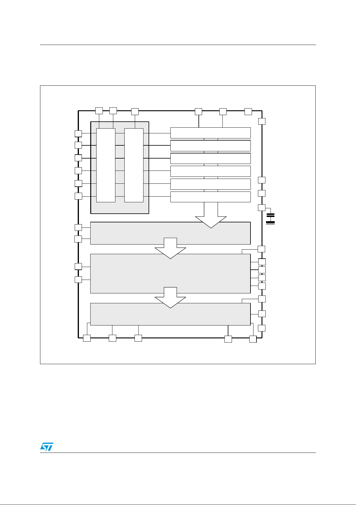
STV7622 Block diagram
DB1
DB2
DB3
DB4
DB5
DB6
BS1 BS2 DIR CLK1 CLK2 VDD
/STB1
/BLK
POC
OUT1 OUT2 OUT3 ….. …. OUT192
VSSSUB
VCC
Shift register direction
Data decoding
VSSLOG
TEST1
TEST2
VREF
10nF
RS1
RS2
FS1
FS2
Output control / EMI control
VPP
VSSP
Output buffer stage
/STB2
Latch
Q1 Q2 Q3 Q4 Q192
32-bit Shift register
32-bit Shift register
32-bit Shift register
32-bit Shift register
32-bit Shift register
32-bit Shift register
3/6/2x3-bit & RSDS
selection
1 Block diagram
Figure 2. STV7622 block diagram
3/32

Pin description STV7622
2 Pin description
Table 1. Pin description
VPP Supply DC high-voltage supply of power outputs
VCC Supply Analog 5V supply
VDD Supply Digital 5V supply
VSSP Ground Ground for power outputs
VSSSUB Ground Substrate ground
VSSLOG Ground Ground for 5V logic
OUT1 to OUT192 Outputs Power outputs
DB1to DB6 Inputs Shift register inputs
/BLK Input Blanking input
POC Input Power output control input
DIR Input Selection of shift register direction
BS1 and BS2 Inputs Shift register configuration pins (3/6/2 × 3-bits and RSDS selection)
CLK1 and CLK2 Inputs Clock for data shift register
/STB1 and /STB2 Inputs Latch of data to power outputs
RS1 and RS2 Inputs Output rise time selection pins
Pin name Function Description
FS1 and FS2 Inputs Output “slow-slope” fall time selection pins
TEST1 Test pin Must be grounded
TEST2 Test pin Must be grounded
VREF Input
Filter for internal reference - must be connected to ground via a 10nF
capacitor
Note: Inputs /BLK, /STB1 and /STB2 are active Low.
4/32

STV7622 Output stage description
VCC VPP
Output control
Totem
pole
Output 1
to 192
VSSP
OUTn
Output stage
T1
T3
Rising edge
control
Falling edge
control
T4
T2
Delay
Rise time
RS1/RS2
Fall time
FS1/FS2
VCC
3 Output stage description
Figure 3. Output stage description
5/32
Pinout description STV7622
DB6
DB5
DB4
DB3
DB2
DB1
/STB2
/STB1
CLK2
CLK1
VDD3
/BLK
VSSLOG3
POC
VDD4
DUMMY
DUMMY
VREF
DUMMY
VSSLOG4
RS1
VDD5
RS2
VSSLOG5
FS2
VDD6
FS1
VSSLOG6
DIR
VDD7
BS1
VSSLOG7
BS2
VDD8
TEST1
TEST2
DUMMY
DUMMY
DUMMY
DUMMY
DUMMY
DUMMY
DUMMY
DUMMY
VSSP1
VSSP2
VSSP3
VPP1
VPP2
VPP3
DUMMY
VSSLOG1
VSSSUB1
VDD1
VCC1
VSSP4
VSSP5
VSSP6
VPP4
VPP5
VPP6
DUMMY
VSSLOG2
VSSSUB2
VDD2
VCC2
DUMMY
OUT192
OUT191
OUT190
OUT189
OUT188
OUT187
OUT186
OUT185
OUT184
OUT183
OUT182
OUT181
OUT180
OUT12
OUT11
OUT10
OUT9
OUT8
OUT7
OUT6
OUT5
OUT4
OUT3
OUT2
OUT1
Y
X
0/0
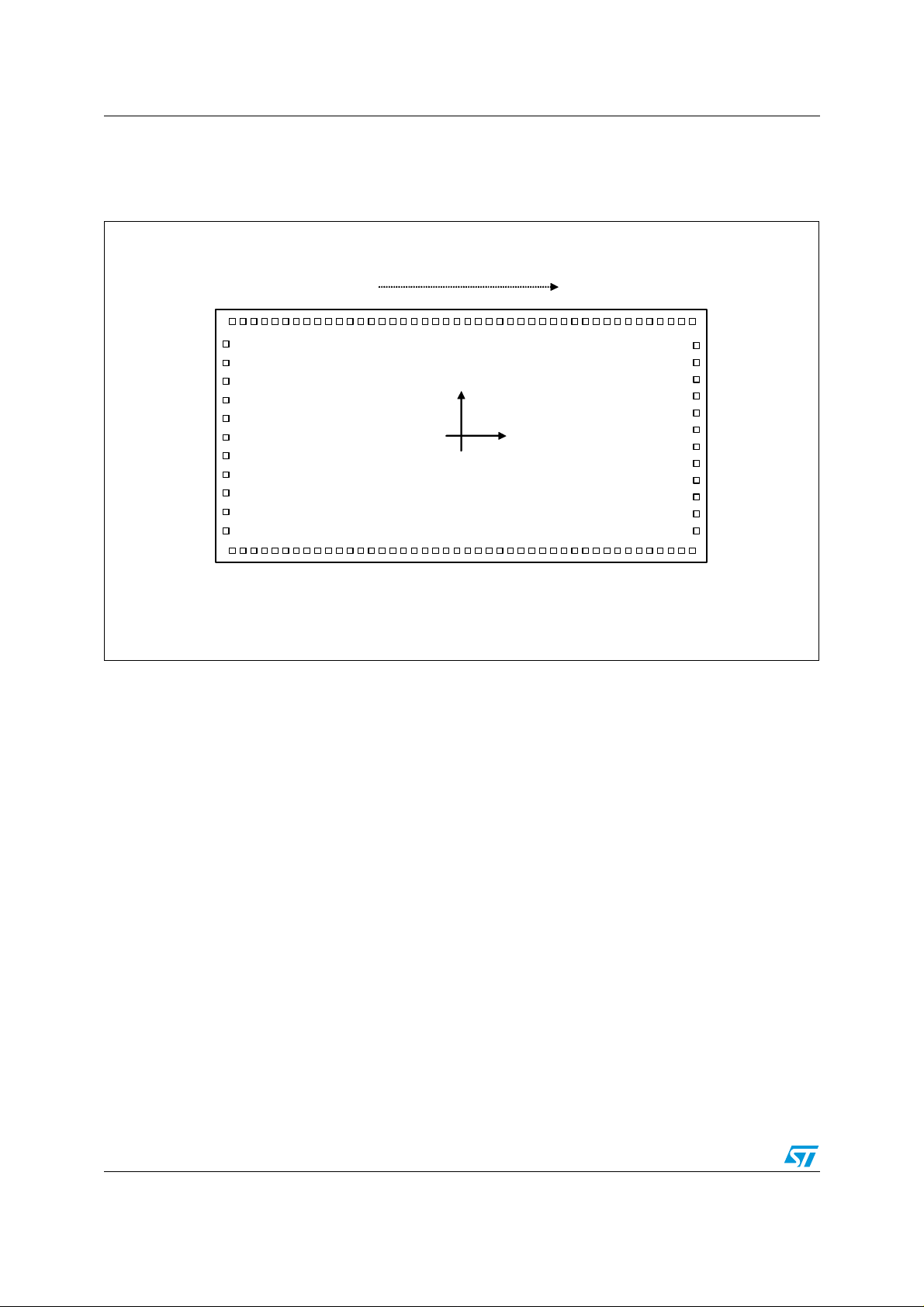
4 Pinout description
Figure 4. Pinout diagram
In the pinout diagram of Figure 4 above:
●
VDD1 to VDD8 are internally connected. It is not necessary to connect them together
on the tape carrier package (TCP) - the same applies to VCC1 and VCC2.
●
VSSLOG1 to VSSLOG2 are internally connected. It is not necessary to connect them
together on the TCP - the same for VSSSUB1 and VSSSUB2.
●
VSSLOG1 to VSSLOG7 are not internally connected to VSSSUB1 and VSSSUB2. We
recommend shorting them together very close to the die, either on the TCP or at the
TCP connector.
●
VDD1 to VDD8 are not internally connected to VCC1 and VCC2. For good test
coverage, they must not be shorted together on the TCP. In the application, VDD1 to
VDD8, VCC1 and VCC2 must be connected together at the TCP connector level.
●
TEST1 and TEST2 are used to test the device. For good test coverage, they must not
be shorted together on the TCP. In the application, TEST1 and TEST2 must be
6/32
grounded at the TCP connector level.
●
VREF must be connected to ground via a 10nF filter capacitor.

STV7622 Circuit description
5 Circuit description
The STV7622 includes all the logic and power circuits necessary to drive the column
electrodes of a Plasma Display Panel (PDP). A low-voltage logic block manages data
information, and a high-voltage block converts the low-voltage information stored in the logic
block into high-voltage signals applied to the display electrodes.
5.1 Data input block
The Data Bus is TTL- and LVCMOS-compatible and can also operate in an RSDS (Reduced
Swing Differential Signaling) mode. The maximum clock frequency is 60MHz.
The data input block consists of several shift registers operating in parallel to load the binary
values of the digital video. The number of cells in each shift register is defined by the BS pin
as described below in Table 2.
Table 2. BS1/BS2 truth table
BS1 BS2 Shift register configuration
L L 6 × 32 bits
H L 3 × 64 bits
L H RSDS mode
H H 2 × 3 × 32 bits (96 + 96)
For the 3 × 64 bit configuration, only pins DB1, DB2 and DB3 of the input data bus are used,
while for the 6 × 32 and 2 × 3 × 32 bit configurations all 6 bits of the input data bus input,
pins DB1 to DB6, are used.
The DIR input pin is used to select the shift register loading direction.
Data is shifted for each low-to-high transition of the clock signal (CLK1). The maximum
frequency of the clock is 60MHz, which is equivalent to a 360MHz serial shift register for a
6 × 32-bit arrangement.
When the /STB signal goes from high-to-low, data is transferred from the shift register to the
latch and to the power output stages. All output data is stored and held in the latch stage
when the latch input is pulled back High.
The core of the STV7622 is powered by 5V. All logic inputs can be driven either by 5V or
3.3V CMOS logic.
The tables in the following sections describe the position of the first data sampled by the first
rising edge of the CLK1 clock.
7/32

Circuit description STV7622
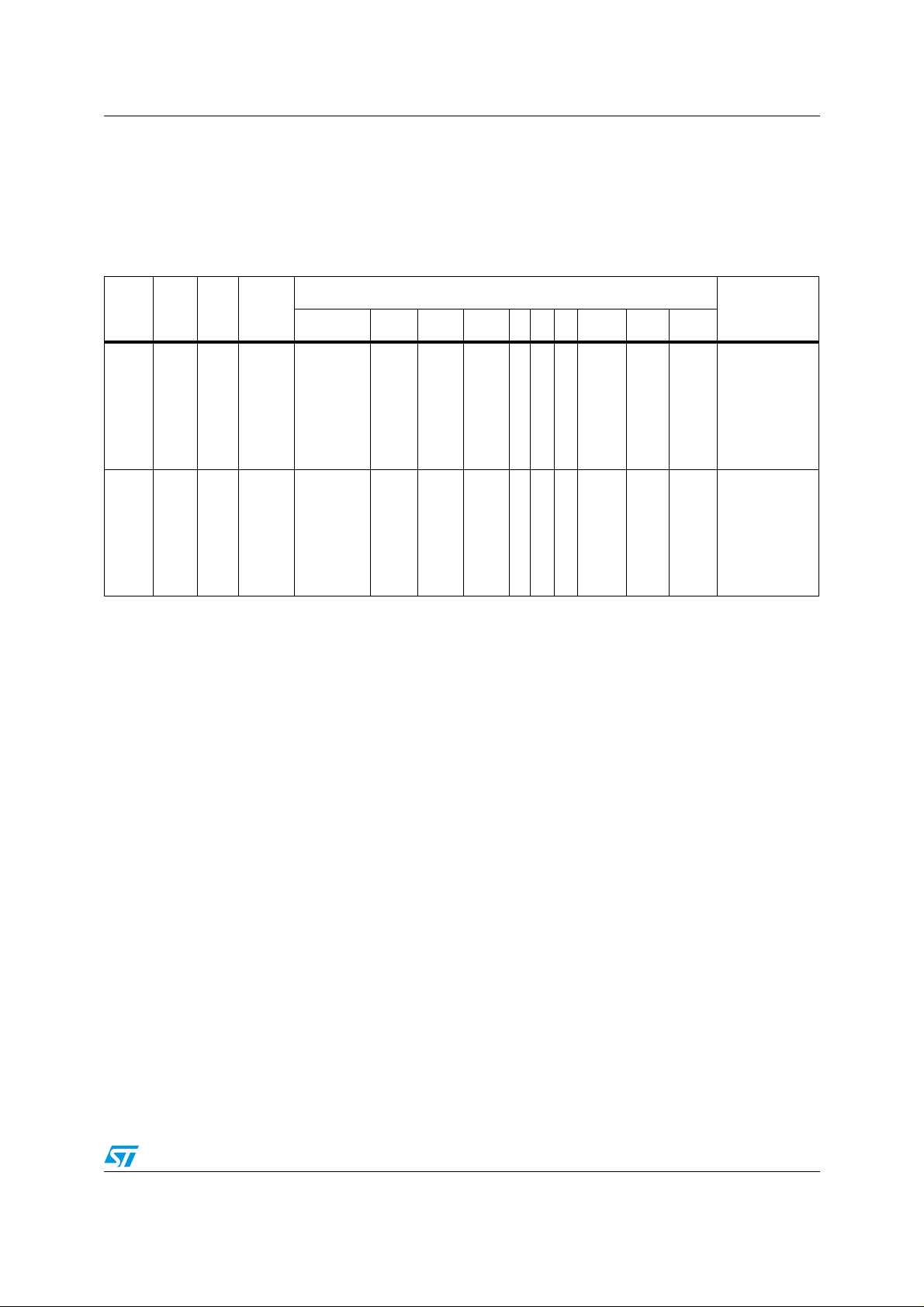
5.2 3 x 64-bit data bus, standard transmission (BS1 = H, BS2 = L)
The data bus is in 3-bit mode (DB1 to DB3 active) for BS1 = H and BS2 = L.
Data on DB1 is sampled by the first clock pulse and shifted from position 1 to position 190
after 64 clock pulses. The data is then applied to output 190, on the high-to-low transition of
/STB.
Table 3. 3 x 64-bit data bus transmission
BS1 BS2 DIR Input
Clock pulse number
Comment
Position 01 02 03 … 62 63 64
H L L
H L H
DB1
DB2
DB3
DB1
DB2
DB3
OUT
OUT
OUT
OUT
OUT
OUT
01
02
03
190
191
192
04
05
06
187
188
189
07
08
09
184
185
186
184
185
186
07
08
09
187
188
189
04
05
06
190
191
192
01
02
03
Left/Right
shift
Right/Left
shift
5.3 6 x 32-bit data bus, standard transmission (BS1 = L, BS2 = L)
The data bus is in 6-bit mode (DB1 to DB6 active) for BS1 = L and BS2 = L.
Table 4 below describes how data is shifted in the register.
Table 4. 6 x 32-bit data bus transmission
BS1 BS2 DIR Input
L L L
DB1
DB2
DB3
DB4
DB5
DB6
Position 01 02 03
Clock pulse number
OUT
OUT
OUT
OUT
OUT
OUT
01
02
03
04
05
06
07
08
09
10
11
12
13
14
15
16
17
18
…
30 31 32
175
181
187
176
182
188
177
183
189
178
184
190
179
185
191
180
186
192
Comment
Left/Right
shift
DB1
DB2
L L H
8/32
DB3
DB4
DB5
DB6
OUT
OUT
OUT
OUT
OUT
OUT
187
188
189
190
191
192
181
182
183
184
185
186
175
176
177
178
179
180
13
14
15
16
17
18
07
08
09
10
11
12
01
02
03
04
05
06
Right/Left
shift
STV7622 Circuit description
5.4 2 x 3 x 32-bit data bus, standard transmission (BS1 = H, BS2 = H)
The data bus is in 2 × 3-bit mode (DB1 to DB6 active) for BS1 = H and BS2 = H. Table 5
below describes how data is shifted in the register.
Table 5. 2 x 3 x 32-bit data bus transmission
BS1 BS2 DIR Input
Clock pulse number
Comment
Position 01 02 03
…
30 31 32
H H L
H H H
DB1
DB2
DB3
DB4
DB5
DB6
DB1
DB2
DB3
DB4
DB5
DB6
OUT
OUT
OUT
OUT
OUT
OUT
OUT
OUT
OUT
OUT
OUT
OUT
01
02
03
97
98
99
94
95
96
190
191
192
04
05
06
100
101
102
91
92
93
187
188
189
07
08
09
103
104
105
88
89
90
184
185
186
88
89
90
184
185
186
07
08
09
103
104
105
91
92
93
187
188
189
04
05
06
100
101
102
94
95
96
190
191
192
01
02
03
97
98
99
Left/Right shift
Right/Left shift
9/32
Circuit description STV7622
5.5 Differential transmission mode: RSDS (BS1 = L, BS2 = H)
In differential transmission mode, data is transmitted on two wires, one line transmits the
data value, the other the inverted data. The logic level of the data is determined by the
difference between data and inverted data. Two DB inputs are needed for the transmission
of 1 data value. The sampling clocks, CLK1 and CLK2, as well as strobes STB1/ and STB2
are also transmitted differentially. Data is sampled on the rising and falling edges of the
clock.
Table 6. 2 x 3 x 32-bit data bus transmission - differential mode
BS2 B12 DIR Input CLK1 clock pulse number Comment
H L L
H L H
In differential transmission operating mode, the biasing of the data input bus must be
carefully arranged to reduce static power consumption. In stand-by and non-active modes,
DB1, DB3, DB5, CLK1 and /STB1 should be set High to reduce bias current in the
differential input buffers.
For a High level, all differential pairs should be configured with DB1, DB3, DB5, CLK1 and
/STB1 High and with DB2, DB4, DB6, CLK2 and /STB2 Low.
When operating in differential transmission mode, a 100 ohm (1%) resistor termination must
be connected between:
●
●
●
●
●
Position 01↑ 01↓ 02↑
DB1
DB2
DB3
DB4
DB5
DB6
DB1
DB2
DB3
DB4
DB5
DB6
OUT
OUT
DB1 and DB2
DB3 and DB4
DB5 and DB6
CLK1 and CLK2
STB1 and STB2
…
01 04 07 184 187 190
02 05 08 185 188 191
03 06 09 186 189 192
190 187 184 07 04 01
191 188 185 08 05 02
192 189 186 09 06 03
31↓ 32↑ 32↓
Left/Right
shift
Right/Left
shift
with each resistor placed as close as possible to the STV7622 itself.
10/32

STV7622 Circuit description
t
PLHD
90%
10%
50%
OUTn
0 0
1.4V
1.0V
V
IA
V
IB
V
ID
10%
90%
50%
0.4V
-0.4V
t
PHLD
t
FD
t
RD
Video board
Data driver
board
DB1-DB2
DB3-DB4
DB5-DB6
CLK1-CLK2
STB1-STB2
STLVD31
STV7622
TCP
DB1-DB2
DB3-DB4
DB5-DB6
CLK1-CLK2
DB1-DB2
STLVD31
STV7622
TCP
DB1-DB2
DB3-DB4
DB5-DB6
CLK1-CLK2
DB1-DB2
STLVD31
STV7622
TCP
Display controller
100Ω
DB1-3-5
Differential
input buffer
V
0
V
IB
V
ID
DB2-4-6
(=DB1-3-5)
V
IA
Figure 5. Differential input buffer - waveform timing
11/32

Circuit description STV7622
90%
10%
t
F-SLOW
t
F-OUT
100ns01
200ns11
50ns10
10ns00
t
F-SLOW
FS1FS2
90%
10%
t
R-OUT
R
S
1
=
1
R
S
2
=
1
R
S
1
=
0
R
S
2
=
0
400ns01
560ns11
230ns10
120ns00
t
R-OUT
RS1RS2
5.6 Power output block and EMI control
The high-voltage output stage has a totem pole structure (see Figure 3). The capacitive load
is charged to Vpp by the high-side N-channel transistor, T1, and discharged to ground by
the low-side N-channel transistor, T2. The status of the power outputs can also be controlled
by the configuration pins, POC and /BLK, which can set the power outputs either all High or
all Low.
Several functions, patented by STMicroelectronics, are implemented in the STV7622 to
reduce EMI:
SmartSlope: The falling edge of the output pulse consist of 2 slopes (Figure 6 below): a
smooth slope followed by a steeper one (typically 4 times faster) The duration of the first
slope is set by two logic inputs, FS1 and FS2, according to the table in Figure 6.
Figure 6. Output falling edge
ConstantSlope: The duration of the output rising edge (Figure 7) is kept constant
independent of the value of the capacitive load connected to the output. This solution
minimizes the peak current in the power outputs as well as any oscillation phenomenon in
the power supplies. In addition, it reduces high-frequency components of the EMI spectrum
by suppressing very rapid rising edge transitions on the power outputs. The total duration of
the rising edge (t
) is set by another pair of logic inputs, RS1 and RS2, according to the
R-OUT
table in Figure 7 below.
Figure 7. Output rising edge
12/32

STV7622 Circuit description
OUT-1
OUT-x
t
SSJ-MIN
t
SSJ-MAX
OUT-1
OUT-x
Case #1: Dark picture Case #2: White picture
Spread Spectrum: To avoid having too large of a current in the driver during the rising edge
of the power outputs, all outputs are not triggered at the same time.
Instead, the STV7622 inserts a small delay between the rising edge of two consecutive
outputs. This delay depends on picture or image content (see Figure 8). For a dark picture,
we have t
SSJ-MIN
picture, we have t
= 1 to 2ns (typ.) between output 1 and any output X, while for a white
SSJ-MAX
= 100ns (typ.).
The SSJ function spreads the discharge current in the scan lines and, therefore, reduces
EMI by “spreading” the energy spectrum.
Figure 8. Spread spectrum filter
13/32

Truth tables STV7622
6 Truth tables
Table 7. Shift register truth table
Input pins Shift register function
BS2 BS1 DIR CLK1 CLK2
(1)
L L L N.C.
L L L H or L N.C. Steady
L L H N.C.
L L H H or L N.C. Steady
L H L N.C.
L H L H or L N.C. Steady
L H H N.C.
L H H H or L N.C. Steady
H L L
Q output
Left/Right shift
DB1,2,…6 input pins, 6 × 32-bit mode
Right/Left shift
DB1,2,…6 input pins, 6 × 32-bit mode
Left/Right shift
DB1,2,3 input pins, 3 × 64-bit mode
Right/Left shift
DB1,2,3 input pins, 3 × 64-bit mode
Left/Right shift
DB1,2,…6 input pins, RSDS mode
H L L H or L L or H Steady
H L H
H L H H or L L or H Steady
H H L N.C.
H H L H or L N.C. Steady
H H H N.C.
H H H H or L N.C. Steady
1. CLK2 is not used in LVCMOS operating mode and can be left “open” or “floating”.
Right/Left shift
DB1,2,…6 input pins, RSDS mode
Left/Right shift, DB1,2,… 6 input pins,
2 × 3 × 32-bit mode
Left/Right shift, DB1,2,…6 input pins,
2 × 3 × 32-bit mode
14/32

STV7622 Truth tables
Table 8. Truth table for power outputs
(1)
Q
n
/STB1 /STB2
(2)
BS1 BS2 /BLK POC
Driver
output
Note Comments
X X X X X L X all L Output at Low level
X X X X X H L all H Output at High level
X H X L L H H Q
X H L L H H H Q
X H X H L H H Q
X H X H H H H Q
L L X L L H H L
H L X L L H H H
L L H L H H H L
H L H L H H H H
L L X H L H H L
H L X H L H H H
L L X H H H H L
H L X H H H H H
n
n
n
n
(3)
Data latched
(4)
Data latched
(5)
Data latched (RSDS)
(6)
Data latched
(3)
Data copied
(3)
Data copied
(4)
Data copied (RSDS)
(4)
Data copied (RSDS)
(5)
Data copied
(5)
Data copied
(6)
Data copied
(6)
Data copied
1. Qn is the state of the shift register output (Figure 2). “X” means either High or Low (H or L).
2. /STB2 is not used in LVCMOS operating mode and can be left “open” or “floating”.
3. Q
4. RSDS mode: Q
5. Q
6. Q
n + 1
n + 1
n + 1
= DB1, Q
= DB1, Q
= DB1, Q
n + 2
n + 1
n + 2
n + 2
= DB2, Q
= DB1, Q
= DB2, Q
= DB2, Q
= DB3, Q
n + 3
= DB2, Q
n + 1
= DB3; n = {0, 3, 6, 9, … 186, 189}.
n + 3
= DB3, Q
n + 3
n + 4
n + 2
n + 97
= DB4, Q
= DB3, Q
= DB4, Q
n + 2
n + 5
n + 98
= DB5, Q
= DB4, Q
= DB5, Q
= DB6; n = {0, 6, 12, 18, … 186}.
n + 6
= DB5, Q
n + 3
n + 99
n + 3
= DB6; n = {0, 3, 6, 9, … 186, 189}.
= DB6; n = {0, 6, 12, 18, … 186}.
15/32

Absolute maximum ratings STV7622
7 Absolute maximum ratings
Table 9. Absolute maximum ratings
Symbol Parameter Value Units
Vdd Digital supply range -0.3, +7 V
Vcc Analog supply range -0.3, +7 V
Vpp Driver supply range -0.3, +90 V
Vin Logic input voltage range -0.3, Vcc+0.3 V
Ipout Driver output current x
Idout Diode output current
Vout Output power voltage range -0.3, +90 V
ESD susceptibility, Human Body Model (100pF
V
ESD
discharged through 1.5Kohms), on all except the VCC
(4)
pins
Tjmax Maximum junction temperature 100 °C
(1), (2), (3)
(1), (2), (3)
- 70/+35 mA
-200/+300 mA
2 KV
Tstg Storage temperature range -50, +150 °C
1. Measurements done on one single output, x. The other outputs are either not used or are connected to output x. Assumes
junction temperature remains less than Tjmax during measurement.
2. All transient current measurements are made under conditions close to those encountered in a typical application (that is,
with duration of any output current spike always less than 300 ns).
3. These parameters are measured during STMicroelectronics’ internal qualification which includes temperature
characterization on standard as well as corner batches of the process. These parameters are not tested in production.
4. VCC pins withstand 1.3 KV.
16/32

STV7622 Electrical characteristics
8 Electrical characteristics
VCC = VDD = 5V, VPP = 70V, VSSP = VSSLOG = VSSSUB = 0V, T
f
= 50MHz, unless otherwise specified.
CLK
Table 10. Electrical characteristics
AMB
= 25°C,
Symbol Parameter Min. Typ. Max. Units
Supply
Vdd Digital supply voltage 4.50 5 5.5 V
Idd Digital supply current
Iddl Digital Dynamic Supply Current (CLK1 freq = 20MHz)
(1)
(2)
- 10 µA
- 15 20 mA
Idd Digital Supply Current @ VIH = 2.0V 250 500 900 µA
Vcc Analog supply voltage 4.50 5 5.5 V
Icc_1 Analog supply current in standard transmission mode - 1.1 2 mA
Analog supply current in RSDS mode (that is, with
Icc_2
BS1 = BS2 = L) and with DB1, DB3, DB5, CLK1 and
/STB1 less than DB2, DB4, DB6, CLK2 and /STB2,
- 5 10 mA
respectively
Vpp DC power output supply voltage 15 80 V
Ipph-1
Ipph-2
Power output supply current (steady outputs)
@ VCC = 0V
Power output supply current (steady outputs)
@ VCC = 5V and RS1 = RS2 = L
- - 20 µA
300 450 600 µA
OUT1 to OUT192
Vpouth
Vpoutl
Vdouth
Vdoutl
Power output high level (voltage drop versus Vpp)
@ Ipouth = -20mA and Vpp = 70V
Power output low level
@ Ipoutl = +20mA
Output upper diode voltage drop
@ Idouth = +30mA (see Figure 9)
Output lower diode voltage drop
@ Idoutl = -30mA (see Figure 9)
2 3.5 5 V
3 6 10 V
- 1 2 V
-2 -1 - V
Standard Mode, TTL/LVCMOS inputs: CLK1, DIR, /STB1, POC, /BLK, BS1, BS2 and DB1 to DB6
V
IH
V
IL
I
IH
I
IL
High level input voltage 2.0 - - V
Low level input voltage - - 0.8 V
High level input current (VIH ≥ 2.0V) - - 5 µA
Low level input current (VIL = 0V) - - 5 µA
17/32

Electrical characteristics STV7622
VPP
VSSP/VSSSUB
OUTn
Idouth (*)
+
ON
OFF
Vdouth
VPP
VSSP/VSSSUB
OUTn
Idoutl (**)
-
OFF
ON
Vdoutl
(*) Output sinking current is
considered as positive.
(**) Output sourcing current is
considered as negative.
Table 10. Electrical characteristics (continued)
Symbol Parameter Min. Typ. Max. Units
RSDS Mode, inputs: CLK1, CLK2, /STB1, /STB2 and DB1 to DB6
Vid
V
ic
Cin Input capacitance
1. For 5V CMOS input logic levels (0 or 5V)
2. All input data is switched at 10MHz rate.
3. Same for TTL and RSDS modes. This parameter is measured during qualification by ST Microelectronics which includes
temperature characterization on standard as well as corner batches of the process. This parameter is not tested in
production.
Magnitude of differential input voltage 100 400 600 mV
Common mode input range 0.5Vid
(3)
- - 15 pF
1.2
2.4 −
0.5Vid
V
Figure 9. Output test configuration
18/32

STV7622 AC timing requirements
9 AC timing requirements
VCC = VDD = 4.5V to 5.5V, Tamb = -20°C to +85°C,
input signal edge maximum rise and fall times (tr, tf) = 3ns.
Table 11. AC timing requirements
Symbol Parameter Min. Typ. Max. Units
t
CLK
t
WHCLK
t
WLCLK
t
SDAT
t
HDAT
t
HSTB
t
STB
t
SSTB
Data clock period 16.7 - - ns
Duration of clock pulse at high level 8.8 - - ns
Duration of clock pulse at low level 8.8 - - ns
Input data set-up time before low-to-high clock transition 5 - - ns
Input data hold-time after low-to-high clock transition 5 - - ns
Strobe hold-time after low-to-high clock transition 5 - - ns
Duration of strobe Low level 10 - - ns
Strobe set-up time before low-to-high clock transition 5 ns
19/32

AC timing characteristics STV7622
10 AC timing characteristics
VCC = VDD = 5V, VPP = 70V, VSSP = VSSLOG = VSSSUB = 0V, Tamb = 25°C,
Fclk= 60MHz, V
Table 12. AC timing characteristics
Symbol Parameter Min Typ Max Units
t
PHL1
t
PLH1
t
PHL2
t
PLH2
t
PHL3
t
PLH3
t
R-OUT
t
R-OUT
t
R-OUT
t
R-OUT
t
F-OUT
t
F-SLOW
t
F-SLOW
t
F-SLOW
t
F-SLOW
1. t
R-OUT
2. Measurement made on one of the 192 power outputs with FS1 = “H” and FS2 = “L”. Load capacitor CL = 50pF, all other
power outputs Low.
3. t
F-SLOW
Delay of power output change after CLK1/CLK2 transition
- high to low
- low to high
Delay of power output change after /STB1/STB2
transition
- high to low
- low to high
Delay of power output change after /BLK transition
- high to low
- low to high
Power output rise time
Power output rise time
Power output rise time
Power output rise time
Power output fall time
Soft slope duration
Soft slope duration
Soft slope duration
Soft slope duration
is set externally by inputs RS1 and RS2.
is set externally by inputs FS1 and FS2.
= 0.2 × VCC, V
ILmax
(1)
(RS = “L” and RS2 = “L”)
(1)
(RS = “H” and RS2 = “L”)
(1)
(RS= “L” and RS2 = “H”)
(1)
(RS = “H” and RS2 = “H”)
(2)
(3)
(FS1 = “L” and FS2 = “L”)
(3)
(FS1 = “H” and FS2 = “L”)
(3)
(FS1 = “L” and FS2 = “H”)
(3)
(FS1 = “H” and FS2 = “H”)
= 0.8 × VCC.
IHmin
-
-
-
-
-
35
30
25
20
100
100
-
-
95
95
90
90
ns
ns
ns
ns
ns
ns
90 120 150 ns
180 230 280 ns
320 400 480 ns
470 560 670 ns
50 - 200 ns
8 10 12 ns
40 50 60 ns
80 100 120 ns
160 200 240 ns
20/32

STV7622 AC timing characteristics
t
WHCLK
50%
CLK
DB (input)
/STB
OUT(n
)
/
BLK
OUTn
50%
50%
t
WLCLK
t
CLK
50% 50%
t
SDAT
t
HDAT
50% 50%
t
STB
50%
t
HSTB
t
SSTB
90%
10%
t
PLH2
90%
10%
t
PLH1
t
PHL2
t
PHL1
50% 50%
t
PHL3
90%
10%
10%
90%
t
PLH3
t
F-OUT
t
R-OUT
(See sections on output falling/rising edge)
t
WHCLK
50%
CLK1
DB1-3-5 (input)
50%
50%
t
WLCLK
t
CLK
50% 50%
t
SDAT
t
HDAT
CLK2
DB2-4-6 (input)
Standard mode
Differential mode
50% 50%
t
STB
50%
t
HSTB
t
SSTB
/STB1
/STB2
Figure 10. AC characteristic waveforms
21/32

Pad dimensions and positions (in µm) STV7622
11 Pad dimensions and positions (in µm)
The reference (x=0, y=0) is the centre of the die. Output pad pitch is 76.5µm.
Pad placement coordinate values correspond to the center of each bump pad center. Pad
size is specified for bumping.
Table 13. Pad placement and bump pad dimensions (in microns)
Lead pad name Pad placements Bump dimensions
X Y X Y
TOP SIDE from left to right
OUT192 -7303.1 624.2 43.5 65.6
OUT191 -7226.6 624.2 43.5 65.6
OUT190 -7150.1 624.2 43.5 65.6
OUT189 -7073.6 624.2 43.5 65.6
OUT188 -6997.1 624.2 43.5 65.6
OUT187 -6920.6 624.2 43.5 65.6
OUT186 -6844.1 624.2 43.5 65.6
OUT185 -6767.6 624.2 43.5 65.6
OUT184 -6691.1 624.2 43.5 65.6
OUT183 -6614.6 624.2 43.5 65.6
OUT182 -6538.1 624.2 43.5 65.6
OUT181 -6461.6 624.2 43.5 65.6
OUT180 -6385.1 624.2 43.5 65.6
OUT179 -6308.6 624.2 43.5 65.6
OUT178 -6232.1 624.2 43.5 65.6
OUT177 -6155.6 624.2 43.5 65.6
OUT176 -6079.1 624.2 43.5 65.6
OUT175 -6002.6 624.2 43.5 65.6
OUT174 -5926.1 624.2 43.5 65.6
OUT173 -5849.6 624.2 43.5 65.6
OUT172 -5773.1 624.2 43.5 65.6
OUT171 -5696.6 624.2 43.5 65.6
OUT170 -5620.1 624.2 43.5 65.6
OUT169 -5543.6 624.2 43.5 65.6
OUT168 -5467.1 624.2 43.5 65.6
OUT167 -5390.6 624.2 43.5 65.6
OUT166 -5314.1 624.2 43.5 65.6
22/32

STV7622 Pad dimensions and positions (in µm)
Table 13. Pad placement and bump pad dimensions (in microns) (continued)
Lead pad name Pad placements Bump dimensions
X Y X Y
OUT165 -5237.6 624.2 43.5 65.6
OUT164 -5161.1 624.2 43.5 65.6
OUT163 -5084.6 624.21 43.5 65.6
OUT162 -5008.1 624.2 43.5 65.6
OUT161 -4931.6 624.2 43.5 65.6
OUT160 -4855.1 624.2 43.5 65.6
OUT159 -4778.6 624.2 43.5 65.6
OUT158 -4702.1 624.2 43.5 65.6
OUT157 -4625.6 624.2 43.5 65.6
OUT156 -4549.1 624.2 43.5 65.6
OUT155 -4472.6 624.2 43.5 65.6
OUT154 -4396.1 624.2 43.5 65.6
OUT153 -4319.6 624.2 43.5 65.6
OUT152 -4243.1 624.2 43.5 65.6
OUT151 -4166.6 624.2 43.5 65.6
OUT150 -4090.1 624.2 43.5 65.6
OUT149 -4013.6 624.2 43.5 65.6
OUT148 -3937.1 624.2 43.5 65.6
OUT147 -3860.6 624.2 43.5 65.6
OUT146 -3784.1 624.2 43.5 65.6
OUT145 -3707.6 624.2 43.5 65.6
OUT144 -3631.1 624.2 43.5 65.6
OUT143 -3554.6 624.2 43.5 65.6
OUT142 -3478.1 624.2 43.5 65.6
OUT141 -3401.6 624.2 43.5 65.6
OUT140 -3325.1 624.2 43.5 65.6
OUT139 -3248.6 624.2 43.5 65.6
OUT138 -3172.1 624.2 43.5 65.6
OUT137 -3095.6 624.2 43.5 65.6
OUT136 -3019.1 624.2 43.5 65.6
OUT135 -2942.6 624.2 43.5 65.6
OUT134 -2866.1 624.2 43.5 65.6
OUT133 -2789.6 624.2 43.5 65.6
23/32

Pad dimensions and positions (in µm) STV7622
Table 13. Pad placement and bump pad dimensions (in microns) (continued)
Lead pad name Pad placements Bump dimensions
X Y X Y
OUT132 -2713.1 624.2 43.5 65.6
OUT131 -2636.6 624.2 43.5 65.6
OUT130 -2560.1 624.2 43.5 65.6
OUT129 -2483.6 624.2 43.5 65.6
OUT128 -2407.1 624.2 43.5 65.6
OUT127 -2330.6 624.2 43.5 65.6
OUT126 -2254.1 624.215 43.5 65.6
OUT125 -2177.6 624.2 43.5 65.6
OUT124 -2101.1 624.2 43.5 65.6
OUT123 -2024.6 624.2 43.5 65.6
OUT122 -1948.1 624.2 43.5 65.6
OUT121 -1871.6 624.2 43.5 65.6
OUT120 -1795.1 624.2 43.5 65.6
OUT119 -1718.6 624.2 43.5 65.6
OUT118 -1642.1 624.2 43.5 65.6
OUT117 -1565.6 624.2 43.5 65.6
OUT116 -1489.1 624.2 43.5 65.6
OUT115 -1412.6 624.2 43.5 65.6
OUT114 -1336.1 624.2 43.5 65.6
OUT113 -1259.6 624.2 43.5 65.6
OUT112 -1183.1 624.2 43.5 65.6
OUT111 -1106.6 624.2 43.5 65.6
OUT110 -1030.1 624.2 43.5 65.6
OUT109 -953.6 624.2 43.5 65.6
OUT108 -877.1 624.2 43.5 65.6
OUT107 -800.6 624.2 43.5 65.6
OUT106 -724.1 624.2 43.5 65.6
OUT105 -647.6 624.2 43.5 65.6
OUT104 -571.1 624.2 43.5 65.6
OUT103 -494.6 624.2 43.5 65.6
OUT102 -418.1 624.2 43.5 65.6
OUT101 -341.6 624.2 43.5 65.6
OUT100 -265.1 624.2 43.5 65.6
24/32

STV7622 Pad dimensions and positions (in µm)
Table 13. Pad placement and bump pad dimensions (in microns) (continued)
Lead pad name Pad placements Bump dimensions
X Y X Y
OUT99 -188.6 624.2 43.5 65.6
OUT98 -112.1 624.2 43.5 65.6
OUT97 -35.6 624.2 43.5 65.6
OUT96 40.9 624.2 43.5 65.6
OUT95 117.4 624.2 43.5 65.6
OUT94 193.9 624.2 43.5 65.6
OUT93 270.4 624.2 43.5 65.6
OUT92 346.9 624.2 43.5 65.6
OUT91 423.4 624.2 43.5 65.6
OUT90 499.9 624.2 43.5 65.6
OUT89 576.4 624.2 43.5 65.6
OUT88 652.9 624.2 43.5 65.6
OUT87 729.4 624.2 43.5 65.6
OUT86 805.9 624.2 43.5 65.6
OUT85 882.4 624.2 43.5 65.6
OUT84 958.9 624.2 43.5 65.6
OUT83 1035.4 624.2 43.5 65.6
OUT82 1111.9 624.2 43.5 65.6
OUT81 1188.4 624.2 43.5 65.6
OUT80 1264.9 624.2 43.5 65.6
OUT79 1341.4 624.2 43.5 65.6
OUT78 1417.9 624.2 43.5 65.6
OUT77 1494.4 624.2 43.5 65.6
OUT76 1570.9 624.2 43.5 65.6
OUT75 1647.4 624.2 43.5 65.6
OUT74 1723.9 624.2 43.5 65.6
OUT73 1800.4 624.2 43.5 65.6
OUT72 1876.9 624.2 43.5 65.6
OUT71 1953.4 624.2 43.5 65.6
OUT70 2029.9 624.2 43.5 65.6
OUT69 2106.4 624.2 43.5 65.6
OUT68 2182.9 624.2 43.5 65.6
OUT67 2259.4 624.2 43.5 65.6
25/32

Pad dimensions and positions (in µm) STV7622
Table 13. Pad placement and bump pad dimensions (in microns) (continued)
Lead pad name Pad placements Bump dimensions
X Y X Y
OUT66 2335.8 624.2 43.5 65.6
OUT65 2412.3 624.2 43.5 65.6
OUT64 2488.9 624.2 43.5 65.6
OUT63 2565.4 624.2 43.5 65.6
OUT62 2641.9 624.2 43.5 65.6
OUT61 2718.4 624.2 43.5 65.6
OUT60 2794.9 624.2 43.5 65.6
OUT59 2871.4 624.2 43.5 65.6
OUT58 2947.9 624.2 43.5 65.6
OUT57 3024.4 624.2 43.5 65.6
OUT56 3100.9 624.2 43.5 65.6
OUT55 3177.4 624.2 43.5 65.6
OUT54 3253.9 624.2 43.5 65.6
OUT53 3330.4 624.2 43.5 65.6
OUT52 3406.9 624.2 43.5 65.6
OUT51 3483.4 624.2 43.5 65.6
OUT50 3559.9 624.2 43.5 65.6
OUT49 3636.4 624.2 43.5 65.6
OUT48 3712.9 624.2 43.5 65.6
OUT47 3789.4 624.2 43.5 65.6
OUT46 3865.9 624.2 43.5 65.6
OUT45 3942.4 624.2 43.5 65.6
OUT44 4018.9 624.2 43.5 65.6
OUT43 4095.4 624.2 43.5 65.6
OUT42 4171.9 624.2 43.5 65.6
OUT41 4248.4 624.2 43.5 65.6
OUT40 4324.9 624.2 43.5 65.6
OUT39 4401.4 624.2 43.5 65.6
OUT38 4477.9 624.2 43.5 65.6
OUT37 4554.4 624.2 43.5 65.6
OUT36 4630.9 624.2 43.5 65.6
OUT35 4707.4 624.2 43.5 65.6
OUT34 4783.9 624.2 43.5 65.6
26/32

STV7622 Pad dimensions and positions (in µm)
Table 13. Pad placement and bump pad dimensions (in microns) (continued)
Lead pad name Pad placements Bump dimensions
X Y X Y
OUT33 4860.4 624.2 43.5 65.6
OUT32 4936.9 624.2 43.5 65.6
OUT31 5013.4 624.2 43.5 65.6
OUT30 5089.9 624.2 43.5 65.6
OUT29 5166.4 624.2 43.5 65.6
OUT28 5242.9 624.2 43.5 65.6
OUT27 5319.4 624.2 43.5 65.6
OUT26 5395.9 624.2 43.5 65.6
OUT25 5472.4 624.2 43.5 65.6
OUT24 5548.9 624.2 43.5 65.6
OUT23 5625.4 624.2 43.5 65.6
OUT22 5701.9 624.2 43.5 65.6
OUT21 5778.4 624.2 43.5 65.6
OUT20 5854.9 624.2 43.5 65.6
OUT19 5931.4 624.2 43.5 65.6
OUT18 6007.9 624.2 43.5 65.6
OUT17 6084.4 624.2 43.5 65.6
OUT16 6160.9 624.2 43.5 65.6
OUT15 6237.4 624.2 43.5 65.6
OUT14 6313.9 624.2 43.5 65.6
OUT13 6390.4 624.2 43.5 65.6
OUT12 6466.9 624.2 43.5 65.6
OUT11 6543.4 624.2 43.5 65.6
OUT10 6619.9 624.2 43.5 65.6
OUT9 6696.4 624.2 43.5 65.6
OUT8 6772.9 624.2 43.5 65.6
OUT7 6849.4 624.2 43.5 65.6
OUT6 6925.9 624.2 43.5 65.6
OUT5 7002.4 624.2 43.5 65.6
OUT4 7078.9 624.2 43.5 65.6
OUT3 7155.4 624.2 43.5 65.6
OUT2 7231.9 624.2 43.5 65.6
OUT1 7308.4 624.2 43.5 65.6
27/32

Pad dimensions and positions (in µm) STV7622
Table 13. Pad placement and bump pad dimensions (in microns) (continued)
Lead pad name Pad placements Bump dimensions
X Y X Y
RIGHT SIDE from top to bottom
VSSP4 7461.3 635.2 65.6 43.5
VSSP5 7473.2 560.3 65.6 43.5
VSSP6 7473.2 485.4 65.6 43.5
VPP4 7473.2 260.1 65.6 43.5
VPP5 7473.2 185.2 65.6 43.5
VPP6 7473.2 110.3 65.6 43.5
DUMMY 7473.2 35.5 65.6 43.5
VSSLOG2 7473.2 -39.4 65.6 43.5
VSSSUB2 7473.2 -114.3 65.6 43.5
VDD2 7473.2 -189.2 65.6 43.5
VCC2 7473.2 -555.2 65.6 43.5
DUMMY 7461.3 -633.5 65.6 43.5
BOTTOM SIDE from right to left
DUMMY 6838.2 -622.5 43.5 65.6
DUMMY 6749.7 -622.5 43.5 65.6
DUMMY 6673.1 -622.5 43.5 65.6
DUMMY 6486.3 -622.5 43.5 65.6
DUMMY 6409.8 -622.5 43.5 65.6
DUMMY 6333.3 -622.5 43.5 65.6
DUMMY 6256.8 -622.5 43.5 65.6
DUMMY 6103.6 -622.5 43.5 65.6
TEST2 5928.9 -622.5 43.5 65.6
TEST1 5617.8 -622.5 43.5 65.6
VDD8 4783.9 -622.5 43.5 65.6
BS2 4634.4 -622.5 43.5 65.6
VSSLOG7 4466.3 -622.5 43.5 65.6
BS1 4325.9 -622.5 43.5 65.6
VDD7 4095.4 -622.5 43.5 65.6
DIR 3949.6 -622.5 43.5 65.6
VSSLOG6 3709.5 -622.5 43.5 65.6
FS1 3560.2 -622.5 43.5 65.6
VDD6 3327.0 -622.5 43.5 65.6
28/32

STV7622 Pad dimensions and positions (in µm)
Table 13. Pad placement and bump pad dimensions (in microns) (continued)
Lead pad name Pad placements Bump dimensions
X Y X Y
FS2 3178.1 -622.5 43.5 65.6
VSSLOG5 2944.5 -622.5 43.5 65.6
RS2 2798.8 -622.5 43.5 65.6
VDD5 2629.4 -622.5 43.5 65.6
RS1 2486.6 -622.5 43.5 65.6
VSSLOG4 2314.1 -622.5 43.5 65.6
DUMMY 648.6 -622.5 43.5 65.6
VREF 117.6 -622.5 43.5 65.6
DUMMY -271.1 -622.5 43.5 65.6
DUMMY -424.1 -622.5 43.5 65.6
VDD4 -572.067 -622.5 43.5 65.6
POC -870.5 -622.5 43.5 65.6
VSSLOG3 -1110.0 -622.5 43.5 65.6
BLK/ -1458.1 -622.5 43.5 65.6
VDD3 -1722.0 -622.5 43.5 65.6
CLK1 -1958.7 -622.5 43.5 65.6
CLK2 -2567.3 -622.5 43.5 65.6
STB1/ -3018.9 -622.5 43.5 65.6
STB2/ -3561.8 -622.5 43.5 65.6
DB1 -4021.4 -622.5 43.5 65.6
DB2 -4632.8 -622.5 43.5 65.6
DB3 -5015.9 -622.5 43.5 65.6
DB4 -5840.8 -622.5 43.5 65.6
DB5 -6114.5 -622.5 43.5 65.6
DB6 -7094.6 -622.5 43.5 65.6
29/32

Pad dimensions and positions (in µm) STV7622
Table 13. Pad placement and bump pad dimensions (in microns) (continued)
Lead pad name Pad placements Bump dimensions
X Y X Y
LEFT SIDE from bottom to top
VCC1 -7474.9 -555.2 65.6 43.5
VDD1 -7474.9 -189.2 65.6 43.5
VSSSUB1 -7474.9 -114.3 65.6 43.5
VSSLOG1 -7474.9 -39.4 65.6 43.5
DUMMY -7474.9 35.5 65.6 43.5
VPP3 -7474.9 110.3 65.6 43.5
VPP2 -7474.9 185.2 65.6 43.5
VPP1 -7474.9 260.1 65.6 43.5
VSSP3 -7474.9 485.5 65.6 43.5
VSSP2 -7474.9 560.3 65.6 43.5
VSSP1 -7462.9 635.2 65.6 43.5
30/32

STV7622 Tested wafer disclaimer
12 Tested wafer disclaimer
All wafers are tested and guaranteed to comply with this specification until the wafer sawing
stage, for a period of ninety (90) days from the delivery date.
Please remember that it is the customer’s responsibility to test and qualify their application
using the STMicroelectronics die. STMicroelectronics is ready to support customers when
qualifying the product.
13 Ordering information
Table 14. Order codes
Part number Description
STV7622/BMP Tested and usawn bump wafer (u = die)
14 Revision history
Table 15. Document revision history
Date Revision Changes
29-May-2007 1 Initial release
31/32

STV7622
Please Read Carefully:
Information in this document is provided solely in connection with ST products. STMicroelectronics NV and its subsidiaries (“ST”) reserve the
right to make changes, corrections, modifications or improvements, to this document, and the products and services described herein at any
time, without notice.
All ST products are sold pursuant to ST’s terms and conditions of sale.
Purchasers are solely responsible for the choice, selection and use of the ST products and services described herein, and ST assumes no
liability whatsoever relating to the choice, selection or use of the ST products and services described herein.
No license, express or implied, by estoppel or otherwise, to any intellectual property rights is granted under this document. If any part of this
document refers to any third party products or services it shall not be deemed a license grant by ST for the use of such third party products
or services, or any intellectual property contained therein or considered as a warranty covering the use in any manner whatsoever of such
third party products or services or any intellectual property contained therein.
UNLESS OTHERWISE SET FORTH IN ST’S TERMS AND CONDITIONS OF SALE ST DISCLAIMS ANY EXPRESS OR IMPLIED
WARRANTY WITH RESPECT TO THE USE AND/OR SALE OF ST PRODUCTS INCLUDING WITHOUT LIMITATION IMPLIED
WARRANTIES OF MERCHANTABILITY, FITNESS FOR A PARTICULAR PURPOSE (AND THEIR EQUIVALENTS UNDER THE LAWS
OF ANY JURISDICTION), OR INFRINGEMENT OF ANY PATENT, COPYRIGHT OR OTHER INTELLECTUAL PROPERTY RIGHT.
UNLESS EXPRESSLY APPROVED IN WRITING BY AN AUTHORIZED ST REPRESENTATIVE, ST PRODUCTS ARE NOT
RECOMMENDED, AUTHORIZED OR WARRANTED FOR USE IN MILITARY, AIR CRAFT, SPACE, LIFE SAVING, OR LIFE SUSTAINING
APPLICATIONS, NOR IN PRODUCTS OR SYSTEMS WHERE FAILURE OR MALFUNCTION MAY RESULT IN PERSONAL INJURY,
DEATH, OR SEVERE PROPERTY OR ENVIRONMENTAL DAMAGE. ST PRODUCTS WHICH ARE NOT SPECIFIED AS "AUTOMOTIVE
GRADE" MAY ONLY BE USED IN AUTOMOTIVE APPLICATIONS AT USER’S OWN RISK.
Resale of ST products with provisions different from the statements and/or technical features set forth in this document shall immediately void
any warranty granted by ST for the ST product or service described herein and shall not create or extend in any manner whatsoever, any
liability of ST.
ST and the ST logo are trademarks or registered trademarks of ST in various countries.
Information in this document supersedes and replaces all information previously supplied.
The ST logo is a registered trademark of STMicroelectronics. All other names are the property of their respective owners.
© 2007 STMicroelectronics - All rights reserved
STMicroelectronics group of companies
Australia - Belgium - Brazil - Canada - China - Czech Republic - Finland - France - Germany - Hong Kong - India - Israel - Italy - Japan -
Malaysia - Malta - Morocco - Singapore - Spain - Sweden - Switzerland - United Kingdom - United States of America
www.st.com
32/32
 Loading...