

Page 1

Programmable poly-phase energy calculator IC
Features
■ Supports 1-, 2- or 3-phase WYE and Delta
services, from 2 to 4 wires
■ Computes cumulative active and reactive wide-
band and fundamental harmonic energies
■ Computes active and reactive energies, RMS
and momentary voltage and current values for
each phase
■ Supports Rogowski coil, current transformer,
Shunt or Hall current sensors
■ Exclusive ripple-free energy calculation
algorithm
■ Programmable pulsed output
■ Stepper motor outputs
■ Neutral current, temperature, and magnetic
field monitoring
■ OTP memory for configuration and calibration
■ SPI interface
■ Supports IEC 62052-11 / 62053-21 / 62053-23
standards
■ Less than 0.1 % error over 1:1000 dynamic
range
Applications
■ Power metering
Description
The STPMC1 device functions as an energy
calculator and is an ASSP designed for effective
energy measurement in power line systems
utilizing Rogowski, current transformer, Shunt or
Hall current sensors. Used in combination with
one or more STPMSx ICs, it implements all the
functions needed in a 1-, 2- or 3-phase energy
Table 1. Device summary
Order code Temperature range Package Packaging
STPMC1
Datasheet − production data
TSSOP20
meter. It can be coupled with a microprocessor for
multi-function energy meters, or it can directly
drive a stepper motor for a simple active energy
meter. The calculator has five input data pins. The
first three receive the voltage and current
information of the phases. In fact, each data input
processes two ΔΣ signals, multiplexed in time and
generated by the STPMSx device. The fourth
input receives multiplexed ΔΣ signals also, and
can be used to sense the neutral current or
another signal - temperature, for example. The
fifth input data pin accepts non-multiplexed ΔΣ
signals and it can be used for sensing the
magnetic field information from a Hall sensor.
Four internal hard-wired DSP (digital signal
processing) units perform all the computations on
the ΔΣ streams in real time by means of ΔΣ
arithmetic blocks. This allows the achievement of
very high computation precision with fast and
efficient digital architecture. All the data recorded
by the STPMC1 are accessible through an SPI
port, which is also used to configure and calibrate
the device. The configuration and calibration data
can be saved in a 112-bit OTP block, or
dynamically set in microprocessor-based meters.
STPMC1BTR - 40 to 85 °C TSSOP20 (tape and reel) 2500 parts per reel
April 2012 Doc ID 15728 Rev 6 1/77
This is information on a product in full production.
www.st.com
77
Page 2

Contents STPMC1
Contents
1 Functional block diagram . . . . . . . . . . . . . . . . . . . . . . . . . . . . . . . . . . . . . 5
2 Pin configuration . . . . . . . . . . . . . . . . . . . . . . . . . . . . . . . . . . . . . . . . . . . 6
3 Maximum ratings . . . . . . . . . . . . . . . . . . . . . . . . . . . . . . . . . . . . . . . . . . . . 8
4 Functions . . . . . . . . . . . . . . . . . . . . . . . . . . . . . . . . . . . . . . . . . . . . . . . . . . 9
5 Application . . . . . . . . . . . . . . . . . . . . . . . . . . . . . . . . . . . . . . . . . . . . . . . . 10
6 Electrical characteristics . . . . . . . . . . . . . . . . . . . . . . . . . . . . . . . . . . . . 12
7 Terminology . . . . . . . . . . . . . . . . . . . . . . . . . . . . . . . . . . . . . . . . . . . . . . . 14
7.1 Measurement error . . . . . . . . . . . . . . . . . . . . . . . . . . . . . . . . . . . . . . . . . . 14
7.2 Conventions . . . . . . . . . . . . . . . . . . . . . . . . . . . . . . . . . . . . . . . . . . . . . . . 14
7.3 Notation . . . . . . . . . . . . . . . . . . . . . . . . . . . . . . . . . . . . . . . . . . . . . . . . . . 14
8 Typical performance characteristics . . . . . . . . . . . . . . . . . . . . . . . . . . . 16
9 Theory of operation . . . . . . . . . . . . . . . . . . . . . . . . . . . . . . . . . . . . . . . . 18
9.1 General operation . . . . . . . . . . . . . . . . . . . . . . . . . . . . . . . . . . . . . . . . . . . 18
9.2 Power supply . . . . . . . . . . . . . . . . . . . . . . . . . . . . . . . . . . . . . . . . . . . . . . 20
9.3 Resetting the STPMC1 (status bit HLT) . . . . . . . . . . . . . . . . . . . . . . . . . . 21
9.4 Clock generator (bits MDIV, FR1, HSA) . . . . . . . . . . . . . . . . . . . . . . . . . . 21
9.5 Zero crossing detection (signal ZCR) . . . . . . . . . . . . . . . . . . . . . . . . . . . . 23
9.6 Period and line voltage measurement (status bits: LIN, BFR, LOW, BFF) 23
9.7 Single wire operation mode: SWM (status bits: NAH, BFR,
configuration bit FRS) . . . . . . . . . . . . . . . . . . . . . . . . . . . . . . . . . . . . . . . . 25
9.8 Load monitoring (status bit BIL, configuration bit LTCH) . . . . . . . . . . . . . 26
9.9 Error detection (status bits: BCF, PIN) . . . . . . . . . . . . . . . . . . . . . . . . . . . 27
9.10 Tamper detection module (status bits: BCS, BSF, BIF,
configuration bit ENH) . . . . . . . . . . . . . . . . . . . . . . . . . . . . . . . . . . . . . . . 27
9.10.1 Sum of currents is above tamper threshold (status bit BCS) . . . . . . . . . 28
9.10.2 Phase sequence is wrong (status bit BSF) . . . . . . . . . . . . . . . . . . . . . . 31
9.10.3 Phase active powers do not have the same sign (status bit BIF) . . . . . 32
2/77 Doc ID 15728 Rev 6
Page 3

STPMC1 Contents
9.10.4 EMI is detected . . . . . . . . . . . . . . . . . . . . . . . . . . . . . . . . . . . . . . . . . . . 32
9.11 Energy to frequency conversion (configuration bits: APL, KMOT,
LVS, FUND) . . . . . . . . . . . . . . . . . . . . . . . . . . . . . . . . . . . . . . . . . . . . . . . 32
9.12 Using STPMC1 in microcontroller based meter - peripheral
operating mode (configuration bits: APL, KMOT, LVS, FUND) . . . . . . . . . 34
9.13 Driving a stepper motor - standalone operating mode
(configuration bits: APL, LVS, KMOT) . . . . . . . . . . . . . . . . . . . . . . . . . . . 35
9.14 Negative power accumulation (configuration bit ABS, status bit SIGN) . . 37
9.15 Phase delay calculation . . . . . . . . . . . . . . . . . . . . . . . . . . . . . . . . . . . . . . 37
9.16 Calibration (configuration bits: PM, TCS, CIX, CVX, CCA, CCB, CPX) . . 40
9.16.1 Voltage and current channels calibration . . . . . . . . . . . . . . . . . . . . . . . . 40
9.16.2 Phase compensation . . . . . . . . . . . . . . . . . . . . . . . . . . . . . . . . . . . . . . . 40
9.16.3 Mutual current compensation . . . . . . . . . . . . . . . . . . . . . . . . . . . . . . . . 44
9.17 Data records map . . . . . . . . . . . . . . . . . . . . . . . . . . . . . . . . . . . . . . . . . . . 46
9.17.1 Group 0 data records . . . . . . . . . . . . . . . . . . . . . . . . . . . . . . . . . . . . . . . 46
9.17.2 Group 1 data records . . . . . . . . . . . . . . . . . . . . . . . . . . . . . . . . . . . . . . . 47
9.17.3 Group 2 data records . . . . . . . . . . . . . . . . . . . . . . . . . . . . . . . . . . . . . . . 48
9.17.4 Group 3 data records . . . . . . . . . . . . . . . . . . . . . . . . . . . . . . . . . . . . . . . 49
9.17.5 Group 4 data records . . . . . . . . . . . . . . . . . . . . . . . . . . . . . . . . . . . . . . . 50
9.17.6 Group 5 data records . . . . . . . . . . . . . . . . . . . . . . . . . . . . . . . . . . . . . . . 51
9.17.7 Group 6 data records . . . . . . . . . . . . . . . . . . . . . . . . . . . . . . . . . . . . . . . 52
9.17.8 Parity calculation . . . . . . . . . . . . . . . . . . . . . . . . . . . . . . . . . . . . . . . . . . 52
9.18 Status bits map . . . . . . . . . . . . . . . . . . . . . . . . . . . . . . . . . . . . . . . . . . . . . 53
9.19 Configuration bits map . . . . . . . . . . . . . . . . . . . . . . . . . . . . . . . . . . . . . . . 54
9.20 Mode signals . . . . . . . . . . . . . . . . . . . . . . . . . . . . . . . . . . . . . . . . . . . . . . 59
9.21 SPI interface (configuration bit SCLP) . . . . . . . . . . . . . . . . . . . . . . . . . . . 60
9.21.1 Remote reset . . . . . . . . . . . . . . . . . . . . . . . . . . . . . . . . . . . . . . . . . . . . . 61
9.21.2 Reading data records . . . . . . . . . . . . . . . . . . . . . . . . . . . . . . . . . . . . . . 62
9.21.3 Writing procedure . . . . . . . . . . . . . . . . . . . . . . . . . . . . . . . . . . . . . . . . . 63
9.21.4 Interfacing the standard 3-wire SPI with STPMC1 SPI . . . . . . . . . . . . . 65
9.21.5 Permanent writing of the CFG bits . . . . . . . . . . . . . . . . . . . . . . . . . . . . . 65
10 Energy calculation algorithm . . . . . . . . . . . . . . . . . . . . . . . . . . . . . . . . . 67
10.1 Active energy calculation . . . . . . . . . . . . . . . . . . . . . . . . . . . . . . . . . . . . . 68
10.2 Reactive energy calculation . . . . . . . . . . . . . . . . . . . . . . . . . . . . . . . . . . . 69
10.3 Voltage and current RMS values calculation . . . . . . . . . . . . . . . . . . . . . . 71
Doc ID 15728 Rev 6 3/77
Page 4

Contents STPMC1
10.4 Energy integration . . . . . . . . . . . . . . . . . . . . . . . . . . . . . . . . . . . . . . . . . . 71
10.5 Fundamental power calculation . . . . . . . . . . . . . . . . . . . . . . . . . . . . . . . . 72
11 Package mechanical data . . . . . . . . . . . . . . . . . . . . . . . . . . . . . . . . . . . . 73
12 Revision history . . . . . . . . . . . . . . . . . . . . . . . . . . . . . . . . . . . . . . . . . . . 76
4/77 Doc ID 15728 Rev 6
Page 5

STPMC1 List of tables
List of tables
Table 1. Device summary . . . . . . . . . . . . . . . . . . . . . . . . . . . . . . . . . . . . . . . . . . . . . . . . . . . . . . . . . . 1
Table 2. Pin description . . . . . . . . . . . . . . . . . . . . . . . . . . . . . . . . . . . . . . . . . . . . . . . . . . . . . . . . . . . 8
Table 3. Absolute maximum ratings . . . . . . . . . . . . . . . . . . . . . . . . . . . . . . . . . . . . . . . . . . . . . . . . . . 9
Table 4. Thermal data. . . . . . . . . . . . . . . . . . . . . . . . . . . . . . . . . . . . . . . . . . . . . . . . . . . . . . . . . . . . . 9
Table 5. Programmable pin functions . . . . . . . . . . . . . . . . . . . . . . . . . . . . . . . . . . . . . . . . . . . . . . . . 10
Table 6. Typical external components . . . . . . . . . . . . . . . . . . . . . . . . . . . . . . . . . . . . . . . . . . . . . . . 12
Table 7. Electrical characteristics . . . . . . . . . . . . . . . . . . . . . . . . . . . . . . . . . . . . . . . . . . . . . . . . . . . 13
Table 8. Notation . . . . . . . . . . . . . . . . . . . . . . . . . . . . . . . . . . . . . . . . . . . . . . . . . . . . . . . . . . . . . . . 16
Table 9. Input channels from the STPMSx . . . . . . . . . . . . . . . . . . . . . . . . . . . . . . . . . . . . . . . . . . . . 19
Table 10. Frequency settings through MDIV and FR1 . . . . . . . . . . . . . . . . . . . . . . . . . . . . . . . . . . . 23
Table 11. CLK pin frequency settings through HSA . . . . . . . . . . . . . . . . . . . . . . . . . . . . . . . . . . . . . . 23
Table 12. STPMC1 configuration for STPMS2 . . . . . . . . . . . . . . . . . . . . . . . . . . . . . . . . . . . . . . . . . . 23
Table 13. Good frequency ranges for different clock source values. . . . . . . . . . . . . . . . . . . . . . . . . . 24
Table 14. No-load detection thresholds . . . . . . . . . . . . . . . . . . . . . . . . . . . . . . . . . . . . . . . . . . . . . . . 27
Table 15. Tamper conditions . . . . . . . . . . . . . . . . . . . . . . . . . . . . . . . . . . . . . . . . . . . . . . . . . . . . . . . 29
Table 16. Pin description versus SYS configuration (uX and iX represent the voltage
and the current signals) . . . . . . . . . . . . . . . . . . . . . . . . . . . . . . . . . . . . . . . . . . . . . . . . . . . 32
Table 17. Energy registers LSB value . . . . . . . . . . . . . . . . . . . . . . . . . . . . . . . . . . . . . . . . . . . . . . . . 33
Table 18. LED pin configuration for APL = 0 . . . . . . . . . . . . . . . . . . . . . . . . . . . . . . . . . . . . . . . . . . . 35
Table 19. LED pin configuration for APL = 1 . . . . . . . . . . . . . . . . . . . . . . . . . . . . . . . . . . . . . . . . . . . 35
Table 20. Configuration of MOP and MON driving signals with APL = 1, 2, 3 . . . . . . . . . . . . . . . . . . 36
Table 21. LED pin configuration for APL = 2, 3 . . . . . . . . . . . . . . . . . . . . . . . . . . . . . . . . . . . . . . . . . 37
Table 22. Accumulation mode for negative power . . . . . . . . . . . . . . . . . . . . . . . . . . . . . . . . . . . . . . . 37
Table 23. f
Table 24. f
Table 25. f
Table 26. Phase compensation for PM = 0, TCS = 0, fline = 50 Hz . . . . . . . . . . . . . . . . . . . . . . . . . . 42
Table 27. Phase compensation for PM = 0, TCS = 1, fline = 50 Hz . . . . . . . . . . . . . . . . . . . . . . . . . . 43
Table 28. Phase compensation for PM = 1, fline = 50 Hz . . . . . . . . . . . . . . . . . . . . . . . . . . . . . . . . . 44
Table 29. Mutual current compensation matrix for single-phase systems (SYS > 3) . . . . . . . . . . . . . 45
Table 30. Mutual current compensation matrix for three-phase systems (SYS < 4) . . . . . . . . . . . . . 45
Table 31. 3-phase status bits description . . . . . . . . . . . . . . . . . . . . . . . . . . . . . . . . . . . . . . . . . . . . . . 53
Table 32. X-phase status bits description . . . . . . . . . . . . . . . . . . . . . . . . . . . . . . . . . . . . . . . . . . . . . . 54
Table 33. Configuration bits map . . . . . . . . . . . . . . . . . . . . . . . . . . . . . . . . . . . . . . . . . . . . . . . . . . . . 55
Table 34. Mode signals description . . . . . . . . . . . . . . . . . . . . . . . . . . . . . . . . . . . . . . . . . . . . . . . . . . 59
Table 35. Functional description of commands . . . . . . . . . . . . . . . . . . . . . . . . . . . . . . . . . . . . . . . . . 64
Table 36. Document revision history . . . . . . . . . . . . . . . . . . . . . . . . . . . . . . . . . . . . . . . . . . . . . . . . . 76
frequency settings . . . . . . . . . . . . . . . . . . . . . . . . . . . . . . . . . . . . . . . . . . . . . . . . . . . . 41
phc
frequency values . . . . . . . . . . . . . . . . . . . . . . . . . . . . . . . . . . . . . . . . . . . . . . . . . . . . . 41
phc
frequency settings for PM = 1 . . . . . . . . . . . . . . . . . . . . . . . . . . . . . . . . . . . . . . . . . . . 41
phc
Doc ID 15728 Rev 6 5/77
Page 6

List of figures STPMC1
List of figures
Figure 1. STPMC1 device block diagram . . . . . . . . . . . . . . . . . . . . . . . . . . . . . . . . . . . . . . . . . . . . . . 7
Figure 2. Pin connections (top view) . . . . . . . . . . . . . . . . . . . . . . . . . . . . . . . . . . . . . . . . . . . . . . . . . . 8
Figure 3. Application schematic in standalone operating mode. . . . . . . . . . . . . . . . . . . . . . . . . . . . . 11
Figure 4. Application schematic using an MCU . . . . . . . . . . . . . . . . . . . . . . . . . . . . . . . . . . . . . . . . . 11
Figure 5. Supply current vs. supply voltage, T
Figure 6. Digital voltage regulator: line - load regulation. (f
across V
and VSS; 1 µF across VDD and V
CC
Figure 7. Gain response of decimator . . . . . . . . . . . . . . . . . . . . . . . . . . . . . . . . . . . . . . . . . . . . . . . . 18
Figure 8. Connections of oscillator: (a) quartz, (b) external source . . . . . . . . . . . . . . . . . . . . . . . . . . 22
Figure 9. ZCR signal . . . . . . . . . . . . . . . . . . . . . . . . . . . . . . . . . . . . . . . . . . . . . . . . . . . . . . . . . . . . . 24
Figure 10. LIN and BFR behavior when f
line
Figure 11. Currents of the three phase system in example . . . . . . . . . . . . . . . . . . . . . . . . . . . . . . . . . 30
Figure 12. Stepper driving signals . . . . . . . . . . . . . . . . . . . . . . . . . . . . . . . . . . . . . . . . . . . . . . . . . . . . 36
Figure 13. Phase delay . . . . . . . . . . . . . . . . . . . . . . . . . . . . . . . . . . . . . . . . . . . . . . . . . . . . . . . . . . . . 38
Figure 14. Group 0 data records . . . . . . . . . . . . . . . . . . . . . . . . . . . . . . . . . . . . . . . . . . . . . . . . . . . . . 46
Figure 15. Group 1 data records . . . . . . . . . . . . . . . . . . . . . . . . . . . . . . . . . . . . . . . . . . . . . . . . . . . . . 47
Figure 16. Group 2 data records . . . . . . . . . . . . . . . . . . . . . . . . . . . . . . . . . . . . . . . . . . . . . . . . . . . . . 48
Figure 17. Group 3 data records . . . . . . . . . . . . . . . . . . . . . . . . . . . . . . . . . . . . . . . . . . . . . . . . . . . . . 49
Figure 18. Group 4 data records . . . . . . . . . . . . . . . . . . . . . . . . . . . . . . . . . . . . . . . . . . . . . . . . . . . . . 50
Figure 19. Group 5 data records . . . . . . . . . . . . . . . . . . . . . . . . . . . . . . . . . . . . . . . . . . . . . . . . . . . . . 51
Figure 20. Group 6 data records . . . . . . . . . . . . . . . . . . . . . . . . . . . . . . . . . . . . . . . . . . . . . . . . . . . . . 52
Figure 21. Timing for providing remote reset request . . . . . . . . . . . . . . . . . . . . . . . . . . . . . . . . . . . . . 61
Figure 22. Timing for data records reading . . . . . . . . . . . . . . . . . . . . . . . . . . . . . . . . . . . . . . . . . . . . . 62
Figure 23. Data records reconstruction . . . . . . . . . . . . . . . . . . . . . . . . . . . . . . . . . . . . . . . . . . . . . . . . 63
Figure 24. Timing for writing configuration and mode bits . . . . . . . . . . . . . . . . . . . . . . . . . . . . . . . . . . 64
> f
MCLK
= 25°C (f
A
/2
= 4.194 MHz, f
XTAL1
SSA
16
. . . . . . . . . . . . . . . . . . . . . . . . . . . . . . . . . . . . 25
= 0; 100 nF
XTAL1
; TA = 25 °C). . . . . . . . . . . . . . . . . . . . . . 17
= 8.192 MHz) . 17
XTAL1
6/77 Doc ID 15728 Rev 6
Page 7
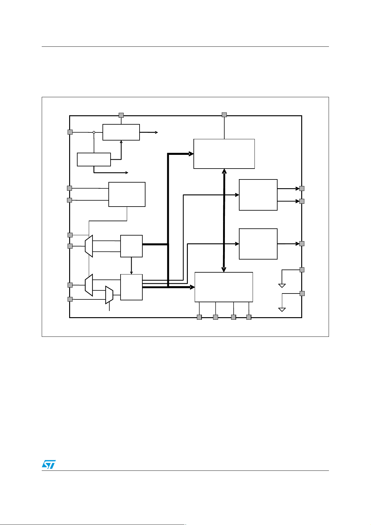
STPMC1 Functional block diagram
1 Functional block diagram
Figure 1. STPMC1 device block diagram
VDD
VCC
VCC
XTAL1
XTAL1
XTAL2
XTAL2
Band Gap
Band Gap
VDD
Linear Vregs
Linear Vregs
VBG
VBG
BIAS
BIAS
Clock
Clock
Generator
Generator
POR
POR
CONFIGURATORS
CONFIGURATORS
VOTP
VOTP
112 OTP
112 OTP
STEPPER
STEPPER
DRIVER
DRIVER
MOP
MOP
MON
MON
CLK
CLK
DAx
DAx
DAN
DAN
DAH
DAH
0
0
1
1
0
0
1
1
DAx-C
DAx-C
DAx-V
DAx-V
DAN-C
DAN-C
DAN-V
DAN-V
ENH
ENH
xDSP
xDSP
NDSP
NDSP
SPI Interface
SPI Interface
SCS SYN
SCL
SCS SYN
SCL
Energy to Freq
Energy to Freq
Converters
Converters
SDA
SDA
Note: DAx stands for DAR, DAS, DAT, and xDSP stands for RDSP, SDSP, TDSP.
LED
LED
VSSA
VSSA
VSS
VSS
Doc ID 15728 Rev 6 7/77
Page 8

Pin configuration STPMC1
2 Pin configuration
Figure 2. Pin connections (top view)
MON
MON
MOP
MOP
SCS
SCS
V
V
DD
DD
V
V
SS
SS
V
V
CC
CC
V
V
OTP
OTP
DAH
DAH
DAR
DAR
DAS
DAS
STPMC1
STPMC1
LED
LED
SDATD
SDATD
SCLNLC
SCLNLC
XTAL1
XTAL1
XTAL2
XTAL2
SYN
SYN
V
V
SSA
SSA
CLK
CLK
DAN
DAN
DAT
DAT
Table 2. Pin description
Pin n° Symbol Type
(1)
Name and function
1 MON D / P O Programmable output pin, see
2 MOP D / P O Programmable output pin, see
3 SCS D I Digital input pin, see
Ta bl e 5
Ta b l e 5
Ta b l e 5
4VDDA O 1.8 V output of internal low drop regulator which supplies the digital core
5V
SS
A GND Ground level for pad-ring and power supply return
6VCCP I Supply voltage
7V
OTP
P I Supply voltage for OTP cells
8 DAH D I Input for non-multiplexed ΔΣ signals
9 DAR D I Input for multiplexed ΔΣ R-phase signals
10 DAS D I Input for multiplexed ΔΣ S-phase signals
11 DAT D I Input for multiplexed ΔΣ T-phase signals
12 DAN D I Input for multiplexed ΔΣ PTAT and neutral signal
13 CLK D O 2 mA clock output for STPMSx devices
14 V
SSA
15 SYN D I/O Programmable input/output pin, see
A GND Ground level of core
Ta bl e 5
16 XTAL2 A Crystal oscillator pin
17 XTAL1 A Crystal oscillator pin
18 SCLNLC D I/O Programmable input/output pin, see
19 SDATD D I/O Programmable input/output pin, see
20 LED D O Programmable output pin, see
1. A: Analog, D: Digital, P: Power, I: Input, O: Output, GND: Ground
8/77 Doc ID 15728 Rev 6
Ta bl e 5
Ta bl e 5
Ta b l e 5
Page 9

STPMC1 Maximum ratings
3 Maximum ratings
Table 3. Absolute maximum ratings
Symbol Parameter Value Unit
DC input voltage - 0.3 to 6 V
Current on any pin (sink/source) ± 150 mA
Input voltage at all pins -0.3 to V
+ 0.3 V
CC
Input voltage at OTP pin - 0.3 to 25 V
V
V
I
V
CC
PIN
ID
OTP
ESD Human body model (all pins) ± 3.5 kV
T
T
T
STG
OP
J
Operating ambient temperature - 40 to 85 °C
Junction temperature - 40 to 150 °C
Storage temperature range - 55 to 150 °C
Note: Absolute maximum ratings are those values beyond which damage to the device may occur.
Functional operation under these condition is not implied.
Table 4. Thermal data
Symbol Parameter Value Unit
R
thJA
1. This value refers to single-layer PCB, JEDEC standard test board.
Thermal resistance junction-ambient 114.5
(1)
°C/W
Doc ID 15728 Rev 6 9/77
Page 10

Functions STPMC1
4 Functions
Table 5. Programmable pin functions
Programmable pin Standalone mode (APL = 2 or 3) Peripheral mode (APL = 0 or 1)
MON Output for stepper node (MB) - charge pump Watchdog reset
MOP Output for stepper node (MA) - charge pump
LED 3-phase energy pulsed output Programmable energy pulsed output
SCLNLC No load indicator
SYN-NP Negative power indicator
SCS SPI data transmission enable
ZCR
SPI interfaceSDATD Tamper indicator
signal
10/77 Doc ID 15728 Rev 6
Page 11

STPMC1 Application
5 Application
Figure 3. Application schematic in standalone operating mode
N R S T
N R S T
Current
Current
Sensor
Sensor
Voltage
Voltage
Sensor
Sensor
Current
Current
Sensor
Sensor
Voltage
Voltage
Sensor
Sensor
Current
Current
Sensor
Sensor
Voltage
Voltage
Sensor
Sensor
STPMS1
STPMS1
STPMS1
STPMS1
STPMS1
STPMS1
3 V to 5.5 V
3 V to 5.5 V
VCC
VCC
DAR
DAR
DAS
DAS
DAT
DAT
DAN
DAN
DAH
DAH
CLK XTAL1 XTAL2
CLK XTAL1 XTAL2
Stepper
Stepper
Counter
Counter
MOPMONVOTP
MOPMONVOTP
STPMC1
STPMC1
VSS
VSS
LED
LED
SCS
SCS
SYN-NP
SYN-NP
SCL-NC
SCL-NC
SDA-TD
SDA-TD
VDD
VDD
VSSA
VSSA
Pulsed output
Pulsed output
Negative power
Negative power
No load condition
No load condition
Tamper Detection
Tamper Detection
Current
Current
Sensor
Sensor
Figure 4. Application schematic using an MCU
N R S T
N R S T
Current
Current
Sensor
Sensor
Voltage
Voltage
Sensor
Sensor
Current
Current
Sensor
Sensor
Voltage
Voltage
Sensor
Sensor
Current
Current
Sensor
Sensor
Voltage
Voltage
Sensor
Sensor
STPMS1
STPMS1
STPMS1
STPMS1
STPMS1
STPMS1
STPMS1
STPMS1
3 V to 5.5 V
3 V to 5.5 V
Zero
Zero
Crossing
Crossing
DAR
DAR
DAS
DAS
STPMC1
DAT
DAT
DAN
DAN
DAH
DAH
STPMC1
CLK XTAL1 XTAL 2
CLK XTAL1 XTAL 2
MOPMONVOTPVCC
MOPMONVOTPVCC
VSS
VSS
Watchdog
Watchdog
LED
LED
SCS
SCS
SYN-NP
SYN-NP
SCL-NC
SCL-NC
SDA-TD
SDA-TD
VDD
VDD
VSSA
VSSA
Pulsed
Pulsed
Output
Output
Energy
Energy
To MCU
To MCU
Current
Current
Sensor
Sensor
TEMP
TEMP
Sensor
Sensor
STPMS1
STPMS1
Doc ID 15728 Rev 6 11/77
Page 12

Application STPMC1
Table 6. Typical external components
Function Component Value Tolerance Unit
Reads or writes to a calculator device via SPI and
performs computation
Measurement reference clock Crystal oscillator
Interface R-phase voltage, current STPMSx --- --- ---
Interface S-phase voltage, current STPMSx --- --- ---
Interface T-phase voltage, current STPMSx --- --- ---
Interface PTAT, neutral current STPMSx --- --- ---
Interface PTAT or hall STPMSx --- --- ---
Low-end user interface Stepper counter
Microprocessor --- --- ---
4.194
8.192
4.915
9.830
± 30 ppm MHz
Note: The components listed above refer to a typical metering application. In any case, STPMC1
operation is not limited to the choice of these external components.
12/77 Doc ID 15728 Rev 6
Page 13

STPMC1 Electrical characteristics
6 Electrical characteristics
(VCC = 5 V, TA= - 40 to + 85 °C, 100 nF across VCC and VSS; 1 µF across VDD and V
SSA
unless otherwise specified).
Table 7. Electrical characteristics
Symbol Parameter Test conditions Min. Typ. Max. Unit
Energy measurement accuracy
f
BW
General Section
V
CC
I
CC
ΔI
CC
POR Power on reset on V
V
DD
V
OTP
I
OTP
Effective bandwidth Limited by digital filtering
5400Hz
Operating supply voltage 3.17 5.5 V
Supply current. Configuration
registers cleared or device
locked
f
=4.194MHz;
XTAL1
V
=3.2V; CL=100nF; no
CC
loads
567mA
Increase of supply current per
configuration bit, during
f
=4.194MHz; VCC=3.2V 100 µA/bit
XTAL1
programming
f
CC
=4.194MHz 2.5 V
XTAL1
Digital supply voltage 1.70 1.80 1.90 V
OTP programming voltage 14 20 V
OTP programming current per
bit
Single bit programming 5 mA
,
t
OTP
I
LATCH
OTP programming time per bit Single bit programming 500 µs
Current injection latch-up
immunity
Digital I/O (DAH, DAR, DAS, DAT, DAN, CLK, SDA, SCS, SYN, LED)
V
V
V
V
I
t
Input high voltage Other pins 0.75V
IH
Input low voltage Other pins 0.25V
IL
Output high voltage IO=-2mA VCC-0.4 V
OH
Output low voltage IO=+2mA 0.4 V
OL
Pull up current 15 µA
UP
Transition time C
TR
LOAD
=50pF, V
=5V 10 ns
CC
Power I/O (MOP, MON)
V
V
t
Output high voltage IO=-16mA 0.9V
OH
Output low voltage IO=+16mA 0.1V
OL
Transition time C
TR
LOAD
=50pF, V
=5V 10 ns
CC
CC
CC
300 mA
V
V
CC
V
V
CC
Doc ID 15728 Rev 6 13/77
Page 14

Electrical characteristics STPMC1
Table 7. Electrical characteristics (continued)
Symbol Parameter Test conditions Min. Typ. Max. Unit
Crystal oscillator
V
V
I
R
C
f
XTAL1
f
MCLK
f
CLK
Input high voltage 1.2 V
IH
Input low voltage 0.6 V
IL
Input current on XTAL2 V
in
External resistor 1 4 MΩ
p
External capacitors 22 pF
p
Nominal output frequency
Internal clock frequency see
Output CLK pin frequency
SPI interface timing
F
SCLKr
F
SCLKw
t
t
t
t
OFF
t
SYN
DH
ON
Data read speed TA= 25°C 32 MHz
Data write speed TA= 25°C 100 kHz
Data setup time 20 ns
DS
Data hold time 0 ns
Data driver on time 20 ns
Data driver off time 20 ns
SYN active width 2/f
=5.3V -1 +1 µA
CC
4.000 4.194 4.915
8.000 8.192 9.830
Ta bl e 1 0
HSA
= 0 f
= 1 f
HSA
8.000 8.192 9.830 MHz
/4
XTAL1
/2
XTAL1
XTAL1
MHz
MHz
s
Note: Typical value, not production tested.
14/77 Doc ID 15728 Rev 6
Page 15

STPMC1 Terminology
7 Terminology
7.1 Measurement error
The error associated with the energy measured by the STPMC1 is defined as:
EnergyTrue)reading(1SPMC
−
EnergyTrue
7.2 Conventions
The lowest analog and digital power supply voltage is called VSS which represents the
system ground (GND). All voltage specifications for digital input/output pins are referred to
GND.
Positive currents flow into a pin. “Sinking current” is the current flowing into the pin, and so it
is positive. “Sourcing current” is the current flowing out of the pin, and so it is negative.
Signal timing specifications treated by a digital control part are relative to XTAL1. This signal
is provided from the crystal oscillator or from an external source as specified in paragraph
9.4
.
ErrorPercentage
=
Signal timing specifications of the SPI interface are relative to the SCLNLC. There is no
direct relationship between the clock (SCLNLC) of the SPI interface and the clock of the
DSP block (XTAL1).
A positive logic convention is used in all equations.
Doc ID 15728 Rev 6 15/77
Page 16

Terminology STPMC1
7.3 Notation
Table 8. Notation
Label Description
uVoltage
i Current
u
X
i
X
i
N
U
X
I
X
P Active energy full bandwidth
F Active energy fundamental
Q Reactive energy full bandwidth
R Reactive energy fundamental
X
Y
PIN Pin names are UPPERCASE
CFG
Phase X voltage (X = R, S, T)
Phase X current (X = R, S, T)
Neutral current
Phase X RMS voltage (X = R, S, T)
Phase X RMS current (X = R, S, T)
X energy type per Y phase
X = P, F, Q, R
Y = R, S, T or Σ for 3-phase
Configuration bit names are UNDERLINED
SIG
Internal signals and status bits are in
ITALICS
16/77 Doc ID 15728 Rev 6
Page 17

STPMC1 Typical performance characteristics
8 Typical performance characteristics
Figure 5. Supply current vs. supply voltage, TA = 25°C (f
8
8
7,5
7,5
7
7
6,5
6,5
6
6
(mA)
(mA)
CC
CC
I
I
5,5
5,5
5
5
4,5
4,5
4
4
3 3,5 4 4,5 5 5,5 6
3 3,5 4 4,5 5 5,5 6
V
V
CC
CC
(V)
(V)
XTAL1
Figure 6. Digital voltage regulator: line - load regulation. (f
1 µF across V
2,5
2,5
DD
and V
; TA = 25 °C)
SSA
= 4.194 MHz, f
ICC25°C
ICC25°C
ICC-40°C
ICC-40°C
ICC85°C
ICC85°C
= 0; 100 nF across VCC and VSS;
XTAL1
= 8.192 MHz)
XTAL1
2
2
1,5
1,5
(V)
(V)
1
1
DD
DD
V
V
0,5
0,5
0
0
0123456
0123456
-0,5
-0,5
V
V
(V)
(V)
CC
CC
Doc ID 15728 Rev 6 17/77
Page 18

Typical performance characteristics STPMC1
Figure 7. Gain response of decimator
Flat band (10Hz Flat band (10Hz – 300Hz)
Flat band (10Hz Flat band (10Hz – 300Hz)
3 dB band (4Hz 3 dB band (4Hz –700Hz)
3 dB band (4Hz 3 dB band (4Hz –700Hz)
18/77 Doc ID 15728 Rev 6
Page 19

STPMC1 Theory of operation
9 Theory of operation
9.1 General operation
The STPMC1 (also called a calculator) is an ASSP designed for effective measurement in
power line systems utilizing the Rogowski coil, current transformer, Shunt or Hall current
sensors. This device, used with the STMicroelectronics STPMSx companion chip (an
analog front-end device), can be implemented as standalone or as a peripheral in a
microprocessor based 1-, 2- or 3-phase energy meter.
The calculator consists of three sections: analog, digital and OTP (see
● The analog section is composed of a band-gap voltage reference and a low-drop
voltage regulator.
● The digital section consists of a system control, clock generator, three PDSP and a
NDSP, a SPI interface.
● The 112-bit OTP block and the 16 system signals, used for testing, configuration and
calibration purposes, are controlled through SPI by means of a dedicated command
set.
The calculator has five input data pins, of which four are fed by signals generated by the
STPMSx, see
Ta b le 9
.
Three of them (DAR/DAS/DAT) are used to receive multiplexed signals of voltage and
current, implementing energy measurement in 1-, 2- and 3-phase (3 and 4 wires) systems.
After being de-multiplexed, each phase input is sent to the correspondent DSP unit that
processes voltage and current information and performs energy calculation, according to
the settings of the configuration bits (see
The DAN input, which also receives a multiplexed signal output from STPMSx device, is
typically used to monitor neutral current for anti tampering functions in 1-, 2- and 3-phase (4
wires) systems. Normally the STPMSx monitors current and voltage but in case of neutral
monitoring the voltage channel can be connected to a different type of sensor, for example a
temperature sensor.
The fifth input data pin (DAH) accepts non-multiplexed ΔΣ signals. It can be used for EMI
sensing through Hall sensors or for temperature sensing.
Table 9. Input channels from the STPMSx
Ta bl e 33
Figure 1
):
).
Channel name Property Signal 1 Signal 2
DAR Multiplexed Voltage Current
DAS Multiplexed Voltage Current
DAT Multiplexed Voltage Current
DAN Multiplexed Temperature Current
DAH Not multiplexed EMI or temperature
The companion chip (STPMSx) embeds 2 ΔΣ ADC converters and the necessary logic
capable of providing the multiplexed ΔΣ streams.
See the STPMSx documentation for more details.
Doc ID 15728 Rev 6 19/77
Page 20

Theory of operation STPMC1
These four multiplexed signals are separated, by a digital de-multiplexer, back into eight ΔΣ
signals, called streams. The signal coming from the voltage channel of the STPMSx is
named with the suffix V, while the stream coming from the current channel is named with the
suffix C. For example, the voltage stream of the S-phase is named DAS-V.
Then, each pair of phase the voltage and current stream coming from DAR, DAS and DAT is
connected to a dual-channel RDSP, SDSP, TDSP unit (i.e. DAR-V and DAR-C are
connected to RDSP).
Each phase voltage input stream is proportional to phase voltage u. Each phase current
input stream is proportional to derivation of phase current di/dt, when it originates from
Rogowski coil, or to phase current i, when it originates from Shunt or CT or Hall sensor. In
this case a derivative is inserted into the voltage channel to get a stream proportional to
du/dt. The sensors differ from each other for sensitivity, phase error and susceptibility to
external EM fields.
Each of these DSP units performs the following:
● checks the integrity of the streams
● calibrates streams
● filters both streams with a dedicated decimation filter
● computes active and reactive energies, momentary and RMS values for voltage and
current, period of power line voltage signal.
In each DSP there are calibrators capable of adjusting the readings ±12.5%.
The power computer does the final calculations of the value and direction of the power and
checks for no-load condition.
Another dual DSP unit, called NDSP, processes the streams coming from DAN and DAH. In
fact, using the ENH
bit (see
Ta bl e 33
), the user can select either the voltage stream of the
DAN pin (DAN-V) or the DAH stream as the input of the NDSP unit, while the current stream
DAN-C is always processed as neutral current.
In its voltage channel, the NDSP unit uses a 2 s time multiplex to process two streams.
During the first half of the interval the voltage input stream is processed (which can be DANV or DAH, according to the ENH
bit), while during the second half a stream constituted by
the sum of all four calibrated currents (i.e. DAR-C + DAS-C + DAT-C + DAN-C).
In its current channel the NDSP unit process the current stream of the neutral conductor as
follows:
● checks the integrity of stream
● calibrates the stream
● filters the stream with a dedicated decimation filter
● computes momentary and RMS values of the stream
● if no errors have been detected in the phase timing, computes phase frequency,
integrates the phase powers by means of 3-input integrators of energies and generates
all pulse output signals.
When the DAH input stream is selected, it is checked to detect an external magnetic
influence (EMI) to the meter.
20/77 Doc ID 15728 Rev 6
Page 21

STPMC1 Theory of operation
The calculator, thanks to its flexibility, can work in all worldwide distribution network
standards. By programming the SYS
OTP bits, it is possible to implement the following
systems:
● 3-phase, 4-wire RSTN, 4-system RSTN (tamper);
● 3-phase, 4-wire RSTN, 3-system RST;
● 3-phase, 3-wire RST_, 3-system RST_ (tamper);
● 3-phase, 3-wire RST_, 2-system R_T_ (Aron);
● 2-phase, 3-wire _STN, 2-system _ST_ (America);
● 1-phase, 2-wire __TN, 2-system _ST_ (tamper coil:coil);
● 1-phase, 2-wire __TN, 2-system _ST_ (tamper coil:shunt);
● 1-phase, 2-wire __TN, 1-system __T_.
The results of all DSP units are available as pulse frequency on pin LED, MOP and MON,
which can also drive a stepper counter, and as states on the digital outputs of device or as
data bits in data records, which can be read from the device by means of SPI interface from
pins SDA, SNC, SCL and SYN. This system bus interface is also used during temporary or
permanent programming OTP bits and system signals or to execute a remote reset request.
A logic block common to all DSP units performs other operations like:
● selecting the valid phase period result from which line frequency is computed in NDSP
unit
● checking the equality of phase angles between all three phase voltages
● preparing current values for compensation of external intermediate phase magnetic
influences
● checking the sum of currents
● computing intermediate phase voltages
● combining the 3-phase status bits
● performing a watchdog user function
After the device is fully tested, configured and calibrated, a dedicated bit of the OTP block,
called TSTD, can be written permanently in order to prevent the change of any configuration
bit.
9.2 Power supply
The supply pins for the analog part are VCC and VSS. The VCC is the power input of the 1.8
V low drop regulator, band-gap reference and bias generators.
From the V
used to power the OTP module and digital core. The V
for all the internal signals. 100 nF low ESR capacitors should be connected between V
and V
SS
to the device.
The STPMC1 contains a power on reset (POR) detection circuit. If the V
than 2.5 V then the STPMC1 goes into an inactive state, all the functions are blocked
asserting a reset condition. This is useful to ensure correct device operation at power-up
and during power-down. The power supply monitor has built-in hysteresis and filtering,
which gives a high degree of immunity from false triggering due to noisy supplies.
A bandgap voltage reference (VBG) of 1.23 V ±1% is used as a reference voltage level
pin a linear regulator generates the +1.8 V voltage supply level (VDD) which is
CC
, and 1 µF between VDD and V
pin represents the reference point
SS
. All these capacitors must be placed very close
SSA
supply is less
CC
Doc ID 15728 Rev 6 21/77
CC
Page 22

Theory of operation STPMC1
source for the linear regulator. Also, this module produces several bias currents and
voltages for all other analog modules and for the OTP module.
9.3 Resetting the STPMC1 (status bit
HLT
The STPMC1 has no reset pin. The device is automatically reset by the power-on-reset
detection circuit (POR) when the V
crosses the 2.5 V value, but it can be reset also
CC
through the SPI interface through a dedicated remote reset request (RRR) command (see
paragraph
9.21
for RRR details).
The reset through SPI is used during production testing or in an application with some onboard microprocessors when a malfunction of the device is detected.
Resetting the STPMC1 causes all the functional modules of STPMC1 to be cleared,
including the OTP shadow latches (see paragraph
9.19
for an OTP shadow latch memory
description). In case of reset through SPI the mode signals (see paragraph
description of the mode signals) are not cleared.
In cases of reset caused by the POR circuit all blocks of the digital part, except the SPI
interface, are held in a reset state for 125 ms after the reset condition. When the reset is
performed through SPI, no delayed turn-on is generated.
During the device reset, the status bit
HLT
is held high, meaning that data read from the
device register are not valid.
9.4 Clock generator (bits MDIV, FR1, HSA)
All the internal timing of the STPMC1 is based on the XTAL1 signal. This signal can be
generated in two different ways:
● Quartz: the oscillator works with an external crystal.
● External clock: the clock is provided by an external source connected to XTAL1.
)
9.20
for a
The suggested circuits are depicted in
Figure 8. Connections of oscillator: (a) quartz, (b) external source
22/77 Doc ID 15728 Rev 6
Figure 8
.
Page 23

STPMC1 Theory of operation
The clock generator is responsible for two tasks.
The first is to retard the turn-on of some functional blocks after POR in order to help a
smooth start of external power supply circuitry by keeping off all major loads. For this
reason, all blocks of the digital part, except the SPI interface, are held in a reset state for 125
ms after a power on reset (see
Section 9.3
).
The second task of the clock generator is to provide all necessary clocks for the digital part.
In this task, a MDIV
nominal frequency value from XTAL1 (f
Four nominal frequencies are possible through proper setting of the MDIV
Ta bl e 10
).
and FR1 programming bits are used to inform the device about the
).
XTAL1
and FR1 bits (see
The internal master clock f
Table 10. Frequency settings through MDIV
f
XTAL1
4.194 MHz 0 0 8.389 MHz
4.915 MHz 0 1 9.830 MHz
8.192 MHz 1 0 8.192 MHz
9.830 MHz 1 1 9.830 MHz
1. 4 MHz and 8 MHz clock are also supported. MDIV and FR1 have to be set as for 4.194 MHz and 8.192
MHz respectively.
Through the HSA bit the frequency of the output pin CLK (f
the STPMSx devices, can be derived as reported in
Table 11. CLK pin frequency settings through HSA
HSA (1 bit) f
0f
1f
To properly work with STPMS2, the clock configurations in
Moreover, with STPMS2 companion chip the PM
Table 12. STPMC1 configuration for STPMS2
is derived from f
MCLK
MDIV (1 bit) FR1 (1 bit) f
as shown in
XTAL1
and FR1
Ta bl e 11
Ta bl e 10
(1)
), which provides the clock for
CLK
.
STPMC1
CLK
/ 4
XTAL1
/ 2
XTAL1
Ta bl e 12
must be used.
bit must always be set.
.
MCLK
MDIV (1 bit) HSA (1 bit) f
00f
10f
01f
9.5 Zero crossing detection (signal
The STPMC1 has a zero crossing detection circuit on the voltage channel that can be used
to synchronize some utility equipment to zero crossing or max of line voltage events. This
circuit produces the internal signal
the line voltages and a rising edge every peak (positive or negative) of one of the line
voltages.
ZCR
that has a falling edge every zero crossing of one of
Doc ID 15728 Rev 6 23/77
ZCR
CLK
/ 4
XTAL1
/ 4
XTAL1
/ 2
XTAL1
)
Page 24

Theory of operation STPMC1
The
ZCR
Figure 9.
signal is a 3-phase voltage zero cross signal. It is the result of a XNOR of the
of each phase. The
is 300 Hz signal. The
ZCR
of each of the three-phases is a 100 Hz signal, so a 3-phase
ZCR
signal is available on the MOP pin only when the STPMC1 works
as a peripheral with the configuration bit APL
ZCR
signal
=0.
ZCR
ZCR
9.6 Period and line voltage measurement (status bits:
LOW, BFF
From voltage channels, a base frequency signal
voltage is rising and it is low when the line voltage is falling, so that,
the sign of dv/dt. With further elaboration, the
A period meter, which is counting up pulses of f
period of voltage channel base frequency and checks if the voltage signal frequency is in the
band going from f
This is done, phase by phase, by means of the signal
and it is used to reset the period meter.
Table 13. Good frequency ranges for different clock source values
4.194 MHz 8.389 MHz 32.0 Hz 128.0 Hz
4.915 MHz 9.830 MHz 37.5 Hz 150.0 Hz
8.192 MHz 8.192 MHz 31.3 Hz 125.0 Hz
9.830 MHz 9.830 MHz 37.5 Hz 150.0 Hz
f
XTAL
If the counted number of f
18
2
equivalent pulses or if the counting is never stopped (no more
base frequency exceeds the lower limit and an error flag
the 8-bit status byte of each phase (see
)
f
MCLK
MCLK
/(2
LIN
is obtained, which is high when the line
ZCR
signal is also produced.
/8 reference signal, measures the
MCLK
18
- 23) ≈ f
freq. min. = f
/8 pulses between two trailing edges of
MCLK
MCLK
/218 to f
MCLK
/216.
MCLK
LIN
, which trailing edge is extracted
/218 freq. max. = f
BFR
Ta bl e 32
).
LIN
signal represents
LIN
is higher than the
LIN
trailing edge), the
is set. This error flag is part of
LIN, BFR
16
/2
MCLK
,
24/77 Doc ID 15728 Rev 6
Page 25

STPMC1 Theory of operation
Figure 10.
If the counted number of f
16
2
equivalent pulses, the base frequency exceeds the upper limit. In this case, such error
must be repeated three times, in order to set the error flag
LIN
and
BFR
behavior when f
/8 pulses between two trailing edges of
MCLK
line
> f
MCLK
/2
16
BFR
, as shown in
LIN
is lower than the
Figure 10
.
The in-band base frequency resets the flag
BFR
. If
BFR
is cleared, the measured period
value is latched, otherwise a default value of period is used as a stable data to compute
frequency needed to adapt the decimation filter and to perform frequency compensation of
reactive energy and RMS current I
The
BFR
flag is also set if the register value of the RMS is too low. In this case also the
status bit
The condition for setting
(U
Xmax
LOW
is set.
LOW
= 212) it means if the UX register drops below 128
the register value goes above 256 (U
in case of non Rogowski current sensor.
X
and consequently
BFR
of each phase is UX < U
LOW
X
> U
Xmax
/16).
BFR
, then, gives also information about
and
BFR
the presence of the line voltage.
When the
BFR
error is set, the computation of power is zero and the energy registers
(active, reactive and fundamental) are blocked, unless single wire mode operation is entered
(see
Section 9.7
).
When the MOP, MON and LED pins are configured to provide the pulsed energy information
they are held low if
The 3-ph status bit
BFR
is set.
BFF
is the OR of each phase bit
BFR
.
9.7 Single wire operation mode: SWM (status bits:
configuration bit FRS
The STPMC1 supports single wire meter (SWM) operation. In this condition, since there is
no voltage information, the current RMS values, instead of the energies, are accumulated in
20-bit dedicated registers located in ACR, ACS, ACT (20-bit accumulator of RMS I
[Ah]).
)
/32
Xmax
are cleared when
NAH, BFR
per hour
X
,
Doc ID 15728 Rev 6 25/77
Page 26

Theory of operation STPMC1
Each ACx register contains a 20-bit accumulator of the relative phase current IX [Ah] and an
8-bit register carrying the information about phase delay between voltage channels.
The SWM mode is indicated by status bit
● Bit
NAH
I
/4096 = 16 (I
Xmax
=0 (SWM on) happens when
= 216). In this case frequency is out of limits and RMS current IX
Xmax
NAH
=0:
BFR
=1 and RMS value of current signal is IX >
is big enough, so it is accumulated in the corresponding ACx phase register.
● Bit
When bit
are blocked. Then, if RMS value of current signal is big enough, bit
NAH
I
/8192 = 8, or
Xmax
current I
BFR
=1 (SWM off) happens if
BFR
=0. In this case either voltage frequency is out of limits but RMS
is too small to enter SWM mode, or voltage frequency is in the correct range.
X
BFR
=1 and RMS value of current signal is IX <
is set, for a certain phase, its energy registers (active, reactive, fundamental)
NAH
is cleared (0) and a
SWM operation is entered. In this case the RMS value of current signal is accumulated in
ACx register and the value of voltage RMS U
is set to zero.
X
Example 1: Single wire operation with SYS = 0
SYS = 0 (3-phase system) is set and in the R-phase the voltage signal is too low
(status bits of phase R
BFR
= 1 and
LOW
= 1).
Because of the too low voltage signal the frequency can't be calculated and energy
registers related to the R-phase are blocked.
If RMS value of current signal is big enough, the device enters SWM and clears
R phase. The ACR register is incremented by adding I
, the RMS value of current
R
NAH
signal.
Example 2: Single wire operation with SYS = 0 and TCS = 1
of
SYS = 0 (3-phase system) and TCS = 1 (CT sensor selection) are set and in all phases
(R, S and T) the voltage signal is too low (status bits
phases).
Because of the too low voltage signal the frequency could not be calculated and all
energy registers are blocked.
Since when TCS
= 1, a frequency value is needed to calculate the RMS value of the
current signal, the default value of 50 Hz or 60 Hz (if bit FRS
value of current signal is big enough, the device enters SWM and clears
phases and ACR, ACS and ACT registers is fed with the correspondent I
The accumulators ACx can be read by means of SPI.
To retrieve energy information, RMS value of current signal accumulated in registers ACx
can be multiplied by a constant representing the value of RMS voltage. This operation must
be executed by a microcontroller.
Usually the supply voltage for the electronic meter is taken from the line voltage. In SWM,
since the line voltage is not present anymore, some other power source must be used in
order to provide the necessary supply to STPMC1 and the other electronic components of
the meter.
9.8 Load monitoring (status bit
The STPMC1 includes in each phase a no-load condition detection circuit with adjustable
threshold. This circuit monitors the voltage and the current channels and, when the
measured voltage is below the set threshold, an internal signal
BFR
= 1 and
LOW
=1) is taken. If the RMS
BIL
, configuration bit LTCH)
BIL
becomes high. The
= 1 for all
NAH
of all
.
X
26/77 Doc ID 15728 Rev 6
Page 27

STPMC1 Theory of operation
information about this signal is also available in the status bit
Ta bl e 32
The three phase status bit
The no-load condition occurs when the product between U
a given value. This value can be set by the LTCH
threshold values can be chosen according to the two LTCH
When a no-load condition occurs (
load condition flag
brought out to the output selector forcing SCLNLC pin low. In peripheral mode, the
signal can be accessed through the SPI interface.
The minimum output frequency (at no-load threshold) is given as % of the full-scale (FS)
output frequency, where FS internal AW frequency is 1370 Hz per phase.
Table 14. No-load detection thresholds
LTCH (2 bits) NLC threshold
).
BIL
BIL
in standalone mode blocks generation of pulses for stepper and is
0 0,00125*FS
1 0,0025*FS
2 0,005*FS
3 0,010*FS
BIL
, one per each phase (see
is the AND of each phase status bit
and IX register values is below
configuration bits. Four different no-load
BIL
= 1) the integration of power is suspended. The no-
X
bits as reported in
BIL
.
Ta bl e 14
BIL
.
Example 3: No-load condition threshold calculation
An energy meter has a power constant of C = 64000 pulses/kWh on LED pin.
It is valid the following relation:
C = 3600000 * f / P
where 3600000 is the factor between kWh and Ws and f is the output frequency on the
LED pin if P power is applied to the meter.
The minimum output frequency if LTCH
f = 0,010 * 1370 Hz = 0,137 Hz
which gives a no-load condition power threshold equal to:
P = 3600000 * 0,137 Hz / 64000imp/kWh = 7,7 W
In this example, the no-load threshold is equivalent to 7,7 W of load or to a start-up
current of 32 mA at 240 V.
In NLC function is also implemented an hysteresis. When the current is falling the threshold
is half lower than that described above.
9.9 Error detection (status bits:
The STPMC1 has two error detection circuits that checks:
● the ΔΣ signals
● the state of output pins
[0] = LTCH [1] = 1 is:
BCF, PIN
)
The first error detection circuit checks if any of the ΔΣ signals from the analog part is stuck at
1 or 0 within the period of observation (250 µs). In case of detected error the corresponding
ΔΣ signal is replaced with an idle ΔΣ signal, which represents a constant value 0. When this
Doc ID 15728 Rev 6 27/77
Page 28

Theory of operation STPMC1
error occurs the correspondent phase bit
again the
The 3-ph status bit
connection of the neutral wire (DAN-I stream).
The other error condition occurs if the MOP, MON and LED pin outputs signals are different
from the internal signals that drive them. This can occur if some of this pin is forced to GND
or to some other imposed voltage value. In this case the internal status bit
immediately activated providing the information that some hardware problem has been
detected, for example the stepper motor has been mechanically blocked.
These two error condition don't influence energy accumulation.
BCF
flag is cleared immediately.
BCF
is the OR of each phase bit BFC, but it takes into account also the
BCF
is set. When the ΔΣ signal becomes correct
9.10 Tamper detection module (status bits:
configuration bit ENH
The tamper detection module is used to prevent theft of energy through improper connection
of the meter. The tamper indicator is activated when:
● sum of currents is above tamper threshold (status bit
● phase sequence is wrong (status bit
● phase active powers don't have the same sign (status bit
● electromagnetic interference (EMI) is detected (only with ENH = 1).
)
BSF
= 1),
PIN
BCS, BSF, BIF
BCS
= 1),
BIF
= 1),
is
,
In standalone application mode (APL
condition.
In 3-phase system (SYS
BCS, BSF, BIF
In other systems (SYS
has been set or if EMI has been detected.
= 0, 1, 2) this output is set if at least one of the internal status bits:
≠ 0, 1, 2) it indicates only
[1] = 1) the SDATD pin is used to notify the tamper
BCS
or EMI.
Example 4: Tamper output on SDATD pin
SYS = 0, 1 or 2 and APL [1] = 1:
BCS
= 0,
BSF
= 0,
BIF
= 0 → Tamper (SDATD pin) = 0
BCS
= 0,
BSF
= 1,
BIF
= 1 → Tamper (SDATD pin) = 1
SYS
= 0, 1 or 2, APL [1] = 1 and ENH = 1:
BCS
= 0,
BSF
= 0,
BIF
= 0, EMI = 0 → Tamper (SDATD pin) = 0
BCS
= 0,
BSF
= 0,
BIF
= 0, EMI = 1 → Tamper (SDATD pin) = 1
BCS
= 1,
BSF
= 1,
BIF
= 1, EMI = 1 → Tamper (SDATD pin) = 1
In peripheral application mode these information can be read out by SPI interface checking
the 3-ph status bits, or the status bits corresponding to each phase.
9.10.1 Sum of currents is above tamper threshold (status bit
Tamper detection through bit
neutral wire). In other measurement systems it is not useful because there are not enough
input current streams.
BCS
is meaningful only for SYS = 0, 2, 5, 6 (systems with
BCS
)
The STPMC1 check tamper detection only if
28/77 Doc ID 15728 Rev 6
Page 29

STPMC1 Theory of operation
I
max
I
>
X
∑
256
Where:
= 2
16
I
max
Σ IX = IR + IS + IT + IN for SYS = 0, 1, 2, 3, 4, 7
Σ I
= IS + IT for SYS = 5, 6
X
Bit
BCS
is set according to
Ta bl e 1 5
Table 15. Tamper conditions
BCS
0
1
SYS = 0, 1, 2, 3, 4, 7 SYS = 5, 6
I
X
RMS
RMS
∑
<
8
I
X
∑
>
8
RMS
()
i
∑
X
()
i
∑
X
with (Σ iX)
= (iR + iS + iT + iN)
RMS
7
9
7
9
9
I
II
<<
STS
7
9
I
II
>>
STS
7
or
or
or
7
9
7
9
Example 5: 3-ph system - BCS = 0
Let us consider a three-phase, four wires system where the RMS values of the current
applied are:
I
= 5 A
R
I
= 5 A
S
I
= 4.4 A
T
I
= 0 A
N
The sum of all instantaneous currents (i
there is a tamper condition.
The STPMC1 calculates this sum and put its RMS value divided by four (called sIRMS)
into register DMN (see paragraph
This value should always be zero (or very close).
In our case:
9.17.2
+ iS + iT + iN) should always be zero, unless
R
).
9
I
II
<<
TST
7
9
I
II
>>
TST
7
sIRMS
The currents are shown in
i
∑
below.
⎞
X
4
⎟
⎠
RMS
=
A149967.0
⎛
=
⎜
⎝
Figure 11
Doc ID 15728 Rev 6 29/77
Page 30

Theory of operation STPMC1
()
Figure 11. Currents of the three phase system in example
The value I
register (internal value FFFF). It is a function of the sensor type, sensitivity and of the
current channel gain. Let us suppose that
I
= 180 A
MAX
The tamper condition is evaluated only if
This means that the sum of the RMS value of currents is not negligible with respect to
I
(the threshold corresponds to about 0.4% of I
MAX
In this case this is true since:
I
+ IS +IT +IN = 14.4 A > 0,703125 A = I
R
The criterion for tamper detection is
This can also be expressed as
corresponds to the maximum current value hold by each RMS current
MAX
I
MAX
>+++=
IIIII
MAX
/ 256
∑
>
∑
NTSRX
256
).
MAX
I
X
8
i
X
RMS
4
I
X
∑
>=
32
sIRMS
∑
()
i
X
∑
RMS
i
⎞
⎛
X
=
⎜
⎝
∑
⎟
4
⎠
RMS
which means the sIRMS value must not exceed 3.13% of (I
In this example:
sIRMS = 0,149967 < 0.45 = (I
Then BCS = 0.
30/77 Doc ID 15728 Rev 6
+ IS +IT +IN) / 32
R
+ IS +IT +IN).
R
Page 31

STPMC1 Theory of operation
Example 6: 3-ph system - BCS = 1
Let us consider a three-phase, four wires system where:
I
= 5 A
R
I
= 5 A
S
I
= 3.2 A
T
I
= 0 A
N
The tamper is evaluated because
I
+ IS +IT +IN = 13.2 A > 0,703125 A = I
R
MAX
/ 256
In this case
sIRMS = 0,449901 A > 0,4125 A = (I
+ IS +IT +IN) / 32
R
Then BCS = 1.
Example 7: 1-ph system - BCS = 0
Let us consider a single phase systems with only S and T wires connected where
I
= 5 A
S
I
= 4 A
T
I
= 180 A
MAX
In this case the criterion for tamper evaluation is verified since:
(I
+ IT) = 9 A > 0,703125 A = I
S
But BCS = 0 because
7/9 I
= 3.11 A < IS = 5 A < 9/7 IT = 5.14 A
T
and
7/9 I
= 3.88 A < IT = 4 A < 9/7 IS = 6.43 A
S
MAX
/ 256
Example 8: 1-ph system - BCS = 1
Let us consider the case in which:
I
= 5 A
S
I
= 3 A
T
I
= 180 A
MAX
Also in this case the criterion for tamper evaluation is verified:
(I
+ IT) = 8 A > 0,703125 A = I
S
MAX
/ 256
Now BCS = 1 because
7/9 I
= 3.88 A > IT = 3 A
S
9.10.2 Phase sequence is wrong (status bit
One tamper condition is that phase sequence is not correct. A 3-ph phase status bit
checks the sequence of phases, which, in a three phase system is one of the following:
● R → S → T
● S → T → R
● T → R → S
In one of the above cases
BSF
is cleared, otherwise bit
BSF
)
BSF
BSF
is set.
Doc ID 15728 Rev 6 31/77
Page 32

Theory of operation STPMC1
Whatever the SYS bits setting (indicating phases presence and configuration), bit
always calculated, but it is valid only in cases SYS
three phase voltage signals (u
In cases SYS
is 4, 5, 6, 7, only two or one voltage signal are available (uS and/or uT), so that
the sequence cannot be checked. Bit
, uS, uT) are available and can be checked, as shown in 0.
R
BSF
is always set in the status byte, but it must be
is 0, 1, 2 and 3. In fact in this case all the
BSF
is
ignored.
In standalone application for SYS
= 0, 1 or 2 (3-phase systems) bit
BSF
is available as
output on SDATD pin.
Table 16. Pin description versus SYS configuration (uX and iX represent the voltage and the
current signals)
SYS
Pin01234567
DAR u
DAS u
DAT u
DAN i
DAR i
DAS i
DAT i
R
S
T
N
R
S
T
u
R
u
S
u
T
-------
i
R
i
S
i
T
u
R
u
S
u
T
i
R
i
S
i
T
u
R
u
S
u
T
i
R
-iSi
i
T
----
u
S
u
T
----
i
T
---
u
T
S
i
T
u
T
i
S
i
T
u
T
-
i
T
9.10.3 Phase active powers do not have the same sign (status bit
The 3-phase status bit
equal in all three phases (R, S and T), then bit
In a standalone application for SYS
output on SDATD pin.
Example 9: status bit
SIGN
SIGN
SIGN
SIGN
= 0,
R
= 1,
R
= 1,
R
= 0,
R
SIGN
SIGN
SIGN
SIGN
BIF
is produced from status bit
= 0, 1 or 2 (3-phase system) bit
BIF
= 0,
SIGN
S
= 1,
S
= 0,
S
= 1,
S
SIGN
SIGN
SIGN
= 0 →
T
= 1 →
T
= 0 →
T
= 0 →
T
BIF
BIF
BIF
BIF
BIF
= 0
= 0
= 1
= 1
SIGN
is set.
of each phase. If bit
BIF
is available as
9.10.4 EMI is detected
EMI tamper detection is enabled by configuring bits ENH = 1 and APL [1] = 1 (APL [1] sets
standalone application mode).
The DAH signal is checked to verify that:
● its DC component does not exceed DC
● its RMS value does not exceed the maximum value RMS
where DC
MAX
= RMS
= 216 with hysteresis.
MAX
If these condition are not verified the EMI tamper is detected.
MAX
/16
MAX
/16
BIF
)
SIGN
is not
32/77 Doc ID 15728 Rev 6
Page 33

STPMC1 Theory of operation
EMI tamper condition is not available as internal status signal, but it is available (in OR with
other tamper conditions) on the SDATD pin of the device.
In peripheral application mode it is possible to detect EMI tamper comparing the value of the
16-bit DCuN and of the 12-bit RMSuN to the threshold through a microcontroller.
9.11 Energy to frequency conversion (configuration bits: APL,
KMOT
The STPMC1 provides energy to frequency conversion both for calibration and energy
readout purposes.
The three hard-wired xDSP, implemented as four 2-channel ΔΣ signal processors perform all
calculations and produce output data and signals. Inside them, each three stage decimation
filter inputs a filtered ΔΣ signal and its integral as parallel bus or stream to the power and
RMS computer. All three streams of power (active, reactive and active from the fundamental
harmonic) are connected to the corresponding integrators.
Within the integrators, all three powers are accumulated into energies of 20-bit values
according to configuration bit ABS
frequency of which is proportional to the accumulated energies. Each of these signals can
be brought out to the LED pin.
, LVS, FUND)
and the results are converted into pulse train signals, the
Due to the innovative and proprietary power calculation algorithm the frequency signal is not
affected by any ripple at twice the line frequency. This feature strongly reduces the
calibration time of the meter.
Through calibration the meter is configured to provide a certain number of pulses per kWh
(referred to as power meter constant C) on the LED pin. According to the APL
and FUND
as shown in paragraphs
configuration bits, the frequency of LED signal can provide different information,
9.12
Given C, the number of pulses per kWh provided, the relationship between the LSB value of
the source energy registers and the number of pulses provided to LED pin is indicated in the
table below:
Table 17. Energy registers LSB value
Register SYS = 0, 1, 2, 4, 5, 6, 7 SYS = 3
3-ph active energy wide band (P)
3-ph reactive energy wide band (Q)
3-ph active energy fundamental (F)
and
9.13
.
1000
------------- ----
K
P
⋅
C2
1000
-----------------
K
Q
⋅
C2
1000
------------ -----
K
F
⋅
C2
, KMOT, LVS
1000
------------- ----
Wh[]=
10
Varh[]=
10
Wh[]=
10
K
P
C2
1000
------------- --
K
Q
C29⋅
------------- --
K
F
C2
⋅
1000
⋅
Wh[]=
10
Varh[]=
Wh[]=
9
3-ph reactive energy fundamental (R)
1000
------------ -----
K
R
C210⋅
Varh[]=
1000
------------ ---
K
R
⋅
C2
Varh[]=
9
Doc ID 15728 Rev 6 33/77
Page 34

Theory of operation STPMC1
Example 10: energy registers LSB value for SYS = 0, 1, 2, 4, 5, 6, 7
C = 64000 pulses/kWh = 17.7 Hz*kW
K
= KF = 15.258 *10-6 Wh
P
K
= KR = 15.258 *10-6 VArh
Q
This means that the reading of 0x00001 in the active energy register represents 15.258
µWh, while 0xFFFFF represents 16 Wh.
Example 11: Energy registers LSB value for SYS = 3
C = 64000 pulses/kWh = 17.7 Hz*kW
K
= 15.258 *10-6 Wh
P
K
= 30.517 *10-6 Wh
F
K
= KR = 30.517 *10-6 VArh
Q
From 3-phase active energy wide band signal the stepper driving signals
(output from MOP and MON pins) are generated. The frequency of these signals can be
configured as shown in paragraph
9.13
.
MA
and MB
9.12 Using STPMC1 in microcontroller based meter - peripheral
operating mode (configuration bits: APL
, KMOT, LVS, FUND)
The higher flexibility of the STPMC1 allows its use in microcontroller based energy meters.
In this case the STPMC1 must be programmed to work in peripheral mode setting bit APL
[1] = 0. All the SPI pins (SCS, SCLNCL, SDATD, SYN) are used only for communication
purposes, allowing the microcontroller to write and read the internal STPMC1 registers.
The peripheral mode has two further different configuration modes according to the status of
the APL
described below.
APL
In the MOP pin, the
The pin MON provides the WatchDOG signal. The DOG signal generates a 16 ms long
positive pulse every 1.6 seconds. Generation of these pulses can be suspended if data are
read in intervals shorter than 1.6 ms. The DOG signal is actually a watchdog reset signal
that can be used to control an operation of an on-board microcontroller. It is set to high
whenever the V
run.
It is expected that an application microcontroller should access the data in the metering
device on regular basis, at least 1/s (recommended is 32/s). Every latching of results in the
metering device requested from the microcontroller also resets the watchdog. If latching
requests does not follow each other within 1.6 second, an active high pulse on MON is
produced, because device assumes that microcontroller does not operate properly. This
signal can be either control the RESET pin of the microcontroller or it can be tied to some
interrupt pin. The second chance is recommended for a battery backup application which
can enter some sleep mode due to power down condition and should not be reset by
metering device.
configuration bit, which changes the function of MOP, MON and LED pins as
= 0:
ZCR
signal is available (see paragraph
voltage is below 2.5 V, but after VCC goes above 2.5 V this signal starts to
CC
9.5
for details on
ZCR
signal);
The LED pin can be configured through LVS
signals, as shown in the table below.
34/77 Doc ID 15728 Rev 6
, FUND and KMOT to output different energy
Page 35

STPMC1 Theory of operation
Table 18. LED pin configuration for APL
LV S (1 bit) FUND (1 bit) KMOT (2 bits) LED energy output Phase Freq
0
1R
00
2S
3T
0
1R
01
2S
3T
0
1R
10
2S
3T
0
1R
11
2S
= 0
3-ph
Active energy wide band P
3-ph
Active energy fundamental F
3-ph
Reactive energy wide band Q
3-ph
Reactive energy fundamental R
C
(1)
C
C
C
3T
1. C is the number of pulses per kWh set with calibration.
APL = 1:
MOP/MON provides stepper motor driving signals from 3-phase active energy wide band
register with frequency CM related to C (number of pulses on LED pin, see par.
according to
LED pin provides 3-phase energy pulses according to
to KMOT
.
Ta bl e 20
.
Ta bl e 19
with frequency C not related
Table 19. LED pin configuration for APL = 1
LV S (1 bit) FUND (1 bit) LED energy output Phase Freq
0 0 Active energy wide band P
0 1 Active energy fundamental F
1 0 Reactive energy wide band Q
1 1 Reactive energy fundamental R
3-ph C
9.13 Driving a stepper motor - standalone operating mode
(configuration bits: APL
, LVS, KMOT)
9.11
)
When used in standalone mode (APL[1] = 1), the STPMC1 is able to directly drive a stepper
motor.
Doc ID 15728 Rev 6 35/77
Page 36

Theory of operation STPMC1
From signal PΣ (3-ph active energy), stepper motor driving signals MA and MB (see
Figure 12
) are generated by means of internal divider, mono-flop and decoder and brought
to MOP and MON pins.
Figure 12. Stepper driving signals
Hi
Hi
MON
MON
Low
Low
Hi
Hi
MOP
MOP
Low
Low
The numbers of pulses per kWh on MOP and MON outputs (CM) is related to the number of
pulses on LED pin (C, see par.
9.11
) following the table below.
Table 20. Configuration of MOP and MON driving signals with APL = 1, 2, 3
LV S (1 bit) KMOT (2 bits) Pulses Length Freq. CM
0
0
1
The mono-flop limits the length of the pulses according to the LVS
The decoder distributes the pulses to
1 C/128
2C/32
3 C/256
0
1 C/1280
2 C/320
3 C/2560
31.25 ms
156.25 ms
bit value.
MA
and MB alternatively, which means that each of
them has only a half of selected frequency.
When a no-load condition is detected (
BIL
=1) MOP and MON are held low because
integration of power is suspended.
The LED pin provides 3-phase active energy pulses according to the table below:
C/64
C/640
36/77 Doc ID 15728 Rev 6
Page 37

STPMC1 Theory of operation
Table 21. LED pin configuration for APL
APL (2 bits) KMOT (2 bits) LED energy output Phase Freq
2 - Active energy wide band P 3-ph C
0
1C/128
3
2C/32
3C/256
= 2, 3
C/64
Active energy wide band P 3-ph
9.14 Negative power accumulation (configuration bit ABS, status
SIGN
bit
The ABS bits govern energy accumulation in case of negative power; they only affect active
power P and fundamental active power F.
The 3-ph status bit
status bits
Ta bl e 22
Table 22. Accumulation mode for negative power
ABS
(2 bits)
Accumulation mode Power calculation 3-ph
)
SIGN
depends upon 3-ph cumulative power direction while the phase
SIGN
depends upon phase X power direction.
X
shows power calculation modes according to ABS
SIGN MA
-
MB
0 3-phase Ferraris mode P
Absolute accumulation per
1
phase
2 Ferraris mode per phase
3 Signed accumulation P
= PR + PS + P
Σ
= |PR| + |PS| + |PT|PΣ ≥ 0 →
P
Σ
< 0 → PX = 0
if P
X
= PR + PS + P
P
Σ
= PR + PS + PT
Σ
9.15 Phase delay calculation
The STPMC1 allows the calculation of the phase delays between voltages. If the line
frequency f
is 50 Hz, a 120° phase delay corresponds to 6.7 ms.
line
T
T
PΣ < 0 →
P
≥ 0 →
Σ
PΣ ≥ 0 →
< 0 →
P
Σ
P
≥ 0 →
Σ
SIGN
= 0
SIGN
= 1
SIGN
= 1 PΣ ≥ 0 → see
SIGN
= 1 PΣ ≥ 0 → see
SIGN
= 0
SIGN
= 1
< 0 →
P
Σ
P
Σ
P
Σ
PΣ ≥ 0 → see
MA
≥ 0 → see
< 0 → see
and MB low
Figure 12
Figure 12
Figure 12
Figure 12
Figure 12
Doc ID 15728 Rev 6 37/77
Page 38

Theory of operation STPMC1
Figure 13. Phase delay
tRSt
RS
tSTt
ST
tTRt
TR
The ACR, ACS and ACT registers (bits [7:0], see paragraph 9.17.7) holds the information
needed for this calculation.
Let us indicate t
, tST, tTR, the delays between R, S and T phases. It is:
RS
Equation 1
t
+ tST + t
RS
= T = 1 / ƒ
TR
Concatenating ACT[7:0], ACS[7:0], ACR[7:0] bytes, two 12 bits vectors defined as below are
obtained:
ACT[7:0], ACS[7:0], ACR[7:0] = Asr[12, 10:0], Art[12, 10:0]
The delay times are calculated with the following formulas:
Equation 2
[]
12Asr
⎛
[]
⎜
TRSTAsr
⎝
11
()
+−=−=
120:10Asrtttime ⋅
8
⎞
⎟
f
⎠
MCLK
Equation 3
⎛
[]
⎜
STRSArt
⎝
From
Equation 1, Equation 2
and t
38/77 Doc ID 15728 Rev 6
TR
.
and
Equation 3
it is possible to retrieve phase delays tRS, tST
[]
12Art
11
()
120:10Arttttime ⋅
+−=−=
8
⎞
⎟
f
⎠
MCLK
Page 39

STPMC1 Theory of operation
Example 12: Phase delay calculation
f
= 4 MHz; MDIV = 0; FR1 = 0 → f
XTAL1
f
= 50 Hz → T = 20 ms;
LINE
ACR[7:0] = 0101 1010
ACS[7:0] = 0010 0000
ACT[7:0] = 0000 0101
Asr[12] = 0
Asr[10:0] = 000 0101 0010
Art[12] = 0
Art[10:0] = 00001011010
⎛
[]
⎜
Asr
⎝
μ
⇒
s82
ms20
11
()
°+=°⋅
5,1360
= 82
2
= 90
2
12Asr
[]
+−=
⎞
120:10Asrtime
⎟
⎠
8
MCLK
MCLK
⎛
⎜
⎝
= 8 MHz
0
11
()
2
8
⎞
⋅
+−=⋅
1200000101001
⎟
⎠
6
⋅
108
μ+=
s82
12Art
⇒
Art
[]
⎛
[]
⎜
⎝
μ
s90
ms20
11
()
°+=°⋅
6,1360
+−=
⎞
120:10Arttime
⎟
⎠
8
MCLK
Example 13: Phase delay calculation
f
= 4 MHz; MDIV = 0; FR1 = 0 → f
XTAL1
f
= 50 Hz → T = 20 ms;
LINE
ACR[7:0] = 1011 0011
ACS[7:0] = 0011 1111
ACT[7:0] = 0000 0101
Asr[12] = 0
Asr[10:0] = 000 0101 0011
Art[12] = 1
Art[10:0] = 111 1011 0011
⎛
[]
⎜
Asr
⎝
μ
⇒
s83
ms20
11
()
°+=°⋅
5,1360
= 83
2
= 1971
2
12Asr
[]
+−=
⎞
120:10Asrtime
⎟
⎠
8
MCLK
⎛
⎜
⎝
MCLK
⎛
⎜
⎝
= 8 MHz
0
11
()
2
0
11
()
2
8
⎞
⋅
+−=⋅
1200000101101
⎟
⎠
+−=⋅
1210000101001
6
⋅
108
8
⎞
⋅
⎟
⎠
6
⋅
108
μ+=
s90
μ+=
s83
⇒
Art
12Art
[]
⎛
[]
⎜
⎝
μ−
s76
ms20
11
()
°−=°⋅
4,1360
+−=
Doc ID 15728 Rev 6 39/77
120:10Arttime
⎞
⎟
⎠
MCLK
8
⎛
⎜
⎝
2
1
11
()
⎞
⋅
+−=⋅
1211111011001
⎟
⎠
8
6
⋅
108
μ−=
s76
Page 40

Theory of operation STPMC1
9.16 Calibration (configuration bits: PM, TCS, CIX, CVX, CCA,
, CPX)
CCB
9.16.1 Voltage and current channels calibration
The 8-bit calibration values CVX and CIX (where X stands for N, R, S or T) are used as
static data for the channel ΔΣ calibrators, multiplying their streams to the following factor:
K
= (4096 - 1024 + 4CXX)/4096 (± 12.5 %)
X
When configuration bit PM
respectively:
K
= (8192 - 1024 + 4CXX + CxX)/8192 (± 6.25 %)
X
CvX bits are part of the CCA
byte.
9.16.2 Phase compensation
The STPMC1 does not introduce any phase shift between voltage and current channel.
However, the voltage and current signals come from transducers, which could have inherent
phase errors. For example, a phase error of 0.1° to 0.3° is not uncommon for a current
transformer (CT). These phase errors can vary from part to part, and they must be corrected
in order to perform accurate power calculations. The errors associated with phase mismatch
are particularly noticeable at low power factors.
is set, a 2-bit CvX or CiX is appended to each CVX or CIX
configuration byte while CiX are part of CCB configuration
The STPMC1 provides a means of digitally calibrating these small phase errors introducing
some delay. The amount of phase compensation can be set per each phase using the 4 bits
of the phase calibration configurators (CPR
A vector method of phase shift compensation is implemented.
The compensating voltage vector, which is produced from a frequency compensated signal
of integrated voltage vector multiplied by a given compensation constant per each phase
and is almost perpendicular to the input voltage vector, is subtracted from the input voltage
vector at the input of the decimation filter.
Those phase compensators are merged from a common coarse part CPC
phase 4-bit phase error compensator CPX
CPC
[1] = 0: K
CPC
[1] = 1: K
When either PM
factor:
CPC
[1] = 0: K
CPC
[1] = 1: K
CpC bits are part of the CCA
The equation for phase compensation in degree is:
= - (16 CPC[0] + CPX)
PHC
= (16 - CPX)
PHC
or TCS are set, a 2-bit CpC is appended to CPC to produce the following
= - (32 CpC + 16 CPC[0] + CPX)
PHC
= [64 - (32 CpC + 16 CPC[0] + CPX)]
PHC
configuration byte.
, CPS, CPT).
and from each
:
40/77 Doc ID 15728 Rev 6
Page 41

STPMC1 Theory of operation
Equation 4
f360K⋅°
=ϕ
PHCphc
ϕ
is the phase compensation in degree,
phc
K
is the calculated coefficient,
PHC
f
is the frequency of voltage signal,
line
f
is the clock for phase compensation.
phc
The clock for phase compensation f
Table 2 3 . f
frequency settings
phc
can be derived as reported in
phc
MDIV (1 bit) PM (1 bit) HSA (1 bit) f
X00f
X01f
01Xf
11Xf
f
phc
line
Ta bl e 23
and
CLK
XTAL1
XTAL1
XTAL1
XTAL1
Ta bl e 2 4
/ 8
/ 4
/ 2
/ 4
Table 2 4 . f
f
XTAL1
frequency values
phc
PM (1 bit) HSA (1 bit) f
4.194 MHz
4.195 MHz 614 kHz
0
8.192 MHz 1.024 MHz
9.830 MHz 1.229 MHz
0
4.194 MHz
4.195 MHz 1.229 MHz
1
8.192 MHz 2.048 MHz
9.830 MHz 2.458 MHz
4.194 MHz
4.195 MHz 2.458 MHz
1X
8.192 MHz 2.048 MHz
9.830 MHz 2.458 MHz
Table 2 5 . f
frequency settings for PM = 1
phc
f
XTAL1
f
phc
4.194 MHz 2.097 MHz
CLK
524 kHz
1.049 MHz
2.097 MHz
4.915 MHz 2.458 MHz
8.192 MHz 2.048 MHz
9.830 MHz 2.458 MHz
Doc ID 15728 Rev 6 41/77
Page 42

Theory of operation STPMC1
Example 14: Phase compensation for PM = 0, TCS = 0
Phase shift current for -ϕ
CPC
[1] = 0
i
CPX[0]
1 2 4 8 16
u
K
= - (16 CPC[0] + CPX[3:0])
phc
Phase shift current for
CPC
[1] = 1
CPX[0]
i
u
= (16 - CPX[3:0])
K
phc
ϕ
1 2 4 8
16
:
phc
CPX[1] CPX[2]
:
phc
CPX[1] CPX[2]
CPX[3] CPC[0]
CPX[3]
Table 26. Phase compensation for PM
CLK HSA f
4.194 MHz
4.915 MHz 614 kHz +0.469°, -0.908° 0.029°
0
8.192 MHz 1.024 MHz +0.281°, -0.545° 0.018°
9.830 MHz 1.229 MHz +0.234°, -0.454° 0.015°
4.194 MHz
4.915 MHz 1.229 MHz +0.234°, -0.454° 0.015°
1
8.192 MHz 2.048 MHz +0.141°, -0.272° 0.009°
9.830 MHz 2.458 MHz +0.117°, -0.227° 0.007°
= 0, TCS = 0, f
phc
524 kHz +0.550°, -1.064° 0.034°
1.049 MHz +0.275°, -0.532° 0.017°
= 50 Hz
line
φ
phc
Δφ
phc
42/77 Doc ID 15728 Rev 6
Page 43

STPMC1 Theory of operation
Example 15: Phase compensation for PM = 0, TCS = 1
Phase shift current for -ϕ
CPC
[1] = 0
i
CPX[0]
1 2 4 8 16
CPX[1] CPX[2]
phc
:
CPX[3] CPC[0]
u
K
= - (32 CpC[1:0] + 16 CPC[0] + CPX[3:0])
phc
Phase shift current for
CPC
[1] = 1
i
u
Table 27. Phase compensation for PM = 0, TCS = 1, f
CPX[0]
1 2 4 8
64
= 64 - (32 CpC[0] + 16 CPC[0] + CPX[3:0])
K
phc
CLK HSA f
4.194 MHz
ϕ
:
phc
CPX[1] CPX[2]
CPX[3]
phc
524 kHz +2.198°, -4.361° 0.034°
CPC[0]
16
line
CpC[0]
CpC[0]
= 50 Hz
φ
phc
CpC[1]
32 64
32
Δφ
phc
4.915 MHz 614 kHz +1.876°, -3.721° 0.029°
8.192 MHz 1.024 MHz +1.125°, -2.232° 0.018°
9.830 MHz 1.229 MHz +0.937°, -1.860° 0.015°
4.194 MHz
4.915 MHz 1.229 MHz +0.937°, -1.860° 0.015°
8.192 MHz 2.048 MHz +0.562°, -1.116° 0.009°
9.830 MHz 2.458 MHz +0.469°, -0.930° 0.007°
0
1.049 MHz +1.098°, -2.180° 0.017°
1
Doc ID 15728 Rev 6 43/77
Page 44

Theory of operation STPMC1
Example 16: Phase compensation for PM = 1
Phase shift current for -ϕ
CPC
[1] = 0
i
CPX[0]
1 2 4 8 16
CPX[1] CPX[2]
phc
:
u
= - (32 CpC[1:0] + 16 CPC[0] + CPX[3:0])
K
phc
Phase shift current for
CPC
[1] = 1
i
u
CPX[0]
1 2 4 8
64
= 64 - (32 CpC[0] + 16 CPC[0] + CPX[3:0])
K
phc
Table 28. Phase compensation for PM
CLK HSA f
4.194 MHz
ϕ
:
phc
CPX[1] CPX[2]
2.097 MHz +0.549°, -1.090° 0.009°
CPX[3] CPC[0]
CPX[3]
= 1, f
phc
= 50 Hz
line
CPC[0]
16
φ
CpC[0]
32 64
CpC[0]
32
phc
CpC[1]
Δφ
phc
4.915 MHz 2.458 MHz +0.469°, -0.930° 0.007°
8.192 MHz 2.048 MHz +0.562°, -1.116° 0.009°
9.830 MHz 2.458 MHz +0.469°, -0.930° 0.007°
X
9.16.3 Mutual current compensation
Mutual current compensation is available only when TCS is clear (Rogowski coil).
When PM
influence compensation according to SYS
For monophase systems (SYS
computed as follows:
Equation 5
Equation 6
is cleared, the CCA and CCB configuration bytes can be used for mutual current
> 3) the correction factors, α (alpha) and β (beta), are
[]
()
=α
8CCA
8192
[]
()
=β
8CCA
8192
value.
[]
⋅−
[]
⋅−
0:7CCA1
0:7CCB1
( ± 3.1 %)
( ± 3.1 %)
44/77 Doc ID 15728 Rev 6
Page 45
STPMC1 Theory of operation
An asymmetrical compensation is implemented by multiplying the phase current with α and
the neutral current with β and these values are subtracted from neutral and phase currents
respectively, as shown below:
Table 29. Mutual current compensation matrix for single-phase systems (SYS > 3)
phase S T
S-β
T α -
iCS = β i
iCT = α i
T
S
For other values of SYS, the values of CCA and CCB three correction factors, a 7-bit α, 6-bit
β and 4-bit γ (gamma) are calculated as follows:
Equation 7
[]
()
=α
8CCA
⋅−
8192
[]
0:5CCA1
( ± 0.78 %)
Equation 8
[]
()
=β
7CCA
⋅−
8192
[]
3:7CCB1
( ± 0.39 %)
Equation 9
[]
()
=γ
6CCA
⋅−
8192
[]
0:2CCB1
( ± 0.09 %)
From these factors a 4 x 4 matrix, shown in
Ta b le 3 0
, implements a symmetrical
compensation multiplying each phase and neutral current with its row, adding the products
together and subtracting them from the currents.
Table 30. Mutual current compensation matrix for three-phase systems (SYS < 4)
phase R S T N
R - αβγ
S α - αβ
T βα - α
N γβα-
iCR = α iS + β iT + γ i
iCS = α iR + α iT + β i
N
N
Doc ID 15728 Rev 6 45/77
Page 46

Theory of operation STPMC1
iCT = α iN + α iS + β i
iCN = α iT + β iS + γ i
R
R
9.17 Data records map
There are seven groups of four data records available, each consisting of a parity nibble
(see paragraph
The data records have fixed position of reading. This means that no addressing of records is
necessary. It is up to an application to decide how many records should read out from the
device. If an application sends to device a precharge command (see paragraph
the reading of a group, the internal group pointer is incremented. This way, a faster access
to later groups is possible. Below are shown all the groups, their position within the
sequence of reading, and the name and assembly of data records.
9.17.1 Group 0 data records
Figure 14. Group 0 data records
parity 3-phase active energy wide band 3-ph lower status
parity 3-phase active energy wide band 3-ph lower status
parity 3-phase active energy wide band 3-ph lower status
DAP
DAP
DAP
DAP
parity 3-phase active energy wide band 3-ph lower status
9.17.8
) and 28-bit data field.
20 bit
20 bit
20 bit
20 bit
8 bit
8 bit
8 bit
8 bit
9.20
4 bit4 bit
4 bit4 bit
4 bit4 bit
4 bit4 bit
) before
DRP
DRP
DRP
DRP
DFP
DFP
DFP
DFP
PRD
PRD
PRD
PRD
parity TSG bits3-phase reactive energy 3-ph up status
parity TSG bits3-phase reactive energy 3-ph up status
parity TSG bits3-phase reactive energy 3-ph up status
parity TSG bits3-phase reactive energy 3-ph up status
parity 3-phase active energy fundamental system signals
parity 3-phase active energy fundamental system signals
parity 3-phase active energy fundamental system signals
parity 3-phase active energy fundamental system signals
parity DC uNperiod
parity DC uNperiod
parity DC uNperiod
parity DC uNperiod
4 bit 16 bit
4 bit4 bit 16 bit
4 bit 16 bit
4 bit4 bit 16 bit
12 bit
12 bit
12 bit
12 bit
0.1 DAP:
● 3- phase active energy wide band: 20-bit accumulator of 3-ph active energy wide band
(see paragraph
● 3-ph lower status: bits [0:7] of 3-phase status (see
9.11
)
Ta bl e 31
)
0.2 DRP:
● 3- phase reactive energy: 20-bit accumulator of 3-ph reactive energy (see paragraph
9.11
)
● 3-ph up status: bits [8:11] of 3-phase status (see
● TSG bits: 4 TSG mode signal (see paragraph
Ta bl e 31
9.20
)
)
0.3 DFP:
● 3-phase active energy fundamental: 20-bit accumulator of 3-ph active energy from
fundamental harmonic (see paragraph
● system signals: commands BANK-PUMP-TST0-TST1-TST2-RD-WE-precharge (see
paragraph
9.20
)
9.11
)
46/77 Doc ID 15728 Rev 6
Page 47

STPMC1 Theory of operation
0.4 PRD:
● period: 12-bit line period measurement (see paragraph
9.6
). By default it is calculated
from R-phase signal, if it is missing from S-phase then from T-phase. The value of the
period can be calculated from the decimal value of period as:
Equation 10
6
f
MCLK
2periodT⋅
=
● DC uN: 16-bit DC component of voltage channel of NDSP. It may be DAN-V or DAH
according to the value of ENH
ENH
=0, or DC value of magnetic field if ENH is set and a magnetic sensor is connected
bit. For example it is DC offset in sigma delta uN if
via STPMSx on DAH input.
9.17.2 Group 1 data records
Figure 15. Group 1 data records
parity iR MOMuR MOM
parity iR MOMuR MOMparity iR MOMuR MOM
parity iR MOMuR MOM
DMR
DMR
DMR
DMR
parity iR MOMuR MOMparity iR MOMuR MOM
DMS
DMS
DMS
DMS
DMT
DMT
DMT
DMT
DMN
DMN
DMN
DMN
parity iS MOMuS MOM
parity iS MOMuS MOMparity iS MOMuS MOM
parity iS MOMuS MOM
parity iS MOMuS MOMparity iS MOMuS MOM
parity iT MOMuT MOM
parity iT MOMuT MOMparity iT MOMuT MOM
parity iT MOMuT MOM
parity iT MOMuT MOMparity iT MOMuT MOM
parity iN MOMsI RMS
parity iN MOMsI RMSparity iN MOMsI RMS
parity iN MOMsI RMS
parity iN MOMsI RMSparity iN MOMsI RMS
12 bit4 bit 16 bit
12 bit12 bit4 bit4 bit4 bit 16 bit16 bit
12 bit4 bit 16 bit
12 bit12 bit4 bit4 bit4 bit 16 bit16 bit
1.1 DMR:
● uR MOM: 12-bit momentary value of R phase voltage
● iR MOM: 16-bit momentary value of R phase current
1.2 DMS:
● uS MOM: 12-bit momentary value of S phase voltage
● iS MOM: 16-bit momentary value of S phase current
1.3 DMT:
● uT MOM: 12-bit momentary value of T phase voltage
● iT MOM: 16-bit momentary value of T phase current
1.4 DMN:
● sI RMS: 12-bit RMS value of the sum of all the instantaneous currents (i
divided by four:
+ iS + iT + iN)
R
Doc ID 15728 Rev 6 47/77
Page 48

Theory of operation STPMC1
Equation 11
i
∑
⎞
X
⎟
4
⎠
RMS
sIRMS
⎛
=
⎜
⎝
● iN MOM: 16-bit momentary value of neutral current
Note: In systems 3-phase, no neutral, uST, uTR, uRS replace uR, uS, uT respectively.
9.17.3 Group 2 data records
Figure 16. Group 2 data records
parity iR RMSuR RMS
parity iR RMSuR RMSparity iR RMSuR RMS
parity iR RMSuR RMS
DER
DER
DER
DER
DES
DES
DES
DES
DET
DET
DET
DET
DEN
DEN
DEN
DEN
parity iR RMSuR RMSparity iR RMSuR RMS
parity iS RMS
parity iS RMS
parity iS RMS
parity iS RMS
parity iS RMS
parity iS RMS
parity iT RMS
parity iT RMS
parity iT RMS
parity iT RMS
parity iT RMS
parity iT RMS
parity iN RMSuN RMS
parity iN RMSuN RMSparity iN RMSuN RMS
parity iN RMSuN RMS
parity iN RMSuN RMSparity iN RMSuN RMS
uS RMS
uS RMS
uS RMS
uS RMS
uS RMS
uS RMS
uT RMS
uT RMS
uT RMS
uT RMS
uT RMS
uT RMS
12 bit4 bit 16 bit
12 bit12 bit4 bit4 bit4 bit 16 bit16 bit
12 bit4 bit 16 bit
12 bit12 bit4 bit4 bit4 bit 16 bit16 bit
2.1 DER:
● uR RMS: 12-bit RMS value of R phase voltage
● iR RMS: 16-bit RMS value of R phase current
2.2 DES:
● uS RMS: 12-bit RMS value of S phase voltage
● iS RMS: 16-bit RMS value of S phase current
2.3 DET:
● uT RMS: 12-bit RMS value of T phase voltage
● iT RMS: 16-bit RMS value of T phase current
2.4 DEN:
● uN RMS: 12-bit RMS value of voltage channel of NDSP. It may be DAN-V or DAH
according to the value of ENH
● iN RMS: 16-bit RMS value of neutral current
bit.
Note: In systems 3-phase, no neutral, UST, UTR, U
replace UR, US, UT respectively.
RS
48/77 Doc ID 15728 Rev 6
Page 49

STPMC1 Theory of operation
9.17.4 Group 3 data records
Figure 17. Group 3 data records
20 bit
20 bit20 bit
20 bit
DAR
DAR
DAR
DAR
DAS
DAS
DAS
DAS
DAT
DAT
DAT
DAT
CF0
CF0
CF0
CF0
20 bit20 bit
parity R-phase active energy wide band R-phase status
parity R-phase active energy wide band R-phase statusparity R-phase active energy wide band R-phase status
parity R-phase active energy wide band R-phase status
parity R-phase active energy wide band R-phase statusparity R-phase active energy wide band R-phase status
parity S-phase statusS-phase active energy wide band
parity S-phase statusS-phase active energy wide bandparity S-phase statusS-phase active energy wide band
parity S-phase statusS-phase active energy wide band
parity S-phase statusS-phase active energy wide bandparity S-phase statusS-phase active energy wide band
parity T-phase active energy wide band T-phase status
parity T-phase active energy wide band T-phase statusparity T-phase active energy wide band T-phase status
parity T-phase active energy wide band T-phase status
parity T-phase active energy wide band T-phase statusparity T-phase active energy wide band T-phase status
parity bits [27..0] of configurators
parity bits [27..0] of configuratorsparity bits [27..0] of configurators
parity bits [27..0] of configurators
parity bits [27..0] of configuratorsparity bits [27..0] of configurators
4 bit
4 bit4 bit4 bit
4 bit
4 bit4 bit4 bit
20 bit
20 bit20 bit
20 bit
20 bit20 bit
3.1 DAR:
● R-phase active energy wide band: 20-bit accumulator of R phase active energy wide
band
● R-phase status: 8-bit R phase status (see
Ta bl e 32
). Bit [0] (
BIL
) represents no-load
condition for phase R active energy wide band.
8 bit
8 bit8 bit
8 bit
8 bit8 bit
3.2 DAS:
● S-phase active energy wide band: 20-bit accumulator of S phase active energy wide
band
● S-phase status: 8-bit S phase status (see
Ta bl e 32
). Bit [0] (
BIL
) represents no-load
condition for phase S active energy wide band.
3.3 DAT:
● phase active energy wide band: 20-bit accumulator of T phase active energy wide band
● T-phase status: 8-bit T phase status (see
Ta bl e 32
). Bit [0] (
BIL
) represents no-load
condition for phase T active energy wide band.
3.4 CF0:
● bits [27..0] of configurators (see
Ta bl e 3 3
).
Doc ID 15728 Rev 6 49/77
Page 50

Theory of operation STPMC1
9.17.5 Group 4 data records
Figure 18. Group 4 data records
20 bit
20 bit20 bit
20 bit
DRR
DRR
DRR
DRR
DRS
DRS
DRS
DRS
DRT
DRT
DRT
DRT
CF1
CF1
CF1
CF1
20 bit20 bit
parity R-phase reactive energy R-phase status
parity R-phase reactive energy R-phase statusparity R-phase reactive energy R-phase status
parity R-phase reactive energy R-phase status
parity R-phase reactive energy R-phase statusparity R-phase reactive energy R-phase status
parity S-phase statusS-phase reactive energy
parity S-phase statusS-phase reactive energyparity S-phase statusS-phase reactive energy
parity S-phase statusS-phase reactive energy
parity S-phase statusS-phase reactive energyparity S-phase statusS-phase reactive energy
parity T-phase reactive energy T-phase status
parity T-phase reactive energy T-phase statusparity T-phase reactive energy T-phase status
parity T-phase reactive energy T-phase status
parity T-phase reactive energy T-phase statusparity T-phase reactive energy T-phase status
parity bits [55..28] of configurators
parity bits [55..28] of configuratorsparity bits [55..28] of configurators
parity bits [55..28] of configurators
parity bits [55..28] of configuratorsparity bits [55..28] of configurators
4 bit
4 bit4 bit4 bit
4 bit
4 bit4 bit4 bit
20 bit
20 bit20 bit
20 bit
20 bit20 bit
4.1 DRR:
● R-phase reactive energy: 20-bit accumulator of R phase reactive energy.
● R-phase status: 8-bit R phase status (see
Ta bl e 32
). Bit [0] (
BIL
condition for phase R reactive energy.
8 bit
8 bit8 bit
8 bit
8 bit8 bit
) represents no-load
4.2 DRS:
● S-phase reactive energy wide band: 20-bit accumulator of S phase reactive energy
● S-phase status: 8-bit S phase status (see
Ta bl e 32
). Bit [0] (
BIL
) represents no-load
condition for phase S reactive energy.
4.3 DRT:
● T-phase reactive energy wide band: 20-bit accumulator of T phase reactive energy
● T-phase status: 8-bit T phase status (see
Ta bl e 32
). Bit [0] (
BIL
) represents no-load
condition for phase T reactive energy.
4.4 CF1:
● bits [55..28] of configurators (see
Ta bl e 33
)
Note: When the configuration bit FUND is set, fundamental reactive energy replaces full
bandwidth reactive energy.
50/77 Doc ID 15728 Rev 6
Page 51

STPMC1 Theory of operation
9.17.6 Group 5 data records
Figure 19. Group 5 data records
20 bit
20 bit20 bit
20 bit
DFR
DFR
DFR
DFR
DFS
DFS
DFS
DFS
DFT
DFT
DFT
DFT
CF2
CF2
CF2
CF2
20 bit20 bit
parity R-phase active energy fundamental R-phase status
parity R-phase active energy fundamental R-phase statusparity R-phase active energy fundamental R-phase status
parity R-phase active energy fundamental R-phase status
parity R-phase active energy fundamental R-phase statusparity R-phase active energy fundamental R-phase status
parity S-phase statusS-phase active energy fundamental
parity S-phase statusS-phase active energy fundamentalparity S-phase statusS-phase active energy fundamental
parity S-phase statusS-phase active energy fundamental
parity S-phase statusS-phase active energy fundamentalparity S-phase statusS-phase active energy fundamental
parity T-phase active energy fundamental T-phase status
parity T-phase active energy fundamental T-phase statusparity T-phase active energy fundamental T-phase status
parity T-phase active energy fundamental T-phase status
parity T-phase active energy fundamental T-phase statusparity T-phase active energy fundamental T-phase status
parity bits [83..56] of configurators
parity bits [83..56] of configuratorsparity bits [83..56] of configurators
parity bits [83..56] of configurators
parity bits [83..56] of configuratorsparity bits [83..56] of configurators
4 bit
4 bit4 bit4 bit
4 bit
4 bit4 bit4 bit
20 bit
20 bit20 bit
20 bit
20 bit20 bit
5.1 DFR:
● R-phase active energy fundamental: 20-bit accumulator of R phase active energy from
fundamental harmonic
● R-phase status: 8-bit R phase status (see
Ta bl e 32
). Bit [0] (
BIL
condition for phase R active energy fundamental.
8 bit
8 bit8 bit
8 bit
8 bit8 bit
) represents no-load
5.2 DFS:
● S-phase active energy fundamental: 20-bit accumulator of S phase active energy from
fundamental harmonic
● S-phase status: 8-bit S phase status (see
Ta bl e 32
). Bit [0] (
BIL
) represents no-load
condition for phase S active energy fundamental.
5.3 DFT:
● T-phase active energy fundamental: 20-bit accumulator of T phase active energy from
fundamental harmonic
● T-phase status: 8-bit T phase status (see
Ta bl e 32
). Bit [0] (
BIL
) represents no-load
condition for phase T active energy fundamental.
5.4 CF2:
● bits [83..56] of configurators (see
Ta bl e 33
)
Doc ID 15728 Rev 6 51/77
Page 52

Theory of operation STPMC1
9.17.7 Group 6 data records
Figure 20. Group 6 data records
20 bit
20 bit20 bit
20 bit
ACR
ACR
ACR
ACR
ACS
ACS
ACS
ACS
ACT
ACT
ACT
ACT
CF3
CF3
CF3
CF3
20 bit20 bit
parity iR RMS Ah accumulator if bad uR R-phase elapsed
parity iR RMS Ah accumulator if bad uR R-phase elapsedparity iR RMS Ah accumulator if bad uR R-phase elapsed
parity iR RMS Ah accumulator if bad uR R-phase elapsed
parity iR RMS Ah accumulator if bad uR R-phase elapsedparity iR RMS Ah accumulator if bad uR R-phase elapsed
parity S-phase elapsediS RMS Ah accumulator if bad uS
parity S-phase elapsediS RMS Ah accumulator if bad uSparity S-phase elapsediS RMS Ah accumulator if bad uS
parity S-phase elapsediS RMS Ah accumulator if bad uS
parity S-phase elapsediS RMS Ah accumulator if bad uSparity S-phase elapsediS RMS Ah accumulator if bad uS
parity iT RMS Ah accumulator if bad uT T-phase elapsed
parity iT RMS Ah accumulator if bad uT T-phase elapsedparity iT RMS Ah accumulator if bad uT T-phase elapsed
parity iT RMS Ah accumulator if bad uT T-phase elapsed
parity iT RMS Ah accumulator if bad uT T-phase elapsedparity iT RMS Ah accumulator if bad uT T-phase elapsed
parity bits [111..84] of configurators
parity bits [111..84] of configuratorsparity bits [111..84] of configurators
parity bits [111..84] of configurators
parity bits [111..84] of configuratorsparity bits [111..84] of configurators
4 bit
4 bit4 bit4 bit
4 bit
4 bit4 bit4 bit
20 bit
20 bit20 bit
20 bit
20 bit20 bit
6.1 ACR:
● iR RMS SWM accumulator: 20-bit accumulator of R phase current in SWM mode (see
paragraph
● R-phase elapsed: phase delay (see paragraph
9.7
)
9.15
)
6.2 ACS:
● iS RMS SWM accumulator: 20-bit accumulator of S phase current in SWM mode (see
paragraph
● S-phase elapsed: phase delay (see paragraph
9.7
)
9.15
)
8 bit
8 bit8 bit
8 bit
8 bit8 bit
6.3 ACT:
● iT RMS SWM accumulator: 20-bit accumulator of T phase current in SWM mode (see
paragraph
● T-phase elapsed: phase delay (see paragraph
9.7
)
6.4 CF3:
● bits [111..84] of configurators (see
9.17.8 Parity calculation
Each bit of parity nibble is defined as odd parity of all seven corresponding bits of data
nibbles. In order to check the data record integrity, the application might execute the
following C code, given as an example:
int BadParity (unsigned char *bp)
{register unsigned char prty = grp;/* temp register set to group #
(0..6)*/
prty ^= *bp; /* xor it with 1st byte of data */
prty ^= *(bp+1); /* xor it with the 2nd byte */
prty ^= *(bp+2); /* and with the 3rd byte */
prty ^= *(bp+3); /* and last, with the 4th byte */
prty ^= prty<<4; /* combine */
Ta bl e 33
9.15
)
)
prty &= 0xF0; /* remove the lower nibble */
return (prty != 0xF0); /* returns 1, if bad parity */}
52/77 Doc ID 15728 Rev 6
Page 53

STPMC1 Theory of operation
Example 17: Parity calculation
Let us calculate parity of DMR, the first register of second group:
DMR: 02 80 00 C8
prty = grp = 1 /* prty set to 1 - group #*/
prty ^= *bp = 3 /* xor it with 1st byte of data 02 */
prty ^= *(bp+1) = 83 /* xor it with the 2nd byte 80 */
prty ^= *(bp+2) = 83 /* and with the 3rd byte 00 */
prty ^= *(bp+3) = 4B /* and last, with the 4th byte C8 */
prty ^= prty<<4 = FB /* and with B0 */
prty &= 0xF0 = F0 /* parity is ok */
9.18 Status bits map
The STPMC1 includes 12 status bits for 3-phase cumulative, and 3 8-bit status byte, one per
each phase. All of them provide information about the current meter status.
Table 31. 3-phase status bits description
Bit Name 0 1
0
1
2
3 SIGN Three-phase active energy is negative Three-phase active energy is positive
4 PHR Phase 0 ≤ u
5 PHS Phase 0 ≤ u
6 PHT Phase 0 ≤ u
7
8
9
10
11
BIL
BCF
No-load condition not detected in any phase No-load condition detected in all phases
ΣΔ signals alive in all phases ΣΔ signal stuck in at least one phase
BFF BFR
HLT
PIN
BCS
BSF
BIF
Data records reading is valid
The output pins are consistent with the data
Sum of all phase currents is below threshold Sum of all currents above threshold
Phase sequence is R -> S -> T Phase sequence is not R -> S -> T
Phase energies have equal sign Phase energies do not have equal sign
= 0 in all phases
< π Phase π ≤ uR < 2π
R
< π Phase π ≤ uS < 2π
S
< π Phase π ≤ uT < 2π
T
BFR
= 1 in at least one phase
Data records are not valid.
A reset occurred and a restart is in progress.
The output pins are different from the data,
this means some output pin is forced to 1 or 0.
Doc ID 15728 Rev 6 53/77
Page 54

Theory of operation STPMC1
Table 32. X-phase status bits description
Bit Name 0 1
0
1
2
3 SIGN Active energy is negative Active energy is positive
4
5 ZRC After zero crossing After max value crossing
6
7
BIL
BCF
BFR
LIN
LOW
NAH
U
I
No-load Condition not detected No-load condition detected
ΣΔ signals alive One or both ΣΔ signal stuck
Frequency of phase voltage is in range
Phase 0 ≤ u < π Phase π ≤ u < 2π
Ux > U
Single Wire Meter mode
> I
I
X
= 2
Xmax
16
= 2
Xmax
/ 16 Ux < U
Xmax
Xmax
12
/4096 and
BFR
==1
Frequency of line voltage is out of range or voltage
amplitude is below threshold (
/ 32
Xmax
Normal operation mode
BFR
==0 or IX < I
Xmax
There is no differences between status register of x phase in DAx, DRx, DFx, except for first
bit of status register [0]
In DAx status register bit
BIL
. This bit indicates no-load condition.
BIL
is represents NLC for phase X active energy.
LOW
/ 8192 and
= 1)
BFR
==1
In DRx status register bit
In DFx status register bit
BIL
is represents NLC for phase X reactive energy.
BIL
is represents NLC for phase X fundamental energy.
In standalone operating mode the 3-ph
the SYN pin and Tamper flag (is the OR of all tamper conditions - see paragraph
SDATD pin. All the other signals can be read only through SPI interface.
When STPMC1 is used in peripheral mode all these signals can be read through the SPI
interface. See paragraph
9.18
for details on the Status bit location in the STPMC1 data
records.
9.19 Configuration bits map
As indicated in the data records map (see paragraph
configuration bits (CFG data records). Each of them consists of paired elements, one is the
latch (the OTP shadow), and the other is the OTP antifuse element. In this way all the
configuration bits that control the operation of the device can be written in a temporary or
permanent way.
In case of temporary writing the configuration bits values are written in the so-called shadow
registers, which are simple latches that hold the configuration data. The shadow registers
are cleared whenever a reset condition occurs (both POR and remote reset).
In case of permanent writing the configuration bits are stored in the OTP (one time
programmable) cells that keep the information permanently even if the STPMC1 is without
supply, but, once written, they cannot be changed anymore. That's why the CFG are used to
keep critical informations like configuration and calibration values of device. When the
STPMC1 is released all antifuses presents low logic state.
BIL
signal is available on SCLNLC pin, 3-ph SIGN in
9.10
9.17
), the STPMC1 has 112
) in
54/77 Doc ID 15728 Rev 6
Page 55

STPMC1 Theory of operation
Each configuration bit can be written sending a byte command to STPMC1 through its SPI
interface. See paragraph
9.21
for details on SPI operation.
A system signal WE (see paragraph
some OTP bit. There is also a special high voltage input pad VOTP, which delivers the power
level necessary for permanent write to OTP cell.
The STPMC1 can work either using the data stored in the OTP cells or the data from the
shadow latches. This is done through the RD system signal (see paragraph
set, the CFG bits originates from corresponding OTP shadow latches otherwise, if RD is
cleared, the CFG bits originates from corresponding OTP antifuses. In this way it is possible
to test temporary configurators and calibrators before writing permanently on the device, for
example during meter production tests.
The very first CFG bit, called TSTD
been set, the only commands accepted are the mode signal precharge (see paragraph
9.20
) and the remote reset request (see paragraph
disabled and shadow latches cannot be used as source of configuration data anymore.
The following table represents a collection and function of all configuration bits in the device.
For multibit configurations the most significant bit address is bold.
Address
DEC
Name
N. of
bits
Table 33. Configuration bits map
7-BIT
Binary
0000000 0 TSTD 1
9.20
) is used in order to do the permanent write of
9.20
). If RD is
, disables any further OTP writing. After TSTD bit has
9.21.1
), this implies that the test mode is
Description
IMPORTANT: The decimal value indicated in this column represents
the value of the configuration bits with MSB in bold.
Test mode and OTP write disable:
- TSTD=0: enable test modes and system signals,
=1: normal operation and no more writes to OTP or test modes
- TSTD
0000001 1 MDIV 1
0000010 2 HSA 1
0000011
0000100
0000101 5 TCS 1
0000110 6 FRS 1
0000111 7 FUND
3
4
APL 2
Selection of measurement clock option:
=0: f
- MDIV
=1: f
- MDIV
High speed analog clock selection:
- HSA=0: f
=1: f
- HSA
Application type selection:
=0: peripheral MOP, MON=
- APL
=1: peripheral MOP, MON=stepper(P), LED=pulses (X),
- APL
=2: standalone MOP, MON=stepper(P), LED=pulses(P),
- APL
SCLNLC=no-load SDATD=tamper detected, SYN=neg act power
- APL=3: standalone, MOP,MON=stepper(P) LED=pulses (P/64)
SCLNLC=no-load, SDATD=tamper indicator, SYN=neg act power
Type of current sensor selection:
=0: Rogowski coil,
- TCS
=1: Current transformer (CT)
- TCS
Nominal base frequency:
=0: 50Hz
- FRS
=1: 60Hz
- FRS
Fundamental active and reactive energy:
- FUND
full bandwidth reactive energy computation.
- FUND=1: fundamental active energy controls the stepper;
fundamental reactive energy computation
=0: full bandwidth active energy controls the stepper;
MCLK
MCLK
CLK
CLK
= f
= f
= f
= f
XTAL1
XTAL1
XTAL1
XTAL1
/4,
/2
* 2,
ZCR
, WatchDOG, LED=pulses (X),
Doc ID 15728 Rev 6 55/77
Page 56

Theory of operation STPMC1
Table 33. Configuration bits map (continued)
Address
7-BIT
Binary
0001000 8 ART 1
0001001 9 MSBF 1
0001010
0001011
0001100
0001101
0001110
0001111
DEC
10
11
12
13
14
15
Name
ABS 2
LTC H 2
KMOT 2
N. of
bits
Description
IMPORTANT: The decimal value indicated in this column represents
the value of the configuration bits with MSB in bold.
Reactive energy computation algorithm:
=0: natural computation
- ART
=1: artificial computation – not allowed if FUND =1
- ART
Bit sequence output during record data reading selection:
- MSBF
- MSBF
Negative power accumulation type:
- ABS
- ABS
- ABS
- ABS
No-load condition threshold:
- LTC H=0: 0,00125 * FS,
- LTC H
- LTC H
- LTCH
If APL
KMOT
3-phase R phase S phase T phase
If APL = 1, 2, 3 pulsed output divider:
If LVS
KMOT
P/64 P/128 P/32 P/256
The constants at LVS=0 is valid also for LED when APL=3
If LVS
KMOT
P/640 P/1280 P/320 P/2560
=0: msb first
=1: lsb first
=0: 3-phase Ferraris,
=1: absolute accumulation per phase
=2: Ferraris per phase,
=3: signed accumulation
=1: 0,0025 * FS
=2: 0,005 * FS
=3: 0,010 * FS
=0 output selection for LED pin:
=0 KMOT=1 KMOT=2 KMOT=3
=0,
=0 KMOT=1 KMOT=2 KMOT=3
=1,
=0 KMOT=1 KMOT=2 KMOT=3
= 0, 1 Selection of pulses(X) for LED:
if APL
- LVS
=0: active power,
=1: reactive power.
0010000 16 LVS 1
0010001
0010010
0010011
0010100 20 SCLP 1
56/77 Doc ID 15728 Rev 6
17
18
19
SYS 3
- LVS
= 1, 2, 3 Type of stepper selection:
if APL
- LVS
=0: 10 poles, 30ms, 5V stepper,
=1: 2 poles, 150ms, 3V stepper
- LVS
Measurement system selection:
- SYS
=0: 3-phase, 4-wire RSTN, 4-systxem RSTN (tamper)
=1: 3-phase, 4-wire RSTN, 3-system RST_
- SYS
=2: 3-phase, 3-wire RST_, 3-system RST_ (tamper)
- SYS
- SYS
=3: 3-phase, 3-wire RST_, 2-system R_T_ (Aron)
=4: 2-phase, 3-wire _STN, 2-system _ST_ (America)
- SYS
=5: 1-phase, 2-wire __TN, 2-system _ST_ (tamper coil:coil)
- SYS
- SYS
=6: 1-phase, 2-wire __TN, 2-system _ST_ (tamper coil:shunt)
=7: 1-phase, 2-wire __TN, 1-system __T_
- SYS
Polarity of SCLNLC idle state selection:
=0: idle state SCLNLC=1,
- SCLP
=1: idle state SCLNLC=0
- SCLP
Page 57

STPMC1 Theory of operation
Table 33. Configuration bits map (continued)
Address
N. of
bits
7-BIT
Binary
Name
DEC
0010101 21 PM 1
0010110 22 FR1 1
0010111
0011000
0011001
0011010
0011011
0011100
0011101
0011110
0011111
0100000
0100001
0100010
0100011
0100100
0100101
0100110
0100111
0101000
0101001
0101010
0101011
0101100
0101101
0101110
0101111
23
24
25
26
27
28
29
30
31
32
33
34
35
36
37
38
39
40
41
42
43
44
45
46
47
CCA 9
CIN 8 Calibration data for current channel of neutral conductor
CIR 8 Calibration data for current channel of phase R
Description
IMPORTANT: The decimal value indicated in this column represents
the value of the configuration bits with MSB in bold.
Precision meter:
=0: Class 1,
- PM
=1: Class 0.1
- PM
Selection of measurement clock value:
=0: f
- FR1
=1: f
- FR1
=0, TCS=0: Mutual current influence compensation data A
- PM
SYS
= 0, 1, 2, 3 SYS = 4, 5, 6, 7
[8] = sign α CCA[8] = sign α
CCA
[7] = sign β CCA[7..0] = α
CCA
CCA
[6] = sign γ
[5..0] = α
CCA
=1: Calibration extenders for voltage and phase
- PM
CCA
[8..7] = CvT
[6..5] = CvS
CCA
[4..3] = CvR
CCA
CCA
[1..0] = CpC
=8.192 MHz,
MCLK
=9.8304 MHz
MCLK
0110000
0110001
0110010
0110011
0110100
0110101
0110110
0110111
0111000
0111001
0111010
0111011
0111100
0111101
0111110
0111111
48
49
50
51
52
53
54
55
56
57
58
59
60
61
62
63
CIS 8 Calibration data for current channel of phase S
CIT 8 Calibration data for current channel of phase T
Doc ID 15728 Rev 6 57/77
Page 58

Theory of operation STPMC1
Table 33. Configuration bits map (continued)
Address
7-BIT
Binary
1000000
1000001
1000010
1000011
1000100
1000101
1000110
1000111
1001000
1001001
1001010
1001011
1001100
1001101
1001110
1001111
1010000
1010001
1010010
1010011
1010100
1010101
1010110
1010111
DEC
64
65
66
67
68
69
70
71
72
73
74
75
76
77
78
79
80
81
82
83
84
85
86
87
Name
CVR 8 Calibration data for voltage channel of phase R
CVS 8 Calibration data for voltage channel of phase S
CVT 8 Calibration data for voltage channel of phase T
N. of
IMPORTANT: The decimal value indicated in this column represents
bits
the value of the configuration bits with MSB in bold.
Description
1011000
1011001
1011010
1011011
1011100
1011101
1011110
1011111
1100000
1100001
1100010
1100011
1100100
1100101
1100110
1100111
1101000
1101001
1101010
1101011
1101100
1101101
88
89
90
91
92
93
94
95
96
97
98
99
100
101
102
103
104
105
106
107
108
109
CPR 4 Compensation of phase error of phase R
CPS 4 Compensation of phase error of phase S
CPT 4 Compensation of phase error of phase T
=0, TCS=0: Mutual current influence compensation data B
- PM
SYS
= 0, 1, 2, 3 SYS = 4, 5, 6, 7
[7..3] = β CCB[7..0] = β
CCB
[2..0] = γ
CCB
- PM
CCB 8
CPC 2 Common sign and coarse phase error compensation
=1: Calibration extenders for current
[7..6] = CiT
CCB
[5..4] = CiS
CCB
CCB
[3..2] = CiR
[1..0] = CiN
CCB
58/77 Doc ID 15728 Rev 6
Page 59

STPMC1 Theory of operation
Table 33. Configuration bits map (continued)
Address
7-BIT
Binary
1101110 110 ENH 1
1101111 111 CHK 1 Reserved – Must be always set to 1
DEC
Name
N. of
IMPORTANT: The decimal value indicated in this column represents
bits
Fifth data input enable:
- ENH
- ENH
the value of the configuration bits with MSB in bold.
=0: Voltage#0=DAN,
=1: Voltage#0=DAH
9.20 Mode signals
The STPMC1 includes 12 Mode signals located in the DRP and DFP registers, some are
used for internal testing purposes while others are useful to change some of the operation of
the STPMC1. The mode signals are not retained when the STPMC1 supply is not available
and then they are cleared when a POR occurs, while they are not cleared when a remote
reset command (RRR) is sent through SPI.
The mode signal bit can be written using the normal writing procedure of the SPI interface
(see SPI section).
In the table below the commands to change mode signals are given.
Table 34. Mode signals description
Bit pos.
76543210
REGISTER
Functional description of commands for changing system signals
(X, D, A = {0, 1})
Description
D1110000 DRP TSG0=D, Controls the transmission latches when APL
D1110001 DRP TSG1=D Reserved
D1110010 DRP TSG2=D Reserved
D1110011 DRP TSG3=D Reserved
D1111000 DFP BANK=D Reserved
D1111001 DFP PUMP=D Charge pump mode of MOP:MON switch ON/OFF signal
D1111010 DFP TST0=D Reserved
D1111011 DFP TST1=D Reserved
D1111100 DFP TST2=D Reserved
D1111101 DFP RD=D Read disable of OTP block, CFG = (RD == 0)? OTP: shadow
D1111110 DFP WE=D Write enable, WE = 1 execute permanent write to OTP cell
X1111111 DFP Precharge Increments group data record pointer
RD mode signal has been already described in paragraph
9.19
but there is another implied
>1
function of the signal RD. When it is set, each sense amplifier is disconnected from
corresponding antifuse element and this way, its 3 V NMOS gate is protected from the high
voltage of VOTP during permanent write operation. This means that as long as the VOTP
voltage reads more than 3 V, the signal RD should be set.
PUMP: when set, the PUMP mode signal transform the MOP and MON pins to act as
driving signals to implement a charge-pump DC-DC converter. This feature is useful in order
Doc ID 15728 Rev 6 59/77
Page 60

Theory of operation STPMC1
to boost the VCC supply voltage of the STPMC1 to generate the VOTP voltage (14 V to 20
V) needed to program the OTP antifuse elements.
WE (write Enable): This mode signal is used to permanently write to the OTP antifuse
element. When this bit is not set, any write to the configuration bit is recorded in the shadow
latches. When this bit is set the writing is recorded both in the shadow latch and in the OTP
antifuse element.
Precharge: this command increments the index register while reading. After reading a 32bit data record it is possible to access next group data records by sending this command.
This way, a faster access to later groups is possible.
TSG0: In standalone mode it is possible to produce a data latching request by a pulse on
test signal TSG0. In fact in such configuration is not possible to latch internal data into
transmission latches because the SYN is an output pin as long as SCS is in idle state and it
is under control of an indicator signal of negative power.
After TSTD configuration bit
is set, only the precharge and TSGx commands can be
executed.
9.21 SPI interface (configuration bit SCLP)
The SPI interface supports a simple serial protocol, which is implemented in order to enable
a communication between some master system (microcontroller or PC) and the device.
Three tasks can be performed with this interface:
● remotely resetting the device,
● reading data records,
● writing the mode bits and the configuration bits (temporarily or permanently);
Four pins of the device are dedicated to this purpose: SCS, SYN, SCLNCN, SDATD. SCS,
SYN and SCLNLC are all input pins while SDATD can be input or output according if the
SPI is in write or read mode. A high level signal for these pins means a voltage level higher
than 0.75 x V
The STPMC1 internal registers are not directly accessible, rather a 32-bit of transmission
latches are used to pre-load the data before being read or written to the internal registers.
The condition in which SCS, SYN and SCLNLC inputs are set to high level determines the
idle state of the SPI interface and no data transfer occurs.
As previously described in the document, when the STPMC1 is in standalone mode, SYN,
SCLNLC and SDATD can provide information on the meter status (see programmable pin
functions) and are not used for SPI communication. In this section, the SYN, SCLNLC and
SDATD operation as part of the SPI interface is described.
, while a low level signal means a voltage value lower than 0.25 x VCC.
CC
SCS: when low, SCS pin enables SPI communication, both in standalone and in peripheral
operating mode. This means that the master can abort any task in any phase by
deactivation of SCS. In standalone mode SCS high enables SYN, SCLNLC and SDATD to
output meter status.
SYN: this pin operates different functions according to the status of SCS pin. When SCS is
low the SYN pin status select if the SPI is in read (SYN = 1) or write mode (SYN = 0). When
SCS is high and SYN is also high the results of the input or output data are transferred to
the transmission latches.
SCLNLC: it is basically the clock pin of the SPI interface. Configuration bit SCLP
the polarity of the clock (see configuration bits map). This pin function is also controlled by
60/77 Doc ID 15728 Rev 6
controls
Page 61
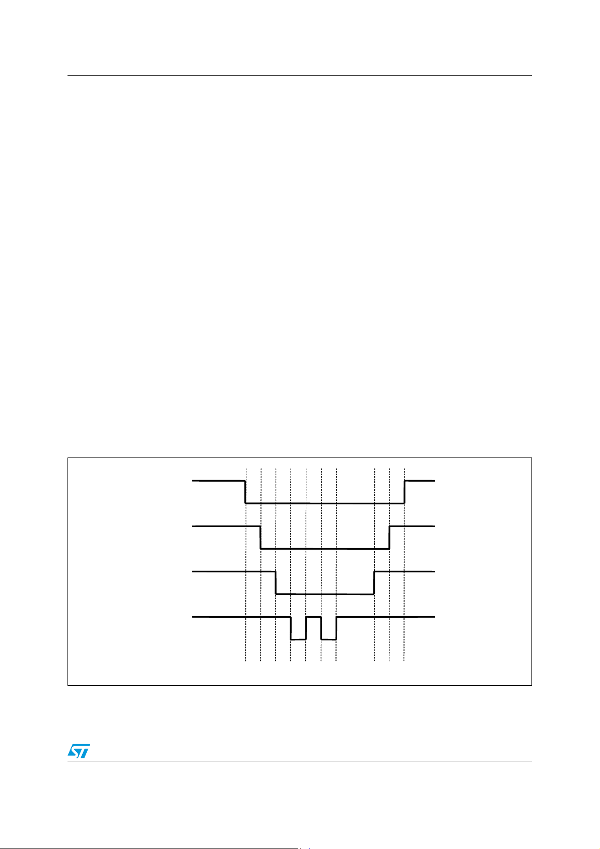
STPMC1 Theory of operation
the SCS status. If SCS is low, SCLNCL is the input of serial bit synchronization clock signal.
When SCS is high, SCLNLC determines idle state of the SPI.
SDATD: is the data pin. If SCS is low, the operation of SDATD is dependent on the status of
SYN pin. If SYN is high SDATD is the output of serial bit data (read mode) if SYN is low
SDATD is the input of serial bit data signal (write mode). If SCS is high SDATD is input of
idle signal.
Any of the pins above has an internal weak pull-up device of a nominal 15 A. This means
that when a pin is not forced by external signals, the state of the pin is logic high. A high
state of any of the input pins above is considered in an idle (not active) state.
For the SPI to operate correctly the STPMC1 must be correctly supplied as described in the
power supply section. Idle state of SPI module is recognized when the signals of pins SYN,
SCS, SCLNLC and SDATD are in a logic high state. Any SPI operations should start from
such an idle state. The exception to this rule is when the STPMC1 has been put into
standalone application mode. In this mode it is possible that the states of the pins SCLNLC,
SDATD and SYN are not high due to the states of the corresponding internal status bits.
When SCS is active (low), signal SDATD should change its state at the trailing edge of the
signal SCLNLC and signal SDATD should be stable at the next leading edge of signal
SCLNLC. The first valid bit of SDATD is always started with activation of signal SCLNLC.
9.21.1 Remote reset
The timing diagram of the operation is shown in remote reset request timing. The time step
can be as short as 30 ns.
The internal reset signal is called RRR. Unlike the POR, the RRR signal does not cause the
125 ms delayed restart of the digital module. This signal does not clear the mode signals.
Figure 21. Timing for providing remote reset request
SCS
SCS
SYN
SYN
SCLNLC
SCLNLC
SDATD
SDATD
t1t2t3t4t5t6t
t1t2t3t4t5t6t
Note: All the time intervals must be longer than 30 ns.
t
-> t8 is the reset time, this interval must be longer than 30 ns as well.
7
Doc ID 15728 Rev 6 61/77
t8t9t
7
7
t8t9t
10
10
Page 62

Theory of operation STPMC1
9.21.2 Reading data records
Data record reading takes place most often when there is an on-board microcontroller in an
application. This microcontroller is capable of reading all measurement results and all
system signals (configuration, calibration, status, mode). Again, the time step can be as
short as 30 ns. There are two phases of reading, called latching and shifting.
Latching is used to sample results into transmission latches. The transmission latches are
the flip-flops that hold the data in the SPI interface. This is done with the active pulse on
SYN when SCS is idle. The length of pulse on SYN must be longer than 2 periods of
measurement clock, i.e. more than 500 ns at 4 MHz.
The shifting starts when SCS become active. In the beginning of this phase another, but
much shorter, pulse (30 ns) on SYN should be applied in order to ensure that an internal
transmission serial clock counter is reset to zero. An alternative way is to extend the pulse
on SYN into the second phase of reading. After that reset is done, a 32 serial clocks per
data record should be applied. Up to 8 data records can be read this way. This procedure
can be aborted at any time by deactivation of SCS.
The timing diagram of the reading operation is shown in timing for data records reading. One
can see the latching and beginning of shifting phase of the first byte of the first data record
and end of reading.
Figure 22. Timing for data records reading
SCS
SCS
SYN
SYN
SCLNLC
SCLNLC
SDATD
SDATD
t1t
t1t
2
2
t
t
t
t
3
3
t
t
t
t
4
4
6
6
5
5
t1 −> t2: Latching Phase. Interval value > 2/f
t
−> t
: Data latched, SPI idle. Interval value > 30 ns.
2
3
t
−> t4: Enable SPI for read operation. Interval value > 30 ns.
3
t
−> t5: Serial clock counter is reset. Interval value > 30 ns.
4
t
−> t6: SPI reset and enabled for read operation. Interval value > 30 ns
5
t
: Internal data transferred to SDATD
7
t
: SDATD data is stable and can be read
8
t7t
t7t
f(read)
f(read)
1st byte
1st byte
8
8
CLK
last bit of 32nd byte
last bit of 32nd byte
62/77 Doc ID 15728 Rev 6
Page 63

STPMC1 Theory of operation
The first read out byte of the data record is the least significant byte (LSB) of the data value
and of course, the fourth byte is the most significant byte (MSB) of the data value. Each byte
can be further divided into a pair of 4-bit nibbles, most and least significant nibble (msn, lsn).
This division makes sense with the MSB of the data value because the msn holds the parity
code.
Figure 23. Data records reconstruction
The sequence of the data record during the reading operation is fixed. However, an
application may apply a precharge command (see mode signal description) prior to the
reading phase. This command increases the group pointer forcing the device to respond
with the next group data records sequence.
The system that reads the data record from the STPMC1 should check the integrity of each
data record, as indicated in paragraph
repeated, but this time only the shifting should be applied; otherwise new data would be
latched into transmission latches, thus losing the previous reading.
Normally, each byte is read out as the most significant bit (msb) first. But this can be
changed by setting the MSBF configuration bit in the STPMC1 CFL data record. If this is
done, each byte is read out as the least significant bit (lsb) first.
9.21.3 Writing procedure
Each writable bit (configuration and mode bits) has its own 7-bit absolute address. For the
configuration bits, the 7-bit address value corresponds to its decimal value, while for the
mode bits the addresses are those indicated in the mode signal paragraph.
In order to change the state of a latch one must send to the STPMC1 a byte of data which is
the normal way to send data via SPI. This byte consists of 1-bit data to be latched (msb),
followed by 7-bit address of destination latch, which makes total 8 bits of command byte, as
summarized in the table below.
9.17.8
. If the check fails, the reading should be
Doc ID 15728 Rev 6 63/77
Page 64

Theory of operation STPMC1
Table 35. Functional description of commands
Bit pos.
76543210
Command
(X, D, A = {0, 1})
D0000000 CFG000=D, (shadow of first configurator, TSTD)
DAAAAAAA CFGa=D, (shadow of any configurator, a = AAAAAA
D1101111 CFG111=D, (shadow of last configurator, CHK)
Example 18: Setting a configuration bit
To set the configuration bit 47 (part of the R-phase current channel calibrator) to 0, we
must convert the decimal 47 to its 7-bit binary value: 0101111. The byte command is
then composed like this:
1 bit DATA value+7-bits address = 10101111 (0xAF)
The same procedure should be applied for the mode signals, but in this case the 7-bits
address must be taken from the relative
The lsb of command is also called EXE bit because instead of a data bit value, the
corresponding serial clock pulse is used to generate the necessary latching signal. This way
the writing mechanism does not need the measurement clock in order to operate, which
makes the operation of SPI module of STPMC1 completely independent from the rest of
device logic except from the signal POR.
Ta bl e 34
.
< 11100002)
2
Commands for changing system signals should be sent during active signals SCS and SYN
as it is shown in
Figure 24
. The SYN must be put low in order to disable SDATD output
driver of STPMC1 and make the SDATD as an input pin. A string of commands can be send
within one period of active signals SCS and SYN or command can be followed by reading
the data record but, in this case, the SYN should be deactivated in order to enable SDATD
output driver and a SYN pulse should be applied before activation of SCS in order to latch
the data.
Figure 24. Timing for writing configuration and mode bits
SCS
SCS
SYN
SYN
SCLNLC
SCLNLC
SDATD
SDATD
t1t2t3t4t
t1t2t3t4t
5
5
t
t
6
6
t8t
t
t8t
t
7
7
9
9
t1 −> t2 (> 30 ns): SPI out of idle state
t
−> t3 (> 30 ns): SPI enabled for write operation
2
64/77 Doc ID 15728 Rev 6
Page 65

STPMC1 Theory of operation
t3: data value is placed in SDA
t
: SDA value is stable and shifted into the device
4
t
−> t5 (> 10 µs): writing clock period
3
t
−> t5: 1 bit data value
3
t
−> t6: 6 bits address of the destination latch
5
t
−> t7: 1 bit EXE command
6
t
: end of SPI writing
8
t
: SPI enters idle state
9
9.21.4 Interfacing the standard 3-wire SPI with STPMC1 SPI
Due to the fact that a 2-wire SPI is implemented in the STPMC1, it is clear that sending any
command from a standard 3-wire SPI would require 3-wire to 2-wire interface, which should
produce a proper signal on SDATD from host signals SDI, SDO and SYN. A single gate 3state buffer could be omitted by an emulation of SPI just to send some command. On a
microcontroller this would be done by the following steps:
1. disable the SPI module
2. set SDI pin which is connected to SDATD to be output
3. activate SYN first and then SCS
4. apply new bit value to SDI and activate SCL
5. deactivate SCL
6. repeat the last two steps seven times to complete one byte transfer
7. repeat the last three steps for any remaining byte transfer
8. set SDI pin to be input
9. deactivate SCS and the SYN
10. enable the SPI module
In case of precharge command (0xFF), emulation above is not necessary. Due to the pull up
device on the SDATD pin of the STPMC1 the processor needs to perform the following
steps:
1. activate SYN first in order to latch the result;
2. after at least 1 s activate SCS
3. write one byte to the transmitter of SPI (this produces 8 pulses on SCL with SDI = 1)
4. deactivate SYN
5. optionally read the data records (the sequence of reading is altered
6. deactivate SCS
9.21.5 Permanent writing of the CFG bits
In order to make a permanent set of some CFG bits, the following procedure should
be conducted:
Doc ID 15728 Rev 6 65/77
Page 66

Theory of operation STPMC1
1. collect all addresses of CFG bits to be permanently set into some list
2. clear all OTP shadow latches
3. set the system signal RD
4. connect a current source of at least +14 V, 1 mA to 3 mA to VOTP
5. wait for VOTP voltage is stable
6. set one OTP shadow latch from the list
7. set the system signal WE
8. wait for 300 µs
9. clear the system signal WE
10. clear the OTP shadow latch which was set in step 6
11. until all wanted CFG bits are permanently set, repeat steps 5 to 11
12. disconnect the current source
13. wait for VOTP voltage is less than 3V
14. clear the system signal RD
15. read all data records, in the last two of them there is read back of CFG bits
16. if verification of CFG bits fails and there is still chance to pass, repeat steps 1 to 16
For set or clear steps, apply the timing shown in timing for data records reading with proper
signal on the SDATD. For step 15, apply the timing shown in timing for writing configuration
and mode bits.
For permanent set of the TSTD bit, which causes no more writing to the configuration bits,
the procedure above must be conducted in such way that steps 6 to 13 are performed in
series during single period of active SCS because the idle state of SCS would make the
signal TSTD immediately effective which in turn, would abort the procedure and possibly
destroy the device due to clearing of system signal RD and so, connecting all gates of 3 V
NMOS sense amplifiers of already permanently set CFG bits to the VOTP source.
66/77 Doc ID 15728 Rev 6
Page 67

STPMC1 Energy calculation algorithm
10 Energy calculation algorithm
For the purpose of simplicity the energy computation shown below is relative to only one
phase.
Given line voltage and current as:
Equation 12
u = U sin (ω t) i = I sin(ω t + ϕ)
The voltage divider, AD converter and calibrator produce the value:
Equation 13
v
= u (R2/(R1+R2) (AU/V
u
The Rogowski coil preamplifier, AD converter and calibrator produce the value:
Equation 14
v
= - L (di/dt) (AI/V
i
The 2
nd
stage internal integrations produce the values:
REF
) kU = u kD = A sin (ω t)
REF
) kI = - I kL ω cos (ω t + ϕ) = - B ω cos (ω t + ϕ)
Equation 15
v
= ∫ vudt = - (A / ω) cos (ω t) k
ui
INT
Equation 16
vii = ∫ v
dt = - B sin (ω t + ϕ) k
i
INT
From signs of vu and vui the base frequency of line can be produced:
Equation 17
ω / k
INT
= k / T
This result is used to compensate Eq. 41, Eq. 44, Eq. 45 and Eq. 54.
The frequency compensated values are:
Equation 18
v
= ω / k
uic
= - A cos (ω t)
INT vui
Equation 19
v
= ω / k
iic
The 3
rd
stage internal integrations and DC cancellations produce the values:
= - B ω sin (ω t + ϕ)
INT vii
Equation 20
v
uiic
= ∫ v
dt = - (A / ω) sin (ω t) k
uic
Equation 21
v
= ∫ v
iiic
dt = B cos (ω t + ϕ) k
iic
INT
INT
Doc ID 15728 Rev 6 67/77
Page 68

Energy calculation algorithm STPMC1
In case of shunt sensor (TCS = 1), an additional stage of internal digital differentiated
produces the value:
Equation 22
v
= dvu/dt = A ω cos (ω t) k
d
DIF
The shunt preamplifier, AD converter and calibrator produce the value:
Equation 23
vs = i R
The 2
(AI/V
S
nd
stage internal integrations produce the values:
) kI = i kS = C sin (ω t + ϕ)
REF
Equation 24
v
= ∫ vddt = A sin (ω t) k
di
DIF kINT
= A sin (ω t)
Equation 25
v
= ∫ vsdt = - (C / ω) cos (ω t + ϕ) k
si
INT
The frequency compensated values are:
Equation 26
V
= ω / k
dic
= A ω sin (ω t) / k
INT vdi
INT
Equation 27
v
= ω / k
sic
The 3
rd
stage internal integrations and DC cancellations produce the values:
= - C cos (ω t + ϕ)
INT vsi
Equation 28
v
diic
= ∫ v
dt = A cos (ω t) k
dic
DIF kINT
= A cos (ω t)
Equation 29
v
siic
= ∫ v
dt = - (C / ω) sin (ω t + ϕ) k
sic
INT
10.1 Active energy calculation
The active power is computed as follows.
First, the voltage stream from the 1
16-bit current from the 2
st
1
stage (
filter (
Equation 14
Equation 15
nd
or
or
Equation 24
stage (
Equation 23
Equation 30
P
= vu vii = - ABk
1
sin (ω t) sin (ω t + ϕ) = - ABk
INT
Equation 31
P
= vui vi = ABk
2
68/77 Doc ID 15728 Rev 6
cos (ω t) cos (ω t + ϕ) = ABk
INT
st
stage (
Equation 16
Equation 13
or
) is multiplied to 16-bit voltage from the 2nd stage of
), yielding:
or
Equation 22
Equation 25
[cos ϕ - cos (2 ω t + ϕ)] / 2
INT
[cos ϕ + cos (2 ω t + ϕ)] / 2
INT
) and current stream from the
) is multiplied to the
Page 69

STPMC1 Energy calculation algorithm
In case of a non Rogowski sensor, the corresponding products are:
Equation 32
P
= vd vsi = - AC k
1
cos (ω t) cos (ω t + ϕ) = - AC [cos ϕ + cos (2 ω t + ϕ)] / 2
DIFkINT
Equation 33
P
= vdi vs = AC k
2
DIFkINT
Then a subtraction of P
sin (ω t) sin (ω t + ϕ) = AC [cos ϕ - cos (2 ω t + ϕ)] / 2
from P2 is performed:
1
Equation 34
P = (P
- P1) / 2 = (AB cos ϕ) k
2
/ 2 = (UkDIkL cos ϕ) k
INT
INT
/ 2 = U
RMS IRMS
cos ϕ k
P
where:
Equation 35
k
= kD kL k
P
This gives the same result for P in case of non Rogowski sensor, substituting B and kL k
with C and k
INT
S
:
INT
Equation 36
P = (P
- P1) / 2 = (AC cos ϕ) / 2 = (UkDIkS cos ϕ) / 2 = U
2
RMS IRMS
cos ϕ k
P
where:
Equation 37
k
= kD k
P
The result in
S
Equation 35
and
Equation 36
is proportional to the DC part of active power of
line. The division by 2 is a feature of ΔΣ subtractor. The absence of harmonic components
eliminates the spread of results due to asynchronism with the line. This fact enables fast a
calibration procedure which is used to set the target constant of meter k
A sensitivity analysis of k
yields:
P
.
P
Equation 38
Δk
= ΔL/L + R1 / (R1+R2)(ΔR2/R2 - ΔR1/R1) + ΔAU/AU + ΔAI/AI - 2 ΔV
P/kP
Equation 39
Δk
= ΔRS / RS + R1 / (R1+R2)(ΔR2/R2 - ΔR1/R1) + ΔAU/AU + ΔAI/AI - 2 ΔV
P/kP
It is clear that the device is responsible for AU, AI and V
are omitted, because they are not subject to aging or temperature variations due to digital
implementation.
10.2 Reactive energy calculation
The natural reactive power (ART = 0) of the line is computed as follows.
First, 16-bit voltage from the 3
current stream from the 1
rd
stage (
st
stage (
Doc ID 15728 Rev 6 69/77
Equation 20
Equation 14
or
or
Equation 23
REF/VREF
parts. The parts kU, kI and k
REF
Equation 28
) is multiplied by the
) and the frequency
REF/VREF
INT
Page 70

Energy calculation algorithm STPMC1
compensated stream of 16-bit voltage from the 2nd stage of filter (
26
) is multiplied by the 16-bit current stream from the 2nd stage (
25
) yielding:
Equation 18
Equation 16
or
Equation
or
Equation
Equation 40
Q
1
= v
uiic vi
= ABk
sin (ω t) cos (ω t + ϕ) = - ABk
INT
[sin ϕ - sin (2 ω t + ϕ)] / 2
INT
Equation 41
Q
= ω / k
2
INT vui vii
= ABk
cos (ω t) sin (ω t + ϕ) = ABk
INT
[sin ϕ + sin (2 ω t + ϕ)] / 2
INT
In case of non Rogowski sensor, the corresponding products are:
Equation 42
Q
1
= v
diic vs
= ACk
DIFkINT
cos (ω t) sin (ω t + ϕ) = AC [sin ϕ + sin (2 ω t + ϕ)] / 2
Equation 43
Q
= ω / k
2
INT vdi vsi
Then a subtraction of Q
= - ACk
DIFkINT
from Q2 is performed:
1
sin (ω t) cos (ω t + ϕ) = - AC [sin ϕ - sin (2 ω t + ϕ)] / 2
Equation 44
Q = (Q
- Q1) / 2 = (AB sin ϕ) k
2
/ 2 = (UkDIkL sin ϕ) k
INT
INT
/ 2 = U
RMS IRMS
sin ϕ k
P
This gives the same result for Q in case of non Rogowski sensor, substituting B and kLk
with C and k
:
S
INT
Equation 45
Q = (Q
- Q1) / 2 = (AC sin ϕ) = (UkDIkS sin ϕ) / 2 = U
2
RMS IRMS
sin ϕ k
P
The artificial reactive power (ART = 1) of line is computed as follows.
The inter-phase voltage sigma-delta stream is computed from voltage stream from the 1
stage as follows:
Equation 46
Δv
= (v
uR
Δv
= (v
uS
Δv
= (v
uT
The inter-phase voltage sigma-delta stream (
stage (
- vuT) / 2
uS
- vuR) / 2
uT
- vuS) / 2
uR
Equation 16
or
Equation 25
Equation 46
), the 16-bit current from the 2nd
) and the value of 1 / √3 are multiplied yielding:
Equation 47
Q = Δv
1 / √3 = AB k
u vii
[sin ϕ + sin (2 ω t + ϕ)] / 2
INT
or in case of non Rogowski sensor, the corresponding products are:
Equation 48
Q = Δv
1 / √30 = AC [sin ϕ + sin (2 ω t + ϕ)] / 2
d vsi
st
70/77 Doc ID 15728 Rev 6
Page 71

STPMC1 Energy calculation algorithm
10.3 Voltage and current RMS values calculation
The I
value is produced from 16-bit value of
RMS
Equation 16
:
Equation 49
T
2
I
RMSkLkINT
The Ui
1
=
is produced from stream and 16-bit value of
RMS
dt
v
∫
ii
T
0
= B
1
2
Equation 15
:
Equation 50
T
Ui
RMSkD
=
2
1
∫
T
0
v
= Ak
dt
ui
INT
/ω
1
2
In case of non Rogowski sensor, the same dedicated RMS blocks produce some other
values, because input values for the blocks are changed.
Therefore, another RMS value, named Ii
is produced from 16-bit value of
RMS
Equation 25
Equation 51
T
Ii
RMSkSkINT
=
2
1
T
= C/ω
dt
v
∫
si
0
1
2
:
The U
is produced from stream and 16-bit value of
RMS
Equation 52
T
2
=
1
∫
T
0
v
= A
dt
di
U
RMSkD
10.4 Energy integration
The internal hard-wired DSP unit performs all the computations above in real time for a
power line in parallel by means of arithmetic blocks. Due to implementation of an integrator,
up/down counter or deviator, part of which is also an integrator in a feedback, additional
factors are introduced into computations. If we declare f
frequency and M as number of possible values of some integrator, the following constant
factors can be defined:
Equation 53
k
= 2 f
INT
kUD = 2 f
k
= M
DIF
MCLK
MCLK
/ 2 f
DIF
/ M
/ MUD = 2
MCLK
INT
= 2
= 2
8
11
-8
Equation 24
1
2
MCLK
:
as the measurement clock
Doc ID 15728 Rev 6 71/77
Page 72

Energy calculation algorithm STPMC1
The DSP performs also an integration of powers (P, Q) into energies:
Equation 54
AW = U
RMS IRMS
cos ϕ kP k
UD
Equation 55
AW = U
RMS IRMS
sin ϕ kP k
UD
These integrators are implemented as up/down counters and they can roll over.
20-bit output buses of the counters are assigned as the most significant part of the energy
data records. It is a responsibility of the application to read the counters at least every
second so as not to miss any rollover. The integration of power can be suspended due to
detected error on the source signals or due to no load condition. From AW, stepper output
signals are generated.
10.5 Fundamental power calculation
The fact that integration suppresses all but fundamental components of signals is used to
compute the fundamental active power, which is in case of Rogowski coil:
Equation 56
F
= v
1
Equation 57
F
= v
2
uic viiic
iic vuiic
= - ABk
= - ABk
cos (ω t) cos (ω t + ϕ) = - ABk
INT
sin (ω t) sin (ω t + ϕ) = ABk
INT
[cos ϕ + cos (2 ω t + ϕ)] / 2
INT
[cos ϕ - cos (2 ω t + ϕ)] / 2
INT
Equation 58
F = (F
- F1) / 2 = (AB cos ϕ) k
2
/ 2 = (UkDIkLcos ϕ) k
INT
/ 2 = U
INT
Similar result are found in case of non Rogowski sensor:
Equation 59
F
= v
1
dic vsiic
= - AC sin (ω t) sin (ω t + ϕ) = - AC [cos ϕ - cos (2 ω t + ϕ)] / 2
Equation 60
F
= v
2
sic vdiic
= - ACk
DIFkINT
cos (ω t) cos (ω t + ϕ) = - AC [cos ϕ + cos (2 ω t + ϕ)] / 2
Equation 61
F = (F
ϕ) k
- F1) / 2 = - AC cos (2 ω t + ϕ) = UkDIks cos (2 ω t + ϕ) / 2 = U
2
P
The fundamental reactive power in case of a Rogowski coil is:
Equation 62
Q = v
uiic viiic
ω / k
INT
= - ABk
cos (ω t) sin (ω t + ϕ) = ABk
INT
INT
Similar results are found in cases of non Rogowski sensors:
Equation 63
Q = v
diic vsiic
ω / k
= - AC cos (ω t) sin (ω t + ϕ) = AC [sin ϕ - sin (2 ω t + ϕ)] / 2.
INT
RMS IRMS
cos ϕ k
RMS IRMS
P
cos (2 ω t +
[sin ϕ - sin (2 ω t + ϕ)] / 2
72/77 Doc ID 15728 Rev 6
Page 73

STPMC1 Package mechanical data
11 Package mechanical data
In order to meet environmental requirements, ST offers these devices in different grades of
ECOPACK
specifications, grade definitions and product status are available at:
ECOPACK
®
packages, depending on their level of environmental compliance. ECOPACK®
®
is an ST trademark.
www.st.com
.
Doc ID 15728 Rev 6 73/77
Page 74

Package mechanical data STPMC1
TSSOP20 mechanical data
mm. inch.
Dim.
Min. Typ. Max. Min. Typ. Max.
A 1.2 0.047
A1 0.05 0.15 0.002 0.004 0.006
A2 0.8 1 1.05 0.031 0.039 0.041
b 0.19 0.30 0.007 0.012
c0.09 0.20 0.004 0.0079
D 6.4 6.5 6.6 0.252 0.256 0.260
E 6.2 6.4 6.6 0.244 0.252 0.260
E1 4.3 4.4 4.48 0.169 0.173 0.176
e 0.65 BSC 0.0256 BSC
K0° 8°0° 8°
L 0.45 0.60 0.75 0.018 0.024 0.030
A2
A
A1
b
e
K
c
L
E
D
E1
PIN 1 IDENTIFICATION
1
74/77 Doc ID 15728 Rev 6
0087225C
Page 75

STPMC1 Package mechanical data
Tape & reel TSSOP20 mechanical data
mm. inch.
Dim.
Min. Typ. Max. Min. Typ. Max.
A 330 12.992
C 12.8 13.2 0.504 0.519
D 20.2 0.795
N60 2.362
T 22.4 0.882
Ao 6.8 7 0.268 0.276
Bo 6.9 7.1 0.272 0.280
Ko 1.7 1.9 0.067 0.075
Po 3 .9 4.1 0.153 0.161
P 11.9 12.1 0.468 0.476
Doc ID 15728 Rev 6 75/77
Page 76

Revision history STPMC1
12 Revision history
Table 36. Document revision history
Date Revision Changes
22-May-2009 1 Initial release.
03-Jul-2009 2 Updated: paragraphs
28-Jul-2009 3 Updated: paragraph
Added:
19-May-2010 4
11-Oct-2011 5 Updated: V
24-Apr-2012 6
system - BCS = 1 on page 31
Example 8: 1-ph system - BCS = 1 on page 31
Modified: paragraph
Modified: Supports IEC 62052-11 / 62053-21 / 62053-23 standards
on page 1
Added:
Example 5: 3-ph system - BCS = 0 on page 29, Example 6: 3-ph
and VIL values
IH
,
Table 11 on page 23
Table 12 on page 23
9.4, 9.16
9.16.2
9.17.2 on page 47
and
9.17.8
.
,
Example 7: 1-ph system - BCS = 0 on page 31
Table 7 on page 13
and
Table 23 on page 41
.
.
,
and
Equation 11: on page 48
.
.
Features
.
.
76/77 Doc ID 15728 Rev 6
Page 77

STPMC1
Please Read Carefully:
Information in this document is provided solely in connection with ST products. STMicroelectronics NV and its subsidiaries (“ST”) reserve the
right to make changes, corrections, modifications or improvements, to this document, and the products and services described herein at any
time, without notice.
All ST products are sold pursuant to ST’s terms and conditions of sale.
Purchasers are solely responsible for the choice, selection and use of the ST products and services described herein, and ST assumes no
liability whatsoever relating to the choice, selection or use of the ST products and services described herein.
No license, express or implied, by estoppel or otherwise, to any intellectual property rights is granted under this document. If any part of this
document refers to any third party products or services it shall not be deemed a license grant by ST for the use of such third party products
or services, or any intellectual property contained therein or considered as a warranty covering the use in any manner whatsoever of such
third party products or services or any intellectual property contained therein.
UNLESS OTHERWISE SET FORTH IN ST’S TERMS AND CONDITIONS OF SALE ST DISCLAIMS ANY EXPRESS OR IMPLIED
WARRANTY WITH RESPECT TO THE USE AND/OR SALE OF ST PRODUCTS INCLUDING WITHOUT LIMITATION IMPLIED
WARRANTIES OF MERCHANTABILITY, FITNESS FOR A PARTICULAR PURPOSE (AND THEIR EQUIVALENTS UNDER THE LAWS
OF ANY JURISDICTION), OR INFRINGEMENT OF ANY PATENT, COPYRIGHT OR OTHER INTELLECTUAL PROPERTY RIGHT.
UNLESS EXPRESSLY APPROVED IN WRITING BY TWO AUTHORIZED ST REPRESENTATIVES, ST PRODUCTS ARE NOT
RECOMMENDED, AUTHORIZED OR WARRANTED FOR USE IN MILITARY, AIR CRAFT, SPACE, LIFE SAVING, OR LIFE SUSTAINING
APPLICATIONS, NOR IN PRODUCTS OR SYSTEMS WHERE FAILURE OR MALFUNCTION MAY RESULT IN PERSONAL INJURY,
DEATH, OR SEVERE PROPERTY OR ENVIRONMENTAL DAMAGE. ST PRODUCTS WHICH ARE NOT SPECIFIED AS "AUTOMOTIVE
GRADE" MAY ONLY BE USED IN AUTOMOTIVE APPLICATIONS AT USER’S OWN RISK.
Resale of ST products with provisions different from the statements and/or technical features set forth in this document shall immediately void
any warranty granted by ST for the ST product or service described herein and shall not create or extend in any manner whatsoever, any
liability of ST.
ST and the ST logo are trademarks or registered trademarks of ST in various countries.
Information in this document supersedes and replaces all information previously supplied.
The ST logo is a registered trademark of STMicroelectronics. All other names are the property of their respective owners.
© 2012 STMicroelectronics - All rights reserved
STMicroelectronics group of companies
Australia - Belgium - Brazil - Canada - China - Czech Republic - Finland - France - Germany - Hong Kong - India - Israel - Italy - Japan -
Malaysia - Malta - Morocco - Philippines - Singapore - Spain - Sweden - Switzerland - United Kingdom - United States of America
www.st.com
Doc ID 15728 Rev 6 77/77
 Loading...