

Page 1

second-order sigma-delta modulator with embedded PGLNA
Features
STPMS2
Smart sensor II dual-channel 1-bit, 4 MHz,
■ V
■ Two second-order sigma-delta (ΣΔ)
supply range 3.2 V - 5.5 V
CC
modulators
■ Programmable chopper-stabilized low noise
and low offset amplifier
■ Supports 50-60 Hz, EN 50470-1, EN 50470-3,
IEC 62053-21, IEC 62053-22 and IEC 6205323 standards specs for class 1, class 0.5 and
class 0.2 AC watt meters
■ STPM02H: less than 0.5% error over 1:10000
range
■ STPM02L: less than 0.5% error over 1:5000
range
■ Precision voltage reference: 1.23 V with
programmable TC (STPMS2L only)
■ Internal low drop regulator @ 3 V (typ.)
Applications
■ Power metering
■ Motor control
■ Industrial process control
■ Weight scales
■ Pressure transducers
QFN16 (4 x 4)
or multi-phase energy meters along with the
STPMC1 device, a digital signal processor
designed for energy measurement. This device
can be used in medium and high resolution
measurement applications where single or double
inputs must be monitored at the same time. The
STPMS2 are mixed signal ICs consisting of an
analog and digital section. The analog section
consists of a programmable gain, low noise
choppered amplifier, two second-order ΔΣ
modulator blocks, a band-gap voltage reference,
a low-drop voltage regulator and DC buffers, while
the digital section consists of a clock generator
and output multiplexer.
Description
The STPMS2, also called “smart sensor” devices,
are ASSPs designed for effective measurement in
power line systems utilizing Rogowski coil, current
transformer, Hall or shunt sensors. These devices
are designed as building blocks for single-phase
Table 1. Device summary
Order codes Package Packaging
STPMS2H-PUR QFN16 (4 x 4 mm) 4500 parts per reel
STPMS2L-PUR QFN16 (4 x 4 mm) 4500 parts per reel
October 2011 Doc ID 16525 Rev 3 1/33
www.st.com
33
Page 2

Contents STPMS2
Contents
1 Introduction . . . . . . . . . . . . . . . . . . . . . . . . . . . . . . . . . . . . . . . . . . . . . . . . 3
2 Internal block diagram . . . . . . . . . . . . . . . . . . . . . . . . . . . . . . . . . . . . . . . 4
3 Pin configuration . . . . . . . . . . . . . . . . . . . . . . . . . . . . . . . . . . . . . . . . . . . . 5
4 Maximum ratings . . . . . . . . . . . . . . . . . . . . . . . . . . . . . . . . . . . . . . . . . . . . 6
4.1 General operating conditions . . . . . . . . . . . . . . . . . . . . . . . . . . . . . . . . . . . 7
5 Application . . . . . . . . . . . . . . . . . . . . . . . . . . . . . . . . . . . . . . . . . . . . . . . . 11
6 Terminology . . . . . . . . . . . . . . . . . . . . . . . . . . . . . . . . . . . . . . . . . . . . . . . 14
6.1 Conventions . . . . . . . . . . . . . . . . . . . . . . . . . . . . . . . . . . . . . . . . . . . . . . . 14
6.2 Notation . . . . . . . . . . . . . . . . . . . . . . . . . . . . . . . . . . . . . . . . . . . . . . . . . . 14
7 Typical performance characteristics . . . . . . . . . . . . . . . . . . . . . . . . . . . 15
8 Theory of operation . . . . . . . . . . . . . . . . . . . . . . . . . . . . . . . . . . . . . . . . 17
8.1 General operation description . . . . . . . . . . . . . . . . . . . . . . . . . . . . . . . . . 17
8.2 Functional description of the analog part . . . . . . . . . . . . . . . . . . . . . . . . . 17
8.3 Functional description of the digital part . . . . . . . . . . . . . . . . . . . . . . . . . . 20
8.3.1 Decoder for different modes of operation . . . . . . . . . . . . . . . . . . . . . . . 21
8.3.2 Generator for clock frequency . . . . . . . . . . . . . . . . . . . . . . . . . . . . . . . . 21
8.4 Hard mode . . . . . . . . . . . . . . . . . . . . . . . . . . . . . . . . . . . . . . . . . . . . . . . . 21
8.5 Soft mode . . . . . . . . . . . . . . . . . . . . . . . . . . . . . . . . . . . . . . . . . . . . . . . . . 23
8.5.1 Writing to the configuration register in Soft mode . . . . . . . . . . . . . . . . . 27
9 Package mechanical data . . . . . . . . . . . . . . . . . . . . . . . . . . . . . . . . . . . . 28
10 Revision history . . . . . . . . . . . . . . . . . . . . . . . . . . . . . . . . . . . . . . . . . . . 32
2/33 Doc ID 16525 Rev 3
Page 3

STPMS2 Introduction
1 Introduction
The STPMS2 is a device designed to measure electrical line parameters (voltage and
current) via analog signals from voltage sensors (current divider) and current sensors
(inductive Rogowski coil, current transformer or shunt resistors). The device is used
together with a digital signal processing circuit to implement an effective measuring system
for multi-phase power meters.
The device consists of two analog measuring channels, consisting of second-order sigmadelta modulators with appropriate non-overlapping control signal generator. The STPMS2
also includes a temperature compensated band-gap reference voltage generator, a lowdrop supply voltage stabilizer and minimal digital circuitry that includes BIST (built-in selftest) structures. In a current signal processing channel, a low-noise preamplifier is included
in front of the sigma-delta converter. All reference voltages (band-gap, AGND) are internally
buffered to eliminate channel crosstalk.
The STPMS2 can operate in fast or low-power mode. In fast mode, a nominal clock
frequency of 4.1 or 4.9 MHz is applied to the clock input. In this mode, signal bandwidth is
specified between 0 and 4 kHz. In low-power mode, the nominal clock is four times slower in
order to reduce the power consumption of the circuit. In low-power mode, the quiescent bias
currents of the preamplifier and sigma-delta integrators are lowered and the signal
bandwidth is narrowed to the frequency bandwidth of 0 to 1 kHz.
Doc ID 16525 Rev 3 3/33
Page 4

Internal block diagram STPMS2
2 Internal block diagram
Figure 1. STPMS2 internal block diagram
VDDav
EINC HPV
VIP
VIN
CIP
CIN
VDDac
VCC
LDR
MUX
BIST D AC
MUX
EINC HPC
EINC HPC,
EINC HPV
GAIN
GAIN
PLNA
TC
VOLTAGE
REFERENCE
2nd ord ΣΔ
modulator
ECHPL FV,
PDV
ECHPHF V
EPRSV
EPRSV
ECHPL FC,
ECHPHFC
2nd ord ΣΔ
modulator
MV, NV
MC, NC
DIGITAL
VRefV
VRefC
FRONT
END
DAT
DATN
MS3
MS2
MS1
MS0
CLK
GND
VDDa
VBG
4/33 Doc ID 16525 Rev 3
AM09892v1
Page 5

STPMS2 Pin configuration
3 Pin configuration
Figure 2. Pin connections
MS3
CLK
13
MS2
12
MS1
11
VCC
VDDac
DAT
DATn
16
15
14
1
2
GND
10
9
MS0
VDDav
AM09382v1
Table 2. Pin description
VDDa
VBG
3
4
56
CIP
CIN
7
VIN
8
VIP
Pin n° Symbol Description
1 VCC Unregulated supply voltage for pad-ring, bandgap, low-drop and level shifters
2 VDDac Current channel modulator supply input
3 VDDa Output of internal + 3.0 V low drop regulated power supply
4 VBG
Output of internal + 1.23 V bias generator (STPMS2L);
Input of external precision reference voltage (STPMS2H)
5 CIN Current channel -
6 CIP Current channel +
7 VIN Voltage channel -
8 VIP Voltage channel +
9 VDDav Voltage channel modulator supply input
10 MS0 Input for configurator 0
11 MS1 Input for configurator 1
12 MS2 Input for configurator 2
13 MS3 Input for configurator 3
14 CLK Input for external measurement clock
15 DAT
16 DATn
Output of multiplexed ΣΔ signal
Output of current ΣΔ signal
Output of inverted multiplexed ΣΔ signal
Output of voltage ΣΔ signal
Exp PAD GND Ground level for signals and pin protection
Doc ID 16525 Rev 3 5/33
Page 6

Maximum ratings STPMS2
4 Maximum ratings
Table 3. Absolute maximum ratings
Symbol Parameter Value Unit
V
I
V
V
CC
PIN
ID
IA
DC Input voltage -0.3 to 6 V
Current on any pin (sink/source) ±150 mA
Input voltage at any pin -0.3 to V
+0.3 V
CC
Input voltage at analog pins (VIP, VIN, IIP, IIN) -0.7 to 0.7 V
ESD Human body model (all pins) ±2 kV
T
T
OP
T
J
STG
Operating ambient temperature -40 to 85 °C
Junction temperature -40 to 150 °C
Storage temperature range -55 to 150 °C
Note: Absolute maximum ratings are those values beyond which damage to the device may occur.
Functional operation under these conditions is not implied.
Table 4. Thermal data
Symbol Parameter Value Unit
(1)
R
thJA
1. This value is referred to single-layer PCB, JEDEC standard test board.
Thermal resistance junction-ambient 38.66 °C/W
6/33 Doc ID 16525 Rev 3
Page 7

STPMS2 Maximum ratings
4.1 General operating conditions
VCC = 5 V, T
between VBG and GND, f
Table 5. General operating conditions
= 25 °C, 1 µF between VCC, VDDa, VDDac, VDDav and GND, 100 nF
AMB
= 4.19 MHZ unless otherwise specified.
CLK
Symbol Parameter Test conditions Min. Typ. Max. Unit
General section
V
I
V
V
I
LATCH
f
Operating supply
CC
voltage
Quiescent current
CC
Power on reset on V
POR
Regulated supply
DD
voltage
LP, 1.229MHz; V
=3.3V; CL=100nF;
CC
no loads
HP, 4.915MHz; V
=3.2V; CL=100nF;
CC
no loads
CC
1.049MHz; VCC=3.2V; CL=100nF; no
loads
3.135 5.25 V
1.2 1.5
45
2.5 V
2.95 3.00 3.05 V
Current injection latchup immunity
Effective bandwidth Limited by chopper 0 4091 Hz
BW
300 mA
DC measurement accuracy
Resolution 11 16 bit
INL Integral non linearity
DNL Differential linearity
Offset error
Gain error
Result referred to a 16-bit word of CIPCIN channel, HP mode, f
= 2.047MHz
CLK
Result referred to a 12-bit word of VIPVIN channel, HP mode, f
=2.047MHz
CLK
Result referred to a 16-bit word of CIPCIN channel, HP mode, f
=2.047MHz
CLK
Result referred to a 12-bit word of VIPVIN channel, HP mode, f
=2.047MHz
CLK
Result referred to a 16-bit word of CIPCIN channel, HP mode, f
=2.047MHz
CLK
Result referred to a 12 bit-word of VIPVIN channel, HP mode, f
=2.047MHz
CLK
Result referred to a 16-bit word of CIPCIN channel, HP mode, f
=2.047MHz
CLK
Result referred to a 12-bit word of VIPVIN channel, HP mode, f
=2.047MHz
CLK
0.04 0.4
3.3
LSB
3.9
0.3
LSB
0.5
0.02
LSB
0.005
LSB/uV
0.003
CIP-CIN channel gain 2x 120
NF Noise floor
VIP-VIN channel 95
mA
dBCIP-CIN channel gain 16x 118
Doc ID 16525 Rev 3 7/33
Page 8

Maximum ratings STPMS2
Table 5. General operating conditions (continued)
Symbol Parameter Test conditions Min. Typ. Max. Unit
PSRR
Power supply DC
DC
rejection
AC measurement accuracy
SNR Signal to noise ratio
SINAD
Signal to noise ratio +
distortion
THD Total harmonic distortion
SFDR
PSRR
Spurious free dynamic
range
Power supply AC
AC
rejection
Analog inputs (CIP, CIN, VIP, VIN)
Voltage signal: 200 mV
Current signal: 10 mV
=2.048 MHz
f
CLK
rms
rms
/50Hz
/50Hz
VCC=3.3V ±10%, 5V ±10%
CIP-CIN channel – Vin=±230mV @
55Hz gain 2x over 4 kHz bandwidth
VIP-VIN channel – Vin=±230mV @
55Hz over 4 kHz bandwidth
CIP-CIN channel – Vin=±230mV @
55Hz gain 2x over 4 kHz bandwidth
VIP-VIN channel – Vin=±230mV @
55Hz over 4 kHz bandwidth
CIP-CIN channel – Vin=±230mV @
55Hz gain 2x over 4 kHz bandwidth
VIP-VIN channel – Vin=±230mV @
55Hz over 4 kHz bandwidth
CIP-CIN channel – Vin=±230mV @
55Hz gain 2x over 4 kHz bandwidth
VIP-VIN channel – Vin=±230mV @
55Hz over 4 kHz bandwidth
Voltage signal: 200 mV
Current signal: 10 mV
=2.048 MHz
f
CLK
VCC=3.3V+0.2V
=5.0V+0.2V
V
CC
rms
rms
/50Hz
rms
/50Hz
rms
1@100Hz
1@100Hz
90 dB
82
dB
52
82
dB
52
-105
dB
-78
90
dB
68
120 dB
VIP-VIN channel -0.3 +0.3 V
STPMS2L CIP-CIN channel
Gain 2x
Gain 4x
Gain 8x
V
Maximum input signal
MAX
levels
Gain 16x
STPMS2H CIP-CIN channel
f
V
Z
Z
G
A/D sampling frequency f
SPL
Amplifier offset ±20 mV
off
VIP, VIN impedance Over total operating voltage range 100 400 kΩ
IP
CIP, CIN impedance Over total operating voltage range 35 50 kΩ
IN
Gain error of current
ERR
channels
8/33 Doc ID 16525 Rev 3
-0.3
-0.15
-0.075
-0.0375
-V
REF
GAIN
+0.3
+0.15
+0.075
+0.0375
/
+V
REF
GAIN
CLK
±10 %
V
/
Hz
Page 9

STPMS2 Maximum ratings
Table 5. General operating conditions (continued)
Symbol Parameter Test conditions Min. Typ. Max. Unit
I
Voltage channel leakage
ILV
current
Current channel leakage
I
ILI
current
V
CC
V
CC
V
CC
=5.25V, f
=5.25V, f
=5.25V, f
CLK
CLK
CLK
enabled
Crosstalk between
channels
Digital I/O (CLK, DAT, DATN, MS0, MS1, MS2, MS3)
V
V
V
V
I
t
Input High voltage
IH
Input Low Voltage -0.3
IL
Output high voltage IO=-1mA, CL=50pF, VCC=3.2V VCC-0.4 V
OH
Output low voltage IO=+1mA, CL=50pF, VCC=3.2V 0.4 V
OL
Pull up current 15 µA
UP
Transition time C
TR
t
Latency From 50% of CLK to 50% to DAT 40 ns
L
=50pF 10 ns
LOAD
Clock input
Low precision mode 1.0 1.228
f
Nominal frequencies
CLK
Very high precision mode 4.0 4.915
=4.19MHz -1 1 µA
=4.19MHz -1 1
=4.19MHz input
-10 10
130 dB
0.75V
C
C
5.3 V
0.25V
C
C
MHzHigh precision mode 2.0 2.458
V
On chip reference voltage
V
Z
1. This level may be delivered from external source in STPMS2H.
Reference voltage STPMS2L only
REF
Output impedance 30 200 kΩ
out
I
Maximum load current 0 µA
L
Temperature coefficient After calibration 30 50 ppm/°C
T
C
(1)
Doc ID 16525 Rev 3 9/33
1.21 1.23 1.25 V
Page 10

Maximum ratings STPMS2
Figure 3. Timing diagram
AM09383v1
CLK - clock signal on CLK pin
CLK
bsV - sigma-delta bit stream of voltage signal
bsC - sigma-delta bit stream of current signal
DATA - multiplexed data of voltage and current signal on DAT pin
- sigma-delta sampling frequency
sample
10/33 Doc ID 16525 Rev 3
Page 11
STPMS2 Application
5 Application
The choice of external components in the transduction section of the application is a crucial
point in the application design, affecting the precision and the resolution of the entire
system.
Among the several considerations, a compromise should be found between the following
requirements:
1. Maximize the signal-to-noise ratio in the voltage and current channel
2. Choose the current-to-voltage conversion ratio Ks and the voltage divider ratio in a way
that calibration can be achieved
3. Choose Ks to take advantage of the whole current dynamic range in accordance with
desired maximum current and resolution.
To maximize the signal-to-noise ratio of the current channel, the voltage divider resistors
ratio should be as close as possible to those shown in Ta bl e 6 .
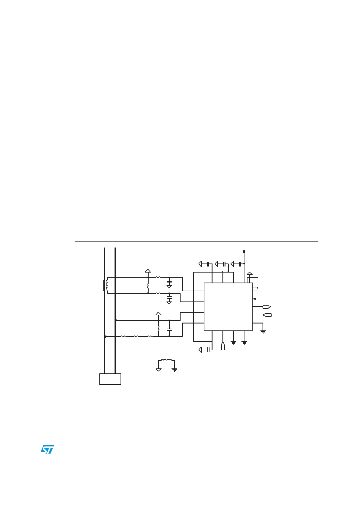
Figure 4 below provides a reference application schematic diagram:
● P = 64000 imp/kWh
● I
● I
Typical sensitivity values for the current sensors are indicated inTa bl e 6 .
NOM
MAX
= 5 A
= 60 A
Figure 4. Detailed application schematic
L
N
R7 1K 1%
C3
10n
L1 1µ
C7
4.7n
C8
4.7n
L3 E4622_X503
VN
VL
R2 150k
R3 150k
470 1%
R4 150k
R6
3.3 1%
R8 1K 1%
R5
LOAD
VCC
C5
C14
1µ
3
4
VBG
5
cin
6
cip
7
vin
8
vip
VDD av
9
C9
CLK
1µ
C6
1µ
1µ
VDD
DATn
DAT
CLK
MS3
e117e2
e3
e4
18
19
20
16
15
14
13
U1
STPMS2H/L
DAT
CLK
1
2
VDD a
VDD ac
MS010MS111MS2
12
MS0 = CLK HP Ampl x4
MS1 = 0 TC = 50 ppm/rC
MS2 = 0 Volta ge channel ON, DAT =(CLK)? bsV: bsC
MS3 = 0 Ha rdMode, BIST Mode OFF
AM09379v1
Doc ID 16525 Rev 3 11/33
Page 12
Application STPMS2
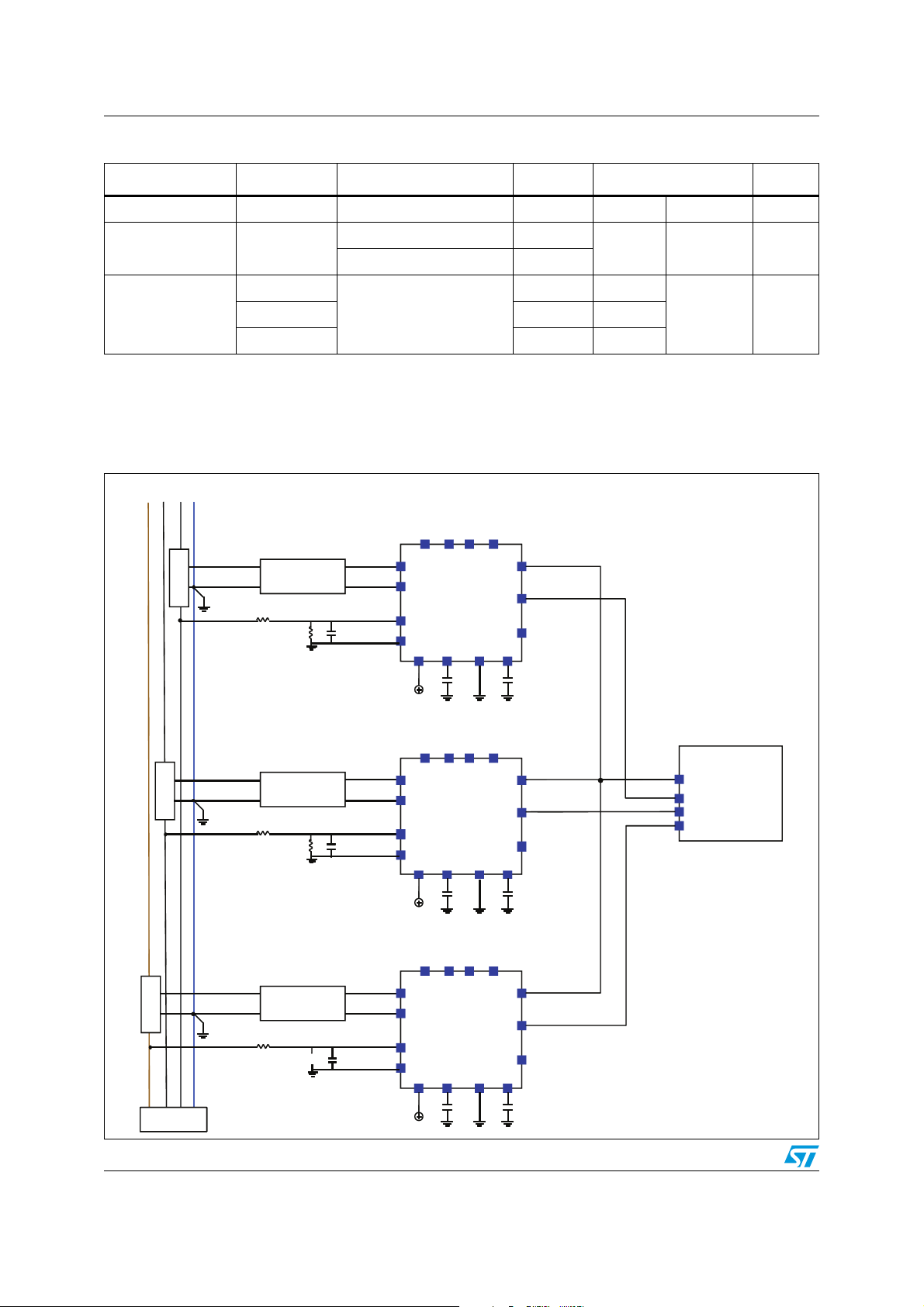
Table 6. Recommended external components in metering applications
Function Component Description Value Tolerance Unit
Calculator STPMC1 --- --- --- ---
Line voltage
interface
Line current
interface
Resistor
divider
Rogowski coil
R to R ratio V
R to R ratio V
Current-to-voltage ratio K
=230V 1:1650
RMS
=110V 1:830
RMS
S
±1% 50ppm/°C V/V
0.15 ±5%
50ppm/°C mV/ACT 1.7 ±5%
Shunt 0.43 ±5%
Note: Above listed components refer to typical metering application. Anyhow, STPMS2 operation
is not limited to the choice of these external components.
Figure 5. Simplified application schematics for STPMC1 based energy metering
R S T N
M S 1M S 0 M S 3M S 2
Ant i Al i a s i ng
Cur r ent
Sensor
Ne t wo r k
CIP
CIN
VIP
VIN
VBG
CLK
DAT
DAT n
GNDVCC VDD
M S 1M S 0 M S 3M S 2
Ant i Al i a s i ng
Cur r ent
Sensor
Current
Sensor
Ne t wo r k
Ant i Al i a s i ng
Ne t wo r k
CIP
CIN
VIP
VIN
CIP
CIN
VIP
VIN
VBG
M S 1M S 0 M S 3M S 2
VBG
CLK
DAT
DAT n
GNDVCC VDD
CLK
DAT
DAT n
GNDVCC VDD
LOAD
12/33 Doc ID 16525 Rev 3
CLK
DAT
DAS
DAR
Calc ulat or
STPM C1A
AM09893v1
Page 13
STPMS2 Application
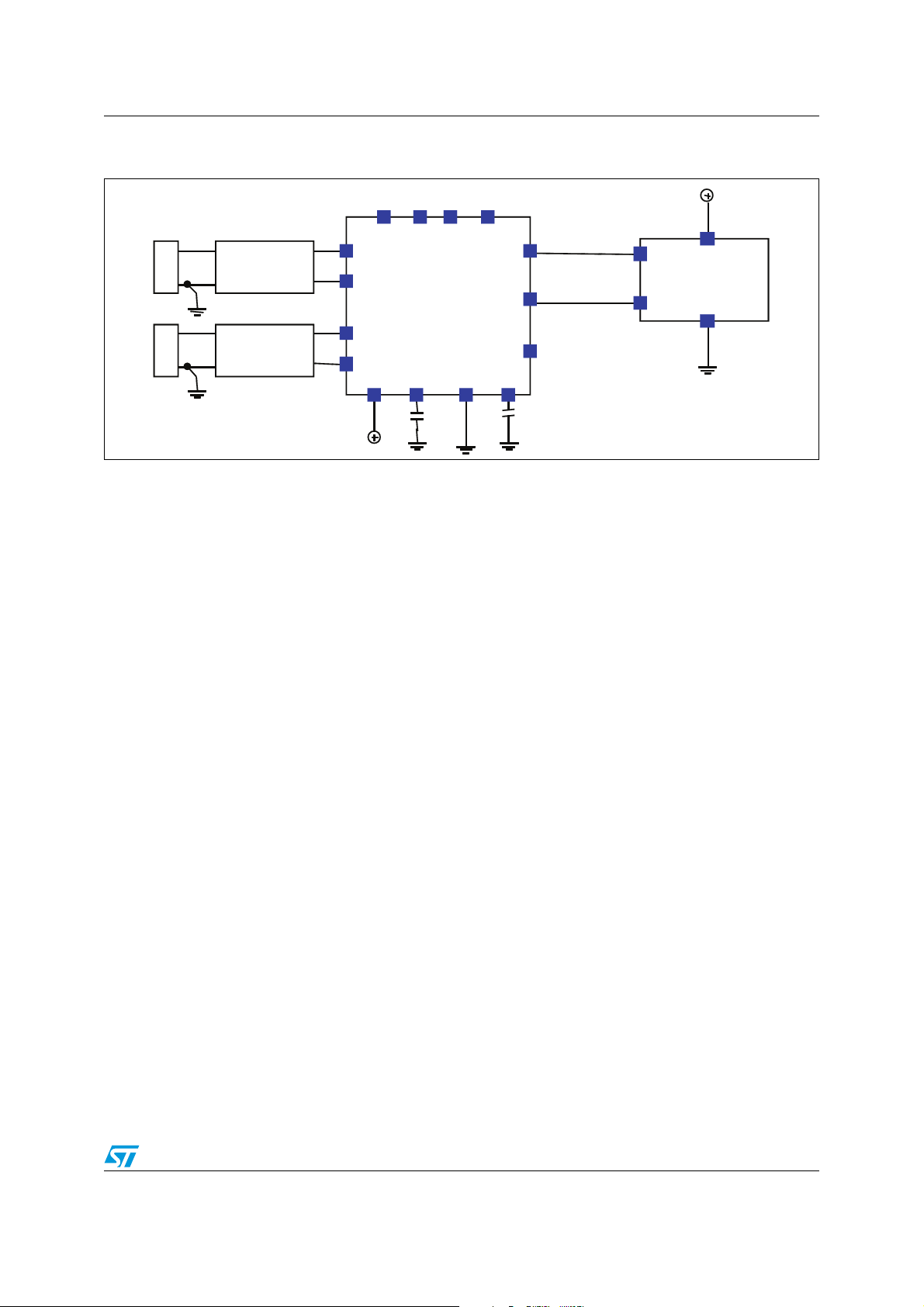
Figure 6. Connection schematics for DSP-based applications
MS1MS0MS3MS2
1
Sensor
Anti Al ias ing
Network
CIP
CIN
CLK
DAT
CLKOUT
DSP
DATIN
2
Sensor
Anti Al ias ing
Network
VIP
VIN
VBG
DATn
GNDVCC VDD
AM09380v1
Doc ID 16525 Rev 3 13/33
Page 14

Terminology STPMS2
6 Terminology
6.1 Conventions
The lowest analog and digital power supply voltage is called GND which represents the
system ground. All voltage specifications for digital input/output pins are referred to GND.
The highest power supply voltage is called V
generated and is called V
Positive currents flow into a pin. Sinking current means that the current is flowing into the pin
and thus it is positive. Sourcing current means that the current is flowing out of the pin and
thus it is negative.
A positive logic convention is used in all equations.
6.2 Notation
Output bit streams of the modulator are indicated as bsV and bsC for voltage and current
channels, respectively.
DD
.
. The highest core power supply is internally
CC
14/33 Doc ID 16525 Rev 3
Page 15
STPMS2 Typical performance characteristics
7 Typical performance characteristics
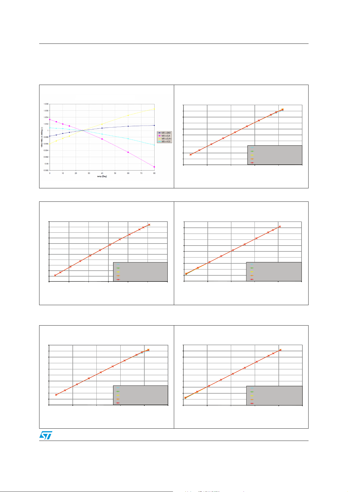
Figure 7. V
Figure 9. SNHR of I channel, gain 2x Figure 10. SNHR of V channel, gain 2x
90
80
70
60
50
40
30
SNHR [dB]
20
10
0
-10
-20
10 100 1000 10000 100000 1000000 10000000
REF/VREF
at 25 deg vs. temp Figure 8. SNHR of I channel, gain 16x
90
80
70
60
50
40
SNHR [dB]
30
I peak-peak [µV]
Current 2x, Fsig = 55Hz, HP mode 2.047MHz, 3.3V, -30deg
Current 2x, Fsig = 55Hz, HP mode 2.047MHz, 3.3V, 0deg
Current 2x, Fsig = 55Hz, HP mode 2.047MHz, 3.3V, 25deg
Current 2x, Fsig = 55Hz, HP mode 2.047MHz, 3.3V, 60deg
Current 2x, Fsig = 55Hz, LP mode 2.047MHz, 3.3V, 85deg
AM09902v1
20
10
0
-10
10 100 1000 10000 100000 1000000
60
50
40
30
20
10
SNHR [dB]
0
-10
-20
-30
-40
100 1000 10000 100000 1000000 10000000
I peak-peak [µV]
U peak-peak [µV]
Current 16x, Fsig = 55Hz, HP mode 2.047MHz, 3.3V, -30deg
Current 16x, Fsig = 55Hz, HP mode 2.047MHz, 3.3V, 0deg
Current 16x, Fsig = 55Hz, HP mode 2.047MHz, 3.3V, 25deg
Current 16x, Fsig = 55Hz, HP mode 2.047MHz, 3.3V, 60deg
Current 16x, Fsig = 55Hz, HP mode 2.047MHz, 3.3V, 85deg
Voltage 2x, Fsig = 55Hz, HP mode 2.047MHz, 3.3V, -30deg
Voltage 2x, Fsig = 55Hz, HP mode 2.047MHz, 3.3V, 0deg
Voltage 2x, Fsig = 55Hz, HP mode 2.047MHz, 3.3V, 25deg
Voltage 2x, Fsig = 55Hz, HP mode 2.047MHz, 3.3V, 60deg
Voltage 2x, Fsig = 55Hz, HP mode 2.047MHz, 3.3V, 85deg
AM09901v1
AM09903v1
Figure 11. SINAD of I channel, gain 16x (temp.
90
80
70
60
50
40
SINAD [dB]
30
20
10
0
-10
10 100 1000 10000 100000 1000000
variation)
I peak-peak [µV]
AM09904v1
Current 16x, Fsig = 55Hz, HP mode 2.047MHz, 3.3V, -30deg
Current 16x, Fsig = 55Hz, HP mode 2.047MHz, 3.3V, 0deg
Current 16x, Fsig = 55Hz, HP mode 2.047MHz, 3.3V, 25deg
Current 16x, Fsig = 55Hz, HP mode 2.047MHz, 3.3V, 60deg
Current 16x, Fsig = 55Hz, HP mode 2.047MHz, 3.3V, 85deg
Doc ID 16525 Rev 3 15/33
Figure 12. SINAD of I channel, gain 16x (temp.
variation)
60
50
40
30
20
10
SINAD [dB]
0
-10
-20
-30
-40
100 1000 10000 100000 1000000 10000000
U peak-peak [µV]
Voltage 2x, Fsig = 55Hz, HP mode 2.047MHz, 3.3V, -30deg
Voltage 2x, Fsig = 55Hz, HP mode 2.047MHz, 3.3V, 0deg
Voltage 2x, Fsig = 55Hz, HP mode 2.047MHz, 3.3V, 25deg
Voltage 2x, Fsig = 55Hz, HP mode 2.047MHz, 3.3V, 60deg
Voltage 2x, Fsig = 55Hz, HP mode 2.047MHz, 3.3V, 85deg
AM09905v1
Page 16
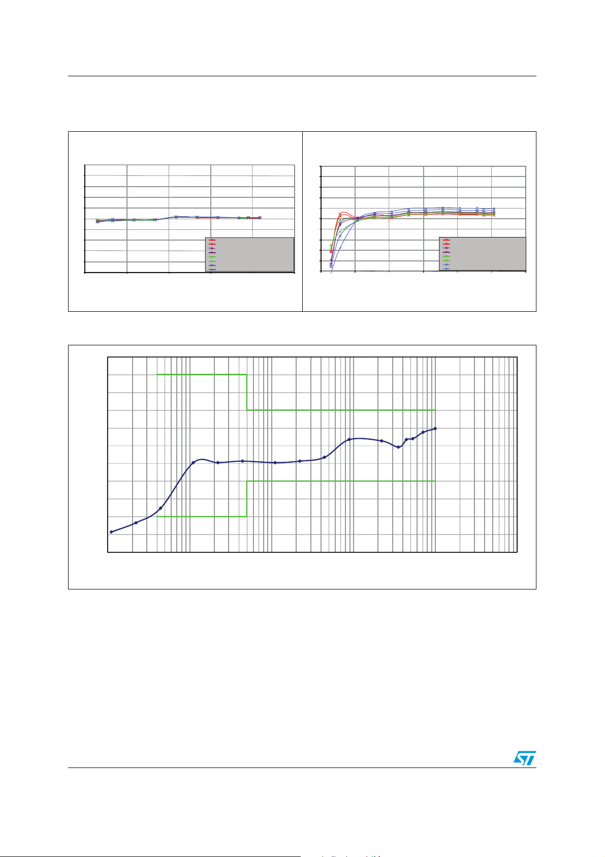
Typical performance characteristics STPMS2
Figure 13. Relative gain error of I channel,
1.1
1.08
1.06
1.04
1.02
1
0.98
Relative Gain Error [- ]
0.96
0.94
0.92
0.9
10 100 1000 10000 100000 1000000
Figure 15. Accuracy over dynamic range
0.5%
0.4%
0.3%
gain 16x
I peak-p eak [µV]
AM09899v1
Curr ent 32x, Fsig = 55Hz, HP mode 2.455MH z, 3.3V
Curr ent 32x, Fsig = 55Hz, HP mode 2.455MH z, 5.0V
Curr ent 32x, Fsig = 55Hz, HP mode 2.047MH z, 3.3V
Curr ent 32x, Fsig = 55Hz, HP mode 2.047MH z, 5.0V
Curr ent 32x, Fsig = 55Hz, LP mode 1.229MH z, 3.3V
Curr ent 32x, Fsig = 55Hz, LP mode 1.229MH z, 5.0V
Curr ent 32x, Fsig = 55Hz, LP mode 1.048MH z, 3.3V
Curr ent 32x, Fsig = 55Hz, LP mode 1.048MH z, 5.0V
Figure 14. Relative gain error of I channel,
gain 2x
1.1
1.08
1.06
1.04
1.02
1
0.98
Relative Gain Error [ - ]
0.96
0.94
0.92
0.9
10 100 1000 10000 100000 1000000 10000000
I peak-p eak [µV]
Curr ent 4x, Fsi g = 55H z, HP m ode 2.455MH z, 3.3V
Curr ent 4x, Fsi g = 55H z, HP m ode 2.455MH z, 5.0V
Curr ent 4x, Fsi g = 55H z, HP m ode 2.047MH z, 3.3V
Curr ent 4x, Fsi g = 55H z, HP m ode 2.047MH z, 5.0V
Curr ent 4x, Fsig = 55Hz, LP mode 1.229MHz , 3.3V
Curr ent 4x, Fsig = 55Hz, LP mode 1.229MHz , 5.0V
Curr ent 4x, Fsig = 55Hz, LP mode 1.048MHz , 3.3V
Curr ent 4x, Fsig = 55Hz, LP mode 1.048MHz , 5.0V
AM09906v1
AM09900v1
0.2%
0.035%
-0.008%
0.040%
0.076%
0.097%
Cla ss 0.2 limits
AW E rr o r [ %]
0.1%
0.0%
-0.1%
-0.2%
-0.3%
-0.4%
-0.487%
-0.435%
-0.352%
-0.096%
-0.096%
-0.087%
-0.096%
-0.087%
-0.065%
0.035%
0.027%
-0.5%
-0.6%
0.01% 0.10% 1.00% 10.00% 100.00% 1000.00%
% of FS
16/33 Doc ID 16525 Rev 3
Page 17

STPMS2 Theory of operation
8 Theory of operation
8.1 General operation description
The STPMS2 performs second-order analog modulation of two channels in parallel, with
appropriate non-overlapping control signal generator, of signals with frequencies varying
from DC to 4 kHz on two independent channels in parallel. The outputs of the converters
provide two streams of digital ones and zeros which can be then be multiplexed in time to
reduce the number of external connections.
The STPMS2 converts analog signals on two independent channels in parallel via deltasigma (ΣΔ) analog-to-digital converters into a binary stream of sigma-delta signals. The
device is particularly suitable to measure electrical line parameters (voltage and current) via
analog signals from voltage sensors (current divider) and current sensors (inductive
Rogowski coil, current transformer or shunt resistors). There is a current channel for
measuring line current and a voltage channel for measuring line voltage. The current
channel input is connected through an external anti-aliasing RC filter to a Rogowski coil,
current transformer (CT) or shunt current sensor which converts line current into an
appropriate voltage signal. The current channel includes a low-noise voltage preamplifier
with programmable gain. The voltage channel is connected directly through a resistor
voltage divider and anti-aliasing filter to a line voltage modulator (ADC). Both channels have
quiescent zero signal point at GND, so the STPMS2 is able to sample differential signals on
both channels with their zero point around GND.
The converted ΣΔ signals are multiplexed in time in order to reduce the number of external
connections. The conversion and the multiplex are driven by external clock signal CLK.
The device is used in conjunction with a digital signal processing circuit to implement an
effective measuring system of a multi-phase power meter.
The STPMS2 also includes a temperature compensated band-gap reference voltage
generator, low-drop supply voltage regulator and minimal digital circuitry that includes BIST
(built-in self-test) structures. In a current signal processing channel, a low-noise preamplifier
is included upstream of the sigma-delta converter. All reference voltages are designed to
eliminate channel crosstalk.
The STPMS2 can operate in fast (HP) or low-power (LP) mode (see also Ta bl e 7 ). In fast
mode, a nominal clock frequency of up to 4.1 / 4.9 MHz is applied to the clock input. In this
mode, signal bandwidth is specified between 0 and 4 kHz. In low-power mode, the nominal
clock is four times slower (1 MHz) to lower the power consumption of the circuit. In lowpower mode, the quiescent bias currents of the preamplifier and sigma-delta integrators are
reduced and the signal bandwidth is narrowed to the frequency bandwidth of 0 to 1 kHz.
The mode of operation and configuration of the device can be selected by wiring
configuration pins (MS0, MS1, MS2 and MS3) to V
approach can be used to change the settings of a current channel, sigma-delta stream
output mode and temperature compensation curve of an internal band-gap reference.
These pins can act as a serial port to change the configuration of the device.
, GND, CLK or NCLK signal. This
CC
8.2 Functional description of the analog part
The supply pins for the analog part are VCC, VDDa, VDDac, VDDav, VBG and GND.
The GND pin also represents a reference point. The VDDa is an analog I/O pin of the
internal +3.0 V low drop voltage regulator and the VDDac and VDDav are the modulator
Doc ID 16525 Rev 3 17/33
Page 18
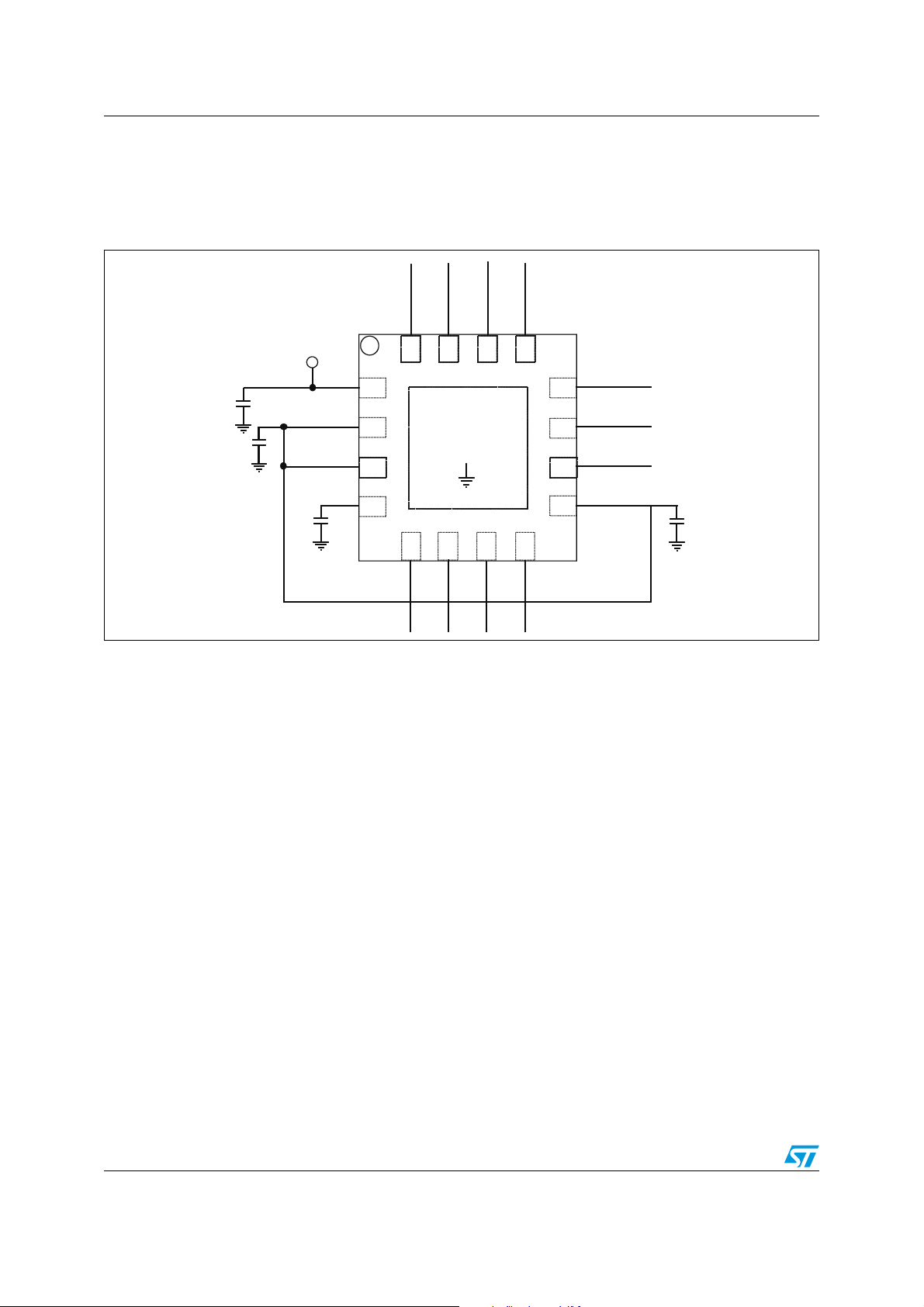
Theory of operation STPMS2
supply inputs. A 1 µF capacitor should be connected between VDDxx and GND. The input of
the regulator is VCC, which also powers the band-gap and bias generators. The band-gap
output is VBG, which should be connected to GND via a 100 nF capacitor.
Figure 16. Power supply external connection scheme
Analog Supply
3.3 - 5.0 V
DATn
DAT
CLK
MS3
MS2
MS1
MS0
VDDav
VIP
1 µF
1 µF
100 nF
VCC
VDDac
VDDa
VBG
GND
CIP
CIN
VIN
The analog part of the STPMS2 consists of:
● pre-amplifier in the current channel
● 1.23 V reference voltage generator (STPMS2L only)
● +3 V low-drop supply voltage regulator
● two sigma-delta 2
● BIST DAC
● AGND and V
● bias current generators
nd
order modulators
reference buffers
REF
1 µF
AM09381v1
The voltage channel has a pre-amplification gain of 2, which defines the maximum
differential voltage on voltage channel inputs to ± 300 mV. The relative gain of the current
channel is selectable among 2, 4, 8 or 16, which defines the maximum differential voltage on
the current channel to ± 300 mV, ± 150 mV, ± 75 mV or ± 37.5 mV, respectively. The full
range of gains is available only in soft mode (see Section 8.5), while in hard mode only 2
and 16 are selectable.
The temperature-compensated reference voltage generator produces V
generator is implemented as a band gap generator, whose temperature compensation
curve can be selected through configuration.
The low drop regulator fixes and stabilizes the core supply voltage to VDDa = 3 V. All digital
pads tolerate 5 V logic levels.
The STPMS2 is clocked by an external clock signal connected to pin CLK.
The STPMS2L sigma-delta modulators work in several operating modes, shown in Ta bl e 7
below.
18/33 Doc ID 16525 Rev 3
= 1.23 V. This
REF
Page 19
STPMS2 Theory of operation
Table 7. Operating modes
Operating mode Device f
LP (low power) LPR (low precision) STPMS2L 1 MHZ 1,2 mA typ
HP (fast)
LPR (low precision): f
HPR (high precision) STPMS2L 2 MHz – 4MHz
HHPR (very high precision) STPMS2H 4 MHz
= 1 MHz and settings defined by MS0 through MS3
CLK
HPR (high precision): the normal mode of operation with f
CLK
= 2 MHz to 4 MHz
CLK
Current
consumption
4 mA typ
The STPMS2H sigma-delta modulators work in the following mode:
HHPR (very high precision) external reference must be connected to VBG, f
CLK
= 4 MHz.
The STPMS2 performs operations in 2 basic modes: Hard mode and Soft mode.
In Hard mode the configuration is set through external pins MS0, MS1, MS2 and MS3.
In Soft mode, 40 configuration bits can be accessed through CFG[39:0], via serial
communication. The pins used for serial communication are: MS0, MS1 and MS2.
Switching between Hard and Soft modes is achieved through pin MS3.
● Hard mode: In this case the device configuration is bootstrapped at startup and signals
come from VIN and VIP for voltage channels, and CIP and CIN for current channels or
from internal BIST DAC.
● Soft mode: In this mode all possible settings from Hard mode are accessible, as well
as the additional settings described in Section 8.5.
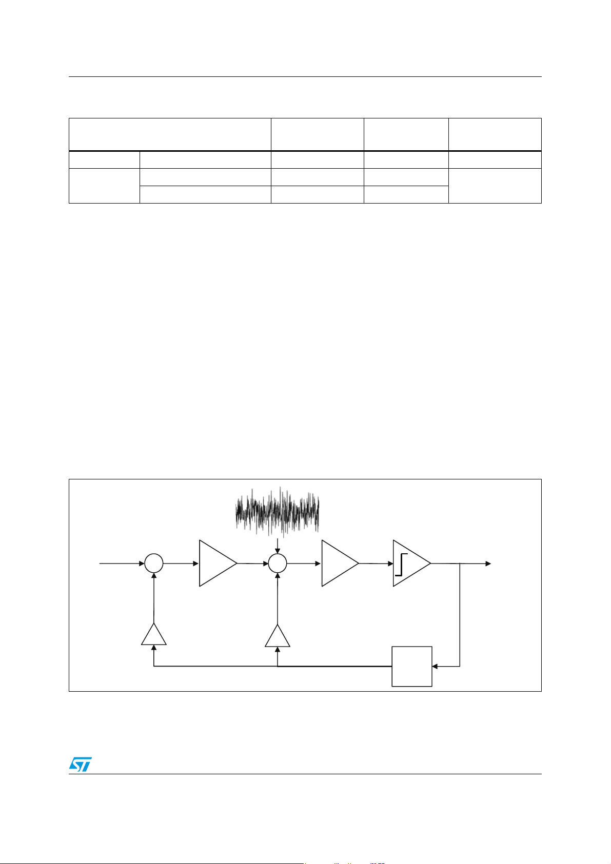
Figure 17. Block diagram of the modulator
dithering
input stream out
-
a
1
∫
st
1
integrator 2ndintegrator comparator
-
a
2
∫
D/A
The STPMS2 sends to the DAT and DATn pins selected signals based on the configuration
used.
Both outputs have cross-current and slew rate limiters to prevent excessive current spikes
on supply lines.
Doc ID 16525 Rev 3 19/33
AM09894v1
Page 20
Theory of operation STPMS2
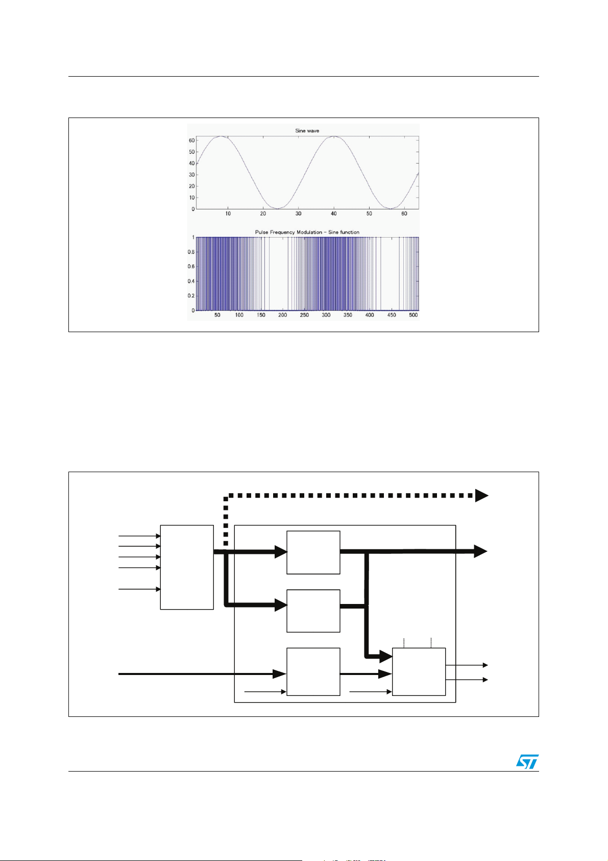
Figure 18. Example of sigma-delta modulator output in case of sinusoidal waveform
AM09895v1
8.3 Functional description of the digital part
The digital section (DFE) includes:
● a decoder for different modes of operation
● a generator for clock frequency
● level shifters, pull-up stages and power buffers outside the DFE block
Figure 19. Block diagram and definition of DFE digital signals
Outputs for analog part
Clock Generator
MS0
MS1
MS2
MS3
DECODER
CLK
Sigma-Delta streams
Chopper
Pseudo
Random
Synchro Mux
CLK CLK
Clock signals
DOMU L
DTMC
DAT
DATn
20/33 Doc ID 16525 Rev 3
AM09896v1
Page 21

STPMS2 Theory of operation
8.3.1 Decoder for different modes of operation
The decoder defines the operating mode according to the state of the bootstrap MS0, MS1,
MS2 and MS3 pins. Two different operational modes can be defined:
● Hard mode: In this case the device configuration is bootstrapped at startup and signals
come from VIN and VIP for voltage channels, and CIP and CIN for current channels or
from internal BIST DAC.
● Soft mode: In this mode all possible settings from Hard mode are accessible, as well as
additional settings such as dither and chopper signal frequencies and operation (see
Section 8.5).
8.3.2 Generator for clock frequency
Chopper and BIST frequency generator
The Chopper block generates the chopper frequencies and BIST signals for the voltage and
current channels. The BIST DAC output levels are appropriately adjusted for the current
channel according to the gain selection, while for the voltage channel the max DC voltage is
used.
The levels are 300 mV for the voltage channel and 300 mV / 150 mV / 75 mV / 37.5 mV for
the current channel, in accordance with gain settings 2/4/8/16, respectively, when operating
in Soft mode, while 300 mV / 37.5 mV based on gain settings 2/16 when operating in Hard
mode.
Pseudo random
The Pseudo random block generates pseudo random signals for the voltage and current
channels. These random signals are used to implement a dithering technique to decorrelate the output of the modulators and avoid accumulation points on the frequency
spectrum.
Synchro
In Synchro block the synchronization of sigma-delta input streams with strobe signals from
analog part and clock signal is performed.
Mux
In the Mux block, which signals are connected to output pins DAT and DATn are selected.
In HardMode, the output signals are selected by input pin MS2.
In SoftMode, the output signals are selected by 8 configuration bits.
8.4 Hard mode
The STPMS2 operates in Hard mode when input pin MS3 is connected to GND or VCC, as
described in Ta b le 1 1 .
In Hard mode, the STPMS2 has four digital input pins (MS0, MS1, MS2 and MS3) to
configure the basic operating parameters:
● BIST DAC enable
● temperature curve of reference voltage
● current and voltage channels settings
● output mode settings
Doc ID 16525 Rev 3 21/33
Page 22
Theory of operation STPMS2
In this way it is possible to access 128 different combinations, which are controlled through
pins MS0, MS1, MS2 and MS3.
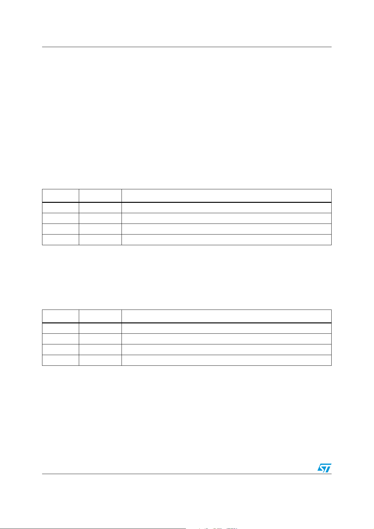
MS0 sets the operating mode and amplifier gain selection as described in Ta bl e 8 .
For the STPMS2L:
● MS0=GND or CLK to select LPR (low precision); f
= 1 MHz is the typical input clock
CLK
frequency and low power mode is selected.
● MS0=NCLK or VCC to select HPR (high precision): f
= 2 MHz is the typical input
CLK
clock frequency and accuracy is enhanced.
For the STPMS2H, LPR mode is not used and the settings should be chosen between
MS0=NCLK or VCC. In this case, f
= 4 MHz is typical.
CLK
The relative gain of the current channel is selectable between 2 or 16, which defines the
maximum differential voltage on the current channel to ± 300 mV or ± 37.5 mV, respectively.
The voltage channel gain setting is fixed at 2, which defines the maximum differential
voltage on the voltage channel inputs to ± 300 mV.
Table 8. Precision mode and input amplifier gain selection
MS0 Mode Description
GND 0 LPR, amplifier GAIN selection g3 = 16
CLK 1 LPR, amplifier GAIN selection g0 = 2
NCLK 2 HPR, amplifier GAIN selection g0 = 2
VCC 3 HPR, amplifier GAIN selection g3 = 16
MS1 defines the temperature compensation (TC) curve of the internal voltage reference of
the STPMS2L, as described in Ta bl e 9 . This bootstrap function is not used with the
STPMS2H. The temperature-compensated reference voltage generator produces V
1.23 V. This generator is implemented as a band gap generator, whose temperature
compensation curve can be selected through the MS1 configuration pin.
Table 9. TC of the band-gap reference
MS1 Mode Description
GND 0 TC = 60 ppm/°C
CLK 1 Flattest TC = +30 ppm/°C
NCLK 2 TC = +160 ppm/°C
VCC 3 TC = -160 ppm/°C
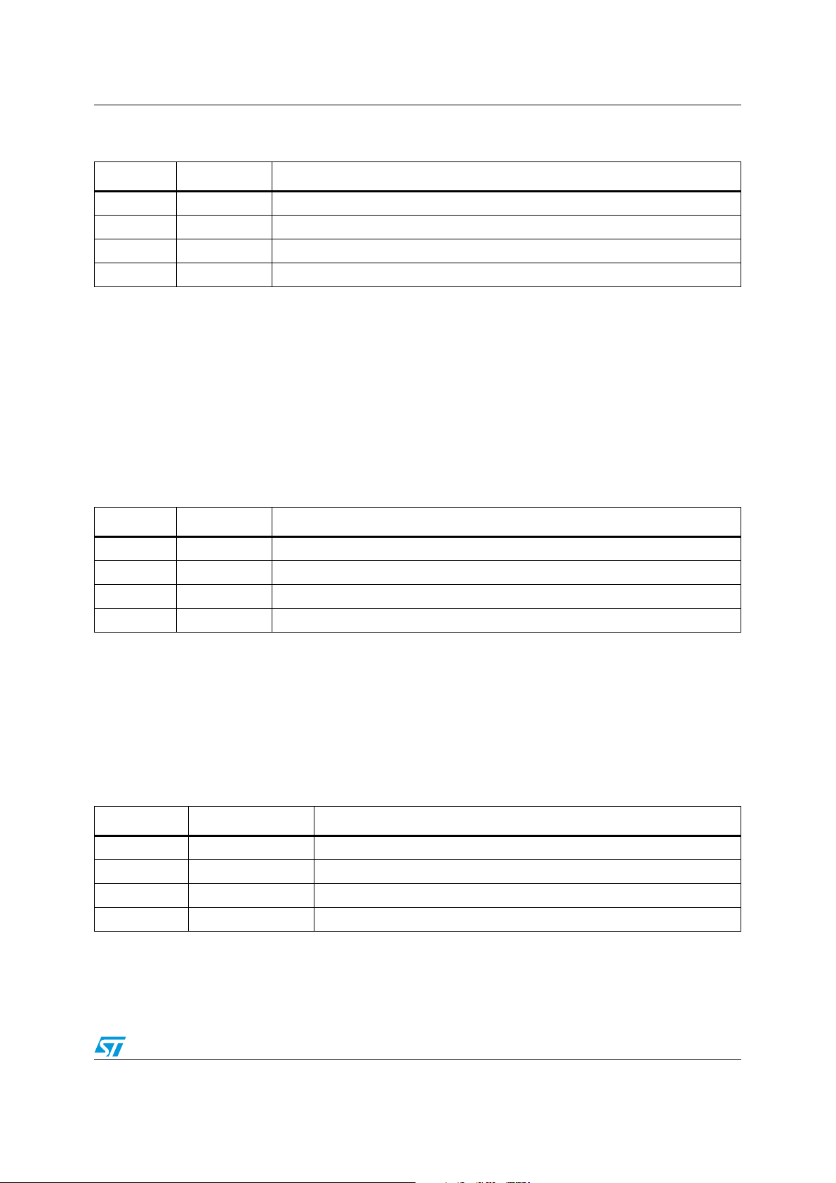
MS2 defines the outputs of the device:
The STPMS2 sends to the DAT and DATn pins the sigma-delta streams synchronous to the
CLK signal. The output mode can be configured according to Tab l e 1 0 as follows:
● The output current channel's sigma-delta stream on DAT and the voltage channel's
sigma-delta stream on DATn
● Output multiplexed signals, so when CLK = 0, the current channel output sigma-delta
value is set on the DAT pin, and when CLK = 1, the voltage channel output sigma-delta
value is set on the DAT pin. The DATn pin tracks DAT, so DATn = ~DAT.
● Output current channel's sigma-delta stream on DAT and the current channel's sigma-
delta stream negated on DATn
REF
=
22/33 Doc ID 16525 Rev 3
Page 23
STPMS2 Theory of operation
Table 10. Control of voltage channel and output signals
MS2 Mode Description
GND 0 Voltage channel ON, DATn = ~ [DAT =(CLK) ? bsV : bsC)]
CLK 1 Voltage channel OFF, DATn = bsCn, DAT = bsC
NCLK 2 Voltage channel OFF, DATn = bsCn, DAT = bsC
VCC 3 Voltage channel ON, DATn = bsC, DAT = bsV
MS3 enables or disables the BIST DAC output levels.
If enabled (MS3=VCC), the input of the modulators are disconnected from pin VIP, VIN and
CIP, and CIN, and connected to the output of BIST DAC which generates 2 different levels
appropriately adjusted for the current channel 300 mV / 37.5 mV depending on gain settings
2/16, while for the voltage channel, 300 mV is used. This mode is used as auto diagnostic
methodology of good behavior of the two modulators.
When disabled (MS3=GND), the input of the modulators comes from pins VIP, VIN and CIP,
and CIN. This is the normal operating condition.
Table 11. Selection of Hard, Soft or Test mode and enable of BIST
MS3 Mode Description
GND 0 HardMode, BIST mode OFF
CLK 1 Soft mode
NCLK 2 Reserved
VCC 3 HardMode, BIST mode ON
8.5 Soft mode
The STPMS2 switches to Soft mode when MS3 is connected to CLK. In Soft mode, input
pins MS0, MS1 and MS2 control the serial communication port, as described in Ta bl e 1 2.
This way, all settings of the 40 internal configuration bits can be changed. The old values
remain in the registers until they are overwritten.
Table 12. Pins for SPI communication
Pin Function Description
MS0 SCL Clock input
MS1 TDI Data input
MS2 TDS Enable
MS3 CLK SPI operation
Doc ID 16525 Rev 3 23/33
Page 24

Theory of operation STPMS2
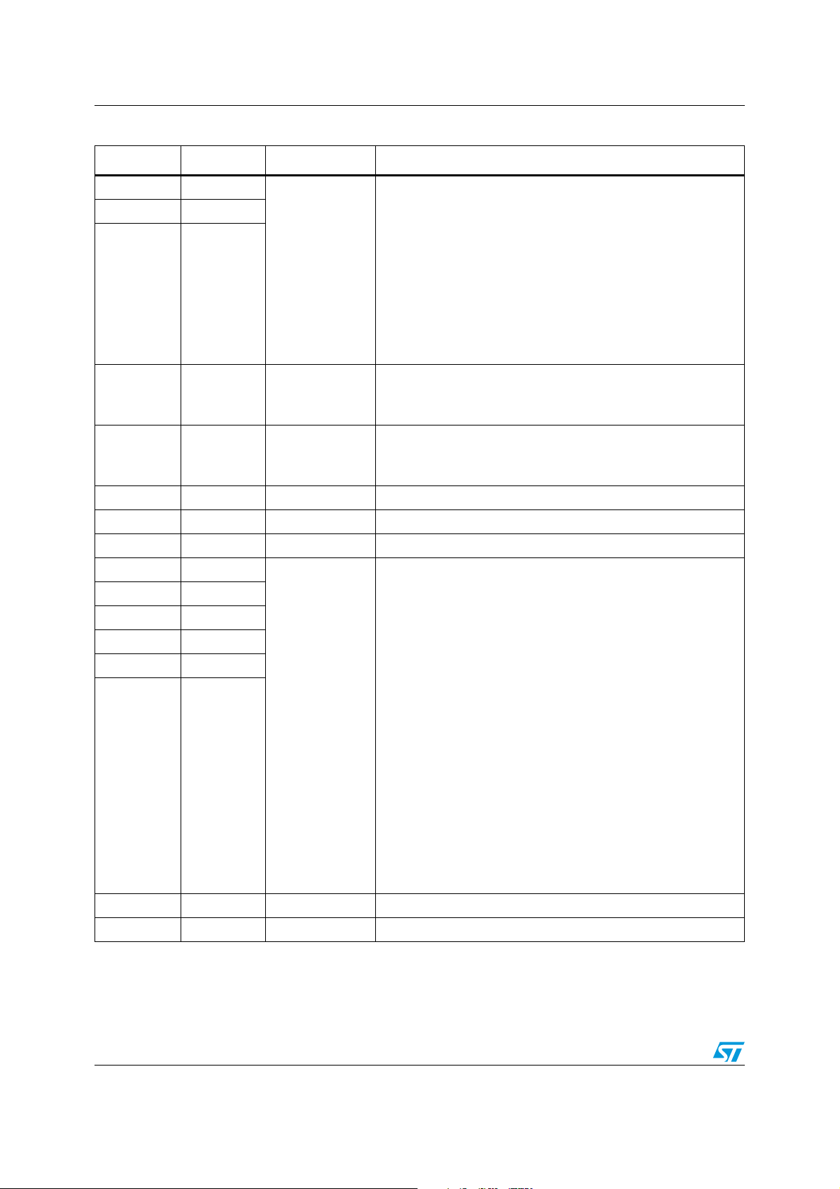
Table 13. Description of output signals and configuration bits CFG[39:0]
Hard mode Soft mode Internal signal Description
Operating mode:
MS0 CFG[0] LP/HP
MS0 CFG[1]
GAIN
MS0 CFG[2]
MS1 CFG[3]
TC
MS1 CFG[4]
MS2 CFG[5] DOMUL
MS2 CFG[6] PDV
LP/HP=0: LPR
LP/HP=1: HPR
Gain selector of current channel pre-amplifier:
GAIN=0: x2
GAIN=1: x4
GAIN=2: x8
GAIN=3: x16
Temperature compensation of voltage reference:
TC=0: TC = 60 ppm/°C
TC=1: Flattest TC = +30 ppm/°C
TC=2: TC = +160 ppm/°C
TC=3: TC = -160 ppm/°C
Output multiplexer enable:
DOMUL=0: outputs not multiplexed
DOMUL=1: outputs multiplexed
Power-down of voltage modulator:
PDV=0: Voltage modulator on
PDV=1: Voltage modulator off
MS3 CFG[7] EBISTC
MS3 CFG[8] EBISTV
MS3 CFG[9] EINCHPC
MS3 CFG[10] EINCHPV
1 CFG[11] ECHPLFC
Current modulator BIST DAC enable:
EBISTC=0: BISTC disabled
EBISTC=1: BISTC enabled
– EBISTC Frequency output
0 0
15
1 CLK/2
x LFC
Voltage modulator BIST DAC enable:
EBISTC=0: BISTV disabled
EBISTC=1: BISTV enabled
– EBISTV Frequency output
0 0
15
1 CLK/2
x LFV
CIP, CIN input pin enable:
EINCHPC=0: CIN CIP disabled
EINCHPC=1: CIN CIP enabled
VIP, VIN input pin enable:
EINCHPC=0: VIN VIP disabled
EINCHPC=1: VIN VIP enabled
Low frequency chopper of current modulator enable:
ECHPLFC=0: LFC disabled
ECHPLFC=1: LFC enabled
(1)
24/33 Doc ID 16525 Rev 3
Page 25

STPMS2 Theory of operation
Table 13. Description of output signals and configuration bits CFG[39:0] (continued)
Hard mode Soft mode Internal signal Description
1CFG[12]
0CFG[13]
LFC of current channel frequency selector:
– MC[2:0] Frequency
000 CLK/1024
001
MC
0CFG[14]
010 CLK/256
011 CLK/128
100 CLK/64
101
110
111
High Frequency Chopper of current modulator enable:
1 CFG[15] ECHPHFC
ECHPHFC=0: HFC disabled
ECHPHFC=1: HFC enabled
1CFG[16]
1CFG[17]
HFC of current channel frequency selector
– NC[2:0] Frequency
000
001
NC
0CFG[18]
010 CLK/256
011
100 CLK/64
101 CLK/32
110 CLK/16
111 CLK/8
Low Frequency Chopper of voltage modulator enable:
1CFG[19]ECHPLFV
ECHPLFV=0: LFV disabled
ECHPLFV=1: LFV enabled
(1)
CLK/512
(2)
CLK/64
(2)
CLK/64
(2)
CLK/64
(2)
CLK/256
(2)
CLK/128
(1)
CLK/128
(1)
(1)
1CFG[20]
0CFG[21]
MV
0CFG[22]
1 CFG[23] ECHPHFV
LFC of voltage channel frequency selector:
– MV[2:0] Frequency
000 CLK/1024
(1)
001
CLK/512
010 CLK/256
011 CLK/128
100 CLK/64
(2)
101
110
111
CLK/64
(2)
CLK/64
(2)
CLK/64
High Frequency Chopper of voltage modulator enable:
ECHPHFC=0: HFV disabled
ECHPHFC=1: HFV enabled
(1)
Doc ID 16525 Rev 3 25/33
Page 26
Theory of operation STPMS2
Table 13. Description of output signals and configuration bits CFG[39:0] (continued)
Hard Mode Soft mode Internal signal Description
1CFG[24]
1CFG[25]
HFC of voltage channel frequency selector:
– NV[2:0] Frequency
000
001
NV
0CFG[26]
010 CLK/256
011
(1)
100 CLK/64
101 CLK/32
110 CLK/16
111 CLK/8
Current modulator pseudo random signals enable:
1 CFG[27] EPRSC
EPRSC=0: PRSC disabled
EPRSC=1: PRSC enabled
Voltage modulator pseudo random signals enable:
1 CFG[28] EPRSV
EPRSV=0: PRSV disabled
EPRSV=1: PRSV enabled
0 CFG[29] - Reserved
0 CFG[30] - Reserved
0 CFG[31] - Reserved
0CFG[32]
0CFG[33]
0CFG[34]
0CFG[35]
0CFG[36]
DAT and DAT output signal selector:
– DTMC[5:0] pdV domul DAT DATn
00XXXX 0 0 bsV bsC
00XXXX 0 1 (bsV,bsC) (bsVn,bsCn)
00XXXX 1 0 bsC bsCn
00XXXX 1 1 bsC bsCn
01XX00 0 0 bsV LFC
01XX01 0 1 (bsV,bsC) HFC
DTMC
01XX10 1 0 bsC BISTC
01XX11 1 1 bsC PRSC
1000XX 0 0 LFV bsC
1001XX 0 1 HFV (bsVn,bsCn)
0CFG[37]
1010XX 1 0 BISTV bsCn
1011XX 1 1 PRSV bsCn
110000 X X LFV LFC
110101 X X HFV HFC
111010 X X BISTV BISTC
111111 X X PRSV PRSC
0 CFG[38] - Reserved
0 CFG[39] - Reserved
(2)
CLK/256
(2)
CLK/128
CLK/128
(1)
(1)
1. Default value for Hard mode
2. Combinations not used
26/33 Doc ID 16525 Rev 3
Page 27
STPMS2 Theory of operation
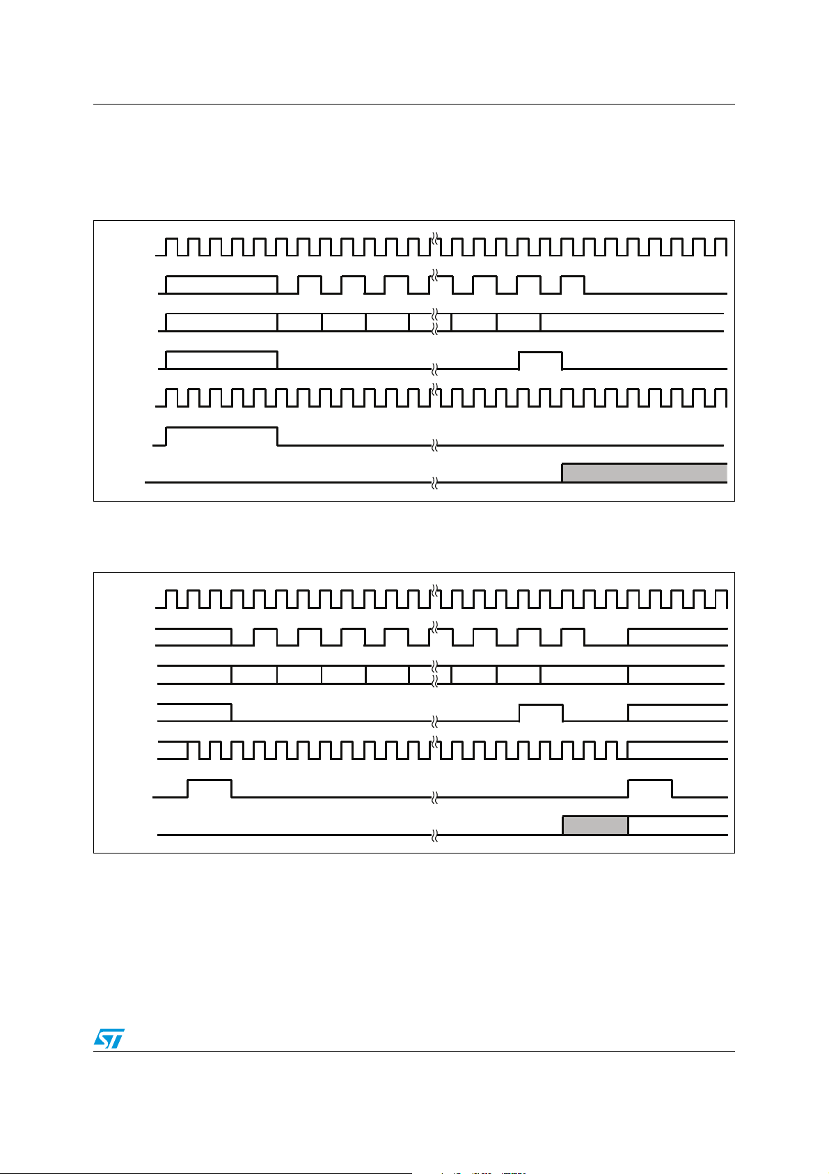
8.5.1 Writing to the configuration register in Soft mode
All 40 configuration bits must be overwritten.
Figure 20. Timings to switch to Soft mode after POR
CLK
MS0/SCL
MS1/TDI
CFG[0] CFG[1] CFG[2] CFG[38]
MS2/TDS
MS3/CLK
1
delay
CFG
1. After power-on reset, Soft mode is selected (MS3=CLK), the bits MS0 .. MS2 must be stable at least 5*CLK
Figure 21. Timings to switch to Soft mode
CLK
MS0/SCL
MS1/TDI
CFG[0]
CFG[1] CFG[2] CFG[3] CFG[38]
MS2/TDS
CFG[39]
NEW v alues
AM09897v1
CFG[39]
MS3/CLK
2
delay
CFG
OLD values Hard Mode
2. After switching into Soft mode (MS3=CLK), the bits MS0 .. MS2 must be stable at least 2*CLK. The same
rule applies when switching from Soft mode to Hard mode: MS0 .. MS2 must be stable at least 2*CLK
NEW v alues
AM09898v1
Doc ID 16525 Rev 3 27/33
Page 28
Package mechanical data STPMS2
9 Package mechanical data
In order to meet environmental requirements, ST offers these devices in different grades of
ECOPACK
specifications, grade definitions and product status are available at: www.st.com.
ECOPACK
®
packages, depending on their level of environmental compliance. ECOPACK®
®
is an ST trademark.
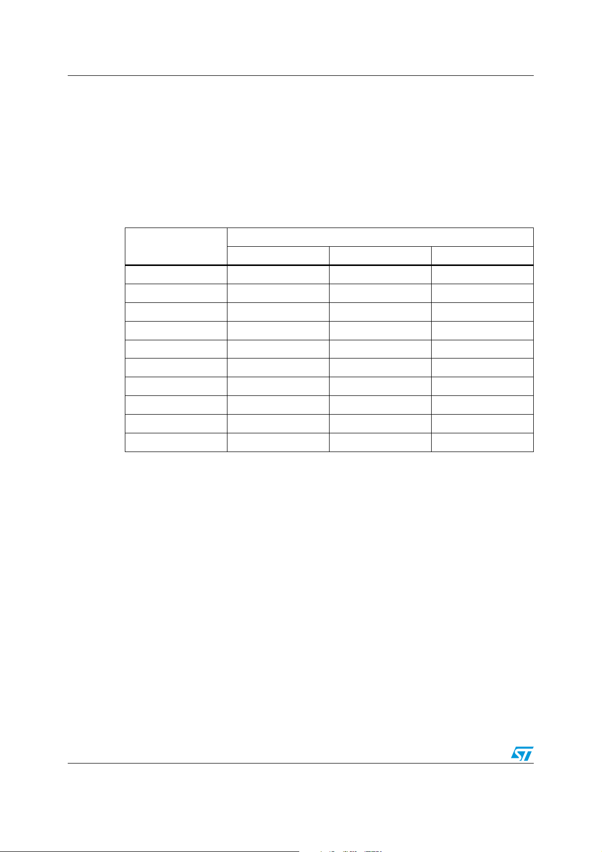
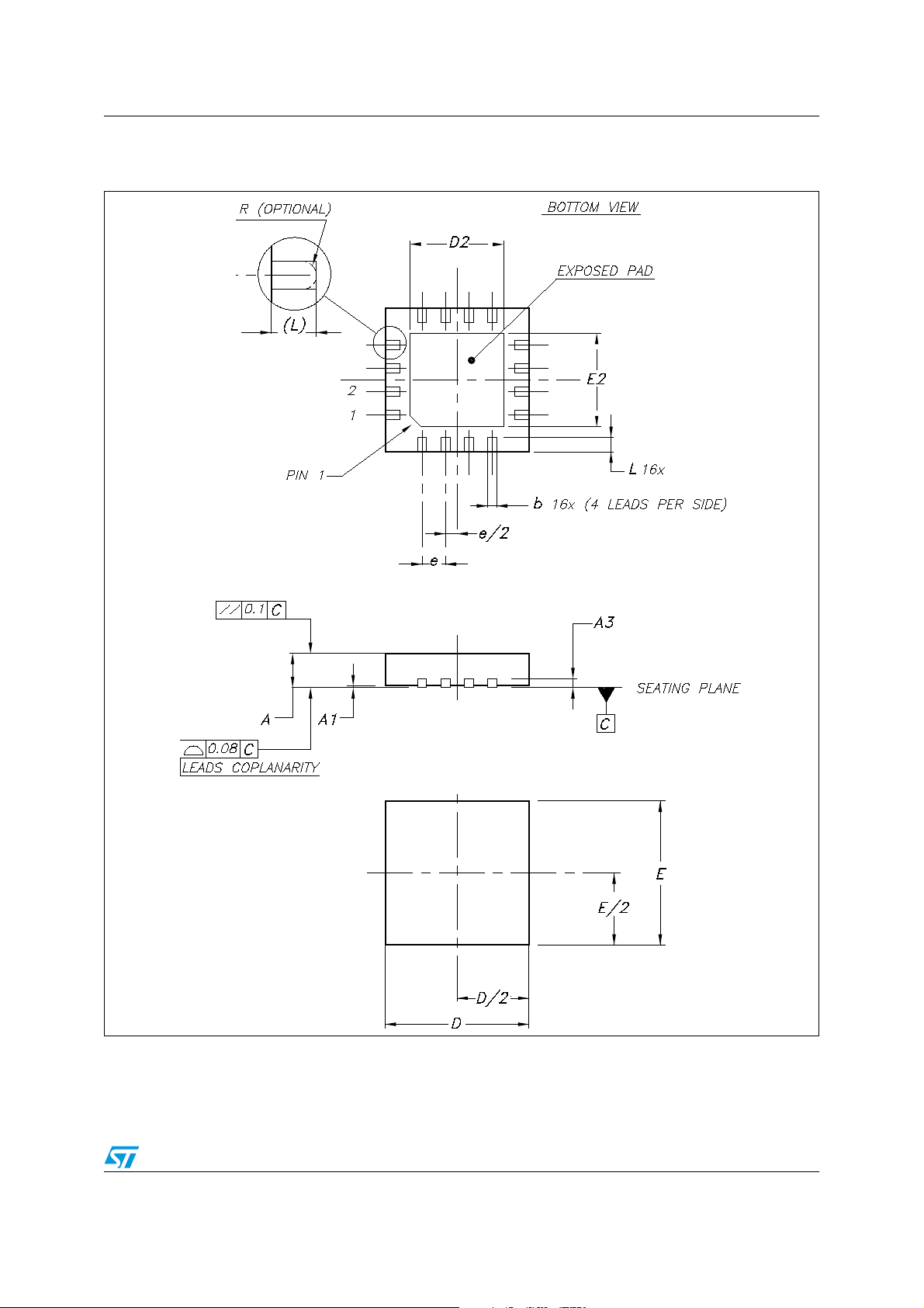
Table 14. QFN16 (4 x 4 mm.) mechanical data
Dim.
Min. Typ. Max.
A 0.80 0.90 1.00
A1 0.00 0.02 0.05
A3 0.20
b 0.25 0.30 0.35
D 3.90 4.00 4.10
D2 2.50 2.80
E 3.90 4.00 4.10
E2 2.50 2.80
e0.65
mm.
L 0.30 0.40 0.50
28/33 Doc ID 16525 Rev 3
Page 29
STPMS2 Package mechanical data
Figure 22. QFN16 (4 x 4 mm.) drawing
7571203_A
Doc ID 16525 Rev 3 29/33
Page 30
Package mechanical data STPMS2
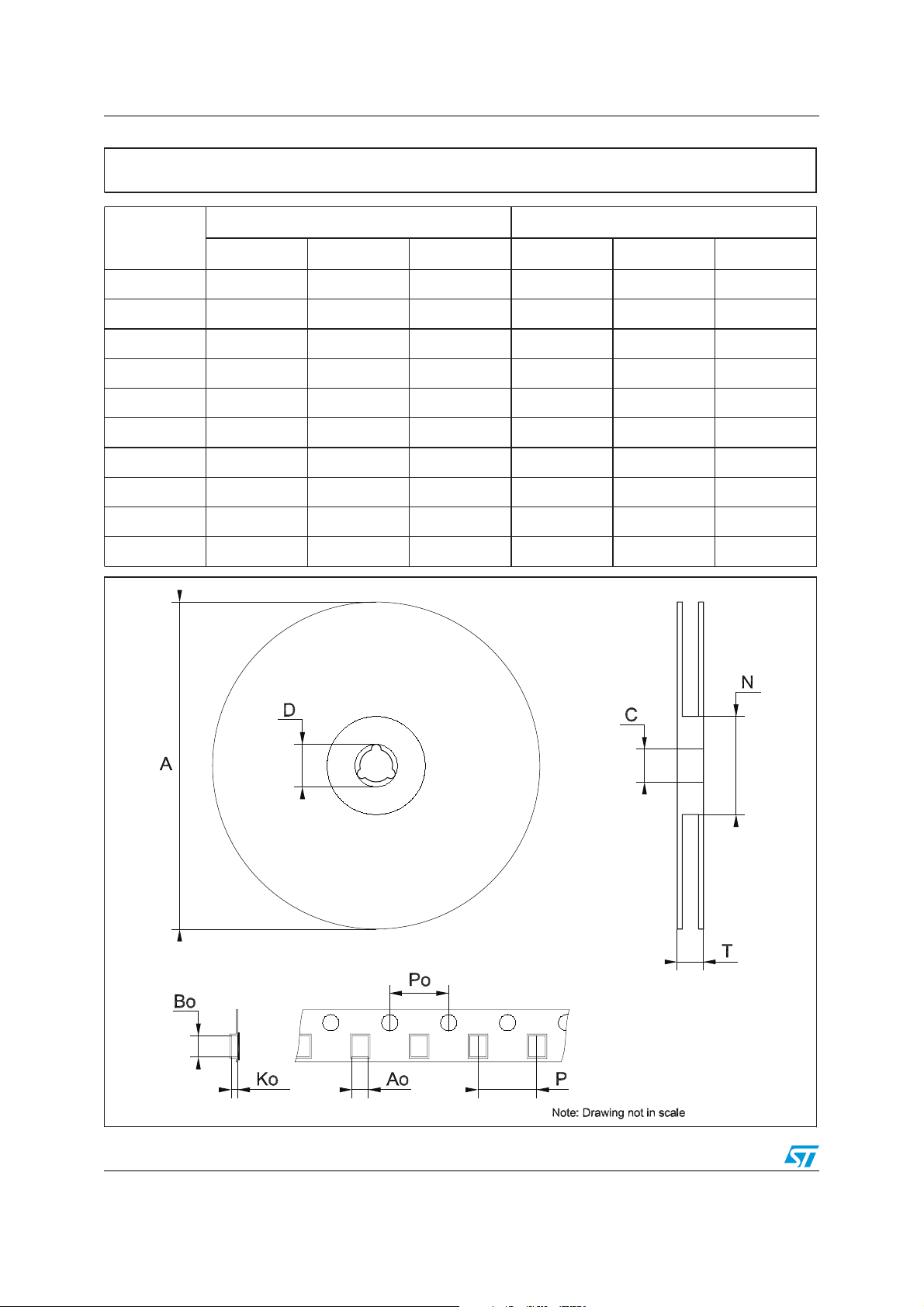
Tape & reel QFNxx/DFNxx (4x4) mechanical data
mm. inch.
Dim.
Min. Typ. Max. Min. Typ. Max.
A 330 12.992
C 12.8 13.2 0.504 0.519
D 20.2 0.795
N 99 101 3.898 3.976
T 14.4 0.567
Ao 4.35 0.171
Bo 4.35 0.171
Ko 1.1 0.043
Po 4 0.157
P 8 0.315
30/33 Doc ID 16525 Rev 3
Page 31
STPMS2 Package mechanical data
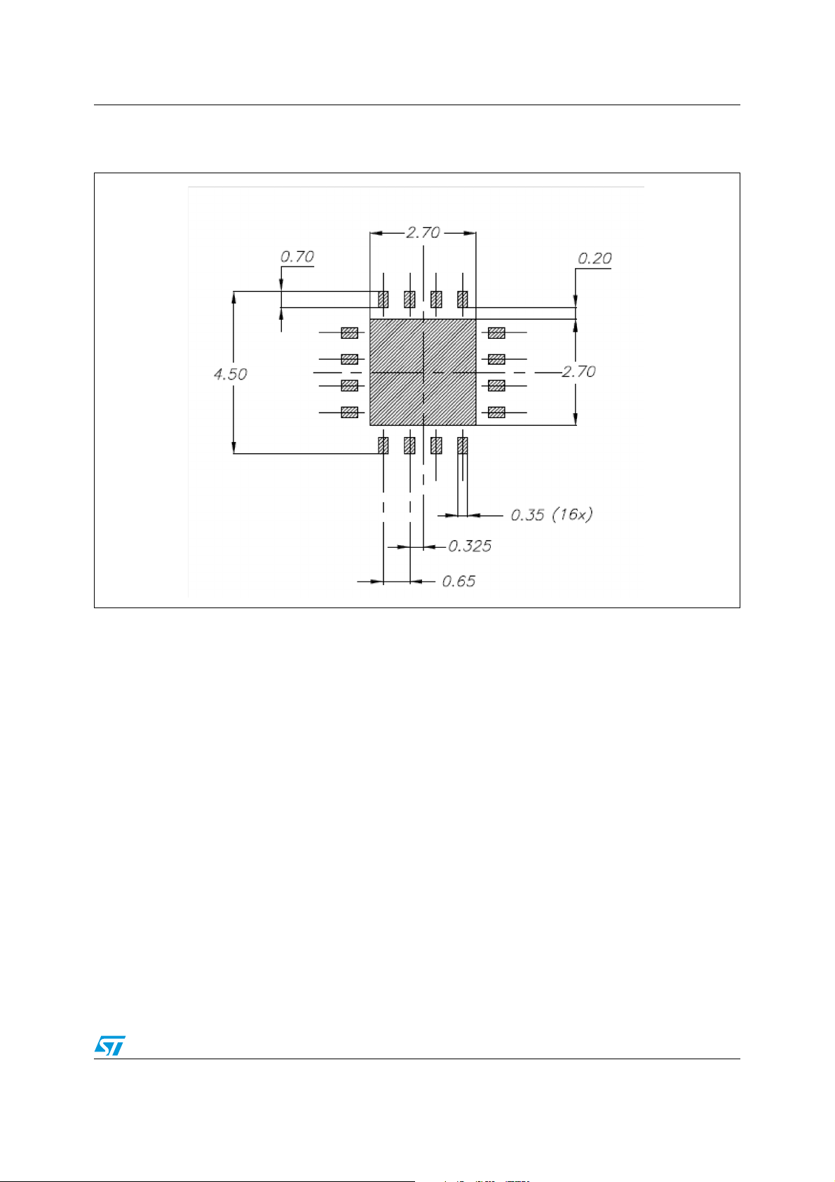
Figure 23. QFN16 (4 x 4) footprint recommended data (dimension in mm.)
Doc ID 16525 Rev 3 31/33
Page 32

Revision history STPMS2
10 Revision history
Table 15. Document revision history
Date Revision Changes
23-Oct-2009 1 Initial release.
06-Jul-2011 2 Document status promoted from preliminary data to datasheet.
11-Oct-2011 3 Modified: 100 µF ==> 100 nF Section 8.2 on page 17.
32/33 Doc ID 16525 Rev 3
Page 33

STPMS2
Please Read Carefully:
Information in this document is provided solely in connection with ST products. STMicroelectronics NV and its subsidiaries (“ST”) reserve the
right to make changes, corrections, modifications or improvements, to this document, and the products and services described herein at any
time, without notice.
All ST products are sold pursuant to ST’s terms and conditions of sale.
Purchasers are solely responsible for the choice, selection and use of the ST products and services described herein, and ST assumes no
liability whatsoever relating to the choice, selection or use of the ST products and services described herein.
No license, express or implied, by estoppel or otherwise, to any intellectual property rights is granted under this document. If any part of this
document refers to any third party products or services it shall not be deemed a license grant by ST for the use of such third party products
or services, or any intellectual property contained therein or considered as a warranty covering the use in any manner whatsoever of such
third party products or services or any intellectual property contained therein.
UNLESS OTHERWISE SET FORTH IN ST’S TERMS AND CONDITIONS OF SALE ST DISCLAIMS ANY EXPRESS OR IMPLIED
WARRANTY WITH RESPECT TO THE USE AND/OR SALE OF ST PRODUCTS INCLUDING WITHOUT LIMITATION IMPLIED
WARRANTIES OF MERCHANTABILITY, FITNESS FOR A PARTICULAR PURPOSE (AND THEIR EQUIVALENTS UNDER THE LAWS
OF ANY JURISDICTION), OR INFRINGEMENT OF ANY PATENT, COPYRIGHT OR OTHER INTELLECTUAL PROPERTY RIGHT.
UNLESS EXPRESSLY APPROVED IN WRITING BY TWO AUTHORIZED ST REPRESENTATIVES, ST PRODUCTS ARE NOT
RECOMMENDED, AUTHORIZED OR WARRANTED FOR USE IN MILITARY, AIR CRAFT, SPACE, LIFE SAVING, OR LIFE SUSTAINING
APPLICATIONS, NOR IN PRODUCTS OR SYSTEMS WHERE FAILURE OR MALFUNCTION MAY RESULT IN PERSONAL INJURY,
DEATH, OR SEVERE PROPERTY OR ENVIRONMENTAL DAMAGE. ST PRODUCTS WHICH ARE NOT SPECIFIED AS "AUTOMOTIVE
GRADE" MAY ONLY BE USED IN AUTOMOTIVE APPLICATIONS AT USER’S OWN RISK.
Resale of ST products with provisions different from the statements and/or technical features set forth in this document shall immediately void
any warranty granted by ST for the ST product or service described herein and shall not create or extend in any manner whatsoever, any
liability of ST.
ST and the ST logo are trademarks or registered trademarks of ST in various countries.
Information in this document supersedes and replaces all information previously supplied.
The ST logo is a registered trademark of STMicroelectronics. All other names are the property of their respective owners.
© 2011 STMicroelectronics - All rights reserved
STMicroelectronics group of companies
Australia - Belgium - Brazil - Canada - China - Czech Republic - Finland - France - Germany - Hong Kong - India - Israel - Italy - Japan -
Malaysia - Malta - Morocco - Philippines - Singapore - Spain - Sweden - Switzerland - United Kingdom - United States of America
www.st.com
Doc ID 16525 Rev 3 33/33
 Loading...