

Page 1

Features
STPMS1
Dual-channel 1-bit, 2 MHz, 1st order
sigma-delta modulator with embedded PGA
■ V
■ Two 1
■ Programmable chopper-stabilized low noise
supply range: 3.2 V - 5.5 V
CC
st
order sigma-delta modulators
and low offset amplifier
■ Supports 50-60 Hz AC watt meters
■ Internal low-drop regulator at 3 V (typ.)
■ Precision voltage reference: 1.23 V and 30
ppm/°C (typ.)
Applications
■ Power metering
■ Motor control
■ Industrial process control
■ Weight scale
■ Pressure transducers
Description
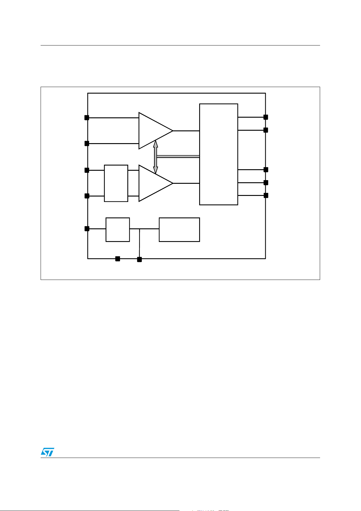
The STPMS1, also called a smart-sensor device,
is an ASSP designed for effective measurement
in power line systems utilizing the Rogowski coil,
current transformer, or shunt principle. It is used
in combination with the STPMC1 programmable
poly-phase energy calculator IC, as a building
block for single-phase or poly-phase energy
meters. The STPMS1 is a mixed signal IC
consisting of an analog and a digital section. The
analog section consists of a pre-amplifier and two
st
1
order ΣΔ modulator blocks, band-gap voltage
reference, a low-drop voltage regulator, and DC
buffers, while the digital section consists of a clock
generator and output multiplexer. This device is
designed for use in medium resolution
Table 1. Device summary
QFN16 (3 x 3 mm.)
measurement applications when single or double
inputs must be monitored at the same time.
Order code Package Packaging
STPMS1BPQR QFN16 (3 x 3 mm) 2500 parts per reel
October 2010 Doc ID 16524 Rev 2 1/23
www.st.com
23
Page 2

Contents STPMS1
Contents
1 Schematic diagram . . . . . . . . . . . . . . . . . . . . . . . . . . . . . . . . . . . . . . . . . . 3
2 Pin configuration . . . . . . . . . . . . . . . . . . . . . . . . . . . . . . . . . . . . . . . . . . . . 4
3 Electrical characteristics . . . . . . . . . . . . . . . . . . . . . . . . . . . . . . . . . . . . . 5
4 General operating conditions . . . . . . . . . . . . . . . . . . . . . . . . . . . . . . . . . 6
5 Application . . . . . . . . . . . . . . . . . . . . . . . . . . . . . . . . . . . . . . . . . . . . . . . . . 9
6 Terminology . . . . . . . . . . . . . . . . . . . . . . . . . . . . . . . . . . . . . . . . . . . . . . . 12
6.1 Conventions . . . . . . . . . . . . . . . . . . . . . . . . . . . . . . . . . . . . . . . . . . . . . . . 12
6.2 Notation . . . . . . . . . . . . . . . . . . . . . . . . . . . . . . . . . . . . . . . . . . . . . . . . . . 12
7 Typical performance characteristics . . . . . . . . . . . . . . . . . . . . . . . . . . . 13
8 Theory of operation . . . . . . . . . . . . . . . . . . . . . . . . . . . . . . . . . . . . . . . . 15
8.1 General operation description . . . . . . . . . . . . . . . . . . . . . . . . . . . . . . . . . 15
8.2 Function description of the analog part . . . . . . . . . . . . . . . . . . . . . . . . . . 15
8.3 Functional description of the digital part . . . . . . . . . . . . . . . . . . . . . . . . . . 17
9 Package mechanical data . . . . . . . . . . . . . . . . . . . . . . . . . . . . . . . . . . . . 18
10 Revision history . . . . . . . . . . . . . . . . . . . . . . . . . . . . . . . . . . . . . . . . . . . 22
2/23 Doc ID 16524 Rev 2
Page 3
STPMS1 Schematic diagram
1 Schematic diagram
Figure 1. Block diagram
DAT
VIP
VIP
VIN
VIN
CIP
CIP
CIN
CIN
PGA
PGA
8x, 32x
8x, 32x
1stord
1stord
modulator
modulator
1stord
1stord
modulator
modulator
ΣΔ
ΣΔ
ΣΔ
ΣΔ
DIGITAL
DIGITAL
FRONT
FRONT
END
END
DAT
DATN
DATN
MS1
MS1
MS0
MS0
CLK
CLK
VCC
VCC
LDO
LDO
BIAS
BIAS
Ref
Ref
AM07830v1
AM07830v1
VDDGND
VDDGND
Doc ID 16524 Rev 2 3/23
Page 4
Pin configuration STPMS1
2 Pin configuration
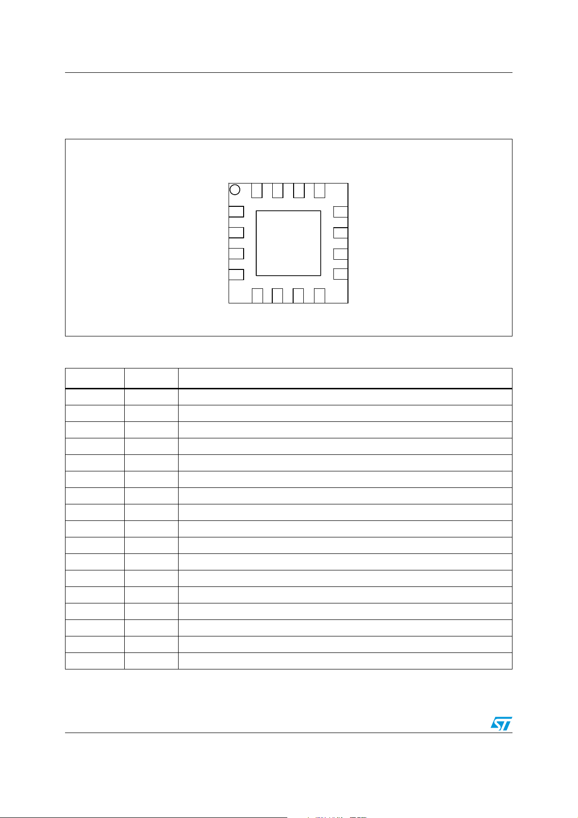
Figure 2. Pin connection (top view)
DAT
VDD
VDD
GND
GND
VDDac
VDDac
GND
GND
DAT
VCC
VCC
1
1
GND
GND
CIP
CIP
CIN
CIN
DATN
DATN
VIP
VIP
CLK
CLK
VIN
VIN
MS1
MS1
MS0
MS0
VDDd
VDDd
VDDav
VDDav
AM07831v1
AM07831v1
Table 2. Pin description
Pin Symbol Description
1 VDD + 3.0 V output of LDO
2 GND Ground level for signals and pin protection
3 VDDac Current channel modulator supply input
4 GND Ground level for signals and pin protection
5 CIP Current channel +
6 CIN Current channel -
7 VIP Voltage channel +
8 VIN Voltage channel -
9 VDDav Voltage channel modulator supply input
10 VDDd Digital front-end supply input
11 MS0 Input for configurator 0
12 MS1 Input for configurator 1
13 CLK Input for external measurement clock
14 DAT Output of multiplexed ΣΔ signal
15 DATn Output of multiplexed ΣΔ signal negated
16 VCC Unregulated supply voltage
Exp PAD GND Ground level for signals and pin protection
4/23 Doc ID 16524 Rev 2
Page 5
STPMS1 Electrical characteristics
3 Electrical characteristics
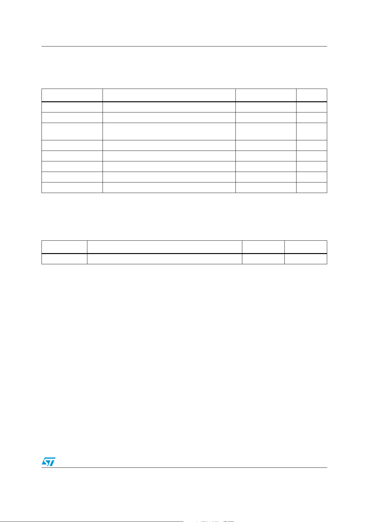
Table 3. Absolute maximum ratings
Symbol Parameter Value Unit
VCC DC input voltage -0.3 to 6 V
I
PIN
V
ID
V
IA
ESD Human body model (all pins) ±3.5 kV
T
OP
T
J
T
STG
Note: Absolute maximum ratings are those values beyond which damage to the device may occur.
Functional operation under these conditions is not implied.
Current on any pin (sink/source) ±150 mA
Input voltage at digital pins (MS0, MS1, CLK, DAT,
DATN)
-0.3 to V
+0.3 V
CC
Input voltage at analog pins (VIP, VIN, CIP, CIN) -0.7 to 0.7 V
Operating ambient temperature -40 to 85 °C
Junction temperature -40 to 150 °C
Storage temperature range -55 to 150 °C
Table 4. Thermal data
Symbol Parameter Value Unit
R
thJA
1. This value refers to a single-layer PCB, JEDEC standard test board.
Thermal resistance junction-ambient 38.10
(1)
°C/W
Doc ID 16524 Rev 2 5/23
Page 6
General operating conditions STPMS1
4 General operating conditions
VCC = 5 V, TA = 25 °C, 2.2 µF between VDD and GND, 100 nF between VCC and GND,
f
= 2.048 MHz unless otherwise specified.
CLK
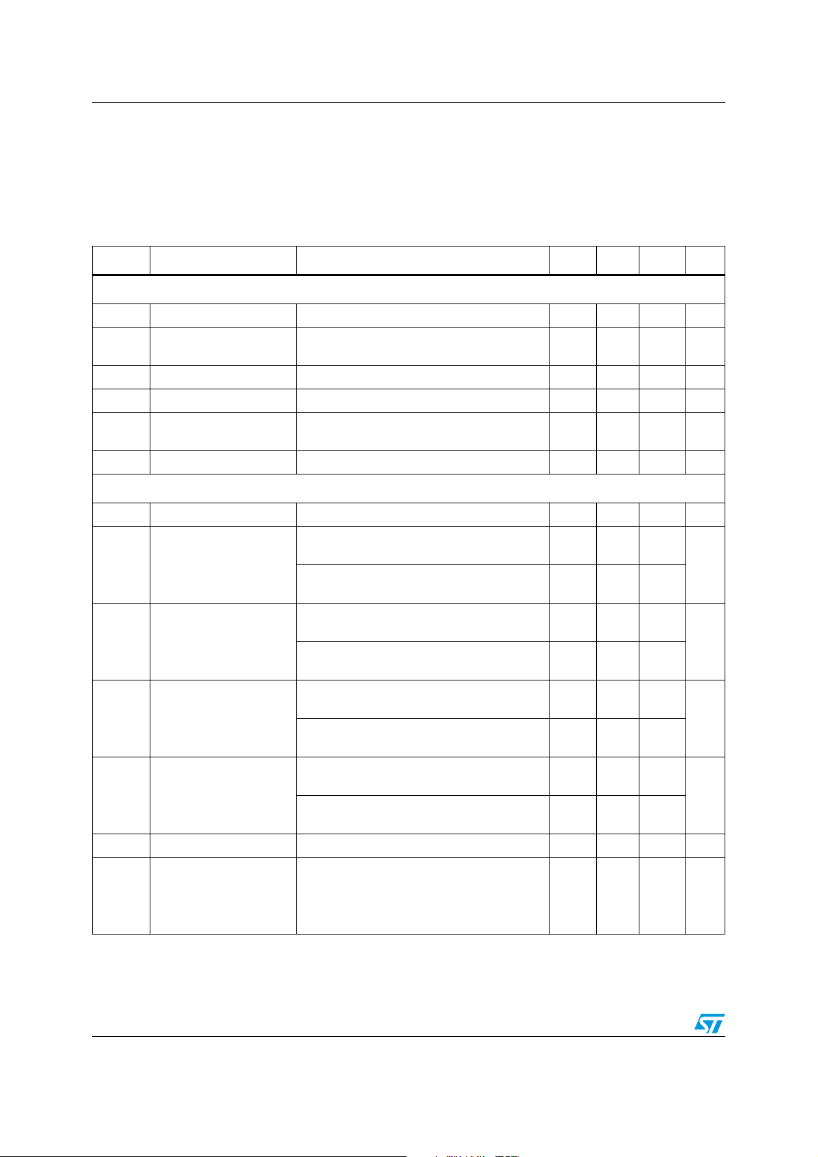
Table 5. General operating conditions
Symbol Parameter Test conditions Min. Typ. Max. Unit
General section
V
I
V
V
I
LATCH
f
Operating supply voltage 3.165 5.5 V
CC
Quiescent current
CC
Power on reset on V
POR
Regulated supply voltage 1.049 MHz; VCC=3.2 V; CL=100 nF, no loads 2.85 3.00 3.15 V
DD
Current injection latch-up
immunity
Nominal frequencies 1.0 2.458 MHz
CLK
DC measurement accuracy
Resolution 11 16 bit
INL Integral non-linearity
DNL Differential linearity
Offset error
Gain error
1.049 MHz; V
=3.165 V; CL=100 nF, no
CC
loads
CC
Result referred to a 13-bit resolution of CIPCIN channel
Result referred to a 9-bit resolution of VIPVIN channel
Result referred to a 13-bit resolution of CIPCIN channel
Result referred to a 9-bit resolution of VIPVIN channel
Result referred to a 13-bit resolution of CIPCIN channel
Result referred to a 9-bit resolution of VIPVIN channel
Result referred to a 13-bit resolution of CIPCIN channel
Result referred to a 9-bit resolution of VIPVIN channel
2.5 mA
2.5 V
300 mA
0.35
LSB
0.5
0.2
LSB
0.4
0.15
LSB
0.05
0.05
LSB/
µV
0.001
NF Noise floor CIP-CIN channel, Gain 8x 115 dB
rms
rms
/50 Hz
/50 Hz
0.2 %
PSRR
Power supply DC
DC
rejection
Voltage signal: 200 mV
Current signal: 10 mV
f
= 2.048 MHz
CLK
=3.3 V±10 %, 5 V±10 %
V
CC
6/23 Doc ID 16524 Rev 2
Page 7

STPMS1 General operating conditions
Table 5. General operating conditions (continued)
Symbol Parameter Test conditions Min. Typ. Max. Unit
AC measurement accuracy
SNR Signal to noise ratio
SINAD
Signal to noise ratio +
distortion
THD Total harmonic distortion
SFDR
PSRR
Spurious free dynamic
range
Power supply AC
AC
rejection
Analog inputs (CIP, CIN, VIP, VIN)
V
Maximum input signal
MAX
levels
CIP-CIN channel – Vin=±120 mV @ 55 Hz
Gain 8x
65 dB
VIP-VIN channel – Vin=±230 mV @ 55 Hz 50
CIP-CIN channel – Vin=±120 mV @ 55 Hz
Gain 8x
65
dB
VIP-VIN channel – Vin=±230 mV @ 55 Hz 50
CIP-CIN channel – Vin=±120 mV @ 55 Hz
Gain 8x
-80
dB
VIP-VIN channel – Vin=±230 mV @ 55 Hz -70
CIP-CIN channel – Vin=±120 mV @ 55 Hz
Gain 8x
80
dB
VIP-VIN channel – Vin=±230 mV @ 55 Hz 50
Voltage signal: 200 mV
Current signal: 10 mV
= 2.048 MHz
f
CLK
=3.3 V+0.2 V
V
CC
VCC=5.0 V+0.2 V
rms
rms
/50 Hz
rms
/50 Hz
rms
1 @100 Hz
1 @100 Hz
0.1 %
VIP-VIN channel -0.3 +0.3 V
CIP-CIN channel
Gain 8X
Gain 32X
-0.15
-0.035
+0.15
+0.035
V
f
V
Z
G
I
A/D sampling frequency f
SPL
Amplifier offset ±20 mV
off
VIP, VIN impedance Over the total operating voltage range 200 400 kΩ
Z
IP
CIP, CIN impedance Over the total operating voltage range 240 kΩ
IN
Current channel gain
ERR
error
Voltage channel leakage
ILV
current
Current channel leakage
I
ILI
current
V
CC
Input enabled -10 10
Digital I/O (CLK, DAT, DATn, MS0, MS1)
V
Input high voltage
IH
Input low voltage -0.3
V
IL
/2 Hz
CLK
±10 %
= 5.3 V, f
= 1.049 MHz -1 1
CLK
-1 1
0.75
V
CC
0.25V
Doc ID 16524 Rev 2 7/23
µA
5.3 V
CC
V
Page 8
General operating conditions STPMS1
Table 5. General operating conditions (continued)
Symbol Parameter Test conditions Min. Typ. Max. Unit
-
V
V
OH
V
OL
I
UP
t
TR
t
L
Clock input
Output high voltage IO=-1 mA, CL=50 pF, VCC=3.2 V
Output low voltage IO=+1 mA, CL=50 pF, VCC=3.2 V 0.4 V
Pull up current 15 µA
Transition time C
=50 pF 10 ns
LOAD
Latency From 50 % of CLK to 50 % to DAT 40 ns
CC
0.4
V
f
Nominal frequencies
CLK
On chip reference voltage
V
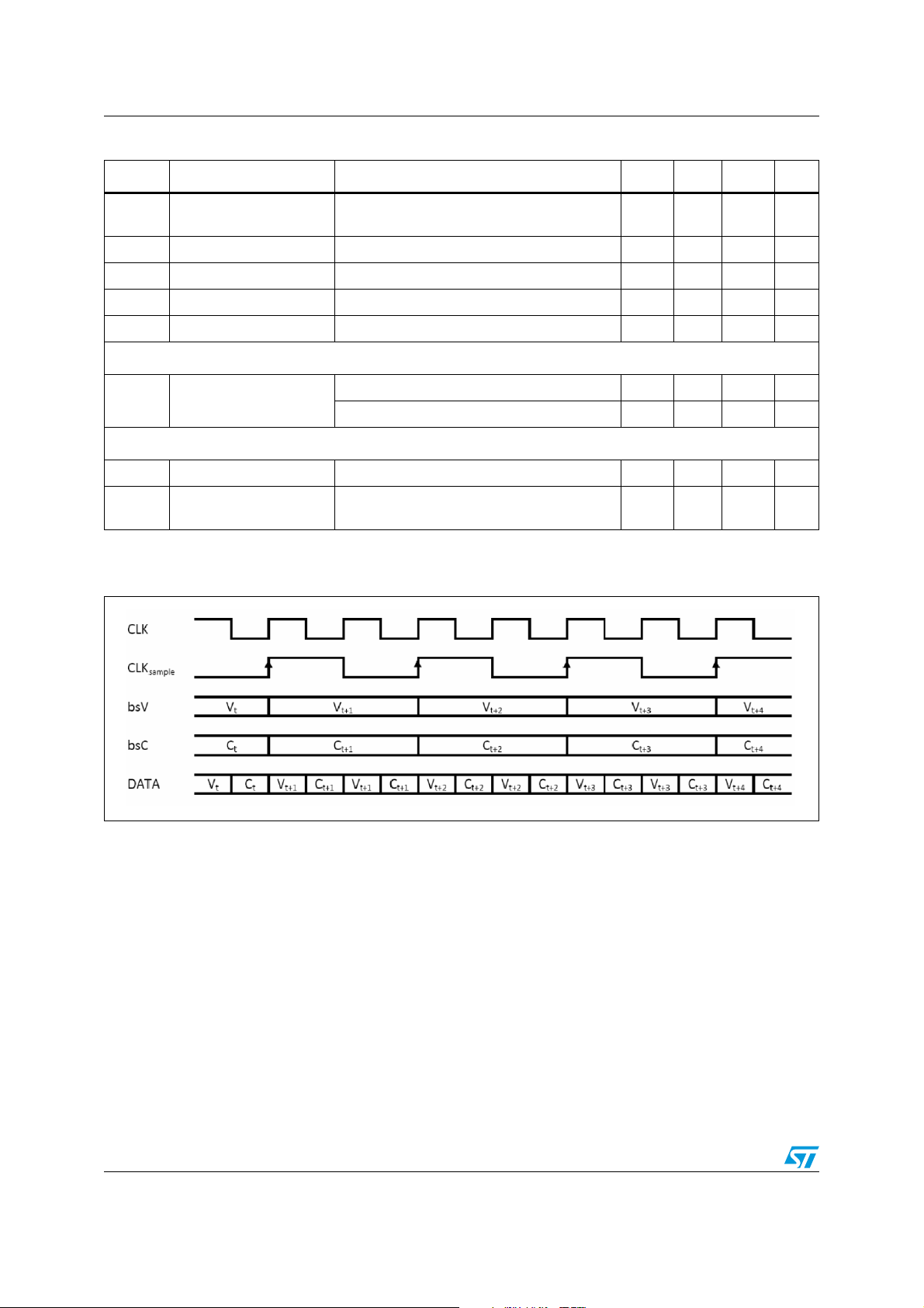
Figure 3. Timing diagram
Reference voltage 1.21 1.23 1.25 V
REF
T
Temperature coefficient After calibration 30 50
C
Low precision 1.0 1.228 MHz
High precision 2.0 2.458 MHz
ppm/
°C
AM07832v1AM07832v1
CLK - clock signal on CLK pin
CLK
bsV - sigma-delta bitstream of voltage signal
bsC - sigma-delta bitstream of current signal
DATA - multiplexed data of voltage and current signal on DAT pin
- sigma-delta sample frequency
sample
8/23 Doc ID 16524 Rev 2
Page 9
STPMS1 Application
5 Application
The choice of external components in the transduction section of the application is a crucial
point in the application design, affecting the precision and the resolution of the whole
system.
Among the several considerations, a compromise must be found between the following
needs:
1. Maximize the signal to noise ratio in the voltage and current channel
2. Choose the current to voltage conversion ratio Ks and the voltage divider ratio in a way
that calibration can be achieved (see also the AN2299; Fast digital calibration
procedure for STPM01 based energy meters, application note)
3. Choose Ks to take advantage of the whole current dynamic range according to desired
maximum current and resolution.
To maximize the signal to noise ratio of the current channel the voltage divider resistors ratio
should be as close as possible to that shown in Ta bl e 6 .
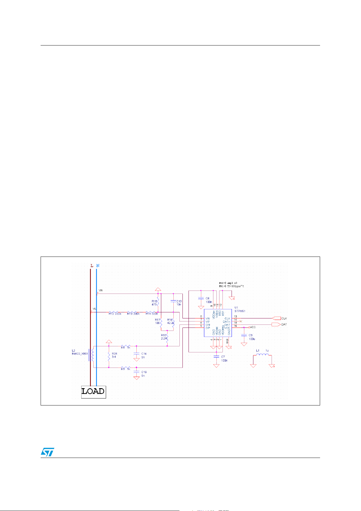
Figure 4 below shows a reference schematic for an application with the following properties:
● P = 64000 imp/kWh
● INOM = 5 A
● IMAX = 60 A
Typical values for the current sensors sensitivity are indicated in Ta bl e 6.
Figure 4. Timing diagram
AM07833v1AM07833v1
Doc ID 16524 Rev 2 9/23
Page 10
Application STPMS1
Table 6. Suggested external components in metering applications
Function Component Description Value Tolerance Unit
Calculator STPMC1 --- --- --- ---
Line voltage
interface
Line current
interface
Resistor
divider
R to R ratio V
R to R ratio V
Rogowski coil Current to voltage ratio K
CT 1.7 ±5 %
=230 V 1:1650 ±1 % 50 ppm/°C V/V
RMS
=110 V 1:830
RMS
0.15 ±5 % 50 ppm/°C mV/A
S
Shunt 0.43 ±5 %
Note: The above listed components refer to typical metering applications. However, STPMS1
operation is not limited to the choice of these external components.
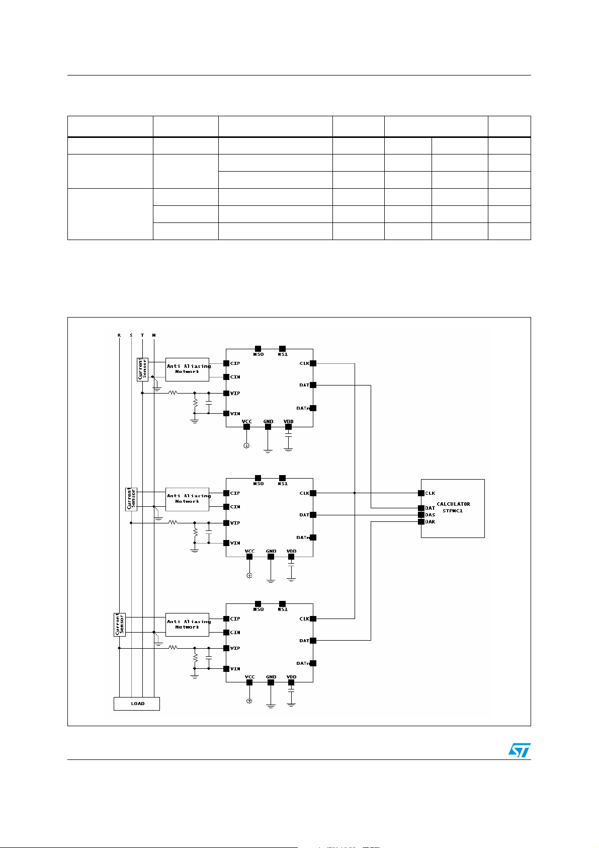
Figure 5. Simplified application schematics for STPMC1 based energy metering
10/23 Doc ID 16524 Rev 2
AM07834v1AM07834v1
Page 11
STPMS1 Application
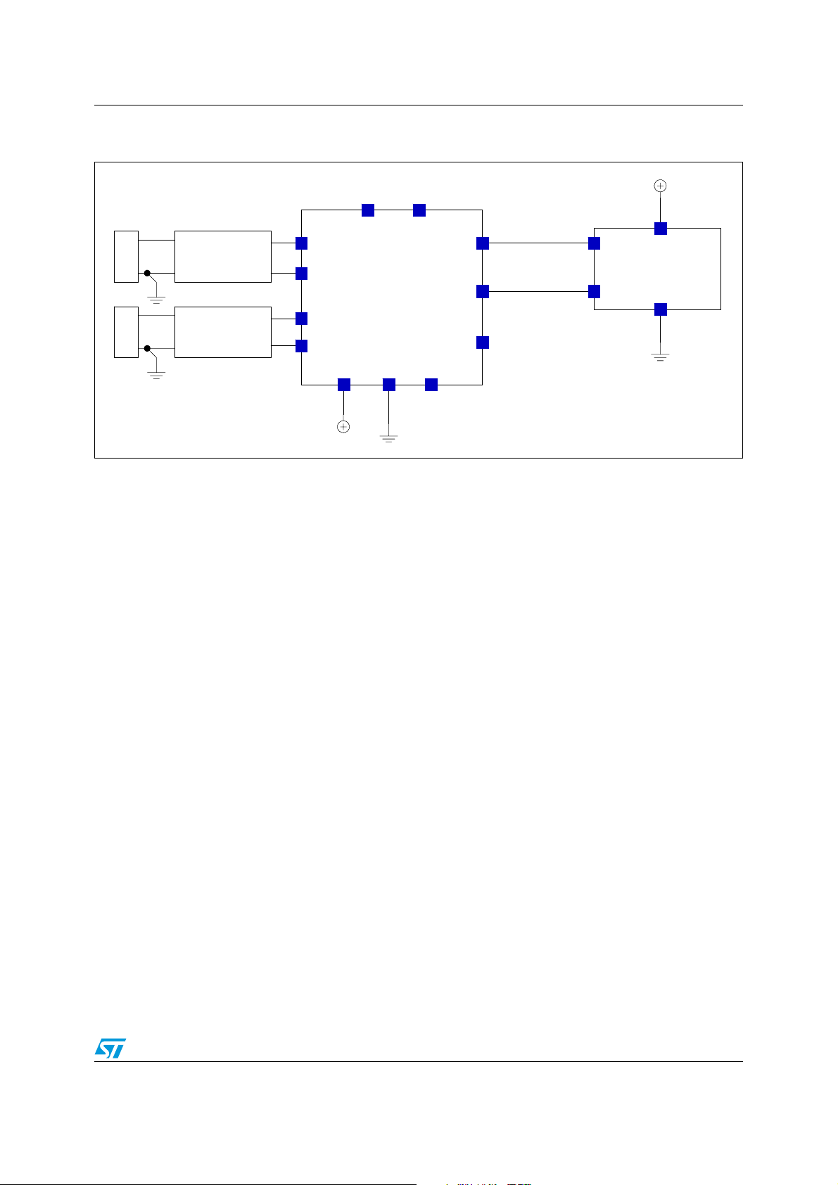
Figure 6. Connection schematic for DSP based applications
1
1
Sensor
Sensor
2
2
Sensor
Sensor
Anti Aliasing
Anti Aliasing
Network
Network
Anti Aliasing
Anti Aliasing
Network
Network
CIP
CIP
CIN
CIN
VIP
VIP
VIN
VIN
MS0
MS0
MS1
MS1
CLKOUT
CLK
CLK
DAT
DAT
DATn
DATn
GND VDDVCC
GND VDDVCC
CLKOUT
DATIN
DATIN
DSP
DSP
AM07835v1
AM07835v1
Doc ID 16524 Rev 2 11/23
Page 12

Terminology STPMS1
6 Terminology
6.1 Conventions
The lowest analog and digital power supply voltage is named GND which represents the
system Ground. All voltage specifications for digital input/output pins are referred to GND.
Positive currents flow into a pin. Sinking current means that the current is flowing into the pin
and then it is positive. Sourcing current means that the current is flowing out of the pin and
then it is negative.
Timing specifications of a signal treated by a digital control part are relative to CLK. This
signal is provided from the STPMC1 calculator IC of 1.024 MHz or of 2.048 MHz nominal
frequency.
A positive logic convention is used in all equations.
6.2 Notation
Current and voltage signals are represented as u and i.
12/23 Doc ID 16524 Rev 2
Page 13
STPMS1 Typical performance characteristics
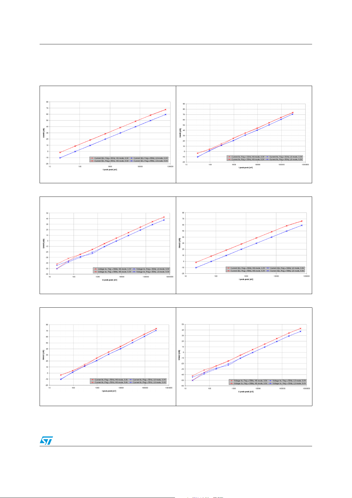
7 Typical performance characteristics
Figure 7. SNRH of CIP-CIN channel, gain 32x Figure 8. SNHR of CIP-CIN channel, gain 8x
Figure 9. SNHR of VIP-VIN channel Figure 10. SINAD of CIP-CIN channel, gain 32x
Figure 11. SINAD of CIP-CIN channel, gain 8x Figure 12. SINAD of VIP-VIN channel
Doc ID 16524 Rev 2 13/23
Page 14
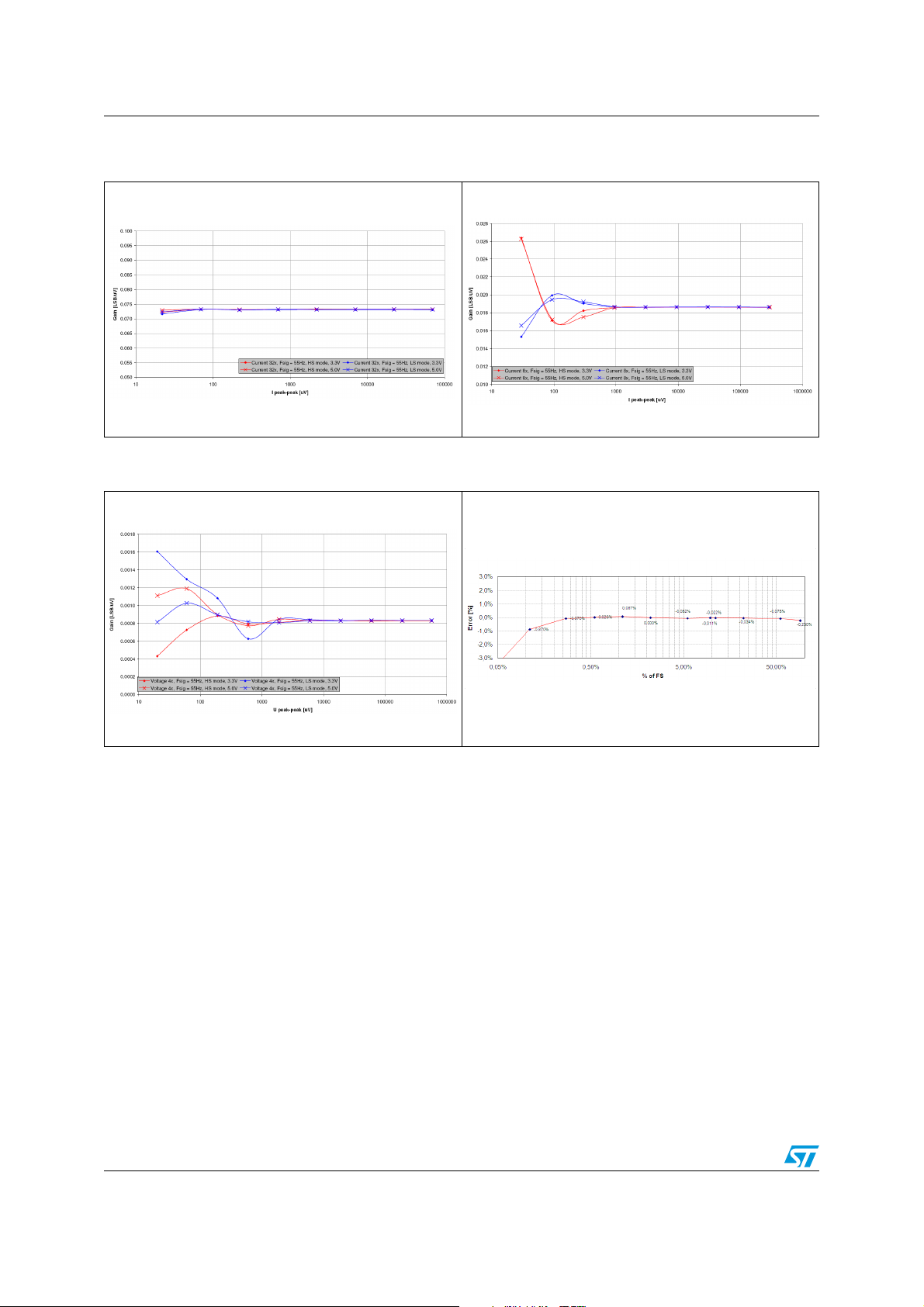
Typical performance characteristics STPMS1
Figure 13. Relative gain error of CIP-CIN
channel, gain 32x
Figure 15. Relative gain error of VIP-VIN
channel
Figure 14. Relative gain error of CIP-CIN
channel, gain 8x
Figure 16. Accuracy over dynamic range
14/23 Doc ID 16524 Rev 2
Page 15

STPMS1 Theory of operation
8 Theory of operation
8.1 General operation description
The STPMS1 performs first-order analog modulation of signals which have frequencies
varying from DC to 2 kHz on two independent channels in parallel. There is a current
channel for measuring line current and a voltage channel for measuring line voltage. The
outputs of the converters provide two streams of digital ones and zeros which are therefore
multiplexed in time to reduce the number of external connections.
The sampling and the data multiplexing are driven by an external clock signal, as it is used
to strobe the analog inputs. The combination of one or more STPMS1s and an STPMC1
(which implements the digital filtering) constitutes a conversion system for energy metering
applications.
The STPMS1 can also be used along with a DSP programmed to demultiplex the output
bitstream and to implement the digital filtering as a medium resolution ADC system.
When used in energy metering applications, the voltage channel is connected externally and
differentially to a line voltage divider which provides an analog signal proportional to the
voltage u. The current channel is connected to a Rogowski coil, or to a current transformer
(CT) or a shunt, which are used to interface the line current. The Rogowski coil provides an
analog signal proportional to di/dt, while the shunt or CT provides an analog signal
proportional to the current i. A CT differs from a shunt in sensitivity and phase error. There
should be an anti-aliasing LP filter inserted between the sensors and the inputs of both
channels of the STPMS1.
Internally, the differential voltage input related to the voltage channel is connected directly to
the A/D converter, which implies an amplification of x4. On the other side, the differential
voltage input related to the current channel is connected first to a configurable x2 or x8 preamplifier and the output of this pre-amplifier to the similar A/D converter (x4 gain), which
implies selectable pre-amplification of x8 or x32 and uses the same reference voltage.
A pair of digital inputs (MS0 and MS1) is used to configure the device.
8.2 Function description of the analog part
The supply pins for the analog part are VCC, VDD, V
The GND pin also represents a reference point. The V
+3.0 V low-drop voltage regulator, the V
while the V
between V
is the digital front-end supply input. A 100 nF capacitor should be connected
DDd
and GND. The input of the mentioned regulator is VCC which powers also a
DDxx
DDac
and V
band-gap, and bias generators.
The analog part consists of several modules:
● Band-gap reference and bias generators
● +3 V low-drop regulator
● two DC buffer amplifiers
● two ΣΔ AD converters
● control signal module
, V
DDac
is an analog I/O pin of an internal
DD
are the modulators supply inputs,
CCav
DDav
, V
DDd
, and GND.
Doc ID 16524 Rev 2 15/23
Page 16
Theory of operation STPMS1
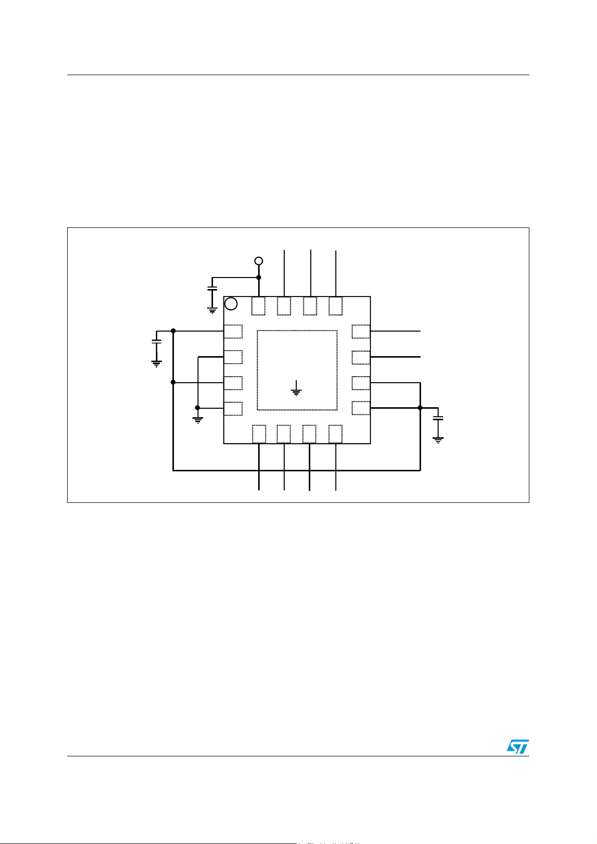
The band-gap voltage reference is used as the reference level source for the low-drop
module and for the AD converters. This module produces several bias currents and voltages
for all other analog modules.
The low-drop regulator generates the +3.0 V power supply level. This level is used to power
the DC buffers, pre-amplifier, and AD converter pair in the analog part of the device and
whole digital part. It is brought out as V
for external connections. As part of low-drop,
DD
there is a power on reset (POR) detection circuit, which blocks all functions of the STPMS1
by asserting the reset condition whenever a V
Figure 17. Power supply external connection scheme
Analog Suppl y
Analog Suppl y
3.3 -5.0V
3.3 -5.0V
100uF
100uF
DAT
DAT
VCC
VCC
VDD
100nF
100nF
VDD
GND
GND
VDD
VDD
GND
GND
supply level is less than +2.5 V.
CC
DATN
CLK
DATN
CLK
MS1
MS1
MS0
MS0
VDD
VDD
VDD
GND
GND
CIN
CIP
CIP
VIP
CIN
VIP
VDD
VIN
VIN
AM07836v1
AM07836v1
100nF
100nF
In order to enable proper operation of the switched capacitor (SC) section of AD converters,
two DC buffers are added to the device. One is buffering the voltage reference level and the
other is buffering the level of value equal to (VDD-VSS)/2.
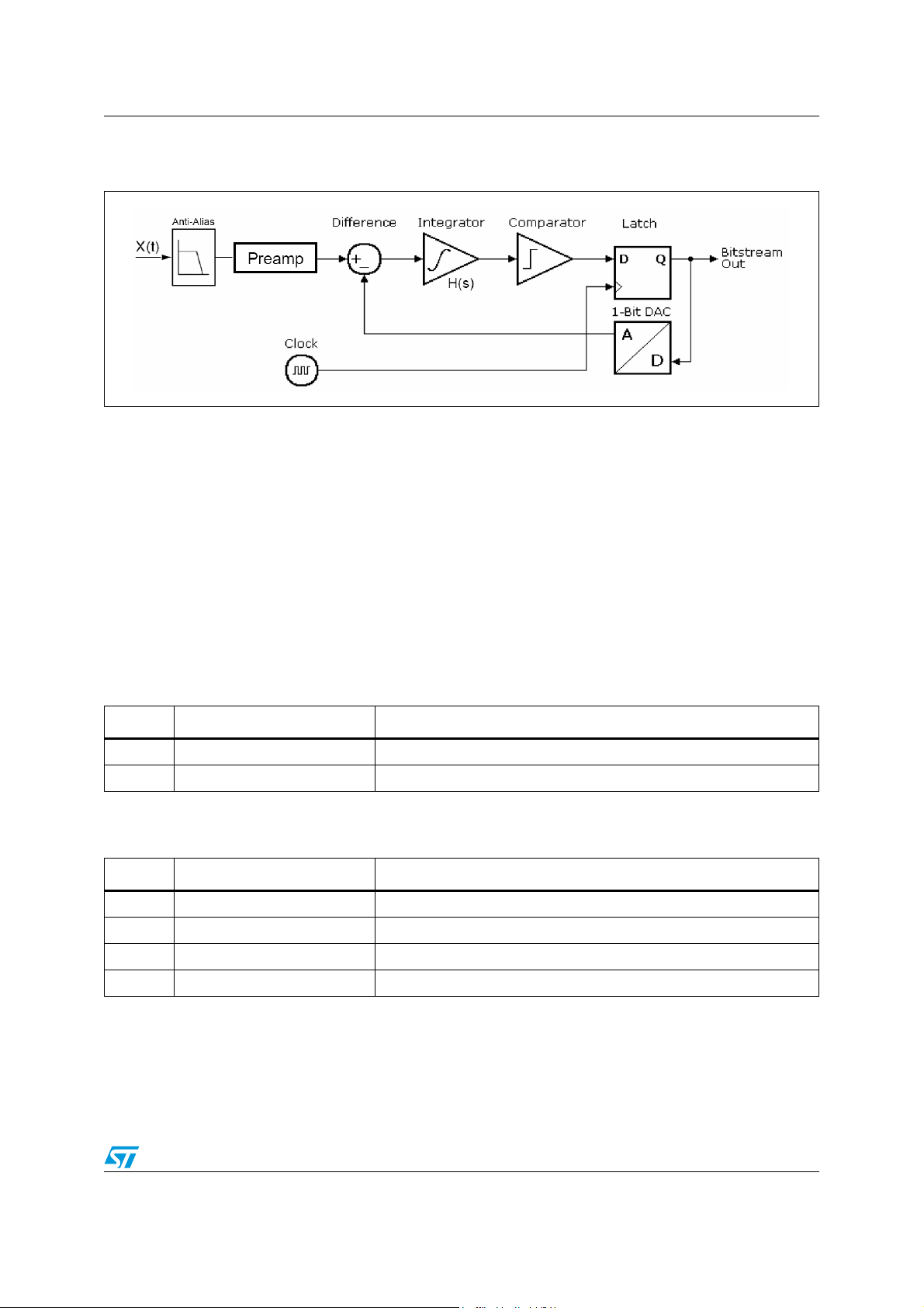
The AD converter block is further split into a voltage and current channel. Each channel
consists of a differential pre-amplifier, SC integrator, comparator, amplifier bias block, and all
necessary switches. The voltage channel SC integrator has a gain of 2 and there is no preamplifier block. The current channel SC integrator has a gain of 2 or 8, which can be
selected by MS0 input, and has a pre-amplifier with a gain of 4.
The amplitude of the input signal to the AD converter block must be kept less than 0.45 V
ref
The output of each channel is input to the digital module as ΣΔ stream.
For the operation of the analog part, a set of five clock signals is provided from the digital
module. These signals derive from the CLK signal. Two of them are used to run the
conversion, the next one is used as the chopper signal for the voltage channel and the last
two are used as chopper signals for the current channel. All these signals are connected to
the control signal module, which consists of standard digital cells powered from an analog
supply. It produces all the necessary signals and switch controls of the AD converters.
.
16/23 Doc ID 16524 Rev 2
Page 17
STPMS1 Theory of operation
Figure 18. Block diagram of the modulator
AM07837v1AM07837v1
8.3 Functional description of the digital part
A digital part is made up of:
● clock generator
● mode decoder
● time multiplex
The clock generator produces all five clocks for the analog module.
The mode decoder generates signals for controlling the temperature coefficient of the onchip band-gap voltage reference and the amplification factor of the current channel, clock
prescaler, and voltage channel enable.
Table 7. Modes of operation
MS0 Mode Description
0 0 ampl = 8
1 1 ampl = 32
Table 8. Changing of band-gap voltage reference
MS1 Mode Description
0 0 TC = 100 ppm/°C
CLK 1 TC = 170 ppm/°C
NCLK 2 TC = 125 ppm/°C
1 3 TC = 190 ppm/°C
The multiplex combines both ΣΔ input signals for the analog module into one signal DAT
which drives differential outputs DAT and DATn according to:
DAT= if CLK then bsV or else bsC
DATN = NOT(DAT).
Doc ID 16524 Rev 2 17/23
Page 18

Package mechanical data STPMS1
9 Package mechanical data
In order to meet environmental requirements, ST offers these devices in different grades of
ECOPACK
specifications, grade definitions, and product status are available at www.st.com. ECOPACK
is an ST registered trademark.
®
packages, depending on their level of environmental compliance. ECOPACK
18/23 Doc ID 16524 Rev 2
Page 19
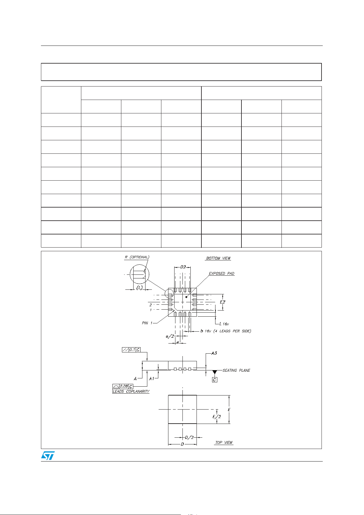
STPMS1 Package mechanical data
QFN16 (3 x 3 mm.) mechanical data
mm. inch.
Dim.
Min. Typ. Max. Min. Typ. Max.
A0.800.90 1.00 0.031 0.035 0.039
A1 0 0.05 0.002
A3 0.20 0.008
b 0.18 0.30 0.007 0.012
D2.90 3.00 3.10 0.114 0.118 0.122
D2 1.50 1.80 0.059 0.071
E 3.00 0.118
E2 2.90 3.00 3.10 0.114 0.118 0.122
e 0.50 0.020
L0.30 0.50 0.012 0.020
7509604/C
Doc ID 16524 Rev 2 19/23
Page 20
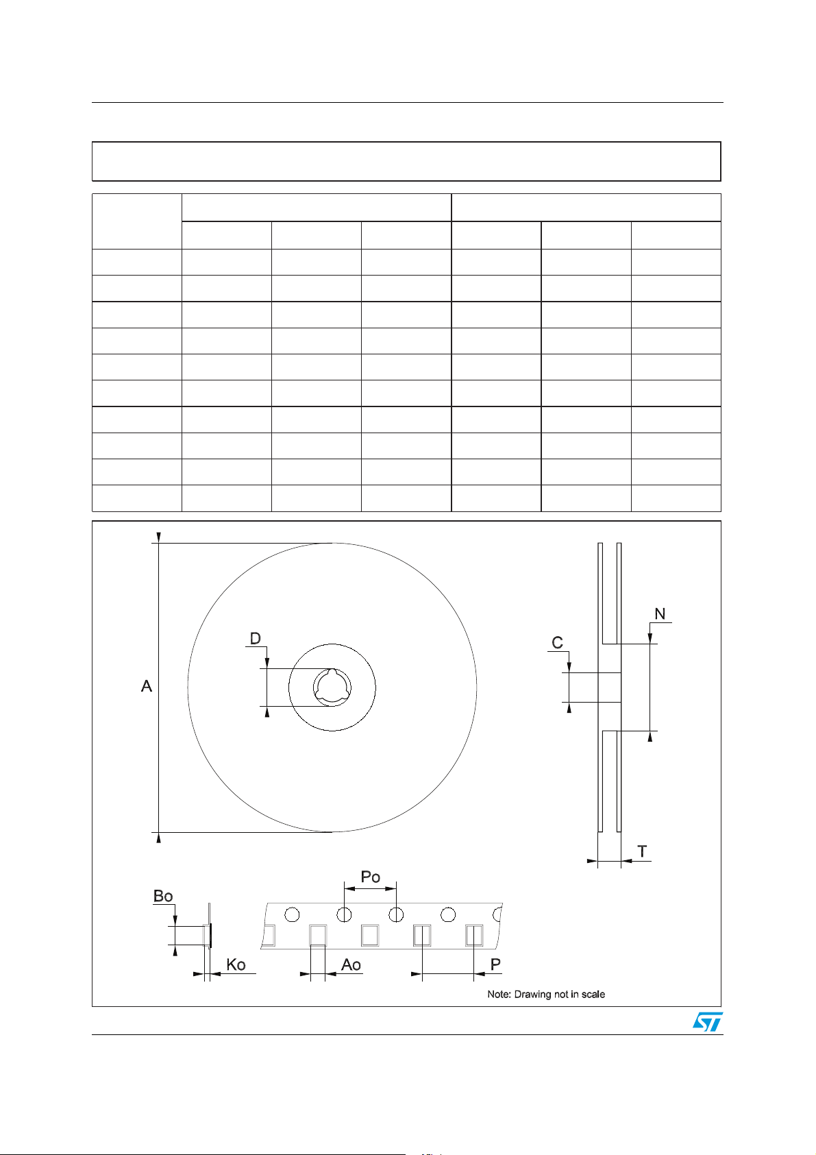
Package mechanical data STPMS1
Tape & reel QFNxx/DFNxx (3 x 3 mm.) mechanical data
mm. inch.
Dim.
Min. Typ. Max. Min. Typ. Max.
A180 7.087
C 12.8 13.2 0.504 0.519
D 20.2 0.795
N60 2.362
T 14.4 0.567
Ao 3.3 0.130
Bo 3.3 0.130
Ko 1.1 0.043
Po 4 0.157
P 8 0.315
20/23 Doc ID 16524 Rev 2
Page 21
STPMS1 Package mechanical data
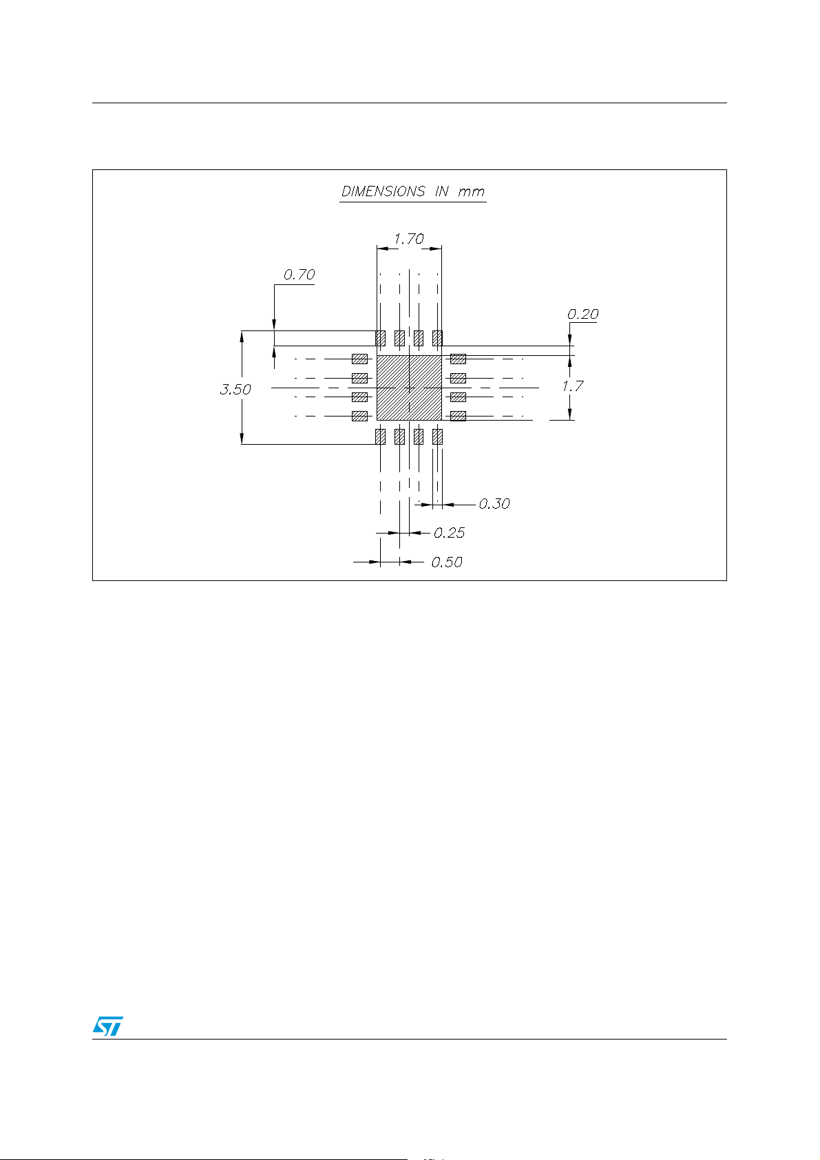
Figure 19. QFN16 (3 x 3 mm) footprint recommended data
Doc ID 16524 Rev 2 21/23
Page 22

Revision history STPMS1
10 Revision history
Table 9. Document revision history
Date Revision Changes
23-Oct-2009 1 Initial release.
07-Oct-2010 2 Data brief header removed from the cover page.
22/23 Doc ID 16524 Rev 2
Page 23

STPMS1
Please Read Carefully:
Information in this document is provided solely in connection with ST products. STMicroelectronics NV and its subsidiaries (“ST”) reserve the
right to make changes, corrections, modifications or improvements, to this document, and the products and services described herein at any
time, without notice.
All ST products are sold pursuant to ST’s terms and conditions of sale.
Purchasers are solely responsible for the choice, selection and use of the ST products and services described herein, and ST assumes no
liability whatsoever relating to the choice, selection or use of the ST products and services described herein.
No license, express or implied, by estoppel or otherwise, to any intellectual property rights is granted under this document. If any part of this
document refers to any third party products or services it shall not be deemed a license grant by ST for the use of such third party products
or services, or any intellectual property contained therein or considered as a warranty covering the use in any manner whatsoever of such
third party products or services or any intellectual property contained therein.
UNLESS OTHERWISE SET FORTH IN ST’S TERMS AND CONDITIONS OF SALE ST DISCLAIMS ANY EXPRESS OR IMPLIED
WARRANTY WITH RESPECT TO THE USE AND/OR SALE OF ST PRODUCTS INCLUDING WITHOUT LIMITATION IMPLIED
WARRANTIES OF MERCHANTABILITY, FITNESS FOR A PARTICULAR PURPOSE (AND THEIR EQUIVALENTS UNDER THE LAWS
OF ANY JURISDICTION), OR INFRINGEMENT OF ANY PATENT, COPYRIGHT OR OTHER INTELLECTUAL PROPERTY RIGHT.
UNLESS EXPRESSLY APPROVED IN WRITING BY AN AUTHORIZED ST REPRESENTATIVE, ST PRODUCTS ARE NOT
RECOMMENDED, AUTHORIZED OR WARRANTED FOR USE IN MILITARY, AIR CRAFT, SPACE, LIFE SAVING, OR LIFE SUSTAINING
APPLICATIONS, NOR IN PRODUCTS OR SYSTEMS WHERE FAILURE OR MALFUNCTION MAY RESULT IN PERSONAL INJURY,
DEATH, OR SEVERE PROPERTY OR ENVIRONMENTAL DAMAGE. ST PRODUCTS WHICH ARE NOT SPECIFIED AS "AUTOMOTIVE
GRADE" MAY ONLY BE USED IN AUTOMOTIVE APPLICATIONS AT USER’S OWN RISK.
Resale of ST products with provisions different from the statements and/or technical features set forth in this document shall immediately void
any warranty granted by ST for the ST product or service described herein and shall not create or extend in any manner whatsoever, any
liability of ST.
ST and the ST logo are trademarks or registered trademarks of ST in various countries.
Information in this document supersedes and replaces all information previously supplied.
The ST logo is a registered trademark of STMicroelectronics. All other names are the property of their respective owners.
© 2010 STMicroelectronics - All rights reserved
STMicroelectronics group of companies
Australia - Belgium - Brazil - Canada - China - Czech Republic - Finland - France - Germany - Hong Kong - India - Israel - Italy - Japan -
Malaysia - Malta - Morocco - Philippines - Singapore - Spain - Sweden - Switzerland - United Kingdom - United States of America
www.st.com
Doc ID 16524 Rev 2 23/23
 Loading...