

Enhanced single channel power switches
Features
■ 90 mΩ high-side MOSFET switch
■ 500/1000 mA continuous current
■ Thermal and short-circuit protection with
overcurrent logic output
■ Operating range from 2.7 V to 5.5 V
■ CMOS- and TTL-compatible enable inputs
■ Undervoltage lockout (UVLO)
■ 12 µA maximum standby supply current
■ Ambient temperature range, -40°C to 85°C
■ 8 kV ESD protection
■ Reverse current protection
■ Fault-blanking
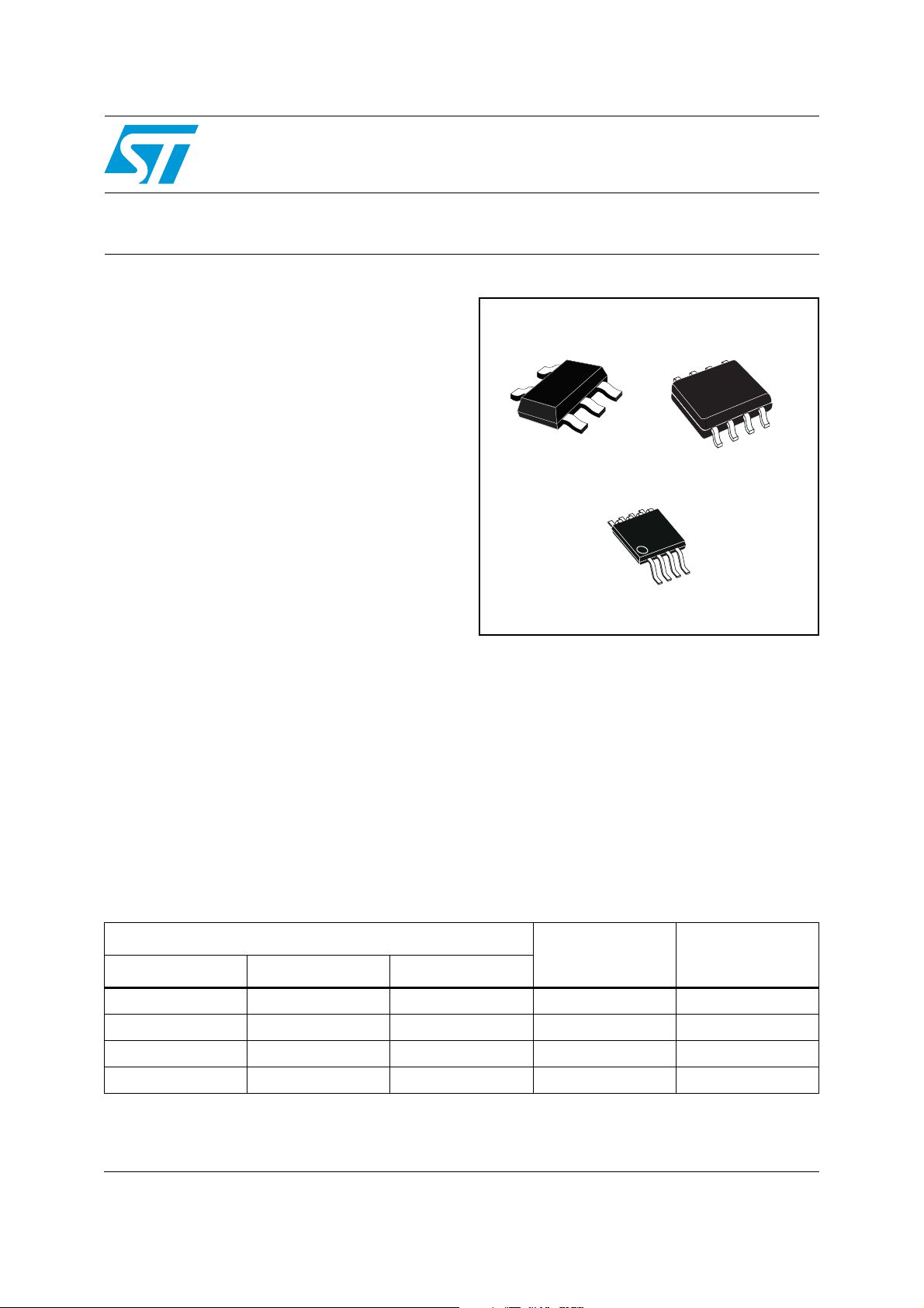
STMPS2141, STMPS2151
STMPS2161, STMPS2171
SOT23-5L
MSOP8
SO-8
Description
The STMPS2141, STMPS2151, STMPS2161,
STMPS2171 power distribution switches are
intended for applications where heavy capacitive
loads and short circuits are likely to be
encountered. These devices incorporate 90 mΩ
N-channel MOSFET high-side power switches for
power-distribution. These switches are controlled
by a logic enable input.
When the output load exceeds the current-limit
threshold or a short is present, the device limits
the output current to a safe level by switching into
a constant-current mode. When continuous heavy
overloads and short circuits increase the power
dissipation in the switch, causing the junction
temperature to rise, a thermal protection circuit
shuts the switch off to prevent damage. Recovery
from a thermal shutdown is automatic once the
device has cooled sufficiently. Internal circuitry
ensures the switch remains off until a valid input
voltage is present.
Table 1. Device summary
Order codes
SO-8 SOT23-5L MSOP8
STMPS2141MTR STMPS2141STR STMPS2141TTR 500 Active low
STMPS2151MTR STMPS2151STR STMPS2151TTR 500 Active high
STMPS2161MTR STMPS2161STR STMPS2161TTR 1000 Active low
STMPS2171MTR STMPS2171STR STMPS2171TTR 1000 Active high
1. MSOP8 package is also known as “TSSOP8”
(1)
Current limit
(mA)
Enable
July 2009 Doc ID 13793 Rev 4 1/34
www.st.com
34

Contents STMPS2141, STMPS2151, STMPS2161, STMPS2171
Contents
1 Block diagram . . . . . . . . . . . . . . . . . . . . . . . . . . . . . . . . . . . . . . . . . . . . . . 7
2 Pin settings . . . . . . . . . . . . . . . . . . . . . . . . . . . . . . . . . . . . . . . . . . . . . . . . 8
2.1 Pin connections . . . . . . . . . . . . . . . . . . . . . . . . . . . . . . . . . . . . . . . . . . . . . 8
2.2 Pin description . . . . . . . . . . . . . . . . . . . . . . . . . . . . . . . . . . . . . . . . . . . . . . 8
3 Functional description . . . . . . . . . . . . . . . . . . . . . . . . . . . . . . . . . . . . . . . 9
3.1 Fault blanking . . . . . . . . . . . . . . . . . . . . . . . . . . . . . . . . . . . . . . . . . . . . . . . 9
3.2 Overcurrent/over-temperature protection . . . . . . . . . . . . . . . . . . . . . . . . . . 9
3.3 FAULT conditions . . . . . . . . . . . . . . . . . . . . . . . . . . . . . . . . . . . . . . . . . . . . 9
3.4 Reversed current blocking . . . . . . . . . . . . . . . . . . . . . . . . . . . . . . . . . . . . 10
3.5 UVLO . . . . . . . . . . . . . . . . . . . . . . . . . . . . . . . . . . . . . . . . . . . . . . . . . . . . 10
4 Ambient temperature . . . . . . . . . . . . . . . . . . . . . . . . . . . . . . . . . . . . . . . 11
5 Maximum ratings . . . . . . . . . . . . . . . . . . . . . . . . . . . . . . . . . . . . . . . . . . . 12
5.1 Absolute maximum ratings . . . . . . . . . . . . . . . . . . . . . . . . . . . . . . . . . . . . 12
5.2 Recommended operating conditions . . . . . . . . . . . . . . . . . . . . . . . . . . . . 12
6 Electrical specifications . . . . . . . . . . . . . . . . . . . . . . . . . . . . . . . . . . . . . 13
7 Detail device characteristics . . . . . . . . . . . . . . . . . . . . . . . . . . . . . . . . . 16
7.1 STMPS2141, STMPS2151 additional electrical charts . . . . . . . . . . . . . . 16
7.1.1 Turn on/off characteristics at VOUT = 5.0 V . . . . . . . . . . . . . . . . . . . . . 16
7.1.2 Turn on/off characteristics at VOUT = 3.0 V . . . . . . . . . . . . . . . . . . . . . 17
7.1.3 UVLO . . . . . . . . . . . . . . . . . . . . . . . . . . . . . . . . . . . . . . . . . . . . . . . . . . . 17
7.1.4 OC protection characteristics . . . . . . . . . . . . . . . . . . . . . . . . . . . . . . . . 18
7.1.5 Other electrical characteristics . . . . . . . . . . . . . . . . . . . . . . . . . . . . . . . . 18
7.2 STMPS2161, STMPS2171 electrical charts . . . . . . . . . . . . . . . . . . . . . . 21
7.2.1 Turn on/off characteristics at VOUT = 5.0 V . . . . . . . . . . . . . . . . . . . . . 21
7.2.2 Turn on/off characteristics at VOUT = 3.0 V . . . . . . . . . . . . . . . . . . . . . 22
7.2.3 UVLO . . . . . . . . . . . . . . . . . . . . . . . . . . . . . . . . . . . . . . . . . . . . . . . . . . . 22
7.2.4 OC protection characteristics . . . . . . . . . . . . . . . . . . . . . . . . . . . . . . . . 23
7.2.5 Other electrical characteristics . . . . . . . . . . . . . . . . . . . . . . . . . . . . . . . . 24
2/34 Doc ID 13793 Rev 4

STMPS2141, STMPS2151, STMPS2161, STMPS2171 Contents
8 Package mechanical data . . . . . . . . . . . . . . . . . . . . . . . . . . . . . . . . . . . . 26
9 Revision history . . . . . . . . . . . . . . . . . . . . . . . . . . . . . . . . . . . . . . . . . . . 33
Doc ID 13793 Rev 4 3/34

List of figures STMPS2141, STMPS2151, STMPS2161, STMPS2171
List of figures
Figure 1. Block diagram . . . . . . . . . . . . . . . . . . . . . . . . . . . . . . . . . . . . . . . . . . . . . . . . . . . . . . . . . . . . 6
Figure 2. SOT23-5L, SO-8 and MSOP8 pin connections . . . . . . . . . . . . . . . . . . . . . . . . . . . . . . . . . . 7
Figure 3. Voltage output turn on delay time . . . . . . . . . . . . . . . . . . . . . . . . . . . . . . . . . . . . . . . . . . . . 15
Figure 4. Voltage output turn off delay time . . . . . . . . . . . . . . . . . . . . . . . . . . . . . . . . . . . . . . . . . . . . 15
Figure 5. Current output turn on delay time . . . . . . . . . . . . . . . . . . . . . . . . . . . . . . . . . . . . . . . . . . . . 15
Figure 6. Current output turn off delay time . . . . . . . . . . . . . . . . . . . . . . . . . . . . . . . . . . . . . . . . . . . . 15
Figure 7. Voltage output turn on delay time . . . . . . . . . . . . . . . . . . . . . . . . . . . . . . . . . . . . . . . . . . . . 16
Figure 8. Voltage output turn off delay time . . . . . . . . . . . . . . . . . . . . . . . . . . . . . . . . . . . . . . . . . . . . 16
Figure 9. Current output turn on delay time . . . . . . . . . . . . . . . . . . . . . . . . . . . . . . . . . . . . . . . . . . . . 16
Figure 10. Current output turn off delay time . . . . . . . . . . . . . . . . . . . . . . . . . . . . . . . . . . . . . . . . . . . . 16
Figure 11. UVLO rising . . . . . . . . . . . . . . . . . . . . . . . . . . . . . . . . . . . . . . . . . . . . . . . . . . . . . . . . . . . . 16
Figure 12. UVLO falling . . . . . . . . . . . . . . . . . . . . . . . . . . . . . . . . . . . . . . . . . . . . . . . . . . . . . . . . . . . . 16
Figure 13. OC protection at VOUT = 3.0 V . . . . . . . . . . . . . . . . . . . . . . . . . . . . . . . . . . . . . . . . . . . . . 17
Figure 14. OC protection at VOUT = 3.0 V . . . . . . . . . . . . . . . . . . . . . . . . . . . . . . . . . . . . . . . . . . . . . 17
Figure 15. OC protection at VOUT = 5.0 V . . . . . . . . . . . . . . . . . . . . . . . . . . . . . . . . . . . . . . . . . . . . . 17
Figure 16. OC protection at VOUT = 5.0 V . . . . . . . . . . . . . . . . . . . . . . . . . . . . . . . . . . . . . . . . . . . . . 17
Figure 17. ICC vs VIN (enabled) . . . . . . . . . . . . . . . . . . . . . . . . . . . . . . . . . . . . . . . . . . . . . . . . . . . . . 17
Figure 18. ICC vs temperature (enabled) . . . . . . . . . . . . . . . . . . . . . . . . . . . . . . . . . . . . . . . . . . . . . . 17
Figure 19. ICC vs VIN (disabled) . . . . . . . . . . . . . . . . . . . . . . . . . . . . . . . . . . . . . . . . . . . . . . . . . . . . . 18
Figure 20. ICC vs temperature (disabled) . . . . . . . . . . . . . . . . . . . . . . . . . . . . . . . . . . . . . . . . . . . . . . 18
Figure 21. RDS ON vs VIN . . . . . . . . . . . . . . . . . . . . . . . . . . . . . . . . . . . . . . . . . . . . . . . . . . . . . . . . . 18
Figure 22. RDS ON vs temperature . . . . . . . . . . . . . . . . . . . . . . . . . . . . . . . . . . . . . . . . . . . . . . . . . . . 18
Figure 23. ILIMIT vs temperature. . . . . . . . . . . . . . . . . . . . . . . . . . . . . . . . . . . . . . . . . . . . . . . . . . . . . 18
Figure 24. Switch leakage vs temperature. . . . . . . . . . . . . . . . . . . . . . . . . . . . . . . . . . . . . . . . . . . . . . 18
Figure 25. Output rise time vs. VIN . . . . . . . . . . . . . . . . . . . . . . . . . . . . . . . . . . . . . . . . . . . . . . . . . . . 19
Figure 26. Output fall time vs. VIN . . . . . . . . . . . . . . . . . . . . . . . . . . . . . . . . . . . . . . . . . . . . . . . . . . . . 19
Figure 27. UVLO vs temperature . . . . . . . . . . . . . . . . . . . . . . . . . . . . . . . . . . . . . . . . . . . . . . . . . . . . . 19
Figure 28. Voltage output turn on delay time . . . . . . . . . . . . . . . . . . . . . . . . . . . . . . . . . . . . . . . . . . . . 20
Figure 29. Voltage output turn off delay time . . . . . . . . . . . . . . . . . . . . . . . . . . . . . . . . . . . . . . . . . . . . 20
Figure 30. Current output turn on delay time . . . . . . . . . . . . . . . . . . . . . . . . . . . . . . . . . . . . . . . . . . . . 20
Figure 31. Current output turn off delay time . . . . . . . . . . . . . . . . . . . . . . . . . . . . . . . . . . . . . . . . . . . . 20
Figure 32. Voltage output turn on delay time . . . . . . . . . . . . . . . . . . . . . . . . . . . . . . . . . . . . . . . . . . . . 21
Figure 33. Voltage output turn off delay time . . . . . . . . . . . . . . . . . . . . . . . . . . . . . . . . . . . . . . . . . . . . 21
Figure 34. Current output turn on delay time . . . . . . . . . . . . . . . . . . . . . . . . . . . . . . . . . . . . . . . . . . . . 21
Figure 35. Current output turn off delay time . . . . . . . . . . . . . . . . . . . . . . . . . . . . . . . . . . . . . . . . . . . . 21
Figure 36. UVLO rising . . . . . . . . . . . . . . . . . . . . . . . . . . . . . . . . . . . . . . . . . . . . . . . . . . . . . . . . . . . . 21
Figure 37. UVLO falling . . . . . . . . . . . . . . . . . . . . . . . . . . . . . . . . . . . . . . . . . . . . . . . . . . . . . . . . . . . . 21
Figure 38. OC protection at VOUT = 3.0 V . . . . . . . . . . . . . . . . . . . . . . . . . . . . . . . . . . . . . . . . . . . . . 22
Figure 39. OC protection at VOUT = 3.0 V . . . . . . . . . . . . . . . . . . . . . . . . . . . . . . . . . . . . . . . . . . . . . 22
Figure 40. OC protection at VOUT = 5.0 V . . . . . . . . . . . . . . . . . . . . . . . . . . . . . . . . . . . . . . . . . . . . . 22
Figure 41. OC protection at VOUT = 5.0 V . . . . . . . . . . . . . . . . . . . . . . . . . . . . . . . . . . . . . . . . . . . . . 22
Figure 42. ICC vs VIN (enabled) . . . . . . . . . . . . . . . . . . . . . . . . . . . . . . . . . . . . . . . . . . . . . . . . . . . . . 23
Figure 43. ICC vs temperature (enabled) . . . . . . . . . . . . . . . . . . . . . . . . . . . . . . . . . . . . . . . . . . . . . . 23
Figure 44. ICC vs VIN (disabled) . . . . . . . . . . . . . . . . . . . . . . . . . . . . . . . . . . . . . . . . . . . . . . . . . . . . . 23
Figure 45. ICC vs temperature (disabled) . . . . . . . . . . . . . . . . . . . . . . . . . . . . . . . . . . . . . . . . . . . . . . 23
Figure 46. RDS ON vs VIN . . . . . . . . . . . . . . . . . . . . . . . . . . . . . . . . . . . . . . . . . . . . . . . . . . . . . . . . . 23
Figure 47. RDS ON vs temperature . . . . . . . . . . . . . . . . . . . . . . . . . . . . . . . . . . . . . . . . . . . . . . . . . . . 23
Figure 48. ILIMIT vs temperature. . . . . . . . . . . . . . . . . . . . . . . . . . . . . . . . . . . . . . . . . . . . . . . . . . . . . 24
4/34 Doc ID 13793 Rev 4

STMPS2141, STMPS2151, STMPS2161, STMPS2171 List of figures
Figure 49. Switch leakage vs temperature. . . . . . . . . . . . . . . . . . . . . . . . . . . . . . . . . . . . . . . . . . . . . . 24
Figure 50. Output rise time vs. VIN . . . . . . . . . . . . . . . . . . . . . . . . . . . . . . . . . . . . . . . . . . . . . . . . . . . 24
Figure 51. Output fall time vs. VIN . . . . . . . . . . . . . . . . . . . . . . . . . . . . . . . . . . . . . . . . . . . . . . . . . . . . 24
Figure 52. UVLO vs temperature . . . . . . . . . . . . . . . . . . . . . . . . . . . . . . . . . . . . . . . . . . . . . . . . . . . . . 24
Figure 53. SOT23-5L package outline . . . . . . . . . . . . . . . . . . . . . . . . . . . . . . . . . . . . . . . . . . . . . . . . . 25
Figure 54. SOT23-5L footprint recommendations . . . . . . . . . . . . . . . . . . . . . . . . . . . . . . . . . . . . . . . . 26
Figure 55. SOT23-5L carrier tape . . . . . . . . . . . . . . . . . . . . . . . . . . . . . . . . . . . . . . . . . . . . . . . . . . . . 26
Figure 56. SOT23-5L reel information . . . . . . . . . . . . . . . . . . . . . . . . . . . . . . . . . . . . . . . . . . . . . . . . . 27
Figure 57. SO-8 package outline . . . . . . . . . . . . . . . . . . . . . . . . . . . . . . . . . . . . . . . . . . . . . . . . . . . . . 28
Figure 58. MSOP8 package outline . . . . . . . . . . . . . . . . . . . . . . . . . . . . . . . . . . . . . . . . . . . . . . . . . . . 29
Figure 59. SO-8 carrier tape . . . . . . . . . . . . . . . . . . . . . . . . . . . . . . . . . . . . . . . . . . . . . . . . . . . . . . . . 30
Figure 60. MSOP8 carrier tape . . . . . . . . . . . . . . . . . . . . . . . . . . . . . . . . . . . . . . . . . . . . . . . . . . . . . . 30
Figure 61. Reel information . . . . . . . . . . . . . . . . . . . . . . . . . . . . . . . . . . . . . . . . . . . . . . . . . . . . . . . . . 31
Doc ID 13793 Rev 4 5/34

List of tables STMPS2141, STMPS2151, STMPS2161, STMPS2171
List of tables
Table 1. Device summary . . . . . . . . . . . . . . . . . . . . . . . . . . . . . . . . . . . . . . . . . . . . . . . . . . . . . . . . . . 1
Table 2. Pin description . . . . . . . . . . . . . . . . . . . . . . . . . . . . . . . . . . . . . . . . . . . . . . . . . . . . . . . . . . . 8
Table 3. FAULT conditions . . . . . . . . . . . . . . . . . . . . . . . . . . . . . . . . . . . . . . . . . . . . . . . . . . . . . . . . . 9
Table 4. SOT23-5L (160 °C/W) . . . . . . . . . . . . . . . . . . . . . . . . . . . . . . . . . . . . . . . . . . . . . . . . . . . . 11
Table 5. MSOP8 (220 °C/W) . . . . . . . . . . . . . . . . . . . . . . . . . . . . . . . . . . . . . . . . . . . . . . . . . . . . . . 11
Table 6. SO-8 (160 °C/W). . . . . . . . . . . . . . . . . . . . . . . . . . . . . . . . . . . . . . . . . . . . . . . . . . . . . . . . . 11
Table 7. Absolute maximum ratings . . . . . . . . . . . . . . . . . . . . . . . . . . . . . . . . . . . . . . . . . . . . . . . . . 12
Table 8. Recommended operating conditions . . . . . . . . . . . . . . . . . . . . . . . . . . . . . . . . . . . . . . . . . 12
Table 9. SOT-23-5L electrical characteristics . . . . . . . . . . . . . . . . . . . . . . . . . . . . . . . . . . . . . . . . . . 13
Table 10. MSO8P/SO8 electrical characteristics . . . . . . . . . . . . . . . . . . . . . . . . . . . . . . . . . . . . . . . . 13
Table 11. Current limit characteristics
(VI = 5.5 V, IO = rated current, TJ = 25°C, unless otherwise specified) . . . . . . . . . . . . . . . 14
Table 12. Supply current characteristics
(VI = 5.5 V, IO = rated current, TJ = 25°C, unless otherwise specified) . . . . . . . . . . . . . . . 14
Table 13. Thermal characteristics
(VI = 5.5 V, IO = rated current, TJ = 25°C, unless otherwise specified) . . . . . . . . . . . . . . . 15
Table 14. UVLO characteristics
(VI = 5.5 V, IO = rated current, TJ = 25°C, unless otherwise specified) . . . . . . . . . . . . . . . 15
Table 15. OC pin characteristics
(VI = 5.5 V, IO = rated current, TJ = 25°C, unless otherwise specified) . . . . . . . . . . . . . . . 15
Table 16. EN pin characteristics
(VI = 5.5 V, IO = rated current, TJ = 25°C, unless otherwise specified) . . . . . . . . . . . . . . . 15
Table 17. SOT23-5L mechanical data . . . . . . . . . . . . . . . . . . . . . . . . . . . . . . . . . . . . . . . . . . . . . . . . 26
Table 18. SOT23-5L footprint dimensions . . . . . . . . . . . . . . . . . . . . . . . . . . . . . . . . . . . . . . . . . . . . . 27
Table 19. SO-8 mechanical data . . . . . . . . . . . . . . . . . . . . . . . . . . . . . . . . . . . . . . . . . . . . . . . . . . . . 29
Table 20. MSOP8 package mechanical data . . . . . . . . . . . . . . . . . . . . . . . . . . . . . . . . . . . . . . . . . . . 30
Table 21. Reel mechanical data . . . . . . . . . . . . . . . . . . . . . . . . . . . . . . . . . . . . . . . . . . . . . . . . . . . . . 32
Table 22. Document revision history . . . . . . . . . . . . . . . . . . . . . . . . . . . . . . . . . . . . . . . . . . . . . . . . . 33
6/34 Doc ID 13793 Rev 4
STMPS2141, STMPS2151, STMPS2161, STMPS2171 Block diagram
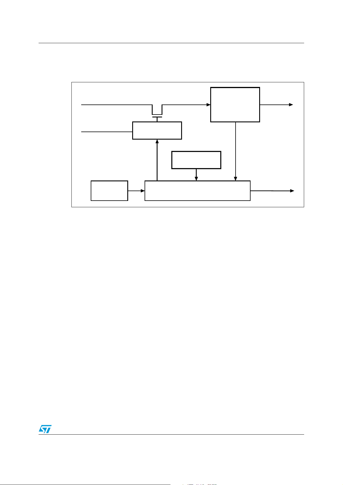
1 Block diagram
Figure 1. Block diagram
V
EN
IN
Thermal
sense
Driver
UVLO
Fault blanking/reporting
driver control unit
Current
sense
V
OUT
Fault
Doc ID 13793 Rev 4 7/34
Pin settings STMPS2141, STMPS2151, STMPS2161, STMPS2171
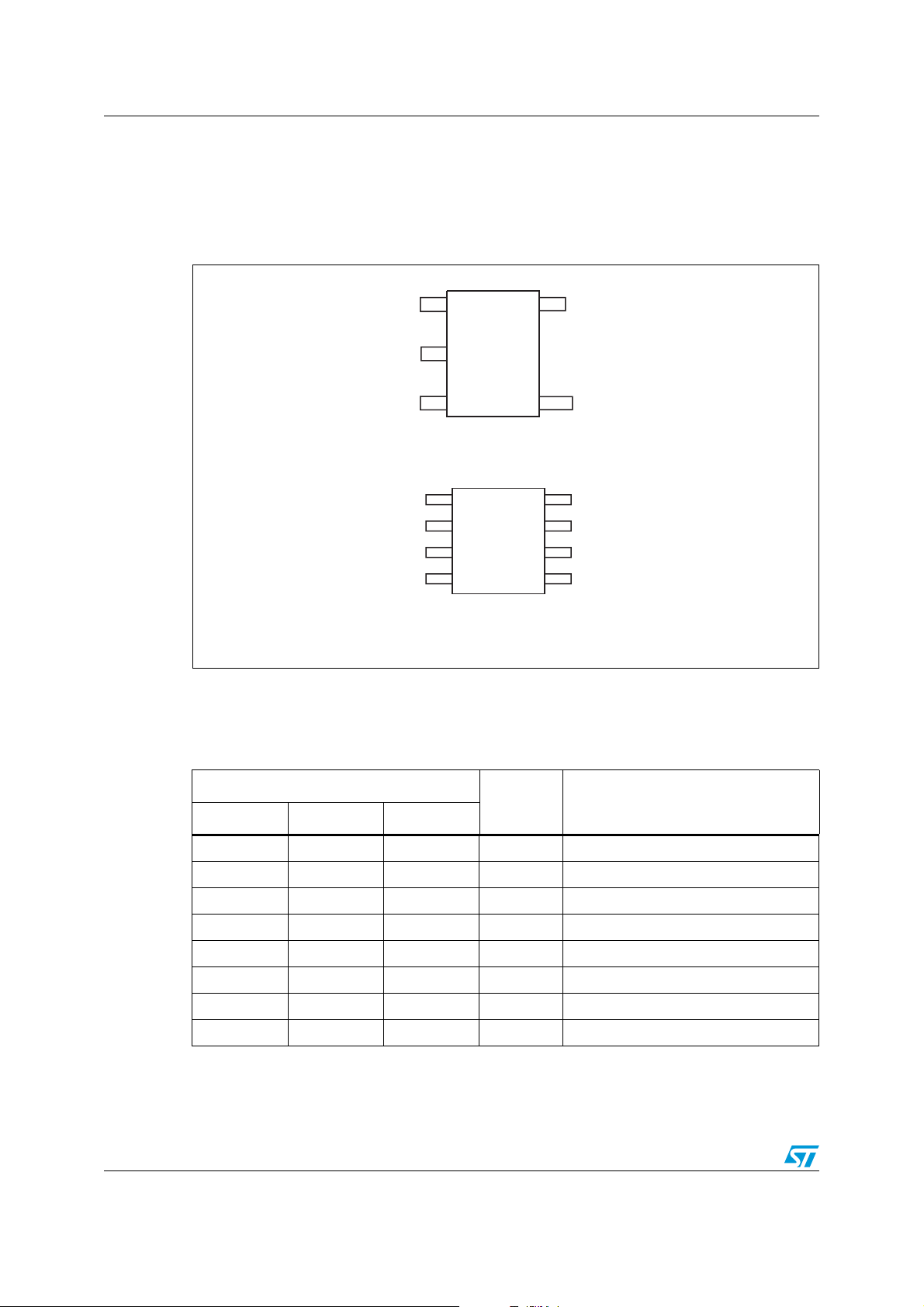
2 Pin settings
2.1 Pin connections
Figure 2. SOT23-5L, SO-8 and MSOP8 pin connections
OUT
GND
FAULT
GND
EN_N
2.2 Pin description
Table 2. Pin description
IN
IN
SO-8 / MSOP8
1
2
3
SOT23-5L
1
2
3
4
5
4
8
7
6
5
IN
EN
OUT
OUT
OUT
FAULT
Pin number
Name Function
SO8 MSOP8 SOT23-5L
1 1 2 GND Ground
2 2 5 IN 2.7 V - 5.5 V input
3 3 - IN 2.7 V - 5.5 V input
4 4 4 EN Enable for power switch
5 5 3 FAULT Open drain FAULT indicator, active low
6 6 1 OUT Output of power switch
7 7 - OUT Output of power switch
8 8 - OUT Output of power switch
8/34 Doc ID 13793 Rev 4
STMPS2141, STMPS2151, STMPS2161, STMPS2171 Functional description
3 Functional description
3.1 Fault blanking
The STMPS devices feature a 10 ms fault blanking. Fault blanking allows current-limit faults,
including momentary short-circuit faults that occur when hot-swapping a capacitive load,
and also ensures that no fault is issued during power-up. When a load transient causes the
device to enter current limit, an internal counter starts. If the load fault persists beyond the
10 ms fault-blanking timeout, the FAULT output asserts “low”. Load-transient faults less than
10 ms (typ.) do not cause a FAULT output assertion. Only current-limit faults are blanked.
Die over-temperature faults and input voltage drops below the UVLO threshold cause an
immediate fault output.
3.2 Overcurrent/over-temperature protection
In overcurrent or short-circuit condition, the switch limits the current at a value of about
120% of the rated current. If the temperature of the die goes above the limit value, the switch
turns off.
3.3 FAULT conditions
In power switch applications, 4 types of FAULT conditions are common. These fault
conditions and the response of the STMPS21x1 power switches are described in the
following Ta bl e 3 .
Table 3. FAULT conditions
Fault Condition STMPS21x1 action
Output shorted to GND via resistance
Short circuit
Over-current
Overheating
Undervoltage
path of < 1 Ω, causing a rapid current
surge.
Output connected to a load that sinks
current above threshold.
Temperature of junction exceeds 135°C
due to any reason.
Input voltage drops below the UVLO
treshold.
Reduces output voltage to reduce the
current. Asserts FAULT pin after a
blanking period
Reduces output voltage to reduce the
current. Asserts FAULT pin after a
blanking period.
Turn OFF output until temperature falls
below 125°C. Asserts FAULT pin
immediately.
Turn OFF output until input voltage rises
above the UVLO treshold plus hysteresis.
Asserts FAULT pin immediately.
Doc ID 13793 Rev 4 9/34

Functional description STMPS2141, STMPS2151, STMPS2161, STMPS2171
3.4 Reversed current blocking
When the switch is OFF (disabled through the EN pin), or when the STMPS device is un-
powered (V
reverse current will flow into the device when V
Note: In the case where the switch is ON, and a voltage higher than V
a reverse current occurs. This operating condition is not allowed.
= 0 V) the switch behaves as an Hi-Z at the output pin, ensuring that no
CC
< Vo .
i
is applied to the OUT pin,
IN
3.5 UVLO
When the input voltage drops below critical values, the power switch turns off to prevent
improper operation due to low voltage.
10/34 Doc ID 13793 Rev 4
STMPS2141, STMPS2151, STMPS2161, STMPS2171 Ambient temperature
4 Ambient temperature
In Enable operating mode, an amount of power is dissipated as heat in the power switch due
to the on-resistance. The power dissipation is: P = I
Table 4. SOT23-5L (160 °C/W)
Part number Max current
STMPS2141
STMPS2151
STMPS2161
STMPS2171
Table 5. MSOP8 (220 °C/W)
Part number
STMPS2141
STMPS2151
Max R
0.50 A 130 mΩ 32.5 mW 6.2 118.8
1.00 A 130 mΩ 130.0 mW 24.8 100.2
Max
current
Max R
at 5 V
0.50 A 130 mΩ 32.5 mW 7.2 117.8
5V
ON
ON
at
Power
dissipation
Power
dissipation
2
R.
Temperature
difference
(junction and
ambient)
Temperature
difference
(junction and
ambient)
Maximum ambient
temperature
(at junction
temperature 125 °C)
Maximum ambient
temperature
(at junction temperature
125 °C)
STMPS2161
1.00 A 130 mΩ 130.0 mW 28.6 96.4
STMPS2171
Table 6. SO-8 (160 °C/W)
Part number Max current
STMPS2141
0.50 A 130 mΩ 32.5 mΩ 5.2 124.8
STMPS2151
STMPS2161
1.00 A 130 mΩ 130.0 mΩ 20.8 104.2
STMPS2171
Max R
at 5 V
ON
Power
dissipation
Temperature
difference (junction
and ambient)
Maximum ambient
temperature
(at junction temperature
125 °C)
Doc ID 13793 Rev 4 11/34

Maximum ratings STMPS2141, STMPS2151, STMPS2161, STMPS2171
5 Maximum ratings
Stressing the device above the rating listed in the “absolute maximum ratings” table may
cause permanent damage to the device. These are stress ratings only and operation of the
device at these or any other conditions above those indicated in the operating sections of
this specification is not implied. Exposure to absolute maximum rating conditions for
extended periods may affect device reliability.
5.1 Absolute maximum ratings
Table 7. Absolute maximum ratings
Symbol Parameter Value Unit
V
V
V
O
IENX
I
O
Input voltage range –0.3 – 6.0 V
I
Output voltage range –0.3 – (Vi+0.3) V
EN Input voltage range -0.3 – 6.0 V
Continuous output current Internally limited −
ESD ESD protection level 8 kV
Junction operating temperature –40 to 125 °C
J
Storage temperature –55 to 150 °C
Thermal resistance (MSOP8) 220 °C/W
Thermal resistance (SOT23-5L) 191 °C/W
Thermal resistance (SO-8) 160 °C/W
T
T
STG
T
T
T
R
R
R
5.2 Recommended operating conditions
Table 8. Recommended operating conditions
Symbol Parameter
V
I
V
O
I
O
(STMPS2141
STMPS2151)
Input voltage 2.7 5.0 5.5 V
Output voltage 0 5.0 5.5 V
Continuous output current 0 - 500 mA
Val ue
Unit
Min Typ Max
I
O
(STMPS2161
Continuous output current 0 - 1000 mA
STMPS2171)
12/34 Doc ID 13793 Rev 4

STMPS2141, STMPS2151, STMPS2161, STMPS2171 Electrical specifications
6 Electrical specifications
Table 9. SOT-23-5L electrical characteristics
Val ue
Symbol Parameter Test condition
Min Typ Max
Unit
Static drain source
ON state resistance
SOT23-5L package
Rds on
Rds on
Tr Output rise time
load = 500 mA
(STMPS2141/
STMPS2151)
load = 1000 mA
(STMPS2161/
STMPS2171)
Static drain source
ON state resistance
=2.7V ; TJ=25°C; − 120 160 mΩ
V
I
VI=5.0V ; TJ=25°C; − 90 110 mΩ
=2.7V ; -
V
I
40 < TJ<125°C
V
=5.0V ; -
I
40 < TJ<125°C
VI=5.0V RL=10Ω
CL=1µF
Table 10. MSO8P/SO8 electrical characteristics
Symbol Parameter Test condition
Static drain source
ON state resistance
SO-8 and MSO8 package
Rds on
Rds on
Tr Output rise time
load = 500 mA
(STMPS2141/
STMPS2151)
load = 1000 mA
(STMPS2161/
STMPS2171)
Static drain source
ON state resistance
VI = 2.7 V ; TJ = 25°C
VI = 5.0 V ; TJ = 25°C
V
=2.7V
I
-40 < TJ<125°C
VI=5.0V
-40 < TJ<125°C
VI=5.0V RL=10Ω
=1µF
C
L
−−200
−−135
0.05
Min Typ Max
− 2mS
Val ue
− 130 170 mΩ
− 110 125 mΩ
−−200
−−140
0.05
− 2mS
mΩ
Unit
mΩ
Doc ID 13793 Rev 4 13/34

Electrical specifications STMPS2141, STMPS2151, STMPS2161, STMPS2171
Table 11. Current limit characteristics
(V
= 5.5 V, IO= rated current, TJ= 25°C, unless otherwise specified)
I
Val ue
Symbol Parameter Test condition
Min Typ Max
Unit
IOS
(STMPS2141
STMPS2151)
I
OS
(STMPS2161
STMPS2171)
I
OS
(2141,2151)
IOS
(2161,2171)
Table 12. Supply current characteristics
Overcurrent limiting
threshold
Overcurrent limiting
threshold
Short circuit output
current
Short circuit output
current
(V
= 5.5 V, IO= rated current, TJ= 25°C, unless otherwise specified)
I
=5V
V
I
=4.5V
V
OUT
V
= 5 V, OUT
I
connected to GND,
device enabled into
short circuit
Symbol Parameter Test condition
No load − 6.0 12
I
off
Switch turned off
No load;
-40 < T
<125°C
J
No load − 40 60
I
on
Switch turned on
No load;
-40 < T
<125°C
J
Output grounded,
switch is OFF
I
leakage
Output leakage
current
(1)
Output grounded,
switch is OFF;
-40 < T
< 125°C
J
Switch is off, Vi < Vo,
output connected to
I
reverse
Reversed leakage
current
5.5 V, 25 °C
Switch is off, V
output connected to
5.5V, 125°C
1. I
leakage
= I
off-ground
- I
, where I
off
= current into Vin when switch is off and output is grounded
off-ground
< Vo,
i
0.60 0.80 1.00 A
1.10 1.50 1.90 A
−−0.9 A
−−1.8 A
Val ue
Unit
Min Typ Max
µA
−−15
µA
−−70
−−2
µA
−−5
− 0.5 2
µA
− 0.5 3
14/34 Doc ID 13793 Rev 4

STMPS2141, STMPS2151, STMPS2161, STMPS2171 Electrical specifications
Table 13. Thermal characteristics
(V
= 5.5 V, IO= rated current, TJ= 25°C, unless otherwise specified)
I
Val u e
Symbol Parameter Test condition
Min Typ Max
T1
T2
Thermal shutdown
threshold
Recovery from thermal
shutdown
−−145 °C
120
−−°C
Hysteresis - − 14 − °C
Table 14. UVLO characteristics
(V
= 5.5 V, IO= rated current, TJ= 25°C, unless otherwise specified)
I
Val u e
Symbol Parameter Test condition
Min Typ Max
V
UVLO
Undervoltage lockout
threshold
2.0
− 2.5 V
Hysteresis - 40 75 110 mV
Table 15. OC pin characteristics
(V
= 5.5 V, IO= rated current, TJ= 25°C, unless otherwise specified)
I
Val u e
Symbol Parameter Test condition
Min Typ Max
Unit
Unit
Unit
OC Blanking
V
O
I
OFF
Table 16. EN pin characteristics
OCx assertion and deassertion
Output low voltage IO=5mA −−0.4 V
V
= 2.7V, 5.5V
Off current
(V
= 5.5 V, IO= rated current, TJ= 25°C, unless otherwise specified)
I
OC
(No OC Condition)
Symbol Parameter Test condition
V
IH
V
IL
I
I
t
ON
t
OFF
1. Not tested in production, specified by design
High level input voltage VI = 2.7 V to 5.5 V 2.0 −−V
V
I = 4.5 V to 5.5 V −−0.8 V
Low level input voltage
I = 2.7 V to 4.5 V −−0.4 V
V
Input current V
Turn-ON time
Turn-OFF time
(1)
(1)
=0V or V
IENX
RL=10Ω
CL= 100 mF
RL=10Ω
C
= 100 mF
L
4815ms
−−1.0 µA
Val u e
Unit
Min Typ Max
I
-0.5 − 0.5 uA
−−5ms
−−10 ms
Doc ID 13793 Rev 4 15/34

Detail device characteristics STMPS2141, STMPS2151, STMPS2161, STMPS2171
7 Detail device characteristics
7.1 STMPS2141, STMPS2151 additional electrical charts
The waveforms displayed in Section 7.1 are captured with the STMPS2141 device. The
STMPS2151 is expected to have the same characteristics with EN in the opposite polarity.
7.1.1 Turn on/off characteristics at V
OUT
= 5.0 V
Figure 3. Voltage output turn on delay time Figure 4. Voltage output turn off delay time
Figure 5. Current output turn on delay time Figure 6. Current output turn off delay time
16/34 Doc ID 13793 Rev 4

STMPS2141, STMPS2151, STMPS2161, STMPS2171 Detail device characteristics
7.1.2 Turn on/off characteristics at V
OUT
=3.0V
Figure 7. Voltage output turn on delay time Figure 8. Voltage output turn off delay time
Figure 9. Current output turn on delay time Figure 10. Current output turn off delay time
7.1.3 UVLO
Figure 11. UVLO rising Figure 12. UVLO falling
Doc ID 13793 Rev 4 17/34

Detail device characteristics STMPS2141, STMPS2151, STMPS2161, STMPS2171
7.1.4 OC protection characteristics
Figure 13. OC protection at V
Figure 15. OC protection at V
= 3.0 V Figure 14. OC protection at V
OUT
= 5.0 V Figure 16. OC protection at V
OUT
OUT
OUT
= 3.0 V
= 5.0 V
7.1.5 Other electrical characteristics
Figure 17. I
18/34 Doc ID 13793 Rev 4
vs VIN (enabled) Figure 18. ICC vs temperature (enabled)
CC

STMPS2141, STMPS2151, STMPS2161, STMPS2171 Detail device characteristics
Figure 19. ICC vs VIN (disabled) Figure 20. ICC vs temperature (disabled)
Figure 21. RDS ON vs V
IN
Figure 22. RDS ON vs temperature
Figure 23.
ILIMIT vs temperature
Figure 24. Switch leakage vs temperature
Doc ID 13793 Rev 4 19/34

Detail device characteristics STMPS2141, STMPS2151, STMPS2161, STMPS2171
Figure 25. Output rise time vs. V
Figure 27. UVLO vs temperature
IN
Figure 26. Output fall time vs. VIN
20/34 Doc ID 13793 Rev 4

STMPS2141, STMPS2151, STMPS2161, STMPS2171 Detail device characteristics
7.2 STMPS2161, STMPS2171 electrical charts
The waveforms displayed in Section 7.2 are captured with the STMPS2161 device. The
STMPS2171 is expected to have the same characteristics with EN in the opposite polarity.
7.2.1 Turn on/off characteristics at V
OUT
= 5.0 V
Figure 28. Voltage output turn on delay time Figure 29. Voltage output turn off delay time
Figure 30. Current output turn on delay time Figure 31. Current output turn off delay time
Doc ID 13793 Rev 4 21/34

Detail device characteristics STMPS2141, STMPS2151, STMPS2161, STMPS2171
7.2.2 Turn on/off characteristics at V
OUT
=3.0V
Figure 32. Voltage output turn on delay time Figure 33. Voltage output turn off delay time
Figure 34. Current output turn on delay time Figure 35. Current output turn off delay time
7.2.3 UVLO
Figure 36. UVLO rising Figure 37. UVLO falling
22/34 Doc ID 13793 Rev 4

STMPS2141, STMPS2151, STMPS2161, STMPS2171 Detail device characteristics
7.2.4 OC protection characteristics
Figure 38. OC protection at V
Figure 40. OC protection at V
= 3.0 V Figure 39. OC protection at V
OUT
= 5.0 V Figure 41. OC protection at V
OUT
OUT
OUT
= 3.0 V
= 5.0 V
Doc ID 13793 Rev 4 23/34

Detail device characteristics STMPS2141, STMPS2151, STMPS2161, STMPS2171
7.2.5 Other electrical characteristics
Figure 42. ICC vs VIN (enabled) Figure 43. ICC vs temperature (enabled)
Figure 44. ICC vs VIN (disabled) Figure 45. ICC vs temperature (disabled)
Figure 46. RDS ON vs V
IN
Figure 47. RDS ON vs temperature
24/34 Doc ID 13793 Rev 4

STMPS2141, STMPS2151, STMPS2161, STMPS2171 Detail device characteristics
Figure 48. ILIMIT vs temperature Figure 49. Switch leakage vs temperature
Figure 50. Output rise time vs. V
IN
Figure 51. Output fall time vs. VIN
Figure 52. UVLO vs temperature
Doc ID 13793 Rev 4 25/34

Package mechanical data STMPS2141, STMPS2151, STMPS2161, STMPS2171
8 Package mechanical data
In order to meet environmental requirements, ST offers these devices in different grades of
ECOPACK
specifications, grade definitions and product status are available at: www.st.com.
ECOPACK
®
packages, depending on their level of environmental compliance. ECOPACK®
®
is an ST trademark.
Figure 53. SOT23-5L package outline
.
Table 17. SOT23-5L mechanical data
Millimeters Inches
Symbol.
Min Typ Max Min Typ Max
A 0.90
− 1.45 35.4 − 57.1
−− − −−−
A1 0.00 − 0.10 0.0 − 3.9
A2 0.90
b 0.35
C 0.09
D 2.80
E 1.50
e
H 2.60 − 3.00 102.3 − 118.1
L 0.10
− 0.95 −−37.4 −
− 1.30 35.4 − 51.2
− 0.50 13.7 − 19.7
− 0.20 3.5 − 7.8
− 3.00 110.2 − 118.1
− 1.75 59.0 − 68.8
− 0.60 3.9 − 23.6
26/34 Doc ID 13793 Rev 4

STMPS2141, STMPS2151, STMPS2161, STMPS2171 Package mechanical data
Figure 54. SOT23-5L footprint recommendations
Table 18. SOT23-5L footprint dimensions
Footprint data
Symbol Millimeters Inches
A 3.50 0.138
B 1.10 0.043
C 0.60 0.024
D 0.95 0.037
E 1.20 0.047
F 2.30 0.090
Figure 55. SOT23-5L carrier tape
Doc ID 13793 Rev 4 27/34

Package mechanical data STMPS2141, STMPS2151, STMPS2161, STMPS2171
Figure 56. SOT23-5L reel information
28/34 Doc ID 13793 Rev 4

STMPS2141, STMPS2151, STMPS2161, STMPS2171 Package mechanical data
Figure 57. SO-8 package outline
0016023 C
1. Drawing not to scale
Table 19. SO-8 mechanical data
millimeters inches
Symbol
Min Typ Max Min Typ Max
A 1.35
− 1.75 0.053 − 0.069
−− − −−−
A1 0.10 − 0.25 0.004 − 0.010
A2 1.10
B 0.33
C 0.19
(1)
D
E 3.80
e
H 5.80 − 6.20 0.228 − 0.244
h 0.25
L 0.40
k 0° (min.), 8° (max.)
ddd
4.80 − 5.00 0.189 − 0.197
− 1.27 −−0.050 −
−−0.10 −−0.004
− 1.65 0.043 − 0.065
− 0.51 0.013 − 0.020
− 0.25 0.007 − 0.010
− 4.00 0.15 − 0.157
− 0.50 0.010 − 0.020
− 1.27 0.016 − 0.050
1. Dimension D does not include mold flash, protrusions or gate burrs. Mold flash, potrusions or gate burrs
shall not exceed 0.15mm (.006inch) in total (both sides).
Doc ID 13793 Rev 4 29/34

Package mechanical data STMPS2141, STMPS2151, STMPS2161, STMPS2171
Figure 58. MSOP8 package outline
D
8
1
ccc
1. Drawing not to scale.
5
EE1
4
A2A
b
e
Table 20. MSOP8 package mechanical data
Millimeters Inches
Symbol
Min Typ Max Min Typ Max
A
−−1.10 −−0.043
A1
c
k
L
L2
L1
POA 7113595
A1 0.05
− 0.15 0.002 0.004 0.006
A2 0.75 0.85 0.95 0.031 0.034 0.037
b 0.25
c 0.13
− 0.40 0.010 0.013 0.016
− 0.23 0.005 0.007 0.009
D 2.90 3.00 3.10 0.114 0.118 0.122
E 4.65 4.90 5.15 0.187 0.193 0.199
E1 2.90 3.00 3.10 0.114 0.118 0.122
e
− 0.65 −−0.026 −
L 0.40 0.55 0.70 0.016 0.022 0.028
L1
K 0°
− 0.95 −−0.037
− 6° 0° − 6°
ccc 0.10 0.004
30/34 Doc ID 13793 Rev 4

STMPS2141, STMPS2151, STMPS2161, STMPS2171 Package mechanical data
Figure 59. SO-8 carrier tape
Figure 60. MSOP8 carrier tape
?"
Doc ID 13793 Rev 4 31/34

Package mechanical data STMPS2141, STMPS2151, STMPS2161, STMPS2171
Figure 61. Reel information
Table 21. Reel mechanical data
Symbol
Min Typ Max
A
C 12.8
D 20.2
N60 −−
T − v22.4
Millimeters
−−330
− 13.2
−−
32/34 Doc ID 13793 Rev 4

STMPS2141, STMPS2151, STMPS2161, STMPS2171 Revision history
9 Revision history
Table 22. Document revision history
Date Revision Changes
01-Aug-2007 1 Initial release.
18-Dec-2007 2
24-Jan-2008 3
17-Jul-2009 4
Minor text changes, updated Figure 53 on page 26, added Section 7:
Detail device characteristics on page 16.
Footnote added in Table 1 on page 1, replaced Figure 58 on page 30
and Table 20 on page 30, TSSOP8 package name replaced with
MSOP8.
Updated Chapter 3, test conditions modified for I
page 14 and Chapter 7.
Added: Figure 55, Figure 56, Figure 59, Figure 60 and Figure 61.
in Table 12 on
reverse
Doc ID 13793 Rev 4 33/34

STMPS2141, STMPS2151, STMPS2161, STMPS2171
Please Read Carefully:
Information in this document is provided solely in connection with ST products. STMicroelectronics NV and its subsidiaries (“ST”) reserve the
right to make changes, corrections, modifications or improvements, to this document, and the products and services described herein at any
time, without notice.
All ST products are sold pursuant to ST’s terms and conditions of sale.
Purchasers are solely responsible for the choice, selection and use of the ST products and services described herein, and ST assumes no
liability whatsoever relating to the choice, selection or use of the ST products and services described herein.
No license, express or implied, by estoppel or otherwise, to any intellectual property rights is granted under this document. If any part of this
document refers to any third party products or services it shall not be deemed a license grant by ST for the use of such third party products
or services, or any intellectual property contained therein or considered as a warranty covering the use in any manner whatsoever of such
third party products or services or any intellectual property contained therein.
UNLESS OTHERWISE SET FORTH IN ST’S TERMS AND CONDITIONS OF SALE ST DISCLAIMS ANY EXPRESS OR IMPLIED
WARRANTY WITH RESPECT TO THE USE AND/OR SALE OF ST PRODUCTS INCLUDING WITHOUT LIMITATION IMPLIED
WARRANTIES OF MERCHANTABILITY, FITNESS FOR A PARTICULAR PURPOSE (AND THEIR EQUIVALENTS UNDER THE LAWS
OF ANY JURISDICTION), OR INFRINGEMENT OF ANY PATENT, COPYRIGHT OR OTHER INTELLECTUAL PROPERTY RIGHT.
UNLESS EXPRESSLY APPROVED IN WRITING BY AN AUTHORIZED ST REPRESENTATIVE, ST PRODUCTS ARE NOT
RECOMMENDED, AUTHORIZED OR WARRANTED FOR USE IN MILITARY, AIR CRAFT, SPACE, LIFE SAVING, OR LIFE SUSTAINING
APPLICATIONS, NOR IN PRODUCTS OR SYSTEMS WHERE FAILURE OR MALFUNCTION MAY RESULT IN PERSONAL INJURY,
DEATH, OR SEVERE PROPERTY OR ENVIRONMENTAL DAMAGE. ST PRODUCTS WHICH ARE NOT SPECIFIED AS "AUTOMOTIVE
GRADE" MAY ONLY BE USED IN AUTOMOTIVE APPLICATIONS AT USER’S OWN RISK.
Resale of ST products with provisions different from the statements and/or technical features set forth in this document shall immediately void
any warranty granted by ST for the ST product or service described herein and shall not create or extend in any manner whatsoever, any
liability of ST.
ST and the ST logo are trademarks or registered trademarks of ST in various countries.
Information in this document supersedes and replaces all information previously supplied.
The ST logo is a registered trademark of STMicroelectronics. All other names are the property of their respective owners.
© 2009 STMicroelectronics - All rights reserved
STMicroelectronics group of companies
Australia - Belgium - Brazil - Canada - China - Czech Republic - Finland - France - Germany - Hong Kong - India - Israel - Italy - Japan -
Malaysia - Malta - Morocco - Philippines - Singapore - Spain - Sweden - Switzerland - United Kingdom - United States of America
www.st.com
34/34 Doc ID 13793 Rev 4
 Loading...