

with PWM and dedicated RESET pin
Features
■ Integrated 4-wire resistive touchscreen
controller, pen-down/real-time mode, fullyautonomous
■ 12-bit ADC for high-resolution touchscreen
■ Operating voltage 1.65 - 3.6 V
■ Low power consumption:
– Hibernation mode: 0.5
– Active mode: 100
■ Auto-hibernation and hotkey wake-up features
■ Up to 3 GPIOs with alternate functions
– 1 PWM controller
– 1 general purpose 12-bit ADC input
– Optional interrupt output pin
■ Dedicated reset input pin
■ 400 kHz I
■ 8 kV HBM, 1 kV CDM ESD protection on
2
C interface
X+/X-/Y+/Y-
■ 2 kV HBM, 250 V CDM ESD protection on all
other pins
µA
µA
STMPE812A
Touchscreen controller S-Touch
CSP 12
(2.17 x 1.67 mm)
Description
The STMPE812A is a 4-wire resistive
touchscreen controller with 4-bit port expander
integrated.
The touchscreen controller is designed to be fully
autonomous, requiring only minimal CPU
intervention for sampling, filtering and preprocessing operations.
®
Applications
■ Portable media players
■ Game consoles
■ Mobile and smart phones
Table 1. Device summary
Order code Package Packaging
STMPE812ABJR CSP 12 (2.17 x 1.67 mm) Tape and reel
July 2011 Doc ID 18225 Rev 4 1/53
www.st.com
53

Contents STMPE812A
Contents
1 STMPE812A functional overview . . . . . . . . . . . . . . . . . . . . . . . . . . . . . . . 4
1.1 Pin configuration and functions . . . . . . . . . . . . . . . . . . . . . . . . . . . . . . . . . 5
1.2 Typical application . . . . . . . . . . . . . . . . . . . . . . . . . . . . . . . . . . . . . . . . . . . 7
2 I2C interface . . . . . . . . . . . . . . . . . . . . . . . . . . . . . . . . . . . . . . . . . . . . . . . . 8
2.1 I2C features . . . . . . . . . . . . . . . . . . . . . . . . . . . . . . . . . . . . . . . . . . . . . . . . 9
2.2 Data input . . . . . . . . . . . . . . . . . . . . . . . . . . . . . . . . . . . . . . . . . . . . . . . . . . 9
2.3 Read operation . . . . . . . . . . . . . . . . . . . . . . . . . . . . . . . . . . . . . . . . . . . . . 12
2.4 Write operations . . . . . . . . . . . . . . . . . . . . . . . . . . . . . . . . . . . . . . . . . . . . 12
3 Power supply . . . . . . . . . . . . . . . . . . . . . . . . . . . . . . . . . . . . . . . . . . . . . . 13
4 Charge pump . . . . . . . . . . . . . . . . . . . . . . . . . . . . . . . . . . . . . . . . . . . . . . 14
5 Power modes . . . . . . . . . . . . . . . . . . . . . . . . . . . . . . . . . . . . . . . . . . . . . . 15
6 STMPE812A registers . . . . . . . . . . . . . . . . . . . . . . . . . . . . . . . . . . . . . . . 17
6.1 Auto-increment/non auto-increment address . . . . . . . . . . . . . . . . . . . . . . 18
7 System and identification registers . . . . . . . . . . . . . . . . . . . . . . . . . . . . 19
8 Interrupt system . . . . . . . . . . . . . . . . . . . . . . . . . . . . . . . . . . . . . . . . . . . 21
9 ADC controller . . . . . . . . . . . . . . . . . . . . . . . . . . . . . . . . . . . . . . . . . . . . . 25
10 PWM controller . . . . . . . . . . . . . . . . . . . . . . . . . . . . . . . . . . . . . . . . . . . . 28
10.1 Register map for PWM function . . . . . . . . . . . . . . . . . . . . . . . . . . . . . . . . 28
10.2 Interrupt of PWM controller . . . . . . . . . . . . . . . . . . . . . . . . . . . . . . . . . . . 30
11 Touchscreen controller . . . . . . . . . . . . . . . . . . . . . . . . . . . . . . . . . . . . . . 31
11.1 Touchscreen controller detection sequence . . . . . . . . . . . . . . . . . . . . . . . 32
11.2 3 modes of acquisition . . . . . . . . . . . . . . . . . . . . . . . . . . . . . . . . . . . . . . . 32
11.3 Touchscreen controller registers . . . . . . . . . . . . . . . . . . . . . . . . . . . . . . . 33
11.4 Programming model . . . . . . . . . . . . . . . . . . . . . . . . . . . . . . . . . . . . . . . . . 39
2/53 Doc ID 18225 Rev 4

STMPE812A Contents
12 GPIO port controller . . . . . . . . . . . . . . . . . . . . . . . . . . . . . . . . . . . . . . . . 41
13 Electrical specification . . . . . . . . . . . . . . . . . . . . . . . . . . . . . . . . . . . . . . 42
13.1 DC electrical characteristics . . . . . . . . . . . . . . . . . . . . . . . . . . . . . . . . . . . 42
13.2 AC electrical characteristics . . . . . . . . . . . . . . . . . . . . . . . . . . . . . . . . . . . 44
14 Package mechanical section . . . . . . . . . . . . . . . . . . . . . . . . . . . . . . . . . 46
15 Revision history . . . . . . . . . . . . . . . . . . . . . . . . . . . . . . . . . . . . . . . . . . . 52
Doc ID 18225 Rev 4 3/53
STMPE812A functional overview STMPE812A
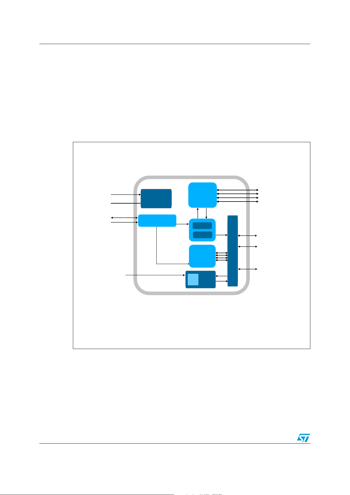
1 STMPE812A functional overview
The STMPE812A consists of the following blocks:
2
● I
C interface
● GPIO/PWM controller
● Touchscreen controller (TSC)
● Analog-to-digital converted (ADC)
● Driver and switch control unit
Figure 1. STMPE812A block diagram
Tou ch
VDD
GND
Power
Power
Management
Management
Tou ch
Screen
Screen
Drivers and
Drivers and
Switches
Switches
X+
X+
X-
XY+
Y+
Y-
Y-
SDA
SCL
2%3%4.
43#4OU CHSCREENCONTROLLER
!$#!NALOGTO
$IGITAL#ONVERTER
I2C InterfaceI2C Interface
TSC
TSCTSC
ADC
ADCADC
GPIO/PWM
GPIO/PWM
Controller
Controller
POR
PORPOR
Reset
Reset
System
System
M
U
X
'0)/!$#07-
'0)/!$$2
'0)/).4
!-6
4/53 Doc ID 18225 Rev 4
STMPE812A STMPE812A functional overview
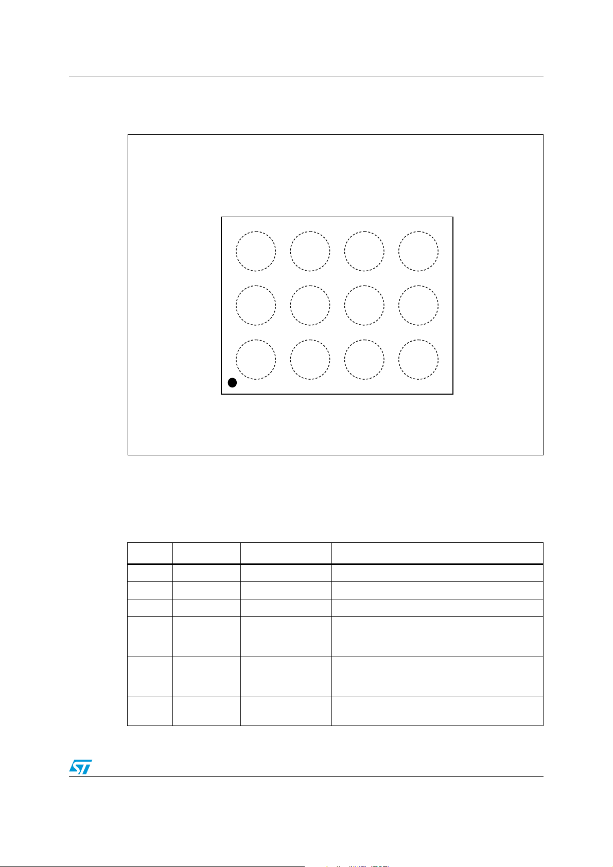
1.1 Pin configuration and functions
Figure 2. Pin configuration (top through view)
8
!
6##
!
0
!
Table 2. Pin assignments
9
"
0
"
0
"
8
#
2%3%4.
#
3$!
#
9
$
'.$
$
3#,
$
!-6
Pin Name Current capacity Function
B3 Y+ 50 mA current limit Y+
C3 X- 50 mA current limit X-
D3 Y- 50 mA current limit Y-
Active low RESET (3.6 V tolerant within VCC valid
range). Typical reset filter duration is 788 ns at
CC
.
1.8 V V
C2 RESETN
+8 mA/-12 mA at
3.3 V
Can be > 80 mA
D2 GND
load at touchscreen
Ground
and GPIO drive
2
C clock (fail safe, tolerant to 3.6 V regardless of
D1 SCL -4 mA
I
VCC)
Doc ID 18225 Rev 4 5/53

STMPE812A functional overview STMPE812A
Table 2. Pin assignments (continued)
Pin Name Current capacity Function
2
C data (fail safe, tolerant to 3.6 V regardless of
C1 SDA -4 mA
B1 P2
+8 mA/-12 mA at
3.3 V
I
)
V
CC
GPIO-2/ INT (3.6 V tolerant within V
range)
CC
valid
A1 P1
B2 P0
A2 V
CC
+8 mA/-12 mA at
3.3 V
+8 mA/-12 mA at
3.3 V
Can be > 80 mA
load at touchscreen
and GPIO drive
GPIO-1/ADC/PWM (3.6 V tolerant within V
range except VIN_ADC must be less than VCC)
GPIO-0/ADDR (3.6 V tolerant within V
range)
1.65 - 3.6 V core/IO supply (0.1 µF decoupling
cap)
No low-voltage detection for POR
20 µs POR from power stable
A3 X+ 50 mA current limit X+
Note: All I/O operates on VCC. All I/O tolerant up to 3.6 V, across VCC = 1.65 - 3.6 V
8 kV HBM ESD on all touchscreen pins (+/- 8 kV vs GND)
0.5 µA max input leakage as input, across V
range (GPIO, SCL/SDA)
CC
4 µs hardware filter on the 3 GPIOs as input
CC
CC
valid
valid
6/53 Doc ID 18225 Rev 4
STMPE812A STMPE812A functional overview
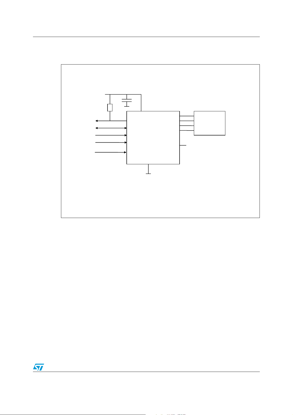
1.2 Typical application
Figure 3. Typical application
6
6##
).40
3#,
3$!
2%3%4.
!$$20
34-0%!
'.$
0
WIRE
RESISTIVE
TOUCHSCREEN
#ANBEUSEDAS!$#
07-OR'0)/
!-6
Doc ID 18225 Rev 4 7/53
I2C interface STMPE812A
2 I2C interface
For the bus master to communicate to the slave device, the bus master must initiate a Start
condition and be followed by the slave device address. Accompanying the slave device
address, there is a read/write bit (R/W). The bit is set to 1 for read and 0 for write operation.
If a match occurs on the slave device address, the corresponding device gives an
acknowledge on the SDA during the 9th bit time. If there is no match, it deselects itself from
the bus by not responding to the transaction.
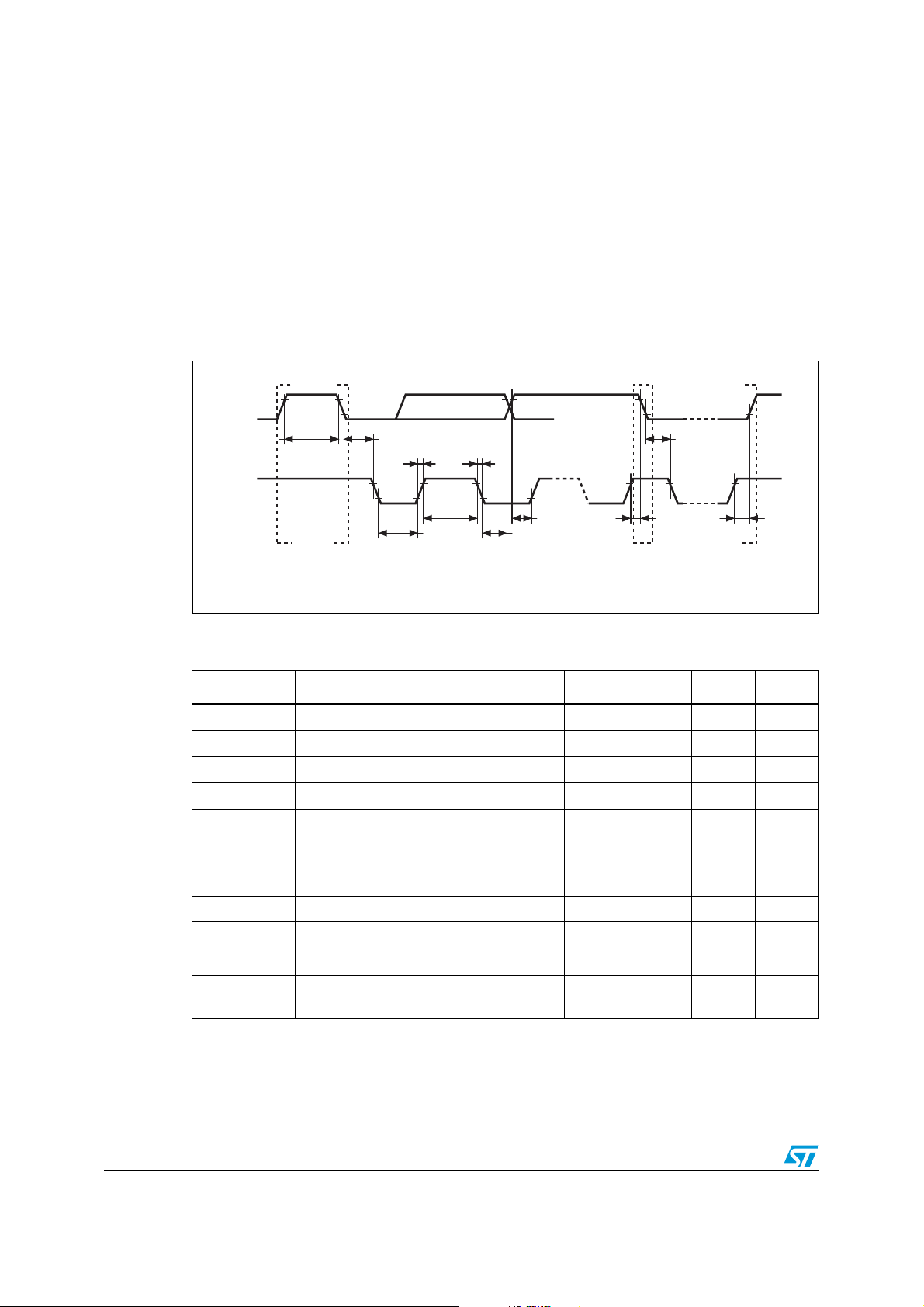
Figure 4. I
SDA
SCL
2
C timing diagram
tHD:STAtBUF
tR
SP
tHIGH
tLOW
tHD:STA
tF
tSU:DAT
tHD:DAT
SR
Table 3. I2C timing
Symbol Parameter Min Typ Max Unit
f
SCL
t
LOW
t
HIGH
t
F
t
HD:STA
SCL clock frequency 0 - 400 kHz
Clock low period 1.3 - - µs
Clock high period 600 - - ns
SDA and SCL fall time Note
START condition hold time (after this
period the first clock is generated)
(1)
- 300 ns
600 - - ns
tSU:STOtSU:STA
P
AI00589
t
SU:STA
t
SU:DAT
t
HD:DAT
t
SU:STO
t
BUF
1. Minimum TF is subject to system capacitive load (C
START condition setup time (only relevant
for a repeated start period)
Data setup time 100 - - ns
Data hold time 0 - - µs
STOP condition setup time 600 - - ns
Time the bus must be free before a new
transmission can start
LOAD
8/53 Doc ID 18225 Rev 4
600 - - ns
1.3 - - µs
) condition.
STMPE812A I2C interface
2.1 I2C features
The features that are supported by the I2C interface are listed below:
2
● I
C slave device
● Operates at V
● Compliant to Philips I
● Supports standard (up to 100 Kbps) and fast (up to 400 Kbps) modes
2
● I
C address in 0x41 (0x82/83 including Rd/Wr bit) or 0x40 (0x80/81 including Rd/Wr
bit)
The slave address is selected by the state of P0 pin. The state of the pin is read upon reset
and then the pin can be configured for normal operation. The pin shall have an external pullup or pull-down to set the address.
Table 4. Slave address
(1.65 V - 3.6 V)
CC
ADDR (P0) 7-bit I2C slave address
2
C specification version 2.1
040h
141h
Start condition
A Start condition is identified by a falling edge of SDATA while SCLK is stable at high state.
A Start condition must precede any data/command transfer. The device continuously
monitors for a Start condition and does not respond to any transaction unless one is
encountered.
Stop condition
A Stop condition is identified by a rising edge of SDATA while SCLK is stable at high state. A
Stop condition terminates communication between the slave device and the bus master. A
read command that is followed by NoAck can be followed by a Stop condition to force the
slave device into idle mode. When the slave device is in idle mode, it is ready to receive the
2
next I
C transaction. A Stop condition at the end of a write command stops the write
operation to registers.
Acknowledge bit
The acknowledge bit is used to indicate a successful byte transfer. The bus transmitter
releases the SDATA after sending eight bits of data. During the ninth bit, the receiver pulls
the SDATA low to acknowledge the receipt of the eight bits of data. The receiver may leave
the SDATA in high state if it does not acknowledge the receipt of the data.
2.2 Data input
The device samples the data input on SDATA on the rising edge of the SCLK. The SDATA
signal must be stable during the rising edge of SCLK and the SDATA signal must change
only when SCLK is driven low.
Doc ID 18225 Rev 4 9/53

I2C interface STMPE812A
Table 5. Operating modes
Mode Byte Programming sequence
Read ≥1
Write ≥1
Start, Device address, R/W
Restart, Device address, R/W
= 0, Register address to be read
= 1, Data Read, Stop
If no Stop is issued, the Data Read can be continuously performed. If
the register address falls within the range that allows an address autoincrement, then the register address auto-increments internally after
every byte of data being read. For register address that falls within a
non-incremental address range, the address is kept static throughout
the entire read operations. Refer to the memory map table for the
address ranges that are auto and non-increment.
Start, Device address, R/W
= 0, Register address to be written, Data
Write, Stop
If no Stop is issued, the Data Write can be continuously performed. If
the register address falls within the range that allows address autoincrement, then the register address auto-increments internally after
every byte of data being written in. For those register addresses that
fall within a non-incremental address range, the address is kept static
throughout the entire write operation. Refer to the memory map table
for the address ranges that are auto and non-increment.
10/53 Doc ID 18225 Rev 4
STMPE812A I2C interface
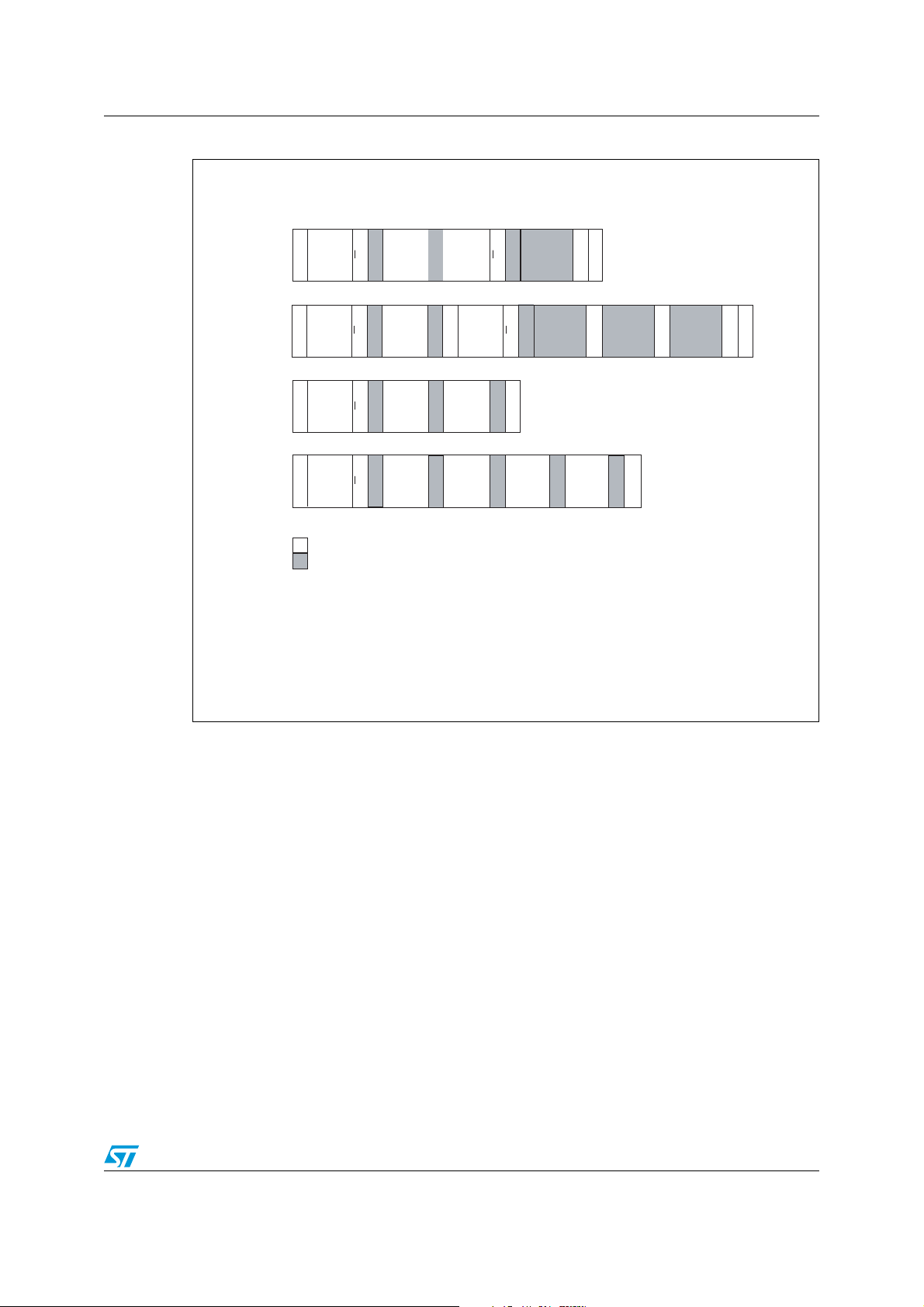
Figure 5. Read and write modes (random and sequential)
One byte
Read
More than one byte
More than one byte
Read
One byte
Write
Read
Start
Start
Start
Start
Device
Address
Device
Address
Device
Address
Device
Address
Master
Slave
R/W=0
R/W=0
R/W=0
R/W=0
Ack
Ack
Ack
Ack
Reg
Address
Reg
Address
Reg
Address
Reg
Address
Device
Ack
Address
Device
Ack
Address
Restart
Data
to be
Ack
written
R/W=1
Ack
Ack
R/W=1
Stop
Ack
Data
Read
Data
Read
Stop
No Ack
Ack
Data
Read + 1
Ack
Data
Read + 2
Stop
No Ack
Ack
Data to
Write
Data to
Ack
Write + 1
Ack
Write + 2
Data to
Ack
Stop
AM04175V1
Doc ID 18225 Rev 4 11/53

I2C interface STMPE812A
2.3 Read operation
A write is first performed to load the register address into the Address Counter but without
sending a Stop condition. Then, the bus master sends a reStart condition and repeats the
Device Address with the R/W bit set to 1. The slave device acknowledges and outputs the
content of the addressed byte. If no additional data is to be read, the bus master must not
acknowledge the byte and terminates the transfer with a Stop condition.
If the bus master acknowledges the data byte, then it can continue to perform the data
reading. To terminate the stream of data bytes, the bus master must not acknowledge the
last output byte, and be followed by a Stop condition. If the address of the register written
into the Address Counter falls within the range of addresses that has the auto-increment
function, the data being read is coming from consecutive addresses, which the internal
Address Counter automatically increments after each byte output. After the last memory
address, the Address Counter 'rolls-over' and the device continues to output data from the
memory address of 0x00. Similarly, for the register address that falls within a non-increment
range of addresses, the output data byte comes from the same address (which is the
address referred by the Address Counter).
Acknowledgement in read operation
For the above read command, the slave device waits, after each byte read, for an
acknowledgement during the ninth bit time. If the bus master does not drive the SDA to a
low state, then the slave device terminates and switches back to its idle mode, waiting for
the next command.
2.4 Write operations
A write is first performed to load the register address into the Address Counter without
sending a Stop condition. After the bus master receives an acknowledgement from the slave
device, it may start to send a data byte to the register (referred by the Address Counter).
The slave device again acknowledges and the bus master terminates the transfer with a
Stop condition.
If the bus master needs to write more data, it can continue the write operation without
issuing the Stop condition. Whether the Address Counter autoincrements or not after each
data byte write depends on the address of the register written into the Address Counter.
After the bus master writes the last data byte and the slave device acknowledges the receipt
of the last data, the bus master may terminate the write operation by sending a Stop
condition. When the Address Counter reaches the last memory address, it 'rolls-over' to the
next data byte write.
12/53 Doc ID 18225 Rev 4

STMPE812A Power supply
3 Power supply
The STMPE812A GPIO operates from a supply pin VCC. For better resolution and noise
immunity, V
Power up reset
The STMPE812A is equipped with an internal POR circuit that holds the device in reset
state, until the V
above 2.8 V is recommended.
CC
supply input is valid. The internal POR is tied to the VCC supply pin.
CC
Doc ID 18225 Rev 4 13/53

Charge pump STMPE812A
4 Charge pump
The STMPE812A is integrated with an internal charge-pump. The charge pump is required
for any ADC/TSC operations when V
Activating the charge pump when V
device.
is less than 2.5 V.
CC
> 2.5 V may result in permanent damage of the
CC
14/53 Doc ID 18225 Rev 4
STMPE812A Power modes
5 Power modes
The STMPE812A operates in a 2 states: active and hibernate.
Active:
– Whenever PEN-DOWN is detected, the device remains in active mode
– Whenever PWM is active, the device remains in active mode
– Whenever ADC is active, the device remains in ACTIVE MODE
Hibernate:
-PWM/ADC must be “off” (clock disable bit SET)
-Any GPIO input, with interrupt enabled, causes a transition to “active” state, if an input
change is detected.
-Pen down even causes transition to “active” state if the touchscreen controller is enabled.
Table 6. Power mode
Power mode Active Hibernate
Current consumption 280 µA (max)
GPIO hotkey Yes Yes
(1)
1.0 µA (max.)
Touchscreen Yes Yes
2
Interface (I
1. At Vcc=1.8V, TCS running at 100sets of X/Y per second, MAV disabled.
C) Yes Yes
Doc ID 18225 Rev 4 15/53
Power modes STMPE812A
Figure 6. Power modes state diagram
ACTIVE
Soft -Reset, Reset input
I2C activity,
No activity
(about 33 μs)
STMPE812A is in
active mode if PWM
is running
Touch, Hotkey
AUTO -
HIBERNATE
On power up reset, device goes to active state. However, as all the functional blocks are
clocked off by default, no touch/hotkey activity is possible. If there are no I
POR
Reset Input
2
C activities,
AM04141V1
device goes into auto-hibernate mode automatically.
The auto-hibernate feature of STMPE812A is always enabled. Whenever there is a period of
inactivity, the device enters this mode to reduce power consumption. On detection a touch,
correctly addressed I
2
C data, GPIO activity, the device wakes up immediately.
As the device is able to wake up very quickly, there is no loss of touch data.
16/53 Doc ID 18225 Rev 4

STMPE812A STMPE812A registers
6 STMPE812A registers
This section lists and describes the registers of the STMPE812A device, starting with a
register map and then provides detailed descriptions of register types.
Table 7. Register summary map table
Address Register name Bit Type Reset value Function
Registers from 0x00 - 0x0F are always accessible.
0x00 - 01 CHIP_ID 16 R 0xA812 Device identification
0x02 ID_VER 8 R 0x10
0x03 SYS_CTRL 8 R/W 0x0F System control register
0x04
0x06 - 07 SCRATCH_PAD 16 R/W 0x00
0x08 INT_CTRL 8 R/W 0x00 Interrupt control register
0x09 INT_EN 8 R/W 0x00 interrupt enable register
0x0A INT_STA 8 R 0x00 Interrupt status register
Registers from 0x10 - 0x1F are accessible only if “GPIO_OFF” bit in SYS_CTRL is set to “0”.
0x10 GPIO_SET_PIN 8 R/W 0x00 GPIO set pin register
0x11 GPIO_CLR_PIN 8 R/W 0x00 GPIO clear pin register
0x12 GPIO_MP_STA 8 R/W 0x00
0x13 GPIO_DIR 8 R/W 0x00
0x14 GPIO_ED 8 R/W 0x00
PORT_FUNCTI
ON
8 R/W 0xF8 Port function control register
Revision number
0x10 for engineering sample
General purpose storage
register
GPIO monitor pin state
register
GPIO falling edge register
GPIO rising edge register
Registers from 0x20 - 0x2F are accessible only if “ADC_OFF” bit in SYS_CTRL is set to “0”.
0x20 ADC_CTRL 8 R/W 0x33 ADC control
0x21 - 22 ADC_DATA 16 R 0x0000 ADC data
Registers from 0x40 - 0x4F are accessible only if “TSC_OFF” bit in SYS_CTRL is set to “0”.
0x40 TSC_CTRL 8 R/W 0x00
0x41
0x42
0x43
TSC_DET_CFG
1
TSC_DET_CFG
2
TSC_SAMPLIN
G_RATE
8R/W 0xA4
8R/W 0xB0
8R/W 0x0A
Doc ID 18225 Rev 4 17/53
4-wire touchscreen
controller setup
Touchscreen controller
configuration 1
Touchscreen controller
configuration 2
Touchscreen controller
sampling rate register

STMPE812A registers STMPE812A
Table 7. Register summary map table (continued)
Address Register name Bit Type Reset value Function
0x44 TSC_DATA 8 R - Non auto-increment address
Registers from 0x50 - 0x5F are accessible only if “PWM_OFF” bit in SYS_CTRL is set to “0”.
0x50
PWM_CLOCK_
DIV
8 R/W 0x00 PWM clock divider
0x51 PWM_CTRL1 8 R/W 0x00
6.1 Auto-increment/non auto-increment address
The STMPE812A supports auto-increment accesses on all, except for TSC data register
(0x44). While accessing auto-increment register location, consecutive read/write access
data from the consecutive registers. Note that for register accesses started on autoincremental addresses, the address 0x44 is skipped.
For example:
Write register address (0x40)
Read data (data of 0x40)
Read data (data of 0x41)
Read data (data of 0x42)
Read data (data of 0x43)
Read data (data of 0x45) <= 0x44 is skipped.
Master control of PWM
channel 1
18/53 Doc ID 18225 Rev 4

STMPE812A System and identification registers
7 System and identification registers
Table 8. System and identification registers map
Address Register name Bit Type Reset Function
0x00 - 01 CHIP_ID 16 R 0x0A812 Device identification
0x02 ID_VER 8 R 0x10
0x03 SYS_CTRL 8 R/W 0xF8 System control register
0x04 PORT_FUNCTION 8 R/W 0x00 Port function control register
0x06 - 07 SCRATCH_PAD 16 R/W 0x00
Revision number
0x10 for engineering sample
General purpose storage
register
SYS_CTRL System control register
76543 2 1 0
RESERVED SOFT_RESET TSC_EN RESERVED PWM_OFF GPIO_OFF TSC_OFF ADC_OFF
00001 1 1 1
Address: 0x03
Type: R/W
Reset: 0x0F
Description: System control register.
[7] RESERVED
[6] SOFT_RESET
Reset the 812 using serial communication
ALL REGISTER VALUES ARE RESET. State machines all back to POR states.
[5] TSC_EN
Write ‘1’ to enable operation of TSC. Write ‘0’ to disable it.
[4] RESERVED
[3] PWM_OFF
Writing ‘1’ switches OFF the clock supply to PWM
[2] GPIO_OFF
Writing ‘1’ switches OFF the clock supply to GPIO
[1] TSC_OFF
Writing ‘1’ switches OFF the clock supply to touchscreen controller
[0] ADC_OFF
Writing ‘1’ switches OFF the clock supply to ADC
If the clock supply to a particular functional block is turned off, the registers of these
modules are not accessible.
Doc ID 18225 Rev 4 19/53

System and identification registers STMPE812A
PORT_FUNCTION Port function control register
76543 2 1 0
PORT 2 FUNCTION RESERVED PORT 1 FUNCTION PORT 0 FUNCTION
11111 0 0 0
Address: 0x04
Type: R/W
Reset: 0xF8
Description: Port function control register.
[7:6] PORT 2 FUNCTION
[5:4] RESERVED
[3:2] PORT 1 FUNCTION
[1:0] PORT 0 FUNCTION
Port function:
'00' - GPIO input
'01' - GPIO output
'10' - ADC input (P1 only)
'11' - Special function
Special function for:
P0 - NONE
P1 - PWM
P2 - INT output
SCRATCH_PAD Scratch pad register
76543 2 1 0
SCRATCHPAD
00000 0 0 0
Address: 0x06 - 07
Type: R/W
Reset: 0x00
Description: General purpose scratch pad register. Could be used for testing of serial interface
reliability.
[15:0] SCRATCHPAD
20/53 Doc ID 18225 Rev 4

STMPE812A Interrupt system
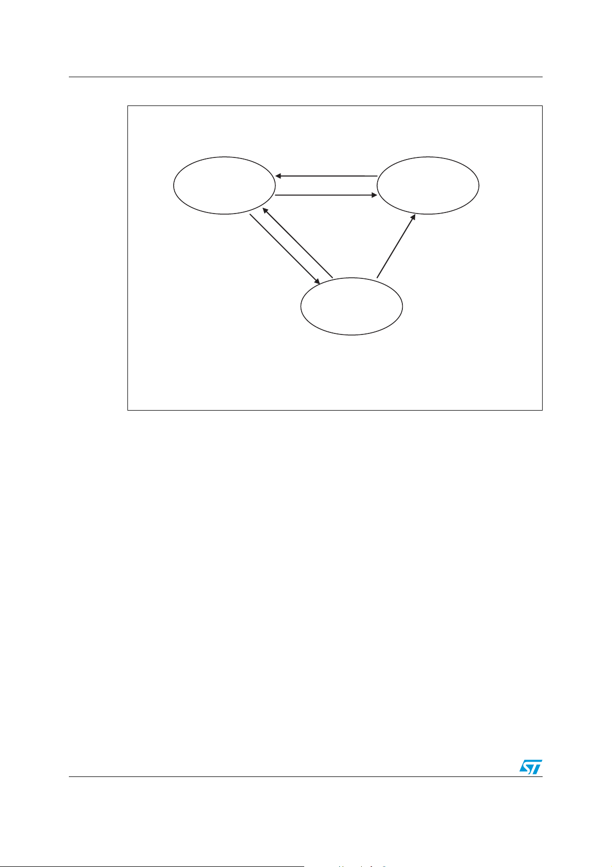
8 Interrupt system
The STMPE812A uses a 2-tier interrupt structure. In normal mode, interrupts from the GPIO
and touchscreen controller assert the INT pin and are available in the Interrupt Status
register (ISR).
In pen down mode, the INT pin is asserted as long as pen down is detected.
Since the INT pin is a OR function of the pen down and all other enabled interrupts, in order
for INT pin to provide the exclusive indication of pen down (INT = Low) and pen up
(INT = High), as such benefit from minimal I
down mode when the GPIO/PWM/ADC functions are not required or the GPIO/PWM/ADC
interrupts are disabled.
Figure 7. Interrupt system diagram
0%.$/7.-/$%
2
C transactions, it is recommended to use pen
4OUCHSCREENSTATUS
07-'0)/ACTIVITY
0%.$/7.
)NTERRUPT
STATUS
)
NTERRUPT
ENABLE
!.$
!.$
).4PIN
/2
!-6
Doc ID 18225 Rev 4 21/53

Interrupt system STMPE812A
INT_CTRL Interrupt control register
76543 2 1 0
INT_MODE RESERVED INT_POLARITY INT_TYPE GLOBAL_INT
0 0 000
Address: 0x08
Type: R/W
Reset: 0x00
Description: This register is used to enable the interruption from a system related interrupt source
to the host.
[7] INT_MODE:
‘0’ for Pen-Down INT mode (INT pin asserted as long as pen down detected). Nothing can deassert the INT pin as long as PEN is down. TSC_TOUCH in INT_EN register must be enabled
for PEN_DOWN interrupt to operate.
If any other interrupt sources are enabled, the INT output is:
PEN_STATUS OR OTHER_INT
INT_E setting is not required for PEN-DOWN mode. It is recommended Pen-Down INT mode
enabled in applications where GPIO/ADC/PWM functions or interrupts are not in used, such
that the INT pin signal provides the exclusive indication for pen down and pen up.
‘1’ for normal INT mode (INT pin asserted if any bit in INT STATUS REGISTER is set)
When INT_MODE is changed, all interrupt status are cleared. Pending INT output (if any) is
cleared too.
[6:3] RESERVED
[2] INT_ POLARITY:
‘1’ for active high/rising edge
‘0’ for active low/falling edge
Interrupt pin should be pulled to V
high” polarity is used.
[1] INT_TYPE:
‘1’ for edge interrupt (pulse width = 50-150 µs)
‘0’ for level interrupt
Edge interrupt does not work in PEN_DOWN INT mode
This bit is ignored in PEN_DOWN INT mode.
[0] GLOBAL_INT:
‘1’ allows global interrupt
‘0’ stops all interrupt
This bit overwrites INT_MODE: If global_int is stop (in pen down INT_MODE), even pen down
does not generate an interrupt.
if “active low” polarity is used, and pulled to GND if “active
CC
22/53 Doc ID 18225 Rev 4

STMPE812A Interrupt system
INT_EN Interrupt enable register
7 6 543 2 1 0
TSC_ERR TSC_RELEASE P2 RESERVED P1 P0 TSC_DATA TSC_TOUCH
0 0 000 0 0 0
Address: 0x09
Type: R/W
Reset: 0x00
Description: This register is used to enable the interruption from a system related interrupt source
to the host.
[7] TSC_ERR
Error encountered in coordinate calculation in touchscreen controller
[6] TSC_RELEASE:
Release of TSC is detected
[5] P2:
Port 2 activity (GPIO)
[4] RESERVED
[3] P1
Port 1 activity (GPIO/ADC/PWM)
[2] P0
Port 0 activity (GPIO)
[1] TSC_DATA
Touch data available
[0] TSC_TOUCH
Touch is detected
Note: * Hotkey interrupt should have respond time of <5 µs in active mode and less than 1 ms in
hibernate mode.
Doc ID 18225 Rev 4 23/53

Interrupt system STMPE812A
ISR Interrupt status register
7 6 543 2 1 0
TSC_ERR TSC_RELEASE P2 RESERVED P1 P0 TSC_DATA TSC_TOUCH
0 0 000 0 0 0
Address: 0x0A
Type: R
Reset: 0x00
Description: ISR register monitors the status of the interruption from a particular interrupt source
to the host. Regardless whether the INT_EN bits are enabled, the ISR bits are still
updated.
Writing to this register has no effect. Reading the register clears any asserted bit
Implementation: A shadow register MUST be used to ensure that Read+Clear action
DOES NOT clear up any bit that is not READ.
Note: Reading the Interrupt Enable Register also clears the ISR. It is recommended that no read operation on IER
to be executed during normal operation. IER should only be accessed during initialization.
[7] TSC_ERR
Error encountered in coordinate calculation in TSC, or touch detect not valid after sampling
[6] TSC_RELEASE:
Release of touch is detected
[5] P2
Port 2 activity (GPIO)
[4] RESERVED
[3] P1
Port 1 activity (GPIO/ADC/PWM)
[2] P0
Port 0 activity (GPIO)
[1] TSC_DATA
Touch data available. In internal timer and host-read controlled mode, this bit can only
be cleared after the data has been read by the host. In ACQ mode, this bit is cleared after the
data or the ISR is read by the host.
[0] TSC_TOUCH
Touch is detected.
(In PEN-DOWN interrupt mode, this bit is never cleared until pen is removed)
In PEN_DOWN interrupt mode, this status register will still be updated with event interrupt
status data, and cleared on read. However no interrupt will be issued based on this status
register.
24/53 Doc ID 18225 Rev 4

STMPE812A ADC controller
9 ADC controller
A 12-bit ADC is integrated in the STMPE812A. The ADC could be used as generic analogdigital converter, or a touchscreen controller capable of controlling a 4-wire resistive
touchscreen.
The ADC works ONLY with internal reference (equal to V
Table 9. ADC controller registers
Address Register name Bit Type Reset Description
0x20 ADC control 8 R/W 0x33 ADC control
0x21-0x22 ADC data 16 R 0x0000 ADC data access (P1)
), always 12 bit.
CC
Doc ID 18225 Rev 4 25/53

ADC controller STMPE812A
ADC control register ADC control
76543 2 1 0
ADC_MODE ADC_CAP ADC_FREQ CP_ARM CP_Lock[1:0] RESERVED
00110 0 1 1
Address: 0x20
Type: R/W
Reset: 0x33
Description: This register is used to configure the ADC operations.
[7] ADC_MODE: ADC capture mode
‘0’ – Continuous capture according to sampling rate specified by ADC_FREQ register. New
data over-writes old data in ADC_DATA register.
‘1’ – One-shot capture. One sample is taken every time system writes ‘1’ to ADC_CAP bit
[6] ADC_CAP: ADC channel data capture
In one-shot mode:
Write ‘1’ to initiate data acquisition for the corresponding channel. Writing ‘0’ has no effect.
Reads ‘1’ if conversion is in progress.Reads ‘0’ if conversion is completed.
One-shot mode ADC generates interrupt in corresponding interrupt status bit on completion of
conversion
In continuous capture mode:
Write ‘1’ to initiate data acquisition for the corresponding channel. Writing ‘0’ to stop capturing.
[5:4] ADC_FREQ: ADC sampling frequency based on 1MHz RC (minimum 880 KHz)
00 – 10 K samples/sec
01 – 12.5 K samples/sec
10 – 15 K samples/sec
11 – 20 K samples/sec
NOTE: As the ADC is also used for TSC operation. This setting affects the maximum sampling
rate possible with TSC.
[3] CP_Arm: Writing ‘1’ arms the charge-pump for unlocking
Writing ‘0’ un-arms it
Charge-pump is required for ADC/TSC operation when V
charge pump when V
is more than 2.5 V may result in permanent damage of the
CC
device.
Charge-pump can be activated by unlocking CP_Lock after it is armed.
[2:1] CP_Lock[1:0]: Only effective if CP_Arm is set to ‘1’.
Always reads ‘00’.
Writing ‘01’ when CP_Arm is ‘1’ activates the charge pump.
Writing ‘00’, ‘10’ and ‘11’ does NOT activate the charge-pump, and clears the CP_Arm bit.
CP_Arm MUST BE set before writing to CP_Lock. Accesses to CP_Lock will be ignored, if
CP_Arm is ‘0’.
Note: CP_Arm and CP_Lock CANNOT be accessed in a single I
first ARM the CP with 1 I
2
C transaction, and unlocks it in the next. CP_LOCK reads “00”
if charge pump is activated
CP_LOCK reads “01” if charge pump is not activated
is less than 2.5 V. Activating the
CC
2
C transaction. System must
[0] RESERVED
26/53 Doc ID 18225 Rev 4

STMPE812A ADC controller
ADC data ADC data register
76543 2 1 0
ADC_DATA_7 ADC_DATA_6 ADC_DATA_5 ADC_DATA_4 ADC_DATA_3 ADC_DATA_2 ADC_DATA_1 ADC_DATA_0
00000 0 0 0
Address: 0x21-0x22
Type: R
Reset: 0x0000
Address: ADC data register.
[7:0] ADC_DATAx
Note: When the I
guaranteed (once access starts, content will only be updated after BOTH bytes has been
read, OR I
- 0x21 is LSB
- 0x22 is MSB
2
C master accesses the data register, upper/lower byte consistency must be
2
C master accesses other register address):
Doc ID 18225 Rev 4 27/53

PWM controller STMPE812A
10 PWM controller
The PWM allows the brightness control of a LED/motor driver.
The PWM uses base clock that is ½ of the OSC frequency (typically 600 kHz). The base
clock is divided by a programmable DIV[4:0], which scales it to 18.75-600 kHz. This clock
goes into PWM controller and outputs a signal that is pulse-width modulated (16 steps), with
a frequency 16 times smaller.
10.1 Register map for PWM function
Table 10. PWM function registers
Address Register name Bit Type Reset Description
0x50 PWM_ClockDiv 8 R/W 0x00 PWM clock divider
0x51 PWM_Control_1 8 R/W 0x00
Master control of PWM channel 1
Output at port 0
PWM clock div register PWM clock divider register
76543 2 1 0
BurstLength [1:0] DIV[4:0]
00000 0 0 0
Address: 0x50
Type: R/W
Reset: 0x00
Description: PWM clock divider register.
[7:5] BurstLength[2:0]
Burst length of PWM output
‘000’ – 8 ms
‘001’ – 16 ms
‘010’ – 32 ms
‘011’ – 64 ms
‘100’ – 128 ms
‘101’ – 256 ms
‘110’ – 512 ms
‘111’ – 1024 ms
[4:0] Div[4:0]
PWM controller is based on 600KHz clock divided by (Div[4:0] + 1).
Effectively, PWM clock is:
600 KHz (MAX)
600 KHz/32 = 18.75 KHz (MIN)
28/53 Doc ID 18225 Rev 4

STMPE812A PWM controller
PWM control1 register PWM control1 register
76543 2 1 0
Brightness BurstMultiplier Off_State Enable
0000
Address: 0x51
Type: R/W
Reset: 0x00
Description: PWM control1 register.
[7:4] This defines the of the PWM channel output which in turn determines the brightness level of
the LED that the PWM output drives. Note that this is assuming LED is connected in SINKING
MODE. System host should program the brightness in a reverse way if sourcing configuration
were to be used.
0000: duty cycle ratio 1:15 (6.25%, minimum brightness)
0001: duty cycle ratio 2:14 (12.50%)
0010: duty cycle ratio 3:13 (18.75%)
0011: duty cycle ratio 4:12 (25.00%)
0100: duty cycle ratio 5:11 (31.25%)
0101: duty cycle ratio 6:10 (37.50%)
0110: duty cycle ratio 7: 9 (43.75%)
0111: duty cycle ratio 8: 8 (50.00%)
1000: duty cycle ratio 9: 7 (56.25%)
1001: duty cycle ratio 10: 6 (62.50%)
1010: duty cycle ratio 11: 5 (68.75%)
1011: duty cycle ratio 12: 4 (75.00%)
1100: duty cycle ratio 13: 3 (81.25%)
1101: duty cycle ratio 14: 2 (87.50%)
1110: duty cycle ratio 15: 1 (93.75%)
1111: duty cycle ratio 16: 0 (100.00%, maximum brightness)
[3:2] BurstMultiplier
PWM output continues for time = BurstLength * BurstMultiplier
*If BurstMultiplier = 0, PWM output indefinitely (until PWM is turned OFF)
1 Off_State
‘0’ : PWM Output “HI” when PWM not running
‘1’ : PWM Output “LOW” when PWM not running
0Enable
Writing ‘1’ to this bit starts the PWM controller sequence
Writing ‘0’ has stops it
Reads ‘1’ when PWM is running.
Doc ID 18225 Rev 4 29/53

PWM controller STMPE812A
10.2 Interrupt of PWM controller
When non-infinite sequence is used, the completion of the PWM sequence causes the P0
bit in interrupt status register to be asserted.
30/53 Doc ID 18225 Rev 4

STMPE812A Touchscreen controller
11 Touchscreen controller
The STMPE812A is integrated with a hard-wired touchscreen controller for 4-wire resistive
type touchscreen. The touchscreen controller is able to operate completely autonomously,
and would interrupt the connected CPU only when pre-defined event occurs.
The TSC is based on an internal 20Ksamples/sec ADC, running off a 1 MHz (minimum
880 kHz) RC OSC.
Sampling time = touch detect delay*2 + (settling time + (ADC conversion time*MAV) ) *3
Table 11. Sampling time/frequency calculation
ADC
Oscillator speed
conversion
time
880kHz 50µs 40µs 40µs None
Tou ch
detect
delay
Settling
time
Median
average
(complete X/Y/Z sample
40*2 + 3*(40+(50*1)) = 350 µs
(2.8K sample sets/sec)
40*2 + 3*(40+
880kHz 50µs 40µs 40µs 10-2
(50*10))=1700 µs (588 sample
sets/sec)
640*2 + 3*(640+ (50*20))
880 kHz 50 µs 640 µs 640 µs 20-4
=6200 µs (161 sample
sets/sec)
Figure 8. Touchscreen controller internal RC OSC connection
-(Z
MINIMUM+
2#/3#
BITCH!$#
MAX
+SAMPLESSAT-(Z
Sampling time/freq
sets)
43#TIMINGGENERATOR
43#SAMPLINGRATE
MSMS
!-6
Doc ID 18225 Rev 4 31/53

Touchscreen controller STMPE812A
11.1 Touchscreen controller detection sequence
Following is the sequence of detection in the STMPE812A touchscreen controller for X, Y
and Z:
1. Touch detect
2. Drive Y
3. Wait for settling time
4. Measure Y
5. Stop drive
6. Drive Z
7. Wait for settling time
8. Measure Z
9. Stop drive
10. Drive X
11. Wait for settling time
12. Measure X
13. Stop drive
14. Touch detect
11.2 3 modes of acquisition
1. Data acquisition timed by internal timer:
The host system selects a “sampling period” with, based on internal timer, the touchscreen
controller takes a complete set of samples on every period. The host system may choose to
read the data by:
– Waiting for the INT
– Polling for INT_STATUS register for TOUCH DATA
– Reading the TSC_DATA at approximately the same timing. (Use “Data Valid Status
Read” option in this mode)
2. Data acquisition triggered by a write to “ACQ” bit:
As and when sampling is desired, host writes to the ACQ bit and:
– Poll the ACQ to wait for completion
– Wait for INT for Touch Data access
– Poll the FIFO after approximate time required for sampling. (Use “Data Valid
Status Read” option in this mode)
3. Data acquisition using host-controlled sampling rate control
The host sets the internal timer for the desired data-rate. On staring the touchscreen
controller in this mode, a complete set of sample is taken immediately. The touchscreen
controller enters in hibernate mode (clock is turned OFF, only monitors the PEN-DOWN
status). When system host reads the Touch Data available in FIFO, another set of data is
taken immediately.
32/53 Doc ID 18225 Rev 4

STMPE812A Touchscreen controller
11.3 Touchscreen controller registers
Table 12. Touchscreen controller registers
Address Register name Bit Type Reset Function
0x40 TSC_CTRL 8 R/W 0x00 Touchscreen control
0x41 TSC_DET_CFG1 8 R/W 0xA4 Touchscreen detection config 1
0x42 TSC_DET_CFG2 8 R/W 0xB0 Touchscreen detection config 2
0x43
0x44 TSC_DATA 8 R - Touchscreen data
TSC_SAMPLING
_RATE
8 R/W 0x0A Touchscreen sampling rate
Doc ID 18225 Rev 4 33/53

Touchscreen controller STMPE812A
TSC CTRL TSC control register
76543 2 1 0
MAV_MODE[2:0] ACQ Precharge[1:0] Current Limit [1:0]
000 0
Address: 0x40
Type: R/W
Reset: 0x00
Description: Touchscreen control register.
[7:5] MAV_MODE[2:0]
‘000’ – MAV filter disabled
‘001’ – 6 remove 2
‘010’ – 8 remove 4
‘011’ – 10 remove 2
‘100’ – 12 remove 4
‘101’ – 20 remove 4
‘110’ – 4 remove none (equal to 4 x oversampling)
‘111’ – 8 remove none (equal to 8 x oversampling)
[4] ACQ
Only valid in acquisition mode ‘01’ (acquisition initiated by system host writing to ACQ bit)
Writing ‘1’ to this bit initiates a TSC data acquisition
Writing ‘0’ has no effect
Reads ‘1’ if data acquisition is in progress
Reads ‘0’ if data is ready
If Data is already available in buffer and not read by system host, setting this bit to ‘1’ renders
the data in buffer “invalid”. DATA available bit in Interrupt Status register is reset by hardware
automatically. Pending interrupt due to DATA available (if any) is cleared.
Data pointer in multi-byte read operation is reset when this bit is written to.
[3:2] Precharge[1:0]
Pre-charge driver for touch detection
‘00’ – no pre-charge
‘01’ – 2 µs pre-charge
‘10’ – 4 µs pre-charge
‘11’ – 8 µs pre-charge
[1:0] Current Limit [1:0]
Current limit of touchscreen driver
‘00’ – 5 mA
‘01’ – 10 mA
‘10’ – 20 mA
‘11’ – 30 mA
34/53 Doc ID 18225 Rev 4

STMPE812A Touchscreen controller
TSC detect config TSC detection configuration 1 register
76543 2 1 0
PenStrength[1:0] TDetDly[2:0] Settling[2:0]
10100 1 0 0
Address: 0x41
Type: R/W
Reset: 0xA4
Description: Touchscreen controller detection configuration 1 register.
[7:6] PenStrength[1:0]
Pen detect strength threshold
‘00’ – least sensitive (50 K pull-up)
‘01’ – sensitive (40 K pull-up)
‘10’ – more sensitive (30 K pull-up) - Default
‘11’ – most sensitive (20 K pull-up)
[5:3] TDetDly[2:0]
Touch detect delay
‘000’ = 40 µs
‘001’ = 80 µs
‘010’ = 160 µs
‘011’ = 320 µs
‘100’ = 640 µs - Default
‘101’ = 1.28 ms
‘110’ = 2.56 ms
‘111’ = 5.12 ms
[2:0] Settling[2:0]
Panel driver settling time
‘000’ = 40 µs
‘001’ = 80 µs
‘010’ = 160 µs
‘011’ = 320 µs/ns
‘100’ = 640 µs - Default
‘101’ = 1.28 ms
‘110’ = 2.56 ms
‘111’ = 5.12 ms
For large panels (> 6 inches), a capacitor of 10 nF is recommended at the touchscreen
terminals for noise filtering. In this case, settling time of 1 ms or more is recommended.
Doc ID 18225 Rev 4 35/53

Touchscreen controller STMPE812A
TSC_DET_CFG2 TSC detection configuration 2 register
76543 2 1 0
Acq_Mode StatusRead OpMode Z-Divider[3:0]
10110 0 0 0
Address: 0x42
Type: R/W
Reset: 0xB0
Description: Touchscreen controller detection configuration 2 register.
[7:6] Acq_Mode
‘00’ – Data acquisition timed by internal timer
‘01’ – Data acquisition triggered by a write to “ACQ” bit
‘10’ – Data acquisition using Host-Controlled Sampling Rate Control. (Default)
‘11’ – Reserved
In mode ‘10’, device sample a complete data set every time host accesses the buffer. After
completion of sampling, device enters hibernate mode, until data is accessed again. (Or PENUP causing interrupt to de-assert)
[5] StatusRead
‘1’ inserts data valid (data available) status read in data port. (Default)
Reading data port in this mode clears the ISR register (equivalent to accessing interrupt status
register)
‘0’ – no data valid (data available) status access by data port
[4] OpMode
TSC operating mode
‘0’ for 12-bit X,12-bit Y,8-bit Z acquisition
‘1’ for 12-bit X, 12-bit Y only (Default)
This field cannot be written on, when EN=1
[3:0] Z-Divider[3:0]
Pen-Pressure is internally calculated as a 16-bit integer. As 16-bit resolution is typically not
required for touchscreen operation, STMPE812A right-shifts the value internally by ZDivider[3:0].
Z-value read through the TSC Data register is the lowest 8-bit of the shifted value.
36/53 Doc ID 18225 Rev 4

STMPE812A Touchscreen controller
TSC sampling rate TSC sampling rate register
76543 2 1 0
SAMPLING
00001 0 1 0
Address: 0x43
Type: R/W
Reset: 0x0A
Description: Touchscreen controller sampling rate control register.
[7:0] Sampling[7:0]
Sets the sampling rate of touchscreen controller.
Sampling Time = (sampling[7:0]+1) in ms
Clock cycle = 1 µs (1 MHz RC OSC)
Sampling time = 1 ms – 256 ms
NOTE:
This is used as “TSC regular initiator signal’. As long as there remains a valid touch, every
interval of this timing, the touchscreen controller executes a complete drive/settling/multisample/MAV/data calculation. It is the user’s responsibility to choose a sampling time that is
enough, based on ADC_FREQ, settling time and filter.
TSC_data Touchscreen data register
76543 2 1 0
TSC_DATA_7 TSC_DATA_6 TSC_DATA_5 TSC_DATA_4 TSC_DATA_3 TSC_DATA_2 TSC_DATA_1 TSC_DATA_0
00000 0 0 0
Address: 0x42
Type: R/W
Reset: 0xB0
Description: The data format of the touchscreen controller data register depends on the setting of
“OpMode” field in the touchscreen detection configuration 2 register. The samples
acquired are accessed in “packed samples”. The size of each “packed sample”
depends on which mode the touchscreen controller is operating in.
[7:0] TSC_DATA_x: Data byte from touchscreen controller.
Note: In order to preserve the integrity of the data, it is mandatory to ensure the following:
- System host to read exactly the number of bytes according to the programmed operating
mode
- I2C host to insert a STOP condition after each data read command
Data pointer in this 1-level buffer could be reset by:
-User issued ACQ in user initiated acquisition mode. In mode ‘10’, every time sampling is
completed, it overwrites the buffer, and reset the data pointer
Doc ID 18225 Rev 4 37/53

Touchscreen controller STMPE812A
Table 13. Touchscreen controller data register
TSCDetectConfig2
OpMode StatusRead
0 0 4 [11:4] of X
1 0 3 [11:4] of X
01 5
11 4
Number of
bytes to read
from
TSCData
Byte0 Byte1 Byte2 Byte3 Byte4
Data Valid
Status
Data Valid
Status
[3:0] of X
[11:8] of Y
[3:0] of X
[11:8] of Y
[11:4] of X
[11:4] of X
[7:0] of Y [7:0] of Z
[7:0] of Y -
[3:0] of X
[11:8] of Y
[3:0] of X
[11:8] of Y
[7:0] of Y [7:0] of Z
[7:0] of Y -
Data Valid Status Byte Structure
76543 2 1 0
RESERVED DATA VALID RESERVED
[7:2] RESERVED
[1] DATA VALID
1: Touch data available/valid
0: Touch data not available/not valid
Bit reset upon read
[0] RESERVED
Data Valid Status Read in data port is useful together with Pen Down mode whereby
accessing the ISR is not needed so as to achieve the best I
minimal I
2
C transactions).
Note: Reading the Data valid Status byte also clears the ISR.
2
C bandwidth efficiency (i.e.
38/53 Doc ID 18225 Rev 4

STMPE812A Touchscreen controller
11.4 Programming model
Below are steps to configure the Touchscreen controller in 3 different acquisition modes.
A. Autonomous touchscreen controller, 100 Hz, lowest power possible
1. Initialize the touchscreen controller (choose ACQ_Mode ‘00’ - data acquisition timed by
internal timer)
2. Initialize interrupt (with TSC_Data enabled, normal interrupt mode)
3. Wait for interrupt
4. On interrupt: Read interrupt status (this clears the set bits too)
5. If data is available, read data.
Note: If one set of data is available in buffer, and not accessed by the I
timer is up for the next data, the STMPE812A samples the next data as scheduled.
If old data is still NOT accessed when new data is ready to be written to the buffer, it is overwritten.
If old data is IN PROGRESS of being accessed, new data is DISCARDED.
2
If I
C host accessed PART OF the data, and moved on to read ANY OTHER REGISTER
LOCATION, the existing data is CONSIDERED READ, and new data ready to be written into
buffer
B. Non-autonomous touchscreen controller style-interrupt, 100Hz, lowest
power possible:
1. Initialize TSC (Choose ACQ_Mode ‘01’ - Data acquisition triggered by a write to “ACQ”
bit)
2. Initialize Interrupt (With TSC_Data, TSC_Touch enabled, PEN_DOWN interrupt mode)
3. Wait for Interrupt
4. On Interrupt: Read Interrupt Status (this clears the set bits too)
5. If PEN_DOWN, start SYSTEM_TIMER (10 ms typically)
6. On TIMEOUT, write ACQ bit to start acquisition
7. Poll interrupt status register or ACQ bit to check for acquisition status
8. ON issuing ACQ, 812 may assume that data in buffer is already accessed by I2C host,
and reset the relevant pointers.
2
C host, yet the sampling
C. Host-controlled sampling rate (lowest bus utilization)
1. Initialize TSC (choose ACQ_Mode ‘10’ - Data acquisition using host-controlled
sampling rate control)
2. Initialize interrupt (with TSC_Data, TSC_Touch enabled, PEN_DOWN interrupt mode)
3. Wait for Interrupt
4. On interrupt: Read Interrupt Status (this clears the set bits too)
5. If PEN_DOWN, start SYSTEM_TIMER (10 ms typically)
6. On TIMEOUT, read data
Doc ID 18225 Rev 4 39/53

Touchscreen controller STMPE812A
The STMPE812A samples a new data set immediately after every complete read.
If the host does not complete a data-set read, no further samples are taken.
For each data point (4 bytes), number of I2C transaction required is:
A: read Data Valid Status (1 byte), read data (4 bytes)
B: write ACQ (1 byte), read ACQ (1 byte), read data (4 bytes)
C: read (4 bytes)
40/53 Doc ID 18225 Rev 4

STMPE812A GPIO port controller
12 GPIO port controller
A total of 3 configurable ports are available in the STMPE812A port expander device.
If configured as GPIO input/output, they are controlled by the GPIO registers.
Table 14. GPIO registers
Address Register Bit Type Reset Function
0x10 GPIO_SET_PIN 8 R/W 0x00 Set pin state
0x11 GPIO_CLR_PIN 8 R/W 0x00 Clear pin state
0x12 GPIO_MP_STA 8 R/W 0x00 Monitor pin state
0x13 GPIO_DIR 8 R/W 0x00
0x14 GPIO_ED 8 R/W 0x00
All GPIO registers are named as GPxx, where:
Xxx represents the functional group
Falling edge
detection enable
Rising edge
detection enable
Bit76543210
GPxx IO-2 RESERVED IO-1 IO-0
The function of each bit is shown in Tab l e 1 5:
Table 15. GPIO registers
Register name Function
GPIO monitor pin state Reading this bit yields the current state of the bit. Writing has no effect.
Writing ‘1’ to this bit causes the corresponding GPIO to go to ‘1’ state.
GPIO set pin state
GPIO clear pin state
GPIO falling edge detection
enable
GPIO rising edge detection
enable
Writing ‘0’ to this bit has no effect
Reading this register always yield 0x00
Writing ‘1’ to this bit causes the corresponding GPIO to go to ‘0’ state.
Writing ‘0’ to this bit has no effect
Reading this register always yield 0x00
Writing ‘1’ to this bit allows interrupt generation when there is a falling
edge at the corresponding GPIO
Writing ‘0’ disables the interrupt generation on falling edge detection
Writing ‘1’ to this bit allows interrupt generation when there is a rising
edge at the corresponding GPIO
Writing ‘0’ disables the interrupt generation on rising edge detection
If both GPFE and GPRE are not set, state transition on a GPIO does not cause an interrupt.
On power-up reset, all GPIO are set as input.
Doc ID 18225 Rev 4 41/53

Electrical specification STMPE812A
13 Electrical specification
Table 16. Absolute maximum rating
Symbol Ratings Maximum value Unit
V
CC
Vi-i2c Input voltage at SDA/SCL 4.5 V
Vi-io Input voltage at P0-P5 4.5 V
ESD
Supply voltage 4.5 V
On all touchscreen and GPIO pins (HBM) ±8 kV
On all other pins (HBM) ±2 kV
Table 17. Thermal data
Symbol Parameter Value Unit
T
J
T Operating temperature -40°C-85°C °C
T
STG
Thermal resistance junction-ambient
(CSP 12)
Storage temperature -65°C-125°C °C
13.1 DC electrical characteristics
Table 18. Power consumption (T
Symbol Parameter Test conditions Min Typ Max Unit
amb
68 °C / W
= -40 °C to 85 °C)
V
=1.8V
CC
TSC running at 100 sets
of X/Y per second
max Operating current
I
CC
max Operating current
I
CC
42/53 Doc ID 18225 Rev 4
MAV disabled
Vcc=1.8V
TSC Running at 100 sets
of X/Y per second
MAV 6 remove 2
V
=3.3V
CC
TSC running at 100 sets
of X/Y/Z per second
MAV 10 remove 2
Vcc=1.8 V
TSC running at 100 sets
of X/Y/Z per second
MAV 10 remove 2
– 100 120
µA
– 230 280
– 670 810
µA
– 470 570

STMPE812A Electrical specification
Table 18. Power consumption (T
= -40 °C to 85 °C) (continued)
amb
Symbol Parameter Test conditions Min Typ Max Unit
VCC=1.8V
ICC max Operating current
TSC running at 100 sets
of X/Y/Z per second
– 870 1050 µA
MAV 20 remove 4
VCC=3.3V
I
max Operating current
CC
TSC running at 100 sets
of X/Y/Z per second
– 1190 1430 µA
MAV 20 remove 4
I
CC
suspend
Suspend current
No I2C/ADC activity
V
= 1.8 V - 3.3 V
CC
–0.5 1µA
*operating current excludes current driving the touchscreen.
(-40 °C to 85 °C. All GPIO complies to JEDEC standard JESD-8-7)
Table 19. DC electrical characteristics
Symbol Parameter Test conditions Min Typ Max Unit
V
CC
V
V
V
Core supply voltage 1.65 - 3.6 V
Input voltage low state VCC= 1.65 - 3.6 V -0.3 –
IL
IH
OL
Input voltage high
Output voltage low
state
state
= 1.65 - 3.6 V 0.80 V
V
CC
=3.6V,
V
CC
IOL=12mA
CC
-0.3 –
–VCC+0.3 V
0.20 V
C
0.45
C
V
V
V
OH
I
leakage
Output voltage high
state
All input pins except for
touchscreen I/O and
P0/P1
Doc ID 18225 Rev 4 43/53
=1.65 V,
V
CC
IOH=8 mA
= 1.65 V, VIN3.6 V – 0.1 0.5 µA
V
CC
0.85 V
CC
–VCC+0.3 V

Electrical specification STMPE812A
13.2 AC electrical characteristics
Table 20. AC electrical characteristics (-40 °C to 85 °C)
Symbol Parameter Test conditions Min Typ Max Unit
Max
ClkI2C
T
RESET
2
C maximum SCLK VCC=1.65-3.6V – – 400 KHz
I
Minimum RESET pulse
width
4– –µS
Minimum INPUT width
T
required for GPIO state
IN
4– –µS
transition
F
osc
Table 21. ADC specification
Internal RC OSC
frequency
= 1.65 - 3.6 V 900 1200 1500 KHz
V
CC
Parameter Test conditions Min Typ Max Unit
Full-scale input span 0 – V
Absolute input range -0.2 –
CC
+0.
V
CC
2
Input capacitance – 25 – pF
Leakage current – 0.1 – µA
Resolution – 12 – Bits
No missing codes 11 – – Bits
Integral linearity error – ±4 – LSB
V
V
Offset error – ±5 ±5 LSB
Gain error – ±14 ±18 LSB
Throughput rate – 180 – Ksamples/s
Table 22. Switch drivers specification
Parameter Test conditions Min Typ Max Unit
ON resistance X+, Y+
ON resistance X-, Y-
ON resistance X+, Y+
ON resistance X-, Y-
ON resistance X+, Y+
ON resistance X-, Y-
ON resistance X+, Y+
ON resistance X-, Y-
ON resistance X+, Y+
ON resistance X-, Y-
44/53 Doc ID 18225 Rev 4
V
= 1.65 V,
DD
5 mA setting
V
= 1.65 V,
DD
10 mA setting
= 1.65 V,
V
DD
20 mA setting
= 1.65 V,
V
DD
30 mA setting
V
=3.6V,
DD
5 mA setting
–34 – Ω
–24 – Ω
–17 – Ω
–15 – Ω
–31 – Ω

STMPE812A Electrical specification
Table 22. Switch drivers specification (continued) (continued)
Parameter Test conditions Min Typ Max Unit
ON resistance X+, Y+
ON resistance X-, Y-
ON resistance X+, Y+
ON resistance X-, Y-
ON resistance X+, Y+
ON resistance X-, Y-
Drive current (at 5 mA limit)
Drive current (at 10 mA
limit)
Drive current (at 20 mA
limit)
Drive current (at 30 mA
limit)
Drive current (at 5 mA limit)
Drive current (at 10 mA
limit)
VDD = 3.6 V,
10mA setting
VDD = 3.6 V,
20 mA setting
VDD = 3.6 V,
30 mA setting
=1.65 V
V
DD
X+/X- or Y+/Yshorted together
externally
=1.65 V
V
DD
X+/X- or Y+/Yshorted together
externally
=1.65 V
V
DD
X+/X- or Y+/Yshorted together
externally
=1.65V
V
DD
X+/X- or Y+/Yshorted together
externally
V
=3.6V
DD
X+/X- or Y+/Yshorted together
externally
=3.6V
V
DD
X+/X- or Y+/Yshorted together
externally
–22 – Ω
–16 – Ω
–14 – Ω
5mA
10 mA
19 mA
28 mA
7mA
13 mA
Drive current (at 20 mA
limit)
Drive current (at 30 mA
limit)
=3.6V
V
DD
X+/X- or Y+/Yshorted together
25 mA
externally
=3.6V
V
DD
X+/X- or Y+/Yshorted together
36 mA
externally
Doc ID 18225 Rev 4 45/53

Package mechanical section STMPE812A
14 Package mechanical section
In order to meet environmental requirements, ST offers these devices in different grades of
ECOPACK
specifications, grade definitions and product status are available at: www.st.com.
ECOPACK
Figure 9. Package outline for CSP 12 (2.17 x 1.67 mm)
®
packages, depending on their level of environmental compliance. ECOPACK®
®
is an ST trademark.
46/53 Doc ID 18225 Rev 4

STMPE812A Package mechanical section
Table 23. CSP 12 (2.17 x 1.67 mm) mechanical data
Symbol
Min Typ Max
A 0.585 0.650 0.715
A1 0.21 0.25 0.29
A2–0.35–
b 0.265 0.315 0.365
D 2.122.172.22
D1 – 1.5 –
E 1.621.671.72
E1 – 1.0 –
e0.450.50.55
fD – 0.335 –
fE – 0.335 –
SD–0.25–
ccc – 0.08 –
$ – 0.05 –
Millimeters
Doc ID 18225 Rev 4 47/53

Package mechanical section STMPE812A
Figure 10. Footprint recommendation
Figure 11. Tape information
48/53 Doc ID 18225 Rev 4

STMPE812A Package mechanical section
Table 24. Tape specifications
Symbol
Min Typ Max
Ao 1.78 1.83 1.88
Bo 2.34 2.29 2.34
Ko 0.68 0.73 0.78
F 3.453.503.55
E 1.651.751.85
W7.908.008.30
P2 1.95 2.00 2.05
Po 3.90 4.00 4.10
10Po 39.80 40.00 40.20
Do 1.50 1.55 1.60
T 0.185 0.200 0.215
P 3.904.004.10
Millimeters
Figure 12. Tape orientation
User direction of feed
1. Pin A1 is at top left corner based on above tape orientation.
AM00745V1
Doc ID 18225 Rev 4 49/53

Package mechanical section STMPE812A
Figure 13. Device marking
)DENTIFICATIONFOR
DEVICEFRONTEND
ANDBACKENDPLANT
Figure 14. Reel drawing (front)
6-.
977
'
)DENTIFICATIONFOR
(ALOGENFREE
)DENTIFICATIONFOR
TRACEABLEDATECODE
!-6
50/53 Doc ID 18225 Rev 4

STMPE812A Package mechanical section
Figure 15. Reel drawing (back)
Table 25. Tape width (millimeters)
A N W1 W2 W3
Tape width
max min max max min max
8 180 60 8,4 14.4 7.9 10.9
Doc ID 18225 Rev 4 51/53

Revision history STMPE812A
15 Revision history
Table 26. Document revision history
Date Revision Changes
18-Nov-2010 1 Initial release.
09-Mar-2011 2
23-May-2011 3
14-Jul-2011 4
Document status promoted from preliminary data to datatasheet.
Updated Ta bl e 2 .
Updated: Footprint recommendation in Figure 10. and Ta bl e 2 2
Replaced: Flip-chip 12 with CSP 12.
Updated: features description, title and template.
Modified: Table 3: I2C timing and Section 13: Electrical specification.
52/53 Doc ID 18225 Rev 4

STMPE812A
Please Read Carefully:
Information in this document is provided solely in connection with ST products. STMicroelectronics NV and its subsidiaries (“ST”) reserve the
right to make changes, corrections, modifications or improvements, to this document, and the products and services described herein at any
time, without notice.
All ST products are sold pursuant to ST’s terms and conditions of sale.
Purchasers are solely responsible for the choice, selection and use of the ST products and services described herein, and ST assumes no
liability whatsoever relating to the choice, selection or use of the ST products and services described herein.
No license, express or implied, by estoppel or otherwise, to any intellectual property rights is granted under this document. If any part of this
document refers to any third party products or services it shall not be deemed a license grant by ST for the use of such third party products
or services, or any intellectual property contained therein or considered as a warranty covering the use in any manner whatsoever of such
third party products or services or any intellectual property contained therein.
UNLESS OTHERWISE SET FORTH IN ST’S TERMS AND CONDITIONS OF SALE ST DISCLAIMS ANY EXPRESS OR IMPLIED
WARRANTY WITH RESPECT TO THE USE AND/OR SALE OF ST PRODUCTS INCLUDING WITHOUT LIMITATION IMPLIED
WARRANTIES OF MERCHANTABILITY, FITNESS FOR A PARTICULAR PURPOSE (AND THEIR EQUIVALENTS UNDER THE LAWS
OF ANY JURISDICTION), OR INFRINGEMENT OF ANY PATENT, COPYRIGHT OR OTHER INTELLECTUAL PROPERTY RIGHT.
UNLESS EXPRESSLY APPROVED IN WRITING BY TWO AUTHORIZED ST REPRESENTATIVES, ST PRODUCTS ARE NOT
RECOMMENDED, AUTHORIZED OR WARRANTED FOR USE IN MILITARY, AIR CRAFT, SPACE, LIFE SAVING, OR LIFE SUSTAINING
APPLICATIONS, NOR IN PRODUCTS OR SYSTEMS WHERE FAILURE OR MALFUNCTION MAY RESULT IN PERSONAL INJURY,
DEATH, OR SEVERE PROPERTY OR ENVIRONMENTAL DAMAGE. ST PRODUCTS WHICH ARE NOT SPECIFIED AS "AUTOMOTIVE
GRADE" MAY ONLY BE USED IN AUTOMOTIVE APPLICATIONS AT USER’S OWN RISK.
Resale of ST products with provisions different from the statements and/or technical features set forth in this document shall immediately void
any warranty granted by ST for the ST product or service described herein and shall not create or extend in any manner whatsoever, any
liability of ST.
ST and the ST logo are trademarks or registered trademarks of ST in various countries.
Information in this document supersedes and replaces all information previously supplied.
The ST logo is a registered trademark of STMicroelectronics. All other names are the property of their respective owners.
© 2011 STMicroelectronics - All rights reserved
STMicroelectronics group of companies
Australia - Belgium - Brazil - Canada - China - Czech Republic - Finland - France - Germany - Hong Kong - India - Israel - Italy - Japan -
Malaysia - Malta - Morocco - Philippines - Singapore - Spain - Sweden - Switzerland - United Kingdom - United States of America
www.st.com
Doc ID 18225 Rev 4 53/53
 Loading...