

Features
■ 8 GPIO
■ Operating voltage 1.65V - 3.6V
■ I/O voltage 1.65V-3.6V
■ Interrupt output pin
■ Reset input pin
■ Wake up feature on each I/O
■ Up to 2 devices sharing the same bus
(1 address line)
■ <1µA suspend current
STMPE801
8-bit port expander
Xpander logic
QFN16L
Application
■ Portable media player, Game console
■ Mobile phone, Smart phone
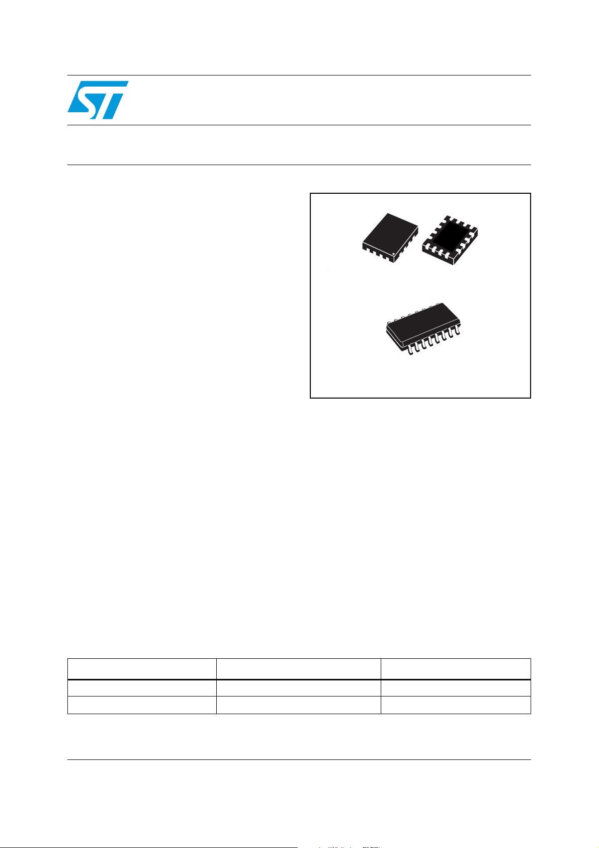
Table 1. Device summary
SO-16
Description
The STMPE801 is a GPIO (General Purpose
Input / Output) port expander able to interface a
main digital ASIC via the two-line bidirectional bus
2
(I
C); separate GPIO Expander IC is often used in
Mobile-Multimedia platforms to solve the
problems of the limited amounts of GPIOs usually
available on the Digital Engine.
The STMPE801 offers great flexibility as each
I/Os is configurable as input, output. This device
has been designed very low quiescent current,
and includes wake up feature for each I/O, to
optimize the power consumption of the IC.
Order codes Package Packaging
STMPE801QTR QFN16L (2.6mm x 1.8mm) Tape and reel (3000 per reel)
STMPE801MTR SO-16 Tape and reel (2500 per reel)
July 2007 Rev 4 1/26
www.st.com
26

Contents STMPE801
Contents
1 Block diagram . . . . . . . . . . . . . . . . . . . . . . . . . . . . . . . . . . . . . . . . . . . . . . 4
2 Pin settings . . . . . . . . . . . . . . . . . . . . . . . . . . . . . . . . . . . . . . . . . . . . . . . . 5
2.1 Pin connection . . . . . . . . . . . . . . . . . . . . . . . . . . . . . . . . . . . . . . . . . . . . . . 5
2.2 Pin assignment . . . . . . . . . . . . . . . . . . . . . . . . . . . . . . . . . . . . . . . . . . . . . . 6
3 Maximum rating . . . . . . . . . . . . . . . . . . . . . . . . . . . . . . . . . . . . . . . . . . . . . 7
3.1 Absolute maximum rating . . . . . . . . . . . . . . . . . . . . . . . . . . . . . . . . . . . . . . 7
3.2 Thermal data . . . . . . . . . . . . . . . . . . . . . . . . . . . . . . . . . . . . . . . . . . . . . . . 7
4 Electrical specification . . . . . . . . . . . . . . . . . . . . . . . . . . . . . . . . . . . . . . . 8
4.1 DC electrical characteristics . . . . . . . . . . . . . . . . . . . . . . . . . . . . . . . . . . . . 8
5 I2C module . . . . . . . . . . . . . . . . . . . . . . . . . . . . . . . . . . . . . . . . . . . . . . . . . 9
5.1 I2C address . . . . . . . . . . . . . . . . . . . . . . . . . . . . . . . . . . . . . . . . . . . . . . . . 9
5.2 I2C features . . . . . . . . . . . . . . . . . . . . . . . . . . . . . . . . . . . . . . . . . . . . . . . 10
5.3 Start condition . . . . . . . . . . . . . . . . . . . . . . . . . . . . . . . . . . . . . . . . . . . . . 11
5.4 Stop condition . . . . . . . . . . . . . . . . . . . . . . . . . . . . . . . . . . . . . . . . . . . . . 11
5.5 Acknowledge bit . . . . . . . . . . . . . . . . . . . . . . . . . . . . . . . . . . . . . . . . . . . . 11
5.6 Data input . . . . . . . . . . . . . . . . . . . . . . . . . . . . . . . . . . . . . . . . . . . . . . . . . 11
5.7 Operation modes . . . . . . . . . . . . . . . . . . . . . . . . . . . . . . . . . . . . . . . . . . . 12
5.8 Read operation . . . . . . . . . . . . . . . . . . . . . . . . . . . . . . . . . . . . . . . . . . . . . 13
5.9 Acknowledgement in read operation . . . . . . . . . . . . . . . . . . . . . . . . . . . . 13
5.10 Write operations . . . . . . . . . . . . . . . . . . . . . . . . . . . . . . . . . . . . . . . . . . . . 13
5.11 General call . . . . . . . . . . . . . . . . . . . . . . . . . . . . . . . . . . . . . . . . . . . . . . . 14
6 Turning I2C block OFF and ON . . . . . . . . . . . . . . . . . . . . . . . . . . . . . . . 14
2/26

STMPE801 Contents
7 Register map . . . . . . . . . . . . . . . . . . . . . . . . . . . . . . . . . . . . . . . . . . . . . . 15
7.1 System and identification registers . . . . . . . . . . . . . . . . . . . . . . . . . . . . . . 15
7.2 System control register . . . . . . . . . . . . . . . . . . . . . . . . . . . . . . . . . . . . . . . 15
8 Interrupt, power supply & reset . . . . . . . . . . . . . . . . . . . . . . . . . . . . . . . 16
8.1 Interrupt enable GPIO mask register (IEGPIOR) . . . . . . . . . . . . . . . . . . . 16
8.2 Interrupt status GPIO register (ISGPIOR) . . . . . . . . . . . . . . . . . . . . . . . . 17
8.3 GPIO controller . . . . . . . . . . . . . . . . . . . . . . . . . . . . . . . . . . . . . . . . . . . . . 17
8.4 Power supply . . . . . . . . . . . . . . . . . . . . . . . . . . . . . . . . . . . . . . . . . . . . . . 18
8.5 Reset . . . . . . . . . . . . . . . . . . . . . . . . . . . . . . . . . . . . . . . . . . . . . . . . . . . . 18
9 Package mechanical data . . . . . . . . . . . . . . . . . . . . . . . . . . . . . . . . . . . . 19
10 Revision history . . . . . . . . . . . . . . . . . . . . . . . . . . . . . . . . . . . . . . . . . . . 25
3/26

Block diagram STMPE801
1 Block diagram
Figure 1. Block diagram
4/26

STMPE801 Pin settings
2 Pin settings
2.1 Pin connection
Figure 2. Pin connection
QFN16L
1
1
2
2
3
3
4
4
Top View
Top View
5
5
6
6
7
7
8
8
16
16
15
15
14
14
13
13
12
12
11
11
10
10
9
9
SO-16
5/26
Pin settings STMPE801
2.2 Pin assignment
Table 2. Pin assignment
Pin N°
SO-16 QFN16L
11 1 INT INT output
12 2 Reset Reset Input (Active Low)
13 3 CLOCK
14 4 Address
Name Function
2
C Clock
I
2
C Address
I
15 5 DATA
16 6 VCC
I2C Data
Supply voltage for I
2
C block
1 7 VIO Supply voltage for GPO and GPIO Controller
(Note: V
must be ≥ VCC)
IO
2 8 GND GND
3 9 GPIO_0 GPIO 0
4 10 GPIO_1 GPIO 1
5 11 GPIO_2 GPIO 2
6 12 GPIO_3 GPIO 3
7 13 GPIO_4 GPIO 4
8 14 GPIO_5 GPIO 5
9 15 GPIO_6 GPIO 6
10 16 GPIO_7 GPIO 7
6/26
STMPE801 Maximum rating
3 Maximum rating
Stressing the device above the rating listed in the “Absolute Maximum Ratings” table may
cause permanent damage to the device. These are stress ratings only and operation of the
device at these or any other conditions above those indicated in the Operating sections of
this specification is not implied. Exposure to Absolute Maximum Rating conditions for
extended periods may affect device reliability. Refer also to the STMicroelectronics SURE
Program and other relevant quality documents.
3.1 Absolute maximum rating
Table 3. Absolute maximum rating
Symbol Parameter Value Unit
V
CC
V
IO
VESD (HBM) ESD protection on each GPO pin 2 KV
Supply voltage 4.5 V
GPO supply voltage 4.5 V
3.2 Thermal data
Table 4. Thermal data
Symbol Parameter
Operating ambient temperature -40 +85 °C
Operating storage temperature -65 155 °C/W
T
T
A
STG
Val ue
Unit
Min Typ Max
7/26

Electrical specification STMPE801
4 Electrical specification
4.1 DC electrical characteristics
Table 5. DC electrical characteristics
Symbol Parameter Test conditions
Min Typ Max
V
Core supply voltage 1.65 - 3.6 V
CC
V
IO supplì voltage 1.65 - 3.6 V
IO
Ipd Power down current 1 µA
Icc Max
Icc
Normal
I
CC
Suspend
V
IL
V
IH
V
OL
VOH
Operating current
(No peripheral activity)
Operating current
(No peripheral activity)
Operating current
(No peripheral activity)
Input voltage low state
Input voltage high state
Output voltage low state
Output voltage high
state
2
I
C running at 400KHz
100% traffic density
2
C running at 400KHz
I
1% traffic density
2
C activity
No I
= 1.8-3.3V
V
IO
= 1.8-3.3V 0.70V
V
IO
= 1.8-3.3V, IOL=8mA
V
IO
-0.3V
-0.3V
VIO=1.8-3.3V, IOL=8mA 0.75VIO V
Value
0.2 0.5 mA
10 15 µA
0.5 1 µA
0.30V
IO
IO
VIO+0.3V
0.25V
IO
+0.3V
IO
Unit
V
V
V
V
VOL (I2C)
V
OH
2
(I
C)
Output voltage low state
Output voltage high
state
Vcc=1.8-3.3V, I
Vcc=1.8-3.3V, I
=8mA
OL
=8mA
OL
-0.3V
0.75Vc
c
0.25V
CC
VCC+0.3V
V
V
8/26

STMPE801 I2C module
5 I2C module
STMPE801 is interface to the main processor using an I2C bus.
5.1 I2C address
Addressing scheme of STMPE801 is designed to allow up to 2 devices to be connected to
the same I
Figure 3. Addressing scheme
Table 6. Addresses
2
C bus.
ADDR0 Address Note
0 0x82
1 0x88
For the bus master to communicate to the slave device, the bus master must initiate a Start
condition anf followed by the slave device address. Accompanying the slave device address,
there is a Read/Write
If a match occurs on the slave device address, the corresponding device gives an
acknowledge on the SDA during the 9
the bus by not responding to the transaction.
bit (R/W). The bit is set to 1 for Read and 0 for write operation.
th
bit time. If there is no match, it deselects itself from
9/26

I2C module STMPE801
Figure 4. I2C timing
Table 7. I
2
C address
Symbol Parameter Min Typ Max Unit
f
SCL
t
LOW
t
HIGH
t
F
t
HD:STA
t
SU:STA
t
SU:DAT
t
HD:DAT
t
SU:STO
t
BUF
SCL clock frequency 0 400 kHz
Clock low period 1.3 µs
Clock high period 600 ns
SDA and SCL fall time 300 ns
START condition hold time
(After this period the first clock is generated)
START condition setup time
(Only relevant for a repeated start period)
Data setup time 100 ns
Data hold time 0 µs
STOP condition setup time 600 ns
Time the bust must be free before a new
trasmission can start
5.2 I2C features
600 ns
600 ns
1.3 µs
The features that are supported by the I2C interface are as below:
2
● I
C slave device
● Operates at 1.8V
● Compliant to Philips I
● Supports standard (uo to 100Kbps) and fast (up to 400Kbps) modes
10/26
2
C specification version 2.1

STMPE801 I2C module
5.3 Start condition
A Start condition is identified by a falling edge of SDATA while SCLK is stable at high state.
A Start condition must precede any data/command transfer. The device continuously
monitors for a Start condition and will not respond to any transaction unless one is
encountered.
5.4 Stop condition
A Stop condition is identified by a rising edge of SDATA while SCLK is stable at high state.
A Stop condition terminates communication between the slave device and bus master. A
read command that is followed by NoAck can be followed by a Stop condition to force the
slave device into idle mode. When the slave device is in idle mode, it is ready to receive the
2
next I
C transaction. A Stop condition at the end of a write command stops the write
operation to registers.
5.5 Acknowledge bit
The acknowledge bit is used to indicate a successful byte transfer. The bus transmitter
releases the SDATA after sending eight bits of data. During the ninth bit, the receiver pulls
the SDATA low to acknowledge the receipt of the eight bits of data. The receiver may leave
the SDATA in high state if it would to not acknowledge the receipt of the data.
5.6 Data input
The device samples the data input on SDATA on the rising edge of the SCLK. The SDATA
signal must be stable during the rising edge of SCLK and the SDATA signal must change
only when SCLK is driven low.
11/26

I2C module STMPE801
M
5.7 Operation modes
Table 8. Operation modes
Mode Bytes Programming Sequence
= 0, Register Address to be read
= 1, Data Read, STOP
= 0, Register Address to be written, Data
Read ≥1
Write ≥1
START, Device Address, R/W
RESTART, Device Address, R/W
If no STOP is issued, the Data Read can be continuously preformed. If
the register address falls within the range that allows address autoincrement, then register address auto-increments internally after every
byte of data being read. For register address that falls within a nonincremental address range, the address will be kept static throughout the
entire read operations. Refer to the Memory Map table for the address
ranges that are auto and non-increment.
START, Device Address, R/W
Write, STOP
If no STOP is issued, the Data Write can be continuously performed. If
the register address falls within the range that allows address autoincrement, then register address auto-increments internally after every
byte of data being written in. For register address that falls within a nonincremental address range, the address will be kept static throughout the
entire write operations. Refer to the Memory Map table for the address
ranges that are auto and non-increment.
Figure 5. Read and write modes (random and sequential)
One Byte
Re ad
More than
One Byte
Re ad
One Byte
Write
ore than
One Byte
Write
Dev
Addr
Star t
Dev
Addr
Start
Dev
Addr
Star t
Dev
Addr
Start
Reg
Addr
RnW=0
Ack
Reg
Addr
RnW=0
Ack
Reg
Addr
RnW=0
Ack
Reg
Addr
RnW=0
Ack
Ack
Ack
Ack
Ack
Dev
Addr
reStart
Dev
Addr
reStart
Data to
be
Written
Data to
Write
RnW=1
RnW=1
Ack
Stop
Data to
Write + 1
Ack
Dat a
Rea d
Ack
Dat a
Rea d
Ack
Ack
Master
Slave
NoAck
Ack
Data to
Write + 2
Stop
Dat a
Rea d + 1
Ack
Stop
Dat a
Rea d + 2
Ack
NoAck
Stop
12/26

STMPE801 I2C module
5.8 Read operation
A write is first performed to load the register address into the Address Counter but without
sending a Stop condition. Then, the bus master sends a reStart condition and repeats the
Device Address with the R/W
content of the addressed byte. If no more data is to be read, the bus master must not
acknowledge the byte and terminates the transfer with a Stop condition.
If the bus master acknowledges the data byte, then it can continue to perform the data
reading. To terminate the stream of data byte, the bus master must not acknowledge the
last output byte and follow by a Stop condition. If the address of the register written into the
Address Counter falls within the range of addresses that has the auto-increment function,
the data being read will be coming from consecutive addresses, with the internal Address
Counter automatically increments after each byte output. After the last memory address,
the Address Counter 'rolls-over' and the device continue to output data from the memory
address of 0x00. Similarly, for the address of register that falls within non-increment range
of addresses, the output data byte comes from the same address (which is the address
pointed by the Address Counter).
bit set to 1. The slave device acknowledges and outputs the
5.9 Acknowledgement in read operation
For the above read command, the slave device waits, after each byte read, for an
acknowledgement during the ninth bit time. If the bus master does not drive the SDA to low
state, then the slave device terminates and switches back to its idle mode, waiting for the
next command.
5.10 Write operations
A write is first performed to load the register address into the Address Counter without
sending a Stop condition. After the bus master receives an acknowledgement from the
slave device, it may start to send a data byte to the register (pointed by the Address
Counter). The slave device again acknowledges and the bus master terminates the transfer
with a Stop condition.
If the bus master would like to continue to write more data, it can just continue write
operation without issuing the Stop condition. Whether the Address Counter autoincrements or not after each data byte write, depends on the address of the register written
into the Address Counter. After the bus master writes the last data byte and the slave
device acknowledges the receipt of the last data, the bus master may terminates the write
operation by sending a Stop condition. When the Address Counter reaches the last
memory address, it 'rolls-over' on the next data byte write.
13/26

Turning I2C block OFF and ON STMPE801
5.11 General call
A general call address is a transaction with the slave address of 0x00 and R/W = 0. When a
general call address is made, the device responds to this transaction with an
acknowledgement and behaves as a slave-receiver mode. The meaning of a general call
address is defined in the second byte sent by the master-transmitter.
Table 9. General call
R/W Second Byte Value Definition
0 0x06 2-byte transaction in which the second byte tells the slave device
to reset and write (or latch in) the 1-bit programmable part of the
slave address.
0 0x04 2-byte transaction in which the second byte tells the slave device
not to reset and write (or latch in) the 1-bit programmable part of
the slave address.
0 0x00 Not allowed as second byte.
Note: All other second byte value will be ignored.
6 Turning I2C block OFF and ON
STMPE801 operates entirely on the I2C clock. When there are no activity on the I2C bus,
current consumption of the device is extremely low. However, when there are activity on the
2
I
C bus, current consumption increases, even if the I2C traffic is not directed to the assigned
address.
Host system may choose to shut-down the I
registers are required. This feature allows the current consumption to drop to the minimum.
Host system turns OFF the I
2
C block by writing ‘1’ into the I2C_SHDN bit. The I2C block will
shut down on the next valid clock edge of the I
CANNOT be accessed by I
To turn ON the I
2
I
C block. This could be done by hardware assertion of the RESET pin.
2
C block, system host must reset the STMPE801 in order to re-activate the
2
C, as the I2C has shut down completely.
2
C block in the STMPE801, if no access to the
2
C clock signal. In this state, the device
14/26

STMPE801 Register map
7 Register map
Table 10. Register map
Address Register Name Size (bit) Function
0x00 Chip ID 16 0x0801
0x02 Version ID 8 Revision number
0x04 SystemControl 8 Reset and interrupt control
0x08 IEGPIOR 8 GPIO interrupt enable register
0x09 ISGPIOR 8 GPIO interrupt status register
0x10 GPMR 8 GPIO monitor pin state register
0x11 GPSR 8 GPIO set pin state register
0x12 GPDR 8 GPIO set pin direction register
7.1 System and identification registers
Table 11. System and identification registers
Register name Size (bit) Function
Chip ID 16 0x0801
Version ID 8 Revision number:
0x01 (Engineering)
0x02 (Final silicon)
Systemcontrol 8
7.2 System control register
Table 12. System control register
Bit Reset Name Description
7 0 SoftReset Writing ‘1’ to this bit causes a soft reset
6 0 I2C_SHDN
5 0
4 0
3 0
2 0 INT_Enable ‘1’ to enable, ‘0’ to disable INT output
1 0
0 0 INTPolarity ‘1’ for active HI, ‘0’ for active LOW
Writing ‘1’ to this bit shuts down the I2C block
on the next valid I2C clock.
15/26

Interrupt, power supply & reset STMPE801
8 Interrupt, power supply & reset
STMPE801 could be configured to generate an interrupt when there is a logic transition of
any of the GPIO configured as input.
8.1 Interrupt enable GPIO mask register (IEGPIOR)
IEGPIOR register is used to enable the interruption from a particular GPIO interrupt source
to the host. The IEG[7:0] bits are the interrupt enable mask bits correspond to the GPIO[7:0]
pins.
IEGPIOR
Bit765 432 1 0
IEG7 IEG6 IEG5 IEG4 IEG3 IEG2 IEG1 IEG0
R/WRWRWRWRWRWRW RW RW
Reset
Val u e
000 000 0 0
Table 13. Register
Bits Name Description
7:0 IEG[x]
Interrupt Enable GPIO Mask (where x = 7 to 0)
Writing a ‘1’ to the IE[x] bit will enable the interruption to the host.
16/26

STMPE801 Interrupt, power supply & reset
8.2 Interrupt status GPIO register (ISGPIOR)
ISGPIOR register monitors the status of the interruption from a particular GPIO pin interrupt
source to the host. Regardless whether the IEGPIOR bits are enabled or not, the ISGPIOR
bits are still updated. The ISG[9:0] bits are the interrupt status bits correspond to the
GPIO[7:0] pins.
ISGPIOR
Bit 7 6 5 4 3 2 1 0
ISG7 ISG6 ISG5 ISG4 ISG3 ISG2 ISG1 ISG0
R/W RW RW RW RW RW RW RW RW
Reset
Valu e
00 0 0 0 0 0 0
Table 14. Register
Bits Name Description
7:0 ISG[x]
8.3 GPIO controller
A total of 8 GPIOs are available in the STMPE801 port expander IC. The GPIO controller
contains the registers that allow the host system to configure each of the pins as input or
output. Unused GPIOs should be configured as outputs to minimize the power consumption.
A group of registers are used to control the exact function of each of the 8 GPIO. The
registers and their respective address is listed in the following table.
Interrupt Status GPIO (where x = 7 to 0)
Read:
Interrupt Status of the GPIO[x]. Reading the register will clear any bits that
has been set to ‘1’
Write:
Writing to this register has no effects
Table 15. Register
Address Register Name Description
0x10 GPMR GPIO monitor pin state register Yes
0x11 GPSR GPIO set pin state register Yes
0x12 GPDR GPIO set pin direction register Yes
17/26
(during sequential R/W)
Auto-Increment
Interrupt, power supply & reset STMPE801
All GPIO registers are named as GPxx, where
Xxx represents the functional group
Bit 76543210
GPxx IO-7 IO-6 IO-5 IO-4 IO-3 IO-2 IO-1 IO-0
The function of each bit is shown in the following table:
Table 16. Pin function
Register Name Function
GPIO Monitor Pin State Reading this bit yields the current state of the bit. Writing has no effect.
GPIO Set Pin State Writing ‘1’ to this bit causes the corresponding GPIO to go to ‘1’ state.
Writing ‘0’ to this bit causes the corresponding GPIO to go to ‘0’ state.
GPIO Set Pin Direction ‘0’ sets the corresponding GPIO to input state, and ‘1’ sets it to output
state. All bits are ‘0’ on reset.
On power-up reset, all GPIO are set as input.
8.4 Power supply
STMPE801 GPIO operates from a separate supply pin (VIO). This dedicated supply pin
provides a level-shifting feature to the STMPE801.
GPIO will remain valid until V
The host system may choose to turn off V
However it is not allowed to turn off supply to V
8.5 Reset
STMPE801 is equipped with an internal POR circuit that holds the device in reset state, until
the V
The reset pin allows the host to reset the STMPE801 directly. Minimum pulse width of reset
signal is 100µs.
During the period when reset pin is asserted, all GPIO default to inputs.
supply input is valid. The internal POR is tied to the Vio supply pin.
IO
is removed.
IO
supply while keeping VIO supplied.
CC
, while keeping the Vcc supplied.
IO
18/26

STMPE801 Package mechanical data
9 Package mechanical data
In order to meet environmental requirements, ST offers these devices in ECOPACK®
packages. These packages have a Lead-free second level interconnect . The category of
second level interconnect is marked on the package and on the inner box label, in
compliance with JEDEC Standard JESD97. The maximum ratings related to soldering
conditions are also marked on the inner box label. ECOPACK is an ST trademark.
ECOPACK specifications are available at: www.st.com
19/26

Package mechanical data STMPE801
Table 17. QFN16L mechanical data
mm. inch
Dim.
Min Typ Max Min Typ Max
A 0.45 0.55 0.60 0.020 0.022 0.024
A1 0.02 0.05 0.001 0.002
b 0.15 0.20 0.25 0.006 0.008 0.010
D 2.50 2.60 2.70 0.098 0.102 0.106
E 1.70 1.80 1.90 0.067 0.071 0.075
e 0.40 0.016
L 0.35 0.40 0.45 0.014 0.016 0.018
Figure 6. Package dimensions
20/26

STMPE801 Package mechanical data
Figure 7. Footprint recommendation
Figure 8. Marking
A
B
A: Device Marking (525)
B: Dot
21/26

Package mechanical data STMPE801
Figure 9. QFN16L tape and reel information
22/26

STMPE801 Package mechanical data
Figure 10. QFN16L tape and reel information (continued)
23/26

Package mechanical data STMPE801
Table 18. SO-16 mechanical data
Dim.
Min. Typ Max. Min. Typ. Max.
A 1.75 0.068
a1 0.1 0.25 0.004 0.010
a2 1.64 0.063
b 0.35 0.46 0.013 0.018
b1 0.19 0.25 0.007 0.010
C 0.5 0.019
c1 45° (typ.)
D 9.8 10 0.385 0.393
E 5.8 6.2 0.228 0.244
e 1.27 0.050
e3 8.89 0.350
F 3.8 4.0 0.149 0.157
G 4.6 5.3 0.181 0.208
L 0.5 1.27 0.019 0.050
mm. inch
M 0.62 0.024
S 8° (max.)
Figure 11. Package dimensions
24/26
0016020D

STMPE801 Revision history
10 Revision history
Table 19. Revision history
Date Revision Changes
07-Dec-2006 1 Initial release
22-Jan-2007 2 Added Marking and Reel information
27-Apr-2007 3 Updated Chapter 8.4 and Chapter 8.5 on page 18
02-Jul-2007 4 Coverpage QFN package drawing updated
25/26

STMPE801
Please Read Carefully:
Information in this document is provided solely in connection with ST products. STMicroelectronics NV and its subsidiaries (“ST”) reserve the
right to make changes, corrections, modifications or improvements, to this document, and the products and services described herein at any
time, without notice.
All ST products are sold pursuant to ST’s terms and conditions of sale.
Purchasers are solely responsible for the choice, selection and use of the ST products and services described herein, and ST assumes no
liability whatsoever relating to the choice, selection or use of the ST products and services described herein.
No license, express or implied, by estoppel or otherwise, to any intellectual property rights is granted under this document. If any part of this
document refers to any third party products or services it shall not be deemed a license grant by ST for the use of such third party products
or services, or any intellectual property contained therein or considered as a warranty covering the use in any manner whatsoever of such
third party products or services or any intellectual property contained therein.
UNLESS OTHERWISE SET FORTH IN ST’S TERMS AND CONDITIONS OF SALE ST DISCLAIMS ANY EXPRESS OR IMPLIED
WARRANTY WITH RESPECT TO THE USE AND/OR SALE OF ST PRODUCTS INCLUDING WITHOUT LIMITATION IMPLIED
WARRANTIES OF MERCHANTABILITY, FITNESS FOR A PARTICULAR PURPOSE (AND THEIR EQUIVALENTS UNDER THE LAWS
OF ANY JURISDICTION), OR INFRINGEMENT OF ANY PATENT, COPYRIGHT OR OTHER INTELLECTUAL PROPERTY RIGHT.
UNLESS EXPRESSLY APPROVED IN WRITING BY AN AUTHORIZED ST REPRESENTATIVE, ST PRODUCTS ARE NOT
RECOMMENDED, AUTHORIZED OR WARRANTED FOR USE IN MILITARY, AIR CRAFT, SPACE, LIFE SAVING, OR LIFE SUSTAINING
APPLICATIONS, NOR IN PRODUCTS OR SYSTEMS WHERE FAILURE OR MALFUNCTION MAY RESULT IN PERSONAL INJURY,
DEATH, OR SEVERE PROPERTY OR ENVIRONMENTAL DAMAGE. ST PRODUCTS WHICH ARE NOT SPECIFIED AS "AUTOMOTIVE
GRADE" MAY ONLY BE USED IN AUTOMOTIVE APPLICATIONS AT USER’S OWN RISK.
Resale of ST products with provisions different from the statements and/or technical features set forth in this document shall immediately void
any warranty granted by ST for the ST product or service described herein and shall not create or extend in any manner whatsoever, any
liability of ST.
ST and the ST logo are trademarks or registered trademarks of ST in various countries.
Information in this document supersedes and replaces all information previously supplied.
The ST logo is a registered trademark of STMicroelectronics. All other names are the property of their respective owners.
© 2007 STMicroelectronics - All rights reserved
STMicroelectronics group of companies
Australia - Belgium - Brazil - Canada - China - Czech Republic - Finland - France - Germany - Hong Kong - India - Israel - Italy - Japan -
Malaysia - Malta - Morocco - Singapore - Spain - Sweden - Switzerland - United Kingdom - United States of America
www.st.com
26/26
 Loading...