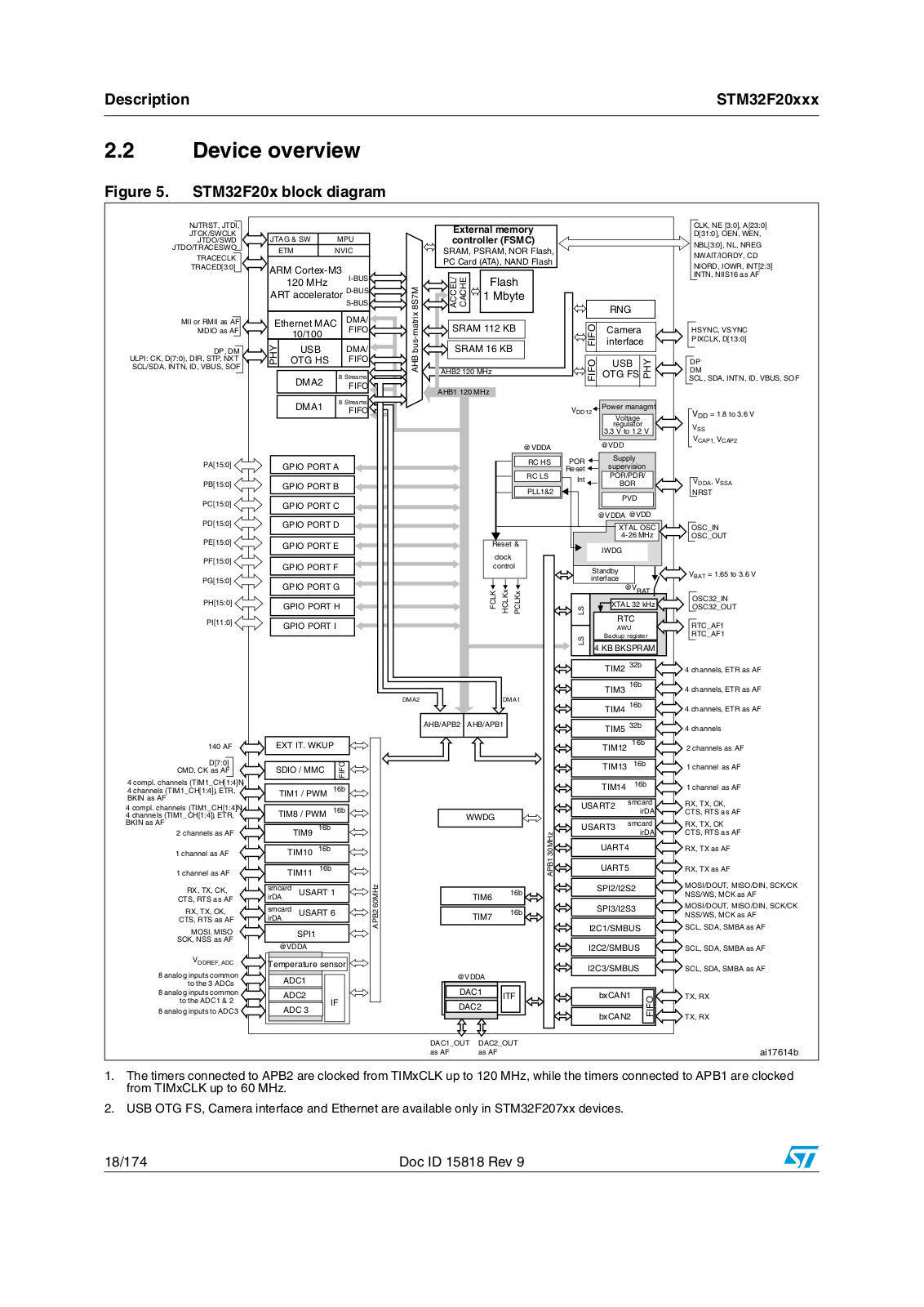
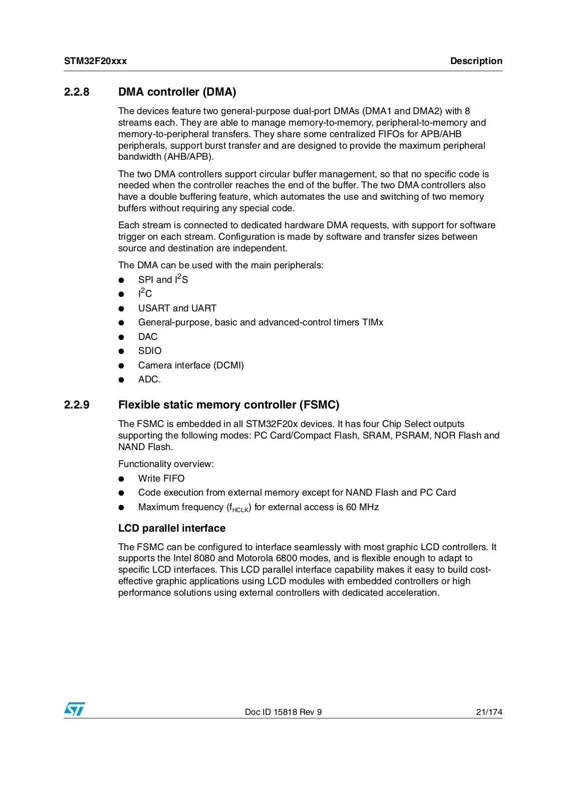
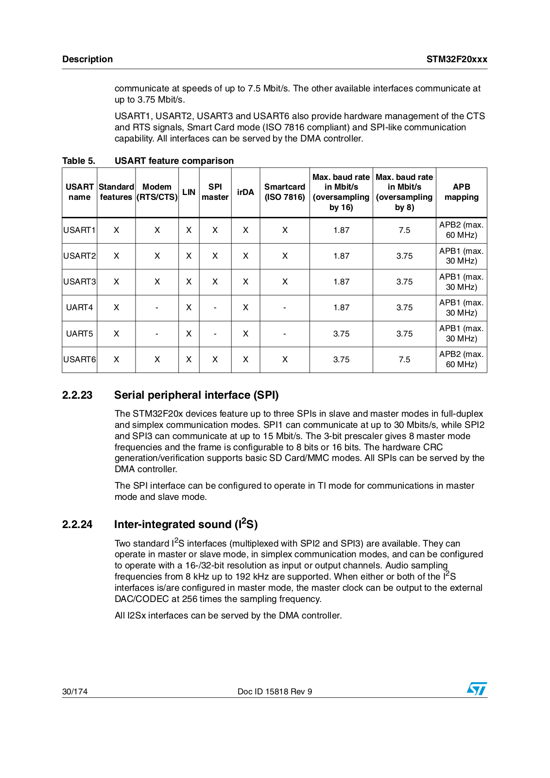
STM32F205xx
STM32F207xx
ARM-based 32-bit MCU, 150DMIPs, up to 1 MB Flash/128+4KB RAM, USB OTG HS/FS, Ethernet, 17 TIMs, 3 ADCs, 15 comm. interfaces & camera
Features
■Core: ARM 32-bit Cortex™-M3 CPU with Adaptive real-time accelerator (ART Accelerator™) allowing 0-wait state execution performance from Flash memory, frequency up to 120 MHz, memory protection unit,
150 DMIPS/1.25 DMIPS/MHz (Dhrystone 2.1)
■Memories
–Up to 1 Mbyte of Flash memory
–512 bytes of OTP memory
–Up to 128 + 4 Kbytes of SRAM
–Flexible static memory controller that supports Compact Flash, SRAM, PSRAM, NOR and NAND memories
–LCD parallel interface, 8080/6800 modes
■Clock, reset and supply management
–From 1.65 to 3.6 V application supply and I/Os
–POR, PDR, PVD and BOR
–4 to 26 MHz crystal oscillator
–Internal 16 MHz factory-trimmed RC (1% accuracy at 25 °C)
–32 kHz oscillator for RTC with calibration
–Internal 32 kHz RC with calibration
■Low power
–Sleep, Stop and Standby modes
–VBAT supply for RTC, 20 × 32 bit backup registers, and optional 4 KB backup SRAM
■3 × 12-bit, 0.5 µs A/D converters
–up to 24 channels
–up to 6 MSPS in triple interleaved mode
■2 × 12-bit D/A converters
■General-purpose DMA
–16-stream DMA controller with centralized FIFOs and burst support
■Up to 17 timers
–Up to twelve 16-bit and two 32-bit timers, up to 120 MHz, each with up to 4 IC/OC/PWM or pulse counter and quadrature (incremental) encoder input
■Debug mode
–Serial wire debug (SWD) & JTAG interfaces
–Cortex-M3 Embedded Trace Macrocell™
|
Datasheet − production data |
||||||||
|
|
|
|
|
|
|
|
||
|
|
FBGA |
|
|
|
|
|
||
|
|
|
|
|
|
|
|||
LQFP64 (10 × 10 mm) |
|
|
|
|
|
FBGA |
|
||
|
|
|
|
|
|
|
|
||
|
|
|
|
|
|
|
|
||
UFBGA176 |
|
|
|
|
|
||||
LQFP100 (14 × 14 mm) |
WLCSP64+2 |
||||||||
LQFP144 (20 × 20 mm) |
(10 × 10 mm) |
||||||||
(0.400 mm pitch) |
|||||||||
LQFP176 (24 × 24 mm) |
|
|
|
||||||
|
|
|
|
|
|
|
|
||
|
|
|
|
|
|
|
|
|
■Up to 140 I/O ports with interrupt capability:
–Up to 136 fast I/Os up to 60 MHz
–Up to 138 5 V-tolerant I/Os
■Up to 15 communication interfaces
–Up to 3 × I2C interfaces (SMBus/PMBus)
–Up to 4 USARTs and 2 UARTs (7.5 Mbit/s, ISO 7816 interface, LIN, IrDA, modem control)
–Up to 3 SPIs (30 Mbit/s), 2 with muxed I2S to achieve audio class accuracy via audio PLL or external PLL
–2 × CAN interfaces (2.0B Active)
–SDIO interface
■Advanced connectivity
–USB 2.0 full-speed device/host/OTG controller with on-chip PHY
–USB 2.0 high-speed/full-speed device/host/OTG controller with dedicated DMA, on-chip full-speed PHY and ULPI
–10/100 Ethernet MAC with dedicated DMA: supports IEEE 1588v2 hardware, MII/RMII
■8- to 14-bit parallel camera interface: up to 48 Mbyte/s
■CRC calculation unit
■96-bit unique ID
■Analog true random number generator
Table 1. |
Device summary |
|
Reference |
Part number |
|
|
|
|
|
STM32F205RB, STM32F205RC, STM32F205RE, |
|
|
STM32F205RF, STM32F205RG, STM32F205VB, |
|
STM32F205xx |
STM32F205VC, STM32F205VE, STM32F205VF |
|
|
STM32F205VG, STM32F205ZC, STM32F205ZE, |
|
|
STM32F205ZF, STM32F205ZG |
|
|
|
|
|
STM32F207IC, STM32F207IE, STM32F207IF, |
|
STM32F207xx |
STM32F207IG, STM32F207ZC, STM32F207ZE, |
|
STM32F207ZF, STM32F207ZG, STM32F207VC, |
||
|
||
|
STM32F207VE, STM32F207VF, STM32F207VG |
|
|
|
April 2012 |
Doc ID 15818 Rev 9 |
1/174 |
This is information on a product in full production. |
www.st.com |
Contents |
STM32F20xxx |
|
|
Contents
1 |
Introduction |
. . . . . . . . . . . . . . . . . . . . . . . . . . . . . . . . . . . . . . . . . . . . . . . |
10 |
|
2 |
Description . . |
. . . . . . . . . . . . . . . . . . . . . . . . . . . . . . . . . . . . . . . . . . . . . . |
11 |
|
|
2.1 |
Full compatibility throughout the family . . . . . . . . . . . . . . . . . . . . . . . . . . |
15 |
|
|
2.2 |
Device overview . . . . . . . . . . . . . . . . . . . . . . . . . . . . . . . . . . . . . . . . . . . . |
18 |
|
|
|
2.2.1 |
ARM® Cortex™-M3 core with embedded Flash and SRAM . . . . . . . . . |
19 |
|
|
2.2.2 |
Adaptive real-time memory accelerator (ART Accelerator™) . . . . . . . . |
19 |
|
|
2.2.3 |
Memory protection unit . . . . . . . . . . . . . . . . . . . . . . . . . . . . . . . . . . . . . |
19 |
|
|
2.2.4 |
Embedded Flash memory . . . . . . . . . . . . . . . . . . . . . . . . . . . . . . . . . . . |
19 |
|
|
2.2.5 |
CRC (cyclic redundancy check) calculation unit . . . . . . . . . . . . . . . . . . |
20 |
|
|
2.2.6 |
Embedded SRAM . . . . . . . . . . . . . . . . . . . . . . . . . . . . . . . . . . . . . . . . . |
20 |
|
|
2.2.7 |
Multi-AHB bus matrix . . . . . . . . . . . . . . . . . . . . . . . . . . . . . . . . . . . . . . . |
20 |
|
|
2.2.8 |
DMA controller (DMA) . . . . . . . . . . . . . . . . . . . . . . . . . . . . . . . . . . . . . . |
21 |
|
|
2.2.9 |
Flexible static memory controller (FSMC) . . . . . . . . . . . . . . . . . . . . . . . |
21 |
|
|
2.2.10 |
Nested vectored interrupt controller (NVIC) . . . . . . . . . . . . . . . . . . . . . . |
22 |
|
|
2.2.11 |
External interrupt/event controller (EXTI) . . . . . . . . . . . . . . . . . . . . . . . |
22 |
|
|
2.2.12 |
Clocks and startup . . . . . . . . . . . . . . . . . . . . . . . . . . . . . . . . . . . . . . . . . |
22 |
|
|
2.2.13 |
Boot modes . . . . . . . . . . . . . . . . . . . . . . . . . . . . . . . . . . . . . . . . . . . . . . |
23 |
|
|
2.2.14 |
Power supply schemes . . . . . . . . . . . . . . . . . . . . . . . . . . . . . . . . . . . . . |
23 |
|
|
2.2.15 |
Power supply supervisor . . . . . . . . . . . . . . . . . . . . . . . . . . . . . . . . . . . . |
23 |
|
|
2.2.16 |
Voltage regulator . . . . . . . . . . . . . . . . . . . . . . . . . . . . . . . . . . . . . . . . . . |
23 |
|
|
2.2.17 |
Real-time clock (RTC), backup SRAM and backup registers . . . . . . . . |
25 |
|
|
2.2.18 |
Low-power modes . . . . . . . . . . . . . . . . . . . . . . . . . . . . . . . . . . . . . . . . . |
26 |
|
|
2.2.19 |
VBAT operation . . . . . . . . . . . . . . . . . . . . . . . . . . . . . . . . . . . . . . . . . . . . |
27 |
|
|
2.2.20 |
Timers and watchdogs . . . . . . . . . . . . . . . . . . . . . . . . . . . . . . . . . . . . . . |
27 |
|
|
2.2.21 |
Inter-integrated circuit interface (I²C) . . . . . . . . . . . . . . . . . . . . . . . . . . . |
29 |
|
|
2.2.22 |
Universal synchronous/asynchronous receiver transmitters |
|
|
|
|
(UARTs/USARTs) . . . . . . . . . . . . . . . . . . . . . . . . . . . . . . . . . . . . . . . . . |
29 |
|
|
2.2.23 |
Serial peripheral interface (SPI) . . . . . . . . . . . . . . . . . . . . . . . . . . . . . . . |
30 |
|
|
2.2.24 |
Inter-integrated sound (I2S) . . . . . . . . . . . . . . . . . . . . . . . . . . . . . . . . . . |
30 |
|
|
2.2.25 |
SDIO . . . . . . . . . . . . . . . . . . . . . . . . . . . . . . . . . . . . . . . . . . . . . . . . . . . |
32 |
2.2.26Ethernet MAC interface with dedicated DMA and IEEE 1588 support . 32
2.2.27 |
Controller area network (CAN) . . . . . . . . . . . . . . . . . . . . . . . . . . . . . . . |
33 |
2.2.28 |
Universal serial bus on-the-go full-speed (OTG_FS) . . . . . . . . . . . . . . . |
33 |
2/175 |
Doc ID 15818 Rev 9 |
STM32F20xxx |
Contents |
|
|
2.2.29 Universal serial bus on-the-go high-speed (OTG_HS) . . . . . . . . . . . . . 33 2.2.30 Audio PLL (PLLI2S) . . . . . . . . . . . . . . . . . . . . . . . . . . . . . . . . . . . . . . . . 34 2.2.31 Digital camera interface (DCMI) . . . . . . . . . . . . . . . . . . . . . . . . . . . . . . . 34 2.2.32 True random number generator (RNG) . . . . . . . . . . . . . . . . . . . . . . . . . 34 2.2.33 GPIOs (general-purpose inputs/outputs) . . . . . . . . . . . . . . . . . . . . . . . . 35 2.2.34 ADCs (analog-to-digital converters) . . . . . . . . . . . . . . . . . . . . . . . . . . . . 35 2.2.35 DAC (digital-to-analog converter) . . . . . . . . . . . . . . . . . . . . . . . . . . . . . . 35 2.2.36 Temperature sensor . . . . . . . . . . . . . . . . . . . . . . . . . . . . . . . . . . . . . . . . 36 2.2.37 Serial wire JTAG debug port (SWJ-DP) . . . . . . . . . . . . . . . . . . . . . . . . . 36 2.2.38 Embedded Trace Macrocell™ . . . . . . . . . . . . . . . . . . . . . . . . . . . . . . . . 36
3 |
Pinouts and pin description . . . . . . . . . . . . . . . . . . . . . . . . . . . . . . . . . . |
37 |
4 |
Memory mapping . . . . . . . . . . . . . . . . . . . . . . . . . . . . . . . . . . . . . . . . . . |
60 |
5 |
Electrical characteristics . . . . . . . . . . . . . . . . . . . . . . . . . . . . . . . . . . . . |
62 |
|
5.1 Parameter conditions . . . . . . . . . . . . . . . . . . . . . . . . . . . . . . . . . . . . . . . . |
62 |
5.1.1 Minimum and maximum values . . . . . . . . . . . . . . . . . . . . . . . . . . . . . . . 62 5.1.2 Typical values . . . . . . . . . . . . . . . . . . . . . . . . . . . . . . . . . . . . . . . . . . . . . 62 5.1.3 Typical curves . . . . . . . . . . . . . . . . . . . . . . . . . . . . . . . . . . . . . . . . . . . . 62 5.1.4 Loading capacitor . . . . . . . . . . . . . . . . . . . . . . . . . . . . . . . . . . . . . . . . . 62 5.1.5 Pin input voltage . . . . . . . . . . . . . . . . . . . . . . . . . . . . . . . . . . . . . . . . . . 62 5.1.6 Power supply scheme . . . . . . . . . . . . . . . . . . . . . . . . . . . . . . . . . . . . . . 63 5.1.7 Current consumption measurement . . . . . . . . . . . . . . . . . . . . . . . . . . . 64
5.2 |
Absolute maximum ratings . . . . . . . . . . . . . . . . . . . . . . . . . . . . . . . . . . . . |
64 |
|
5.3 |
Operating conditions . . . . . . . . . . . . . . . . . . . . . . . . . . . . . . . . . . . . . . . . |
65 |
|
|
5.3.1 |
General operating conditions . . . . . . . . . . . . . . . . . . . . . . . . . . . . . . . . . |
65 |
|
5.3.2 |
VCAP1/VCAP2 external capacitor . . . . . . . . . . . . . . . . . . . . . . . . . . . . . |
68 |
|
5.3.3 |
Operating conditions at power-up / power-down (regulator ON) . . . . . . |
69 |
5.3.4Operating conditions at power-up / power-down (regulator OFF) . . . . . 69
5.3.5 Embedded reset and power control block characteristics . . . . . . . . . . . 70 5.3.6 Supply current characteristics . . . . . . . . . . . . . . . . . . . . . . . . . . . . . . . . 71 5.3.7 Wakeup time from low-power mode . . . . . . . . . . . . . . . . . . . . . . . . . . . . 82 5.3.8 External clock source characteristics . . . . . . . . . . . . . . . . . . . . . . . . . . . 83 5.3.9 Internal clock source characteristics . . . . . . . . . . . . . . . . . . . . . . . . . . . 87 5.3.10 PLL characteristics . . . . . . . . . . . . . . . . . . . . . . . . . . . . . . . . . . . . . . . . 88 5.3.11 PLL spread spectrum clock generation (SSCG) characteristics . . . . . . 91
Doc ID 15818 Rev 9 |
3/175 |
Contents |
STM32F20xxx |
|
|
5.3.12 Memory characteristics . . . . . . . . . . . . . . . . . . . . . . . . . . . . . . . . . . . . . 92 5.3.13 EMC characteristics . . . . . . . . . . . . . . . . . . . . . . . . . . . . . . . . . . . . . . . . 94 5.3.14 Absolute maximum ratings (electrical sensitivity) . . . . . . . . . . . . . . . . . 96 5.3.15 I/O current injection characteristics . . . . . . . . . . . . . . . . . . . . . . . . . . . . 97 5.3.16 I/O port characteristics . . . . . . . . . . . . . . . . . . . . . . . . . . . . . . . . . . . . . . 98 5.3.17 NRST pin characteristics . . . . . . . . . . . . . . . . . . . . . . . . . . . . . . . . . . . 102 5.3.18 TIM timer characteristics . . . . . . . . . . . . . . . . . . . . . . . . . . . . . . . . . . . 103 5.3.19 Communications interfaces . . . . . . . . . . . . . . . . . . . . . . . . . . . . . . . . . 104 5.3.20 12-bit ADC characteristics . . . . . . . . . . . . . . . . . . . . . . . . . . . . . . . . . . 117 5.3.21 DAC electrical characteristics . . . . . . . . . . . . . . . . . . . . . . . . . . . . . . . 122 5.3.22 Temperature sensor characteristics . . . . . . . . . . . . . . . . . . . . . . . . . . . 124 5.3.23 VBAT monitoring characteristics . . . . . . . . . . . . . . . . . . . . . . . . . . . . . . 124 5.3.24 Embedded reference voltage . . . . . . . . . . . . . . . . . . . . . . . . . . . . . . . . 125 5.3.25 FSMC characteristics . . . . . . . . . . . . . . . . . . . . . . . . . . . . . . . . . . . . . . 125 5.3.26 Camera interface (DCMI) timing specifications . . . . . . . . . . . . . . . . . . 143 5.3.27 SD/SDIO MMC card host interface (SDIO) characteristics . . . . . . . . . 143 5.3.28 RTC characteristics . . . . . . . . . . . . . . . . . . . . . . . . . . . . . . . . . . . . . . . 144
6 |
Package characteristics . . . . . . . . . . . . . . . . . . . . . . . . . . . . . . . . . . . . |
145 |
|
|
6.1 |
Package mechanical data . . . . . . . . . . . . . . . . . . . . . . . . . . . . . . . . . . . |
145 |
|
6.2 |
Thermal characteristics . . . . . . . . . . . . . . . . . . . . . . . . . . . . . . . . . . . . . |
152 |
7 |
Part numbering . . . . . . . . . . . . . . . . . . . . . . . . . . . . . . . . . . . . . . . . . . . |
153 |
|
Appendix A Application block diagrams . . . . . . . . . . . . . . . . . . . . . . . . . . . . . . |
154 |
||
|
A.1 |
Main applications versus package . . . . . . . . . . . . . . . . . . . . . . . . . . . . . |
154 |
|
A.2 |
Application example with regulator OFF . . . . . . . . . . . . . . . . . . . . . . . . . |
155 |
|
A.3 |
USB OTG full speed (FS) interface solutions . . . . . . . . . . . . . . . . . . . . . |
156 |
|
A.4 |
USB OTG high speed (HS) interface solutions . . . . . . . . . . . . . . . . . . . . |
158 |
|
A.5 |
Complete audio player solutions . . . . . . . . . . . . . . . . . . . . . . . . . . . . . . . |
159 |
|
A.6 |
Ethernet interface solutions. . . . . . . . . . . . . . . . . . . . . . . . . . . . . . . . . . . |
162 |
8 |
Revision history . . . . . . . . . . . . . . . . . . . . . . . . . . . . . . . . . . . . . . . . . . |
164 |
4/175 |
Doc ID 15818 Rev 9 |
STM32F20xxx |
List of tables |
|
|
List of tables
Table 1. Device summary . . . . . . . . . . . . . . . . . . . . . . . . . . . . . . . . . . . . . . . . . . . . . . . . . . . . . . . . . . 1 Table 2. STM32F205xx features and peripheral counts . . . . . . . . . . . . . . . . . . . . . . . . . . . . . . . . . . 12 Table 3. STM32F207xx features and peripheral counts . . . . . . . . . . . . . . . . . . . . . . . . . . . . . . . . . . 13 Table 4. Timer feature comparison . . . . . . . . . . . . . . . . . . . . . . . . . . . . . . . . . . . . . . . . . . . . . . . . . . 27 Table 5. USART feature comparison . . . . . . . . . . . . . . . . . . . . . . . . . . . . . . . . . . . . . . . . . . . . . . . . 30 Table 6. STM32F20x pin and ball definitions . . . . . . . . . . . . . . . . . . . . . . . . . . . . . . . . . . . . . . . . . . 41 Table 7. FSMC pin definition . . . . . . . . . . . . . . . . . . . . . . . . . . . . . . . . . . . . . . . . . . . . . . . . . . . . . . 52 Table 8. Alternate function mapping . . . . . . . . . . . . . . . . . . . . . . . . . . . . . . . . . . . . . . . . . . . . . . . . . 55 Table 9. Voltage characteristics . . . . . . . . . . . . . . . . . . . . . . . . . . . . . . . . . . . . . . . . . . . . . . . . . . . . 64 Table 10. Current characteristics . . . . . . . . . . . . . . . . . . . . . . . . . . . . . . . . . . . . . . . . . . . . . . . . . . . . 65 Table 11. Thermal characteristics. . . . . . . . . . . . . . . . . . . . . . . . . . . . . . . . . . . . . . . . . . . . . . . . . . . . 65 Table 12. General operating conditions . . . . . . . . . . . . . . . . . . . . . . . . . . . . . . . . . . . . . . . . . . . . . . . 65 Table 13. Limitations depending on the operating power supply range . . . . . . . . . . . . . . . . . . . . . . . 66 Table 14. VCAP1/VCAP2 operating conditions . . . . . . . . . . . . . . . . . . . . . . . . . . . . . . . . . . . . . . . . . 68 Table 15. Operating conditions at power-up / power-down (regulator ON) . . . . . . . . . . . . . . . . . . . . 69 Table 16. Operating conditions at power-up / power-down (regulator OFF). . . . . . . . . . . . . . . . . . . . 69 Table 17. Embedded reset and power control block characteristics. . . . . . . . . . . . . . . . . . . . . . . . . . 70 Table 18. Typical and maximum current consumption in Run mode, code with data processing
running from Flash memory (ART accelerator disabled) . . . . . . . . . . . . . . . . . . . . . . . . . . 72 Table 19. Typical and maximum current consumption in Run mode, code with data processing
running from Flash memory (ART accelerator enabled) or RAM . . . . . . . . . . . . . . . . . . . 73 Table 20. Typical and maximum current consumption in Sleep mode . . . . . . . . . . . . . . . . . . . . . . . . 76 Table 21. Typical and maximum current consumptions in Stop mode . . . . . . . . . . . . . . . . . . . . . . . . 78 Table 22. Typical and maximum current consumptions in Standby mode . . . . . . . . . . . . . . . . . . . . . 79
Table 23. Typical and maximum current consumptions in VBAT mode. . . . . . . . . . . . . . . . . . . . . . . . 79 Table 24. Peripheral current consumption . . . . . . . . . . . . . . . . . . . . . . . . . . . . . . . . . . . . . . . . . . . . . 80
Table 25. Low-power mode wakeup timings . . . . . . . . . . . . . . . . . . . . . . . . . . . . . . . . . . . . . . . . . . . 82 Table 26. High-speed external user clock characteristics. . . . . . . . . . . . . . . . . . . . . . . . . . . . . . . . . . 83 Table 27. Low-speed external user clock characteristics . . . . . . . . . . . . . . . . . . . . . . . . . . . . . . . . . . 83 Table 28. HSE 4-26 MHz oscillator characteristics . . . . . . . . . . . . . . . . . . . . . . . . . . . . . . . . . . . . . . 85
Table 29. LSE oscillator characteristics (fLSE = 32.768 kHz) . . . . . . . . . . . . . . . . . . . . . . . . . . . . . . . 86 Table 30. HSI oscillator characteristics . . . . . . . . . . . . . . . . . . . . . . . . . . . . . . . . . . . . . . . . . . . . . . . 87
Table 31. LSI oscillator characteristics . . . . . . . . . . . . . . . . . . . . . . . . . . . . . . . . . . . . . . . . . . . . . . . 88 Table 32. Main PLL characteristics. . . . . . . . . . . . . . . . . . . . . . . . . . . . . . . . . . . . . . . . . . . . . . . . . . . 88 Table 33. PLLI2S (audio PLL) characteristics . . . . . . . . . . . . . . . . . . . . . . . . . . . . . . . . . . . . . . . . . . 89 Table 34. SSCG parameters constraint . . . . . . . . . . . . . . . . . . . . . . . . . . . . . . . . . . . . . . . . . . . . . . . 91 Table 35. Flash memory characteristics . . . . . . . . . . . . . . . . . . . . . . . . . . . . . . . . . . . . . . . . . . . . . . . 92 Table 36. Flash memory programming . . . . . . . . . . . . . . . . . . . . . . . . . . . . . . . . . . . . . . . . . . . . . . . . 93
Table 37. Flash memory programming with VPP . . . . . . . . . . . . . . . . . . . . . . . . . . . . . . . . . . . . . . . . . . . . . . . . . . . 93
Table 38. Flash memory endurance and data retention . . . . . . . . . . . . . . . . . . . . . . . . . . . . . . . . . . . 94 Table 39. EMS characteristics . . . . . . . . . . . . . . . . . . . . . . . . . . . . . . . . . . . . . . . . . . . . . . . . . . . . . . 95 Table 40. EMI characteristics . . . . . . . . . . . . . . . . . . . . . . . . . . . . . . . . . . . . . . . . . . . . . . . . . . . . . . . 96 Table 41. ESD absolute maximum ratings . . . . . . . . . . . . . . . . . . . . . . . . . . . . . . . . . . . . . . . . . . . . . 96 Table 42. Electrical sensitivities . . . . . . . . . . . . . . . . . . . . . . . . . . . . . . . . . . . . . . . . . . . . . . . . . . . . . 97 Table 43. I/O current injection susceptibility . . . . . . . . . . . . . . . . . . . . . . . . . . . . . . . . . . . . . . . . . . . . 97 Table 44. I/O static characteristics . . . . . . . . . . . . . . . . . . . . . . . . . . . . . . . . . . . . . . . . . . . . . . . . . . . 98 Table 45. Output voltage characteristics . . . . . . . . . . . . . . . . . . . . . . . . . . . . . . . . . . . . . . . . . . . . . . 99 Table 46. I/O AC characteristics . . . . . . . . . . . . . . . . . . . . . . . . . . . . . . . . . . . . . . . . . . . . . . . . . . . . 100
Doc ID 15818 Rev 9 |
5/175 |
List of tables |
STM32F20xxx |
|
|
Table 47. NRST pin characteristics . . . . . . . . . . . . . . . . . . . . . . . . . . . . . . . . . . . . . . . . . . . . . . . . . 102 Table 48. Characteristics of TIMx connected to the APB1 domain . . . . . . . . . . . . . . . . . . . . . . . . . 103
Table 49. Characteristics of TIMx connected to the APB2 domain . . . . . . . . . . . . . . . . . . . . . . . . . 104 Table 50. I2C characteristics. . . . . . . . . . . . . . . . . . . . . . . . . . . . . . . . . . . . . . . . . . . . . . . . . . . . . . . 105
Table 51. SCL frequency (fPCLK1= 30 MHz.,VDD = 3.3 V) . . . . . . . . . . . . . . . . . . . . . . . . . . . . . . . . 106 Table 52. SPI characteristics . . . . . . . . . . . . . . . . . . . . . . . . . . . . . . . . . . . . . . . . . . . . . . . . . . . . . . 107 Table 53. I2S characteristics. . . . . . . . . . . . . . . . . . . . . . . . . . . . . . . . . . . . . . . . . . . . . . . . . . . . . . . 110
Table 54. USB OTG FS startup time . . . . . . . . . . . . . . . . . . . . . . . . . . . . . . . . . . . . . . . . . . . . . . . . 112 Table 55. USB OTG FS DC electrical characteristics. . . . . . . . . . . . . . . . . . . . . . . . . . . . . . . . . . . . 112 Table 56. USB OTG FS electrical characteristics . . . . . . . . . . . . . . . . . . . . . . . . . . . . . . . . . . . . . . . 113 Table 57. USB HS DC electrical characteristics . . . . . . . . . . . . . . . . . . . . . . . . . . . . . . . . . . . . . . . . 113 Table 58. Clock timing parameters . . . . . . . . . . . . . . . . . . . . . . . . . . . . . . . . . . . . . . . . . . . . . . . . . . 113 Table 59. ULPI timing . . . . . . . . . . . . . . . . . . . . . . . . . . . . . . . . . . . . . . . . . . . . . . . . . . . . . . . . . . . . 114 Table 60. Ethernet DC electrical characteristics . . . . . . . . . . . . . . . . . . . . . . . . . . . . . . . . . . . . . . . . 114 Table 61. Dynamics characteristics: Ethernet MAC signals for SMI. . . . . . . . . . . . . . . . . . . . . . . . . 115 Table 62. Dynamics characteristics: Ethernet MAC signals for RMII . . . . . . . . . . . . . . . . . . . . . . . . 115 Table 63. Dynamics characteristics: Ethernet MAC signals for MII . . . . . . . . . . . . . . . . . . . . . . . . . 116 Table 64. ADC characteristics . . . . . . . . . . . . . . . . . . . . . . . . . . . . . . . . . . . . . . . . . . . . . . . . . . . . . 117 Table 65. ADC accuracy . . . . . . . . . . . . . . . . . . . . . . . . . . . . . . . . . . . . . . . . . . . . . . . . . . . . . . . . . 119 Table 66. DAC characteristics . . . . . . . . . . . . . . . . . . . . . . . . . . . . . . . . . . . . . . . . . . . . . . . . . . . . . 122 Table 67. TS characteristics . . . . . . . . . . . . . . . . . . . . . . . . . . . . . . . . . . . . . . . . . . . . . . . . . . . . . . . 124
Table 68. VBAT monitoring characteristics . . . . . . . . . . . . . . . . . . . . . . . . . . . . . . . . . . . . . . . . . . . . 124 Table 69. Embedded internal reference voltage. . . . . . . . . . . . . . . . . . . . . . . . . . . . . . . . . . . . . . . . 125
Table 70. Asynchronous non-multiplexed SRAM/PSRAM/NOR read timings . . . . . . . . . . . . . . . . . 126 Table 71. Asynchronous non-multiplexed SRAM/PSRAM/NOR write timings . . . . . . . . . . . . . . . . . 127 Table 72. Asynchronous multiplexed PSRAM/NOR read timings. . . . . . . . . . . . . . . . . . . . . . . . . . . 128 Table 73. Asynchronous multiplexed PSRAM/NOR write timings . . . . . . . . . . . . . . . . . . . . . . . . . . 129 Table 74. Synchronous multiplexed NOR/PSRAM read timings . . . . . . . . . . . . . . . . . . . . . . . . . . . 131 Table 75. Synchronous multiplexed PSRAM write timings . . . . . . . . . . . . . . . . . . . . . . . . . . . . . . . . 132 Table 76. Synchronous non-multiplexed NOR/PSRAM read timings . . . . . . . . . . . . . . . . . . . . . . . . 133 Table 77. Synchronous non-multiplexed PSRAM write timings . . . . . . . . . . . . . . . . . . . . . . . . . . . . 134 Table 78. Switching characteristics for PC Card/CF read and write cycles in
attribute/common space . . . . . . . . . . . . . . . . . . . . . . . . . . . . . . . . . . . . . . . . . . . . . . . . . . 139 Table 79. Switching characteristics for PC Card/CF read and write cycles in I/O space . . . . . . . . . 140 Table 80. Switching characteristics for NAND Flash read cycles . . . . . . . . . . . . . . . . . . . . . . . . . . . 142 Table 81. Switching characteristics for NAND Flash write cycles. . . . . . . . . . . . . . . . . . . . . . . . . . . 143 Table 82. DCMI characteristics. . . . . . . . . . . . . . . . . . . . . . . . . . . . . . . . . . . . . . . . . . . . . . . . . . . . . 143 Table 83. SD / MMC characteristics . . . . . . . . . . . . . . . . . . . . . . . . . . . . . . . . . . . . . . . . . . . . . . . . . 144 Table 84. RTC characteristics . . . . . . . . . . . . . . . . . . . . . . . . . . . . . . . . . . . . . . . . . . . . . . . . . . . . . 144 Table 85. LQFP64 – 10 x 10 mm 64 pin low-profile quad flat package mechanical data . . . . . . . . . 146 Table 86. WLCSP64+2 - 0.400 mm pitch wafer level chip size package mechanical data . . . . . . . 147 Table 87. LQPF100 – 14 x 14 mm 100-pin low-profile quad flat package mechanical data. . . . . . . 148 Table 88. LQFP144 20 x 20 mm, 144-pin low-profile quad flat package mechanical data. . . . . . . . 149 Table 89. LQFP176 - Low profile quad flat package 24 × 24 × 1.4 mm package mechanical data . 150 Table 90. UFBGA176+25 - ultra thin fine pitch ball grid array 10 × 10 × 0.6 mm mechanical data . 151 Table 91. Package thermal characteristics . . . . . . . . . . . . . . . . . . . . . . . . . . . . . . . . . . . . . . . . . . . . 152 Table 92. Ordering information scheme . . . . . . . . . . . . . . . . . . . . . . . . . . . . . . . . . . . . . . . . . . . . . . 153 Table 93. Main applications versus package for STM32F2xxx microcontrollers . . . . . . . . . . . . . . . 154 Table 94. Document revision history . . . . . . . . . . . . . . . . . . . . . . . . . . . . . . . . . . . . . . . . . . . . . . . . 164
6/175 |
Doc ID 15818 Rev 9 |
STM32F20xxx |
List of figures |
|
|
List of figures
Figure 1. |
Compatible board design between STM32F10xx and STM32F2xx |
|
|
for LQFP64 package. . . . . . . . . . . . . . . . . . . . . . . . . . . . . . . . . . . . . . . . . . . . . . . . . . . . . . |
15 |
Figure 2. |
Compatible board design between STM32F10xx and STM32F2xx |
|
|
for LQFP100 package. . . . . . . . . . . . . . . . . . . . . . . . . . . . . . . . . . . . . . . . . . . . . . . . . . . . . |
16 |
Figure 3. |
Compatible board design between STM32F10xx and STM32F2xx |
|
|
for LQFP144 package. . . . . . . . . . . . . . . . . . . . . . . . . . . . . . . . . . . . . . . . . . . . . . . . . . . . . |
16 |
Figure 4. |
Compatible board design between STM32F10xx and STM32F2xx |
|
|
for LQFP176 package. . . . . . . . . . . . . . . . . . . . . . . . . . . . . . . . . . . . . . . . . . . . . . . . . . . . . |
17 |
Figure 5. |
STM32F20x block diagram . . . . . . . . . . . . . . . . . . . . . . . . . . . . . . . . . . . . . . . . . . . . . . . . . |
18 |
Figure 6. |
Multi-AHB matrix . . . . . . . . . . . . . . . . . . . . . . . . . . . . . . . . . . . . . . . . . . . . . . . . . . . . . . . . . |
20 |
Figure 7. |
Startup in regulator OFF: slow VDD slope |
|
|
- power-down reset risen after VCAP_1/VCAP_2 stabilization . . . . . . . . . . . . . . . . . . . . . . . . |
25 |
Figure 8. |
Startup in regulator OFF: fast VDD slope |
|
|
- power-down reset risen before VCAP_1/VCAP_2 stabilization . . . . . . . . . . . . . . . . . . . . . . |
25 |
Figure 9. |
STM32F20x LQFP64 pinout . . . . . . . . . . . . . . . . . . . . . . . . . . . . . . . . . . . . . . . . . . . . . . . . |
37 |
Figure 10. |
STM32F20x WLCSP64+2 ballout. . . . . . . . . . . . . . . . . . . . . . . . . . . . . . . . . . . . . . . . . . . . |
37 |
Figure 11. |
STM32F20x LQFP100 pinout . . . . . . . . . . . . . . . . . . . . . . . . . . . . . . . . . . . . . . . . . . . . . . . |
38 |
Figure 12. |
STM32F20x LQFP144 pinout . . . . . . . . . . . . . . . . . . . . . . . . . . . . . . . . . . . . . . . . . . . . . . . |
39 |
Figure 13. |
STM32F20x LQFP176 pinout . . . . . . . . . . . . . . . . . . . . . . . . . . . . . . . . . . . . . . . . . . . . . . . |
40 |
Figure 14. |
STM32F20x UFBGA176 ballout . . . . . . . . . . . . . . . . . . . . . . . . . . . . . . . . . . . . . . . . . . . . . |
41 |
Figure 15. |
Memory map . . . . . . . . . . . . . . . . . . . . . . . . . . . . . . . . . . . . . . . . . . . . . . . . . . . . . . . . . . . . |
61 |
Figure 16. |
Pin loading conditions . . . . . . . . . . . . . . . . . . . . . . . . . . . . . . . . . . . . . . . . . . . . . . . . . . . . . |
62 |
Figure 17. |
Pin input voltage . . . . . . . . . . . . . . . . . . . . . . . . . . . . . . . . . . . . . . . . . . . . . . . . . . . . . . . . . |
62 |
Figure 18. |
Power supply scheme . . . . . . . . . . . . . . . . . . . . . . . . . . . . . . . . . . . . . . . . . . . . . . . . . . . . |
63 |
Figure 19. |
Current consumption measurement scheme . . . . . . . . . . . . . . . . . . . . . . . . . . . . . . . . . . . |
64 |
Figure 20. |
Number of wait states versus fCPU and VDD range. . . . . . . . . . . . . . . . . . . . . . . . . . . . . . . |
68 |
Figure 21. |
External capacitor CEXT . . . . . . . . . . . . . . . . . . . . . . . . . . . . . . . . . . . . . . . . . . . . . . . . . . . |
68 |
Figure 22. |
Typical current consumption vs temperature, Run mode, code with data |
|
|
processing running from RAM, and peripherals ON . . . . . . . . . . . . . . . . . . . . . . . . . . . . . . |
74 |
Figure 23. |
Typical current consumption vs temperature, Run mode, code with data |
|
|
processing running from RAM, and peripherals OFF . . . . . . . . . . . . . . . . . . . . . . . . . . . . . |
74 |
Figure 24. |
Typical current consumption vs temperature, Run mode, code with data |
|
|
processing running from Flash, ART accelerator OFF, peripherals ON . . . . . . . . . . . . . . . |
75 |
Figure 25. |
Typical current consumption vs temperature, Run mode, code with data |
|
|
processing running from Flash, ART accelerator OFF, peripherals OFF . . . . . . . . . . . . . . |
75 |
Figure 26. |
Typical current consumption vs temperature in Sleep mode, |
|
|
peripherals ON . . . . . . . . . . . . . . . . . . . . . . . . . . . . . . . . . . . . . . . . . . . . . . . . . . . . . . . . . . |
77 |
Figure 27. |
Typical current consumption vs temperature in Sleep mode, |
|
|
peripherals OFF . . . . . . . . . . . . . . . . . . . . . . . . . . . . . . . . . . . . . . . . . . . . . . . . . . . . . . . . . |
77 |
Figure 28. |
Typical current consumption vs temperature in Stop mode . . . . . . . . . . . . . . . . . . . . . . . . |
78 |
Figure 29. |
High-speed external clock source AC timing diagram . . . . . . . . . . . . . . . . . . . . . . . . . . . . |
84 |
Figure 30. |
Low-speed external clock source AC timing diagram . . . . . . . . . . . . . . . . . . . . . . . . . . . . . |
84 |
Figure 31. |
Typical application with an 8 MHz crystal . . . . . . . . . . . . . . . . . . . . . . . . . . . . . . . . . . . . . . |
85 |
Figure 32. |
Typical application with a 32.768 kHz crystal . . . . . . . . . . . . . . . . . . . . . . . . . . . . . . . . . . . |
86 |
Figure 33. |
ACCHSI versus temperature . . . . . . . . . . . . . . . . . . . . . . . . . . . . . . . . . . . . . . . . . . . . . . . . |
87 |
Figure 34. |
ACCLSI versus temperature . . . . . . . . . . . . . . . . . . . . . . . . . . . . . . . . . . . . . . . . . . . . . . . . |
88 |
Figure 35. |
PLL output clock waveforms in center spread mode . . . . . . . . . . . . . . . . . . . . . . . . . . . . . |
92 |
Figure 36. |
PLL output clock waveforms in down spread mode . . . . . . . . . . . . . . . . . . . . . . . . . . . . . . |
92 |
Doc ID 15818 Rev 9 |
7/175 |
List of figures |
STM32F20xxx |
||
Figure 37. I/O AC characteristics definition . . . . . . . . . . . . . . . . . . . . . . . . . . . . . . . . . . . |
. . . . . . . . . |
101 |
|
Figure 38. Recommended NRST pin protection . . . . . . . . . . . . . . . . . . . . . . . . . . . . . . . . |
. . . . . . . . |
102 |
|
Figure 39. I2C bus AC waveforms and measurement circuit . . . . . . . . . . . . . . . . . . . . . . . |
. . . . . . . . |
106 |
|
Figure 40. SPI timing diagram - slave mode and CPHA = 0 . . . . . . . . . . . . . . . . . . . . . . . |
. . . . . . . . |
108 |
|
Figure 41. SPI timing diagram - slave mode and CPHA = 1(1) . . . . . . . . . . . . . . . . . . . . . |
. . . . . . . . |
108 |
|
Figure 42. SPI timing diagram - master mode(1) . . . . . . . . . . . . . . . . . . . . . . . . . . . . . . . . |
. . . . . . . . |
109 |
|
Figure 43. I2S slave timing diagram (Philips protocol)(1) . . . . . . . . . . . . . . . . . . . . . . . . . . |
. . . . . . . . |
111 |
|
Figure 44. I2S master timing diagram (Philips protocol)(1) . . . . . . . . . . . . . . . . . . . . . . . . . |
. . . . . . . . |
111 |
|
Figure 45. USB OTG FS timings: definition of data signal rise and fall time . . . . . . . . . . . |
. . . . . . . . |
113 |
|
Figure 46. ULPI timing diagram . . . . . . . . . . . . . . . . . . . . . . . . . . . . . . . . . . . . . . . . . . . . . |
. . . . . . . . |
114 |
|
Figure 47. Ethernet SMI timing diagram . . . . . . . . . . . . . . . . . . . . . . . . . . . . . . . . . . . . . . |
. . . . . . . . |
115 |
|
Figure 48. Ethernet RMII timing diagram . . . . . . . . . . . . . . . . . . . . . . . . . . . . . . . . . . . . . . |
. . . . . . . . |
115 |
|
Figure 49. Ethernet MII timing diagram . . . . . . . . . . . . . . . . . . . . . . . . . . . . . . . . . . . . . . . |
. . . . . . . . |
116 |
|
Figure 50. ADC accuracy characteristics . . . . . . . . . . . . . . . . . . . . . . . . . . . . . . . . . . . . . . |
. . . . . . . . |
119 |
|
Figure 51. Typical connection diagram using the ADC . . . . . . . . . . . . . . . . . . . . . . . . . . . |
. . . . . . . . |
120 |
|
Figure 52. Power supply and reference decoupling (VREF+ not connected to VDDA). . . . . |
. . . . . . . . |
121 |
|
Figure 53. Power supply and reference decoupling (VREF+ connected to VDDA). . . . . . . . |
. . . . . . . . |
121 |
|
Figure 54. 12-bit buffered /non-buffered DAC . . . . . . . . . . . . . . . . . . . . . . . . . . . . . . . . . . |
. . . . . . . . |
124 |
|
Figure 55. Asynchronous non-multiplexed SRAM/PSRAM/NOR read waveforms . . . . . . |
. . . . . . . . |
126 |
|
Figure 56. Asynchronous non-multiplexed SRAM/PSRAM/NOR write waveforms . . . . . . |
. . . . . . . . |
127 |
|
Figure 57. Asynchronous multiplexed PSRAM/NOR read waveforms. . . . . . . . . . . . . . . . |
. . . . . . . . |
128 |
|
Figure 58. Asynchronous multiplexed PSRAM/NOR write waveforms . . . . . . . . . . . . . . . |
. . . . . . . . |
129 |
|
Figure 59. Synchronous multiplexed NOR/PSRAM read timings . . . . . . . . . . . . . . . . . . . |
. . . . . . . . |
130 |
|
Figure 60. Synchronous multiplexed PSRAM write timings . . . . . . . . . . . . . . . . . . . . . . . . |
. . . . . . . . |
132 |
|
Figure 61. Synchronous non-multiplexed NOR/PSRAM read timings . . . . . . . . . . . . . . . . |
. . . . . . . . |
133 |
|
Figure 62. Synchronous non-multiplexed PSRAM write timings . . . . . . . . . . . . . . . . . . . . |
. . . . . . . . |
134 |
|
Figure 63. PC Card/CompactFlash controller waveforms for common memory read access . . . . . . |
135 |
||
Figure 64. PC Card/CompactFlash controller waveforms for common memory write access . . . . . . |
136 |
||
Figure 65. PC Card/CompactFlash controller waveforms for attribute memory read |
|
|
|
|
access. . . . . . . . . . . . . . . . . . . . . . . . . . . . . . . . . . . . . . . . . . . . . . . . . . . . . . . . |
. . . . . . . . |
137 |
Figure 66. PC Card/CompactFlash controller waveforms for attribute memory write |
|
|
|
|
access. . . . . . . . . . . . . . . . . . . . . . . . . . . . . . . . . . . . . . . . . . . . . . . . . . . . . . . . |
. . . . . . . . |
138 |
Figure 67. PC Card/CompactFlash controller waveforms for I/O space read access . . . . |
. . . . . . . . |
138 |
|
Figure 68. PC Card/CompactFlash controller waveforms for I/O space write access . . . . |
. . . . . . . . |
139 |
|
Figure 69. NAND controller waveforms for read access . . . . . . . . . . . . . . . . . . . . . . . . . . |
. . . . . . . . |
141 |
|
Figure 70. NAND controller waveforms for write access . . . . . . . . . . . . . . . . . . . . . . . . . . |
. . . . . . . . |
141 |
|
Figure 71. NAND controller waveforms for common memory read access . . . . . . . . . . . . |
. . . . . . . . |
142 |
|
Figure 72. NAND controller waveforms for common memory write access. . . . . . . . . . . . |
. . . . . . . . |
142 |
|
Figure 73. SDIO high-speed mode . . . . . . . . . . . . . . . . . . . . . . . . . . . . . . . . . . . . . . . . . . |
. . . . . . . . |
143 |
|
Figure 74. SD default mode . . . . . . . . . . . . . . . . . . . . . . . . . . . . . . . . . . . . . . . . . . . . . . . . |
. . . . . . . . |
144 |
|
Figure 75. LQFP64 – 10 x 10 mm 64 pin low-profile quad flat package outline . . . . . . . . |
. . . . . . . . |
146 |
|
Figure 76. |
Recommended footprint(1) . . . . . . . . . . . . . . . . . . . . . . . . . . . . . . . . . . . . . . . . |
. . . . . . . . |
146 |
Figure 77. WLCSP64+2 - 0.400 mm pitch wafer level chip size package outline . . . . . . . |
. . . . . . . . |
147 |
|
Figure 78. LQFP100, 14 x 14 mm 100-pin low-profile quad flat package outline . . . . . . . |
. . . . . . . . |
148 |
|
Figure 79. |
Recommended footprint(1) . . . . . . . . . . . . . . . . . . . . . . . . . . . . . . . . . . . . . . . . |
. . . . . . . . |
148 |
Figure 80. LQFP144, 20 x 20 mm, 144-pin low-profile quad |
|
|
|
|
flat package outline . . . . . . . . . . . . . . . . . . . . . . . . . . . . . . . . . . . . . . . . . . . . . . |
. . . . . . . . |
149 |
Figure 81. |
Recommended footprint(1) . . . . . . . . . . . . . . . . . . . . . . . . . . . . . . . . . . . . . . . . |
. . . . . . . . |
149 |
Figure 82. LQFP176 - Low profile quad flat package 24 × 24 × 1.4 mm, package outline . . . . . . . . |
150 |
||
Figure 83. UFBGA176+25 - ultra thin fine pitch ball grid array 10 × 10 × 0.6 mm, package outline . 151 |
|||
Figure 84. Regulator OFF/internal reset ON . . . . . . . . . . . . . . . . . . . . . . . . . . . . . . . . . . . |
. . . . . . . . |
155 |
|
Figure 85. |
Regulator OFF/ internal reset OFF . . . . . . . . . . . . . . . . . . . . . . . . . . . . . . . . . . |
. . . . . . . . |
155 |
8/175 |
Doc ID 15818 Rev 9 |
STM32F20xxx |
List of figures |
|
|
Figure 86. USB OTG FS (full speed) device-only connection . . . . . . . . . . . . . . . . . . . . . . . . . . . . . . 156 Figure 87. USB OTG FS (full speed) host-only connection . . . . . . . . . . . . . . . . . . . . . . . . . . . . . . . . 156 Figure 88. OTG FS (full speed) connection dual-role with internal PHY . . . . . . . . . . . . . . . . . . . . . . 157 Figure 89. OTG HS (high speed) device connection, host and dual-role
in high-speed mode with external PHY. . . . . . . . . . . . . . . . . . . . . . . . . . . . . . . . . . . . . . . 158 Figure 90. Complete audio player solution 1 . . . . . . . . . . . . . . . . . . . . . . . . . . . . . . . . . . . . . . . . . . . 159 Figure 91. Complete audio player solution 2 . . . . . . . . . . . . . . . . . . . . . . . . . . . . . . . . . . . . . . . . . . . 159 Figure 92. Audio player solution using PLL, PLLI2S, USB and 1 crystal . . . . . . . . . . . . . . . . . . . . . . 160 Figure 93. Audio PLL (PLLI2S) providing accurate I2S clock . . . . . . . . . . . . . . . . . . . . . . . . . . . . . . 160 Figure 94. Master clock (MCK) used to drive the external audio DAC. . . . . . . . . . . . . . . . . . . . . . . . 161 Figure 95. Master clock (MCK) not used to drive the external audio DAC. . . . . . . . . . . . . . . . . . . . . 161 Figure 96. MII mode using a 25 MHz crystal . . . . . . . . . . . . . . . . . . . . . . . . . . . . . . . . . . . . . . . . . . . 162 Figure 97. RMII with a 50 MHz oscillator . . . . . . . . . . . . . . . . . . . . . . . . . . . . . . . . . . . . . . . . . . . . . . 162 Figure 98. RMII with a 25 MHz crystal and PHY with PLL . . . . . . . . . . . . . . . . . . . . . . . . . . . . . . . . . 163
Doc ID 15818 Rev 9 |
9/175 |
Introduction |
STM32F20xxx |
|
|
This datasheet provides the description of the STM32F205xx and STM32F207xx lines of microcontrollers. For more details on the whole STMicroelectronics STM32™ family, please refer to Section 2.1: Full compatibility throughout the family.
The STM32F205xx and STM32F207xx datasheet should be read in conjunction with the STM32F20x/STM32F21x reference manual. They will be referred to as STM32F20x devices throughout the document.
For information on programming, erasing and protection of the internal Flash memory, please refer to the STM32F20x/STM32F21x Flash programming manual (PM0059).
The reference and Flash programming manuals are both available from the
STMicroelectronics website www.st.com.
For information on the Cortex™-M3 core please refer to the Cortex™-M3 Technical Reference Manual, available from the www.arm.com website at the following address: http://infocenter.arm.com/help/index.jsp?topic=/com.arm.doc.ddi0337e/.
10/174 |
Doc ID 15818 Rev 9 |
STM32F20xxx |
Description |
|
|
The STM32F20x family is based on the high-performance ARM® Cortex™-M3 32-bit RISC core operating at a frequency of up to 120 MHz. The family incorporates high-speed embedded memories (Flash memory up to 1 Mbyte, up to 128 Kbytes of system SRAM), up to 4 Kbytes of backup SRAM, and an extensive range of enhanced I/Os and peripherals connected to two APB buses, two AHB buses and a 32-bit multi-AHB bus matrix.
The devices also feature an adaptive real-time memory accelerator (ART Accelerator™) which allows to achieve a performance equivalent to 0 wait state program execution from Flash memory at a CPU frequency up to 120 MHz. This performance has been validated using the CoreMark benchmark.
All devices offer three 12-bit ADCs, two DACs, a low-power RTC, twelve general-purpose 16-bit timers including two PWM timers for motor control, two general-purpose 32-bit timers. a true number random generator (RNG). They also feature standard and advanced communication interfaces. New advanced peripherals include an SDIO, an enhanced flexible static memory control (FSMC) interface (for devices offered in packages of 100 pins and more), and a camera interface for CMOS sensors. The devices also feature standard peripherals.
●Up to three I2Cs
●Three SPIs, two I2Ss. To achieve audio class accuracy, the I2S peripherals can be clocked via a dedicated internal audio PLL or via an external PLL to allow synchronization.
●4 USARTs and 2 UARTs
●A USB OTG full-speed with high-speed capability (with the ULPI)
●A second USB OTG (full-speed)
●Two CANs
●An SDIO interface
●Ethernet and camera interface available on STM32F207xx devices only.
Note: |
The STM32F205xx and STM32F207xx devices operate in the –40 to +105 °C temperature |
|
range from a 1.8 V to 3.6 V power supply. The supply voltage can drop to 1.7 V when the |
|
device operates in the 0 to 70 °C temperature range and IRROFF is connected to VDD. |
|
A comprehensive set of power-saving modes allow the design of low-power applications. |
STM32F205xx and STM32F207xx devices are offered in four packages ranging from 64 pins to 176 pins. The set of included peripherals changes with the device chosen.These features make the STM32F205xx and STM32F207xx microcontroller family suitable for a wide range of applications:
●Motor drive and application control
●Medical equipment
●Industrial applications: PLC, inverters, circuit breakers
●Printers, and scanners
●Alarm systems, video intercom, and HVAC
●Home audio appliances
Figure 5 shows the general block diagram of the device family.
Doc ID 15818 Rev 9 |
11/174 |
12/174
9 Rev 15818 ID Doc
Table 2. |
STM32F205xx features and peripheral counts |
|
|
|
|
|
|
|
|
|
|
|
|
|
|||||
|
Peripherals |
|
STM32F205Rx |
|
|
|
|
STM32F205Vx |
|
STM32F205Zx |
|||||||||
|
|
|
|
|
|
|
|
|
|
|
|
|
|
|
|
|
|
|
|
Flash memory in Kbytes |
128 |
256 |
512 |
|
768 |
1024 |
128 |
|
256 |
|
512 |
768 |
1024 |
256 |
|
512 |
768 |
1024 |
|
|
|
|
|
|
|
|
|
|
|
|
|
|
|
|
|
|
|
|
|
|
System |
64 |
96 |
|
|
128 |
|
64 |
|
96 |
|
|
128 |
|
96 |
|
128 |
|
|
SRAM in Kbytes |
(SRAM1+SRAM2) |
(48+16) |
(80+16) |
(112+16) |
|
(48+16) |
|
(80+16) |
|
|
(112+16) |
(80+16) |
|
(112+16) |
|||||
|
|
|
|
|
|
|
|
|
|
|
|
|
|
|
|
|
|
|
|
|
Backup |
|
|
4 |
|
|
|
|
4 |
|
|
|
|
4 |
|
|
|||
|
|
|
|
|
|
|
|
|
|
|
|
|
|
|
|
|
|
|
|
FSMC memory controller |
|
|
No |
|
|
|
|
|
|
|
|
Yes(1) |
|
|
|
|
|
||
Ethernet |
|
|
|
|
|
|
|
|
|
No |
|
|
|
|
|
|
|
|
|
|
|
|
|
|
|
|
|
|
|
|
|
|
|
|
|
|
|
|
|
|
General-purpose |
|
|
|
|
|
|
|
10 |
|
|
|
|
|
|
|
|
|
|
|
|
|
|
|
|
|
|
|
|
|
|
|
|
|
|
|
|
|
|
Timers |
Advanced-control |
|
|
|
|
|
|
|
2 |
|
|
|
|
|
|
|
|
|
|
|
|
|
|
|
|
|
|
|
|
|
|
|
|
|
|
|
|
|
|
|
Basic |
|
|
|
|
|
|
|
2 |
|
|
|
|
|
|
|
|
|
|
|
|
|
|
|
|
|
|
|
|
|
|
|
|
|
|
|
|
|
|
Random number generator |
|
|
|
|
|
|
|
|
Yes |
|
|
|
|
|
|
|
|
||
|
|
|
|
|
|
|
|
|
|
|
|
|
|
|
|
|
|
|
|
|
SPI/(I2S) |
|
|
|
|
|
|
|
3 (2)(2) |
|
|
|
|
|
|
|
|
|
|
|
I2C |
|
|
|
|
|
|
|
3 |
|
|
|
|
|
|
|
|
|
|
|
USART |
|
|
|
|
|
|
|
4 |
|
|
|
|
|
|
|
|
|
|
Comm. |
UART |
|
|
|
|
|
|
|
2 |
|
|
|
|
|
|
|
|
|
|
interfaces |
|
|
|
|
|
|
|
|
|
|
|
|
|
|
|
|
|
|
|
USB OTG FS |
|
|
|
|
|
|
|
|
Yes |
|
|
|
|
|
|
|
|
||
|
|
|
|
|
|
|
|
|
|
|
|
|
|
|
|
|
|||
|
|
|
|
|
|
|
|
|
|
|
|
|
|
|
|
|
|
|
|
|
USB OTG HS |
|
|
|
|
|
|
|
|
Yes |
|
|
|
|
|
|
|
|
|
|
|
|
|
|
|
|
|
|
|
|
|
|
|
|
|
|
|
|
|
|
CAN |
|
|
|
|
|
|
|
2 |
|
|
|
|
|
|
|
|
|
|
|
|
|
|
|
|
|
|
|
|
|
|
|
|
|
|
|
|
|
|
Camera interface |
|
|
|
|
|
|
|
|
|
No |
|
|
|
|
|
|
|
|
|
|
|
|
|
|
|
|
|
|
|
|
|
|
|
|
|
|
|
|
|
GPIOs |
|
|
|
51 |
|
|
|
|
82 |
|
|
|
|
114 |
|
|
|||
|
|
|
|
|
|
|
|
|
|
|
|
|
|
|
|
|
|
|
|
SDIO |
|
|
|
|
|
|
|
|
|
Yes |
|
|
|
|
|
|
|
|
|
|
|
|
|
|
|
|
|
|
|
|
|
|
|
|
|
|
|
|
|
12-bit ADC |
|
|
|
|
|
|
|
|
3 |
|
|
|
|
|
|
|
|
|
|
|
|
|
|
|
|
|
|
|
|
|
|
|
|
|
|
|
|
|
|
Number of channels |
|
|
16 |
|
|
|
|
16 |
|
|
|
|
24 |
|
|
||||
|
|
|
|
|
|
|
|
|
|
|
|
|
|
||||||
|
|
|
|
|
|
|
|
|
|
|
|
|
|
|
|
|
|
|
|
12-bit DAC |
|
|
|
|
|
|
|
|
|
Yes |
|
|
|
|
|
|
|
|
|
Number of channels |
|
|
|
|
|
|
|
2 |
|
|
|
|
|
|
|
|
|
||
|
|
|
|
|
|
|
|
|
|
|
|
|
|
|
|
|
|||
Maximum CPU frequency |
|
|
|
|
|
|
|
120 MHz |
|
|
|
|
|
|
|
|
|||
|
|
|
|
|
|
|
|
|
|
|
|
|
|
|
|
|
|||
Operating voltage |
|
|
|
|
|
|
|
1.8 V to 3.6 V(3) |
|
|
|
|
|
|
|
|
|||
Operating temperatures |
|
|
|
|
Ambient temperatures: –40 to +85 °C /–40 to +105 °C |
|
|
|
|
|
|||||||||
|
|
|
|
|
|
|
|
|
|
|
|
|
|
|
|
|
|
||
|
|
|
|
|
Junction temperature: –40 to + 125 °C |
|
|
|
|
|
|||||||||
|
|
|
|
|
|
|
|
|
|
|
|
||||||||
|
|
|
|
|
|
|
|
|
|
|
|
|
|
|
|
|
|
|
|
|
|
|
|
LQFP64 |
|
LQFP6 |
LQFP64 |
|
|
|
|
|
|
|
|
|
|
|
|
Package |
|
LQFP64 |
WLCSP64 |
|
WLCSP6 |
|
|
LQFP100 |
|
|
|
|
LQFP144 |
||||||
|
|
|
|
+2 |
|
4 |
4+2 |
|
|
|
|
|
|
|
|
|
|
|
|
|
|
|
|
|
|
|
|
|
|
|
|
|
|
|
|
|
|
||
|
|
|
|
|
|
|
|
|
|
|
|
|
|
|
|
|
|
|
|
Description
STM32F20xxx
1. For the LQFP100 package, only FSMC Bank1 or Bank2 are available. Bank1 can only support a multiplexed NOR/PSRAM memory using the NE1 Chip Select. Bank2 can only support a 16or 8-bit NAND Flash memory using the NCE2 Chip Select. The interrupt line cannot be used since Port G is not available in this package.
2.The SPI2 and SPI3 interfaces give the flexibility to work in an exclusive way in either the SPI mode or the I2S audio mode.
3.VDD minimum value is 1.7 V when the device operates in the 0 to 70 °C temperature range and IRROFF is set to VDD.
|
Table 3. |
STM32F207xx features and peripheral counts |
|
|
|
|
|
|
|
|
|
|
|
|
||||
|
|
|
Peripherals |
|
STM32F207Vx |
|
|
STM32F207Zx |
|
|
STM32F207Ix |
|
||||||
|
|
|
|
|
|
|
|
|
|
|
|
|
|
|
|
|
||
|
Flash memory in Kbytes |
256 |
512 |
768 |
1024 |
256 |
512 |
|
768 |
|
1024 |
256 |
512 |
|
768 |
1024 |
||
|
|
|
|
|
|
|
|
|
|
|
|
|
|
|
|
|
|
|
|
|
|
System |
|
|
|
|
|
|
128 |
|
|
|
|
|
|
||
|
SRAM in Kbytes |
|
(SRAM1+SRAM2) |
|
|
|
|
|
|
(112+16) |
|
|
|
|
|
|||
|
|
|
|
|
|
|
|
|
|
|
|
|
|
|
|
|
|
|
|
|
|
Backup |
|
|
|
|
|
|
4 |
|
|
|
|
|
|
||
|
|
|
|
|
|
|
|
|
|
|
|
|
|
|
|
|
|
|
|
FSMC memory controller |
|
|
|
|
|
|
|
Yes(1) |
|
|
|
|
|
|
|||
|
Ethernet |
|
|
|
|
|
|
|
|
|
Yes |
|
|
|
|
|
|
|
|
|
|
|
|
|
|
|
|
|
|
|
|
|
|
|
|
|
|
Doc |
|
|
General-purpose |
|
|
|
|
|
|
10 |
|
|
|
|
|
|
||
|
|
|
|
|
|
|
|
|
|
|
|
|
|
|
|
|||
Timers |
|
Advanced-control |
|
|
|
|
|
|
2 |
|
|
|
|
|
|
|||
ID |
|
|
|
|
|
|
|
|
|
|
|
|
|
|
|
|
|
|
|
|
Basic |
|
|
|
|
|
|
2 |
|
|
|
|
|
|
|||
15818 |
|
|
|
|
|
|
|
|
|
|
|
|
|
|
||||
|
|
|
|
|
|
|
|
|
|
|
|
|
|
|
|
|
|
|
|
|
SPI/(I2S) |
|
|
|
|
|
|
3 (2)(2) |
|
|
|
|
|
|
|||
|
Random number generator |
|
|
|
|
|
|
|
Yes |
|
|
|
|
|
|
|||
Rev |
|
|
|
|
|
|
|
|
|
|
|
|
|
|
|
|
||
|
|
I2C |
|
|
|
|
|
|
3 |
|
|
|
|
|
|
|||
9 |
|
|
|
|
|
|
|
|
|
|
|
|
|
|
|
|
|
|
|
|
USART |
|
|
|
|
|
|
4 |
|
|
|
|
|
|
|||
|
|
|
|
|
|
|
|
|
|
|
|
|
|
|
||||
|
Comm. interfaces |
|
UART |
|
|
|
|
|
|
2 |
|
|
|
|
|
|
||
|
|
|
|
|
|
|
|
|
|
|
|
|
|
|
|
|
|
|
|
|
|
USB OTG FS |
|
|
|
|
|
|
|
Yes |
|
|
|
|
|
|
|
|
|
|
|
|
|
|
|
|
|
|
|
|
|
|
|
|
|
|
|
|
|
USB OTG HS |
|
|
|
|
|
|
|
Yes |
|
|
|
|
|
|
|
|
|
|
|
|
|
|
|
|
|
|
|
|
|
|
|
|
||
|
|
|
CAN |
|
|
|
|
|
|
2 |
|
|
|
|
|
|
||
|
|
|
|
|
|
|
|
|
|
|
|
|
|
|
|
|
|
|
|
Camera interface |
|
|
|
|
|
|
|
|
|
Yes |
|
|
|
|
|
|
|
|
|
|
|
|
|
|
|
|
|
|
|
|
|
|
|
|
|
|
|
GPIOs |
|
|
|
|
82 |
|
|
|
114 |
|
|
|
|
140 |
|
||
|
|
|
|
|
|
|
|
|
|
|
|
|
|
|
|
|
|
|
|
SDIO |
|
|
|
|
|
|
|
|
|
Yes |
|
|
|
|
|
|
|
|
|
|
|
|
|
|
|
|
|
|
|
|
|
|
|
|
||
|
12-bit ADC |
|
|
|
|
|
|
|
|
3 |
|
|
|
|
|
|
||
|
|
|
|
|
|
|
|
|
|
|
|
|
|
|
|
|
|
|
|
Number of channels |
|
|
16 |
|
|
|
24 |
|
|
|
|
24 |
|
||||
|
|
|
|
|
|
|
|
|
|
|
|
|
|
|||||
|
|
|
|
|
|
|
|
|
|
|
|
|
|
|
|
|
|
|
|
12-bit DAC |
|
|
|
|
|
|
|
|
|
Yes |
|
|
|
|
|
|
|
|
Number of channels |
|
|
|
|
|
|
2 |
|
|
|
|
|
|
||||
|
|
|
|
|
|
|
|
|
|
|
|
|
|
|
||||
13/174 |
Maximum CPU frequency |
|
|
|
|
|
|
|
120 MHz |
|
|
|
|
|
||||
|
|
|
|
|
|
|
|
|
|
|
|
|
|
|
|
|
|
|
Operating voltage |
|
|
|
|
|
|
|
|
|
1.8 V to 3.6 V(3) |
|
|
|
|
|
|||
|
|
|
|
|
|
|
|
|
|
|
|
|
|
|
STM32F20xxx
Description
14/174 |
Table 3. |
STM32F207xx features and peripheral counts (continued) |
|
|||
|
Peripherals |
STM32F207Vx |
STM32F207Zx |
|
STM32F207Ix |
|
|
|
|
||||
|
|
|
|
|
|
|
|
Operating temperatures |
|
Ambient temperatures: –40 to +85 °C/–40 to +105 °C |
|
||
|
|
|
|
|
||
|
|
Junction temperature: –40 to + 125 °C |
|
|||
|
|
|
|
|
||
|
|
|
|
|
|
|
|
Package |
|
LQFP100 |
LQFP144 |
|
LQFP176/ |
|
|
|
UFBGA176 |
|||
|
|
|
|
|
|
|
|
|
|
|
|
|
|
1.For the LQFP100 package, only FSMC Bank1 or Bank2 are available. Bank1 can only support a multiplexed NOR/PSRAM memory using the NE1 Chip Select. Bank2 can only support a 16or 8-bit NAND Flash memory using the NCE2 Chip Select. The interrupt line cannot be used since Port G is not available in this package.
2.The SPI2 and SPI3 interfaces give the flexibility to work in an exclusive way in either the SPI mode or the I2S audio mode.
3.VDD minimum value is 1.7 V when the device operates in the 0 to 70 °C temperature range and IRROFF is set to VDD.
9 Rev 15818 ID Doc
Description
STM32F20xxx
STM32F20xxx |
Description |
|
|
The STM32F205xx and STM32F207xx constitute the STM32F20x family whose members are fully pin-to-pin, software and feature compatible, allowing the user to try different memory densities and peripherals for a greater degree of freedom during the development cycle.
The STM32F205xx and STM32F207xx devices maintain a close compatibility with the whole STM32F10xxx family. All functional pins are pin-to-pin compatible. The STM32F205xx and STM32F207xx, however, are not drop-in replacements for the STM32F10xxx devices: the two families do not have the same power scheme, and so their power pins are different. Nonetheless, transition from the STM32F10xxx to the STM32F20x family remains simple as only a few pins are impacted.
Figure 3, Figure 4, and Figure 1 provide compatible board designs between the STM32F20x and the STM32F10xxx family.
|
|
|
|
|
|
|
|
|
|
|
|
|
|
|
|
|
|
|
|
|
|
|
|
|
|
|
|
|
|
|
|
|
|
|
|
|
|
|
|
|
|
|
|
|
|
|
|
|
|
|
|
|
|
|
|
|
|
|
|
|
|
|
|
|
|
|
|
|
|
|
|
|
|
|
|
|
|
|
|
|
|
|
|
|
|
|
|
|
|
|
|
|
|
|
|
|
|
|
|
|
|
|
|
|
VSS |
||
|
48 |
|
VSS |
33 |
|
|
|
|
|
|
|
|
|
|
|
|
|
|
|
|
|
|
|
|||
49 |
47 |
|
|
|
|
|
32 |
|
|
|
|
|
|
|
|
|
|
|
|
|
|
|
|
|
|
|
|
|
|
|
|
|
|
31 |
|
|
|
|
|
|
|
|
|
|
|
|
|
|
|
|
|
|
|
|
|
|
|
|
|
|
|
|
|
|
|
|
|
|
|
|
|
|
|
|
|
|
|
|
|
|
|
|
|
|
|
|
|
|
|
|
|
|
|
|
|
|
|
|
|
|
|
|
|
|
|
|
|
|
|
|
|
|
|
|
|
|
|
|
|
|
|
|
|
|
|
|
|
|
|
|
|
|
|
|
|
|
|
|
|
|
|
|
|
|
|
|
|
|
|
|
|
|
VSS |
||||||||
|
|
|
|
|
|
|
|
|
VSS |
|
|
|
|
|
|
|
|
|
|
|
|
|
||||
|
|
|
|
|
|
|
|
0 Ω resistor or soldering bridge |
||||||||||||||||||
|
|
|
|
|
|
|
|
|
|
|
|
|
|
present for the STM32F10xx |
||||||||||||
|
|
|
|
|
|
|
|
|
|
|
|
|
|
configuration, not present in the |
||||||||||||
|
|
|
|
|
|
|
|
|
|
|
|
|
|
STM32F2xx configuration |
||||||||||||
64 |
|
|
|
|
|
|
|
17 |
|
|
|
|
|
|
|
|
|
|
|
|
|
|
|
|
|
|
|
|
|
|
|
|
|
|
|
|
|
|
|
|
|
|
|
|
|
|
|
|
|
|
|
|
|
|
1 |
|
|
|
|
|
16 |
|
|
|
|
|
|
|
|
|
|
|
|
|
|
|
|
|
|
|
ai15962b
Doc ID 15818 Rev 9 |
15/174 |
Description |
STM32F20xxx |
|
|
|
|
|
|
|
|
|
|
|
|
|
|
|
|
|
|
|
|
|
|
|
|
|
|
|
|
|
|
|
|
|
|
|
|
|
|
|
|
|
|
|
|
|
|
|
|
|
|
|
|
|
|
|
|
|
|
|
|
|
|
|
|
|
|
|
|
|
|
|
|
|
|
|
|
|
|
|
|
|
|
|
633 |
|
|
|
|
|
|
|
|
|
|
|
|
|
|
|
|
|
|
||||
|
|
|
|
|
|
|
|
|
|
|
|
|
|
|
|
|
|
|
|
|
|
|
|
||
|
|
|
|
|
|
|
|
|
|
|
|
|
|
|
|
|
|
|
|
|
|
|
|
|
|
|
|
|
|
|
|
|
|
|
|
|
|
|
|
|
|
|
|
|
|
|
|
|
|
|
|
|
|
|
|
|
|
|
|
|
|
|
|
|
|
|
|
|
|
|
|
|
|
|
|
|
|
|
|
|
|
|
|
|
|
|
|
|
|
|
|
|
|
|
|
|
|
|
|
|
|
|
|
|
|
|
|
|
|
|
|
|
|
|
|
|
|
|
|
|
|
|
633 |
||||||
|
|
|
|
|
|
|
|
|
|
|
|
|
|
|
|
|
|
|
|
||||||
|
|
|
|
|
|
|
|
|
|
|
633 Ω RESISTORIOR SOLDERINGNBRIDGE |
||||||||||||||
|
|
|
|
|
|
|
|
|
|
|
|
|
|
|
|
|
PRESENTSFOR THE 34- & XX |
||||||||
|
|
2&5 |
|
|
|
|
|
|
|
|
|
|
|
|
|
CONFIGURATION NOT PRESENT IN THE |
|||||||||
|
|
|
|
|
|
|
|
|
|
|
|
|
34- & XX CONFIGURATIONI |
||||||||||||
|
|
|
|
|
|
|
|
|
|
|
|
|
|
|
|
|
|
|
|||||||
|
|
|
|
|
|
|
|
|
|
|
|
|
|
|
|
|
|
|
|
|
|
|
|
|
|
633
6$$ 633
4WOO Ω RESISTORSSCONNECTED TO
633 FOR THE 34- & XX6$$ 633 OR .#RFOR THE 34- & XX
633 FOR 34- & XX 6$$ FOR 34- & XX
AI C
|
|
|
|
633 |
|
|
|
|
|
|
|
|
|
|
|
|
|
|
|
|
|
|
|
|
|
|
633 |
|
|
|
|
|
|
633 |
|
|
|
|
|
|
Ω RESISTORIOR SOLDERINGNBRIDGE |
|
|
|
|
|
|
PRESENTSFOR THE 34- & XX |
|
|
2&5 |
|
|
|
CONFIGURATION NOT PRESENT IN THE |
|
|
|
|
|
34- & XX CONFIGURATIONI |
|
|
|
|
|
|
||
|
|
|
|
|
|
|
6$$ |
6 |
|
|
|
633 |
|
|
33 |
|
|
|
|
|
|
4WOO Ω RESISTORSSCONNECTED TO |
6$$ |
633 |
|
|
|
|
633 FOR THE 34- & XX |
|
|
|||
|
6$$ 633 OR .#RFOR THE 34- & XX |
|
|
|
||
|
|
|
|
|
|
AI C |
1. RFU = reserved for future use.
16/174 |
Doc ID 15818 Rev 9 |
STM32F20xxx |
|
Description |
||
|
|
|
|
|
|
Figure 4. Compatible board design between STM32F10xx and STM32F2xx |
|||
|
for LQFP176 package |
|
|
|
|
|
|
|
|
|
|
|
||
|
|
|
|
|
|
|
|
|
|
|
|
2&5 |
|
|
|
|
|
|
|
|
|
|
|
|
|||
|
|
|
|
|
|
|
|
|
|
|
|
|
|
|
|
|
|
|
|
|
|||
|
|
|
|
|
|
|
|
|
|
|
|
|
|
|
|
|
|
|
|
|
|
|
|
6$$ 633
4WOO Ω RESISTORSSCONNECTED TO633 FOR THE 34- & XX6$$ 633 OR .#RFOR THE 34- & XX
-3 6
1. RFU = reserved for future use.
Doc ID 15818 Rev 9 |
17/174 |
Description |
STM32F20xxx |
|
|
.*4234 *4$) ) |
|
|
|
|
|
|
|
%XTERNAL MEMORY |
|
|
|
|
#,+ .%.; = !; = |
||||
*4#+ 37#,+ |
|
|
|
|
|
|
|
|
|
|
|
$; = /%. 7%. |
|||||
*4!' 37 |
|
|
-05 |
|
CONTROLLERL &3-# |
|
|
|
|
||||||||
*4$/ 37$ |
|
|
|
|
|
|
|
.",; = ., =.2%' |
|||||||||
*4$/ 42!#%37/ |
|
%4- |
|
|
.6)# |
|
32!- !032!- ./2 &LASH |
|
|
|
|
||||||
|
|
|
|
|
|
|
|
.7!)4 )/2$9 #$ |
|||||||||
42!#%#,+ |
|
|
|
|
|
|
|
|
|||||||||
|
|
|
|
|
|
|
0# #ARD# !4! .!.$ &LASH |
|
|
|
|
||||||
|
|
|
|
|
|
|
|
|
|
|
.)/2$ $)/72 )).4; = |
||||||
42!#%$; = |
!2-2#ORTEX - |
|
|
|
|
|
|||||||||||
|
|
|
|
|
|
|
|
|
|
||||||||
|
|
|
|
|
|
|
|
|
|
|
).4. 4.))3 AS !& |
||||||
|
|
-(Z |
|
) "53 |
|
!##%, #!#(% |
&LASH |
|
|
|
|
|
|||||
|
|
|
|
|
|
|
|
|
|
||||||||
|
|
|
|
3- |
|
|
|
|
|
|
|||||||
|
!244ACCELERATOR $ "53 |
-BYTE |
|
|
|
|
|
|
|||||||||
|
|
|
|
|
|
3 "53 |
|
|
|
|
2.' |
|
|
||||
|
|
|
|
|
|
$-! |
!(" MATRIXBUS |
|
|
|
|
|
|
|
|
||
-)) OR 2-)) AS !& |
%THERNET -!# |
32!- +" |
|
&)&/ &)&/ |
#AMERA |
|
(39.# 639.# |
||||||||||
-$)/ AS !& |
|
|
|
&)&/ |
|
|
|||||||||||
|
|
|
|
|
|
|
|
|
INTERFACE |
0)8#,+ $; = |
|||||||
|
|
|
|
|
|
|
|
|
|
|
|
||||||
$0 $- |
0(9 |
|
53" |
|
$-! |
32!- +" |
|
|
|||||||||
|
|
|
|
|
|
|
|||||||||||
5,0) #+ $ $)2 340 .84 |
/4' (3 |
|
&)&/ |
|
|
|
|
|
53" |
0(9 |
$0 |
||||||
3#, 3$! ).4. )$ )6"53 3/& |
|
|
|
|
|
!(" -(Z |
|
|
$- |
||||||||
|
|
|
|
|
|
|
/4'4&3 |
||||||||||
|
|
|
|
|
3TREAMS |
|
|
||||||||||
|
|
$-! |
|
|
|
|
|
|
3#, 3$! ).4. )$ )6"53 3/& |
||||||||
|
|
|
|
&)&/ |
|
|
|
|
|
|
|
|
|
|
|
||
|
|
|
|
|
|
|
-(Z |
|
|
|
|
|
|
|
|||
|
|
|
|
|
|
|
|
|
|
|
|
|
|
|
|||
|
|
|
$-! |
|
3TREAMS |
|
|
|
|
|
|
|
0OWER MANAGMT |
|
|||
|
|
|
|
&)&/ |
|
|
|
|
|
|
6$$ |
6$$ TO 6 |
|||||
|
|
|
|
|
|
|
|
|
|
6OLTAGE |
|
||||||
|
|
|
|
|
|
|
|
|
|
|
|
|
|
REGULATOR |
|
633 |
|
|
|
|
|
|
|
|
|
|
|
|
|
|
|
6 TO 6 |
|||
|
|
|
|
|
|
|
|
|
|
|
|
|
|
6#!0 6#!0 |
|||
|
|
|
|
|
|
|
|
|
|
|
|
6$$! |
|
6$$ |
|
|
|
|
|
|
|
|
|
|
|
|
|
|
|
|
|
|
|
|
|
0!; = |
|
'0)/ 0/24 ! |
|
|
|
|
|
2# (3 |
0/2 |
3UPPLY |
|
|
|||||
|
|
|
|
|
|
SUPERVISION |
|
||||||||||
|
|
|
|
|
|
|
2ESET |
|
|||||||||
|
|
|
|
|
|
|
|
|
|
|
|
2# ,3 |
)NT |
0/2 0$2 |
6$$! 633! |
||
0"; = |
|
'0)/ 0/24 " |
|
|
|
|
|
|
"/2 |
|
|||||||
|
|
|
|
|
|
0,, |
|
|
.234 |
||||||||
|
|
|
|
|
|
|
|
|
|
|
|
|
06$ |
|
|||
0#; = |
|
'0)/ 0/24 # |
|
|
|
|
|
|
|
|
|
||||||
|
|
|
|
|
|
|
|
6$$! 6$$ |
|
||||||||
0$; = |
|
|
|
|
|
|
|
|
|
|
|
|
|
|
|||
|
'0)/ 0/24 $ |
|
|
|
|
|
|
|
84!, /3# |
/3#?). |
|||||||
0%; = |
|
|
|
|
|
|
|
|
|
|
|
|
|
-(Z |
/3#?/54 |
||
|
'0)/ 0/24 % |
|
|
|
|
|
|
|
)7$' |
|
|
|
|||||
|
|
|
|
|
|
|
|
|
|
|
|
||||||
|
|
|
|
|
|
|
|
|
|
|
|
|
|
|
|
|
|
0&; = |
|
'0)/ 0/24 & |
|
|
|
|
!'4 |
|
|
|
|
|
|
||||
|
|
|
|
|
|
|
|
3TANDBY |
|
|
6"!4 TO T6 |
||||||
|
|
|
|
|
|
|
|
|
|
|
|
|
|
|
|||
0'; = |
|
|
|
|
|
|
|
|
|
|
|
|
INTERFACE |
|
|
||
|
'0)/ 0/24 ' |
|
|
|
|
|
|
|
|
|
|||||||
|
|
|
|
|
|
|
|
|
6"!4 |
|
|||||||
|
|
|
|
|
|
0#,+X |
|
|
|
/3# ?). |
|||||||
0(; = |
|
'0)/ 0/24 ( |
|
|
|
|
|
|
84!, K(Z |
||||||||
|
|
|
|
|
|
,3 |
/3# ?/54 |
||||||||||
|
|
|
|
|
|
|
|
|
|
||||||||
|
|
|
|
|
|
|
|
|
|
|
|
24# |
|
|
|||
0); = |
|
'0)/ 0/24 ) |
|
|
|
|
|
|
|
|
|
24#?!& |
|||||
|
|
|
|
|
|
|
|
|
!75 |
|
|||||||
|
|
|
|
|
|
|
|
|
|
|
|||||||
|
|
|
|
|
|
|
|
|
|
|
|
|
,3 |
"ACKUP REGISTER |
24#?!& |
||
|
|
|
|
|
|
|
|
|
|
|
|
|
|
|
|
|
|
|
|
|
|
|
|
|
|
|
|
|
|
|
+" "+302!- |
|
|||
|
|
|
|
|
|
|
|
|
|
|
|
|
|
4)- B |
|
CHANNELS %422AS !& |
|
|
|
|
|
|
|
|
|
|
|
|
|
|
|
4)- B |
|
CHANNELS %422AS !& |
|
|
|
|
|
|
|
|
|
|
|
|
-! |
|
|
4)- B |
|
|
|
|
|
|
|
|
|
|
|
|
|
|
|
|
|
|
CHANNELS %422AS !& |
||
|
|
|
|
|
|
|
|
!(" !0" |
|
!(" !0" |
|
|
4)- B |
|
CHANNELS |
||
!& |
%84 )4 7+50 |
|
|
|
|
|
|
|
|
4)- B |
CHANNELS AS !& |
||||||
$; = |
3$)/ --# |
|
&)&/ |
|
|
|
|
|
|
|
4)- |
B |
CHANNEL ASA!& |
||||
#-$ #+ AS !& |
|
|
|
|
|
|
|
|
|
|
|
|
|||||
COMPL CHANNELS 4)- ?#(; =. |
|
|
|
|
|
|
|
|
|
|
|
|
|
|
|
|
|
|
|
|
|
B |
|
|
|
|
|
|
|
4)- |
B |
CHANNEL ASA!& |
|||
CHANNELS 4)- ?#(; = %42 |
|
4)- 07- |
|
|
|
|
|
|
|
|
|
||||||
"+). AS.!& |
|
|
|
|
|
|
|
|
|
|
|
SMCARD |
|
||||
|
|
|
|
|
|
|
|
|
|
|
|
53!24 |
28 48 #+ |
||||
COMPL CHANNELS 4)- ?#(; =. |
|
4)- 07- |
B |
|
|
|
|
|
|
||||||||
CHANNELS 4)- ?#(; = %42 |
|
|
|
|
77$' |
|
|
|
|
IR$! |
#43 243 AS !& |
||||||
"+). AS.!& |
|
|
|
|
|
|
|
|
|
|
|
53!24 |
SMCARD |
28 48 #+ |
|||
|
4)- |
B |
|
|
|
|
|
|
|
|
|||||||
CHANNELS ASA!& |
|
|
|
|
|
|
|
|
|
-(Z |
|
|
IR$! |
#43 243 AS !& |
|||
CHANNELAAS !& |
|
4)- B |
|
|
|
|
|
|
|
|
5!24 |
|
28 48 AS !& |
||||
CHANNELAAS !& |
|
4)- |
B |
|
|
|
|
|
|
|
(Z!0" |
|
5!24 |
|
28 48 AS !& |
||
28 48 #+ |
SMCARD |
53!24 |
|
-(Z |
|
|
|
B |
- |
|
30) ) 3 |
|
-/3) $/54 -)3/ $). 3#+ #+ |
||||
|
|
|
4)- |
|
|
.33 73 -#+ AS !& |
|||||||||||
#43 243 ASA!& |
IR$! |
|
|
|
|
(Z |
|
|
|
!0" |
|
|
|
|
-/3) $/54 -)3/ $). 3#+ #+ |
||
|
SMCARD |
|
|
|
|
|
|
|
|
|
30) ) 3 |
|
|||||
28 48 #+ |
53!24 |
|
- |
|
|
|
B |
|
|
||||||||
|
|
|
4)- |
|
|
.33 73 -#+ AS !& |
|||||||||||
IR$! |
|
|
|
|
|
|
|
||||||||||
#43 243 ASS!& |
|
|
|
|
|
|
|
|
|||||||||
|
|
|
|
|
|
|
!0" |
|
|
|
|
) # 3-"53 |
|
3#, 3$! 3-"! AS !& |
|||
-/3) -)3/ |
|
|
30) |
|
|
|
!0" |
|
|
|
|
|
|
||||
3#+ .33 ASS!& |
|
|
|
|
|
|
|
|
|
|
|
|
|
|
|
||
|
|
6$$! |
|
|
|
|
|
|
|
|
|
) # 3-"53 |
|
3#, 3$! 3-"! AS !& |
|||
6$$2%&?!$# |
53!24 -"PS |
|
|
|
|
|
|
|
|
|
|
|
|
|
|||
|
4EMPERATUREUSENSOR |
|
|
|
|
|
|
) # 3-"53 |
|
3#, 3$! 3-"! AS !& |
|||||||
ANALOG INPUTS COMMON |
|
|
|
|
|
|
|
|
6$$! |
|
|
|
|||||
|
!$# |
|
|
|
|
|
|
|
|
|
|
|
|
||||
TO THE !$#S |
|
|
|
|
|
|
|
|
|
|
|
|
|
|
|
||
ANALOG INPUTSGCOMMON |
|
!$# |
|
|
|
|
$!# |
)4& |
|
|
BX#!. |
&)&/ |
48 28 |
||||
TO THE !$# # |
|
)& |
|
|
|
|
|
|
|||||||||
|
!$# |
|
$!# |
|
|
|
|
|
|
||||||||
ANALOG INPUTSGTO !$# |
|
|
|
|
|
|
|
|
BX#!. |
|
|||||||
|
|
|
|
|
|
|
|
|
|
|
48 28 |
||||||
|
|
|
|
|
|
|
|
|
|
|
|
|
|
||||
|
|
|
|
|
|
|
|
|
|
|
|
|
|
|
|||
|
|
|
|
|
|
|
|
$!# ?/54 $!# ?/54 |
|
|
|
|
|
AI B |
|||
|
|
|
|
|
|
|
|
AS !& |
|
AS !& |
|
|
|
|
|
|
1.The timers connected to APB2 are clocked from TIMxCLK up to 120 MHz, while the timers connected to APB1 are clocked from TIMxCLK up to 60 MHz.
2.USB OTG FS, Camera interface and Ethernet are available only in STM32F207xx devices.
18/174 |
Doc ID 15818 Rev 9 |
STM32F20xxx |
Description |
|
|
2.2.1ARM® Cortex™-M3 core with embedded Flash and SRAM
The ARM Cortex-M3 processor is the latest generation of ARM processors for embedded systems. It was developed to provide a low-cost platform that meets the needs of MCU implementation, with a reduced pin count and low-power consumption, while delivering outstanding computational performance and an advanced response to interrupts.
The ARM Cortex-M3 32-bit RISC processor features exceptional code-efficiency, delivering the high-performance expected from an ARM core in the memory size usually associated with 8- and 16-bit devices.
With its embedded ARM core, the STM32F20x family is compatible with all ARM tools and software.
Figure 5 shows the general block diagram of the STM32F20x family.
2.2.2Adaptive real-time memory accelerator (ART Accelerator™)
The ART Accelerator™ is a memory accelerator which is optimized for STM32 industrystandard ARM® Cortex™-M3 processors. It balances the inherent performance advantage of the ARM Cortex-M3 over Flash memory technologies, which normally requires the processor to wait for the Flash memory at higher operating frequencies.
To release the processor full 150 DMIPS performance at this frequency, the accelerator implements an instruction prefetch queue and branch cache which increases program execution speed from the 128-bit Flash memory. Based on CoreMark benchmark, the performance achieved thanks to the ART accelerator is equivalent to 0 wait state program execution from Flash memory at a CPU frequency up to 120 MHz.
The memory protection unit (MPU) is used to manage the CPU accesses to memory to prevent one task to accidentally corrupt the memory or resources used by any other active task. This memory area is organized into up to 8 protected areas that can in turn be divided up into 8 subareas. The protection area sizes are between 32 bytes and the whole 4 gigabytes of addressable memory.
The MPU is especially helpful for applications where some critical or certified code has to be protected against the misbehavior of other tasks. It is usually managed by an RTOS (realtime operating system). If a program accesses a memory location that is prohibited by the MPU, the RTOS can detect it and take action. In an RTOS environment, the kernel can
dynamically update the MPU area setting, based on the process to be executed.
The MPU is optional and can be bypassed for applications that do not need it.
The STM32F20x devices embed a 128-bit wide Flash memory of 128 Kbytes, 256 Kbytes, 512 Kbytes, 768 Kbytes or 1 Mbytes available for storing programs and data.
The devices also feature 512 bytes of OTP memory that can be used to store critical user data such as Ethernet MAC addresses or cryptographic keys.
Doc ID 15818 Rev 9 |
19/174 |
Description |
STM32F20xxx |
|
|
The CRC (cyclic redundancy check) calculation unit is used to get a CRC code from a 32-bit data word and a fixed generator polynomial.
Among other applications, CRC-based techniques are used to verify data transmission or storage integrity. In the scope of the EN/IEC 60335-1 standard, they offer a means of verifying the Flash memory integrity. The CRC calculation unit helps compute a software signature during runtime, to be compared with a reference signature generated at link-time and stored at a given memory location.
All STM32F20x products embed:
●Up to 128 Kbytes of system SRAM accessed (read/write) at CPU clock speed with 0 wait states
●4 Kbytes of backup SRAM.
The content of this area is protected against possible unwanted write accesses, and is retained in Standby or VBAT mode.
2.2.7Multi-AHB bus matrix
The 32-bit multi-AHB bus matrix interconnects all the masters (CPU, DMAs, Ethernet, USB HS) and the slaves (Flash memory, RAM, FSMC, AHB and APB peripherals) and ensures a seamless and efficient operation even when several high-speed peripherals work simultaneously.
|
|
|
|
!2- |
|
|
|
|
|
|
|
|
'0 |
|
|
|
|
||||||
|
|
|
|
#ORTEX - |
|
|
$-! |
|
|
||||||||||||||
)BUS |
|
$BUS |
|
3BUS |
|
$-!?0 |
!?-%- |
|
|
|
|||||||||||||
|
|
|
|
|
|
|
|
|
|
|
|
|
|
|
|
|
|
$- |
|
|
|
||
|
|
|
|
|
|
|
|
|
|
|
|
|
|
|
|
|
|
|
|
|
|
|
|
|
|
|
|
|
|
|
|
|
|
|
|
|
|
|
|
|
|
|
|
|
|
|
|
|
3 |
|
|
|
3 |
|
|
|
|
3 |
|
|
|
|
|
|
3 |
|
|
||||
|
|
|
|
|
|
|
|
|
|
"USUMATRIX 3
'0 |
-!# |
53"3/4' |
|
$-! |
%THERNET |
(3 |
|
$-!?-%- |
$-!?0 |
%4(%2.%4?- |
53"?(3?- |
3 |
3 |
3 |
3 |
|
|
|
- )#/$% |
|
|
|
- $#/$% |
|
|
|
- |
|
|
|
- |
|
|
|
- |
|
|
|
- |
|
|
|
- |
!24
!##%, |
|
|
|
|
|
|
|
|
|
|
|
|
|
|
|
|
|
|
|
|
|
|
|
|
|
&LASH |
|
|
|
|
|
|
|
|
|
|
|
|
|
|
|
|
MEMORY |
|
|
|
|
|
|
|
|
|
|
|
|
|
|
|
|
|
|
|
|
|
|
|
|
|
|
|
|
|
32!- |
|
|
|
|
||
|
|
+BYTE |
|
|
|
|
|
|
|
|
|
|
|
|
|
|
32!- |
|
|
|
|
||
|
|
|
+BYTE |
|
|
|
!0" |
|
!(" |
|
|
|
|
||
|
|
|
PERIPHP |
|
|
|
|
|
|
|
|
|
|
!0" |
|
|
|
|
|
|
|
||
|
|
|
|
|
|
|
|
|
!(" |
|
|
|
|
||
|
|
|
|
|
|||
|
|
|
PERIPHP |
|
|
|
|
&3-# 3TATIC -EM#TL
AI B
20/174 |
Doc ID 15818 Rev 9 |
STM32F20xxx |
Description |
|
|
The devices feature two general-purpose dual-port DMAs (DMA1 and DMA2) with 8 streams each. They are able to manage memory-to-memory, peripheral-to-memory and memory-to-peripheral transfers. They share some centralized FIFOs for APB/AHB peripherals, support burst transfer and are designed to provide the maximum peripheral bandwidth (AHB/APB).
The two DMA controllers support circular buffer management, so that no specific code is needed when the controller reaches the end of the buffer. The two DMA controllers also have a double buffering feature, which automates the use and switching of two memory buffers without requiring any special code.
Each stream is connected to dedicated hardware DMA requests, with support for software trigger on each stream. Configuration is made by software and transfer sizes between source and destination are independent.
The DMA can be used with the main peripherals:
●SPI and I2S
●I2C
●USART and UART
●General-purpose, basic and advanced-control timers TIMx
●DAC
●SDIO
●Camera interface (DCMI)
●ADC.
The FSMC is embedded in all STM32F20x devices. It has four Chip Select outputs supporting the following modes: PC Card/Compact Flash, SRAM, PSRAM, NOR Flash and NAND Flash.
Functionality overview:
●Write FIFO
●Code execution from external memory except for NAND Flash and PC Card
●Maximum frequency (fHCLK) for external access is 60 MHz
LCD parallel interface
The FSMC can be configured to interface seamlessly with most graphic LCD controllers. It supports the Intel 8080 and Motorola 6800 modes, and is flexible enough to adapt to specific LCD interfaces. This LCD parallel interface capability makes it easy to build costeffective graphic applications using LCD modules with embedded controllers or high performance solutions using external controllers with dedicated acceleration.
Doc ID 15818 Rev 9 |
21/174 |
Description |
STM32F20xxx |
|
|
The STM32F20x devices embed a nested vectored interrupt controller able to manage 16 priority levels, and handle up to 81 maskable interrupt channels plus the 16 interrupt lines of the Cortex™-M3.
The NVIC main features are the following:
●Closely coupled NVIC gives low-latency interrupt processing
●Interrupt entry vector table address passed directly to the core
●Closely coupled NVIC core interface
●Allows early processing of interrupts
●Processing of late arriving, higher-priority interrupts
●Support tail chaining
●Processor state automatically saved
●Interrupt entry restored on interrupt exit with no instruction overhead
This hardware block provides flexible interrupt management features with minimum interrupt latency.
The external interrupt/event controller consists of 23 edge-detector lines used to generate interrupt/event requests. Each line can be independently configured to select the trigger event (rising edge, falling edge, both) and can be masked independently. A pending register maintains the status of the interrupt requests. The EXTI can detect an external line with a pulse width shorter than the Internal APB2 clock period. Up to 140 GPIOs can be connected to the 16 external interrupt lines.
On reset the 16 MHz internal RC oscillator is selected as the default CPU clock. The
16 MHz internal RC oscillator is factory-trimmed to offer 1% accuracy. The application can then select as system clock either the RC oscillator or an external 4-26 MHz clock source. This clock is monitored for failure. If failure is detected, the system automatically switches back to the internal RC oscillator and a software interrupt is generated (if enabled). Similarly, full interrupt management of the PLL clock entry is available when necessary (for example if an indirectly used external oscillator fails).
The advanced clock controller clocks the core and all peripherals using a single crystal or oscillator. In particular, the ethernet and USB OTG FS peripherals can be clocked by the system clock.
Several prescalers and PLLs allow the configuration of the two AHB buses, the high-speed APB (APB2) and the low-speed APB (APB1) domains. The maximum frequency of the two AHB buses is 120 MHz and the maximum frequency the high-speed APB domains is
60 MHz. The maximum allowed frequency of the low-speed APB domain is 30 MHz.
The devices embed a dedicate PLL (PLLI2S) which allow to achieve audio class performance. In this case, the I2S master clock can generate all standard sampling frequencies from 8 kHz to 192 kHz.
22/174 |
Doc ID 15818 Rev 9 |
STM32F20xxx |
Description |
|
|
At startup, boot pins are used to select one out of three boot options:
●Boot from user Flash
●Boot from system memory
●Boot from embedded SRAM
The boot loader is located in system memory. It is used to reprogram the Flash memory by using USART1 (PA9/PA10), USART3 (PC10/PC11 or PB10/PB11), CAN2 (PB5/PB13), USB OTG FS in Device mode (PA11/PA12) through DFU (device firmware upgrade).
●VDD = 1.8 to 3.6 V: external power supply for I/Os and the internal regulator (when enabled), provided externally through VDD pins. On WLCSP package, VDD ranges from 1.7 to 3.6 V.
●VSSA, VDDA = 1.8 to 3.6 V: external analog power supplies for ADC, DAC, Reset blocks, RCs and PLL. VDDA and VSSA must be connected to VDD and VSS, respectively.
●VBAT = 1.65 to 3.6 V: power supply for RTC, external clock, 32 kHz oscillator and backup registers (through power switch) when VDD is not present.
Refer to Figure 18: Power supply scheme for more details.
The devices have an integrated power-on reset (POR) / power-down reset (PDR) circuitry coupled with a Brownout reset (BOR) circuitry. At power-on, BOR is always active, and ensures proper operation starting from 1.8 V. After the 1.8 V BOR threshold is reached, the option byte loading process starts, either to confirm or modify default thresholds, or to disable BOR permanently. Three BOR thresholds are available through option bytes.
The device remains in reset mode when VDD is below a specified threshold, VPOR/PDR or VBOR, without the need for an external reset circuit. On devices in WLCSP package, BOR
can be inactivated by setting IRROFF to VDD (see Section 2.2.16: Voltage regulator).
The devices also feature an embedded programmable voltage detector (PVD) that monitors
the VDD/VDDA power supply and compares it to the VPVD threshold. An interrupt can be generated when VDD/VDDA drops below the VPVD threshold and/or when VDD/VDDA is higher
than the VPVD threshold. The interrupt service routine can then generate a warning message and/or put the MCU into a safe state. The PVD is enabled by software.
The regulator has five operating modes:
●Regulator ON
–Main regulator mode (MR)
–Low power regulator (LPR)
–Power-down
●Regulator OFF
–Regulator OFF/internal reset ON
–Regulator OFF/internal reset OFF
Doc ID 15818 Rev 9 |
23/174 |
Description |
STM32F20xxx |
|
|
Regulator ON
The regulator ON modes are activated by default on LQFP packages.On WLCSP66 package, they are activated by connecting both REGOFF and IRROFF pins to VSS, while only REGOFF must be connected to VSS on UFBGA176 package (IRROFF is not available).
VDD minimum value is 1.8 V(a).
There are three regulator ON modes:
●MR is used in nominal regulation mode (Run)
●LPR is used in Stop mode
●Power-down is used in Standby mode:
The regulator output is in high impedance: the kernel circuitry is powered down, inducing zero consumption (but the contents of the registers and SRAM are lost).
Regulator OFF
●Regulator OFF/internal reset ON
On WLCSP66 package, this mode is activated by connecting REGOFF pin to VDD and IRROFF pin to VSS. On UFBGA176 package, only REGOFF must be connected to VDD (IRROFF not available).
The regulator OFF/internal reset ON mode allows to supply externally a 1.2 V voltage source through VCAP_1 and VCAP_2 pins, in addition to VDD.
The following conditions must be respected:
–VDD should always be higher than VCAP_1 and VCAP_2 to avoid current injection between power domains.
–If the time for VCAP_1 and VCAP_2 to reach 1.08 V is faster than the time for VDD to reach 1.8 V(a), then PA0 should be connected to the NRST pin (see Figure 7).
Otherwise, PA0 should be asserted low externally during POR until VDD reaches 1.8 V (see Figure 8).
In this mode, PA0 cannot be used as a GPIO pin since it allows to reset the part of the 1.2 V logic which is not reset by the NRST pin, when the internal voltage regulator in OFF.
●Regulator OFF/internal reset OFF
On WLCSP66 package, this mode activated by connecting REGOFF to VSS and IRROFF to VDD. IRROFF cannot be activated in conjunction with REGOFF. This mode is available only on the WLCSP package. It allows to supply externally a 1.2 V voltage source through VCAP_1 and VCAP_2 pins, in addition to VDD.
The following conditions must be respected:
–VDD should always be higher than VCAP_1 and VCAP_2 to avoid current injection between power domains (see Figure 7).
–PA0 should be kept low to cover both conditions: until VCAP_1 and VCAP_2 reach 1.08 V, and until VDD reaches 1.65 V.
–NRST should be controlled by an external reset controller to keep the device under reset when VDD is below 1.65 V (see Figure 8).
a.VDD minimum value is 1.7 V when the device operates in the 0 to 70 °C temperature range and IRROFF is set to VDD.
24/174 |
Doc ID 15818 Rev 9 |
STM32F20xxx |
Description |
|
|
Figure 7. Startup in regulator OFF: slow VDD slope
- power-down reset risen after VCAP_1/VCAP_2 stabilization
6$$ |
0$2 6 |
6#!0? 6#!0? |
6 |
6 |
TIME |
0! TIEDTTO .234 |
.234 |
TIME |
1. This figure is valid both whatever the internal reset mode (ON or OFF).
Figure 8. Startup in regulator OFF: fast VDD slope
- power-down reset risen before VCAP_1/VCAP_2 stabilization
6$$ |
0$2 6 |
6#!0? 6#!0? |
6 |
6 |
TIME |
0! ASSERTEDEEXTERNALLYL |
.234 |
TIME |
2.2.17Real-time clock (RTC), backup SRAM and backup registers
The backup domain of the STM32F20x devices includes:
●The real-time clock (RTC)
●4 Kbytes of backup SRAM
●20 backup registers
The real-time clock (RTC) is an independent BCD timer/counter. Dedicated registers contain the second, minute, hour (in 12/24 hour), week day, date, month, year, in BCD (binary-coded decimal) format. Correction for 28, 29 (leap year), 30, and 31 day of the month are performed automatically. The RTC provides a programmable alarm and programmable periodic interrupts with wakeup from Stop and Standby modes.
It is clocked by a 32.768 kHz external crystal, resonator or oscillator, the internal low-power RC oscillator or the high-speed external clock divided by 128. The internal low-speed RC
Doc ID 15818 Rev 9 |
25/174 |
Description |
STM32F20xxx |
|
|
has a typical frequency of 32 kHz. The RTC can be calibrated using an external 512 Hz output to compensate for any natural quartz deviation.
Two alarm registers are used to generate an alarm at a specific time and calendar fields can be independently masked for alarm comparison. To generate a periodic interrupt, a 16-bit programmable binary auto-reload downcounter with programmable resolution is available and allows automatic wakeup and periodic alarms from every 120 µs to every 36 hours.
A 20-bit prescaler is used for the time base clock. It is by default configured to generate a time base of 1 second from a clock at 32.768 kHz.
The 4-Kbyte backup SRAM is an EEPROM-like area.It can be used to store data which need to be retained in VBAT and standby mode.This memory area is disabled to minimize power consumption (see Section 2.2.18: Low-power modes). It can be enabled by software.
The backup registers are 32-bit registers used to store 80 bytes of user application data when VDD power is not present. Backup registers are not reset by a system, a power reset, or when the device wakes up from the Standby mode (see Section 2.2.18: Low-power modes).
Like backup SRAM, the RTC and backup registers are supplied through a switch that is powered either from the VDD supply when present or the VBAT pin.
2.2.18Low-power modes
The STM32F20x family supports three low-power modes to achieve the best compromise between low power consumption, short startup time and available wakeup sources:
●Sleep mode
In Sleep mode, only the CPU is stopped. All peripherals continue to operate and can wake up the CPU when an interrupt/event occurs.
●Stop mode
The Stop mode achieves the lowest power consumption while retaining the contents of SRAM and registers. All clocks in the 1.2 V domain are stopped, the PLL, the HSI RC and the HSE crystal oscillators are disabled. The voltage regulator can also be put either in normal or in low-power mode.
The device can be woken up from the Stop mode by any of the EXTI line. The EXTI line source can be one of the 16 external lines, the PVD output, the RTC alarm / wakeup / tamper / time stamp events, the USB OTG FS/HS wakeup or the Ethernet wakeup.
●Standby mode
The Standby mode is used to achieve the lowest power consumption. The internal voltage regulator is switched off so that the entire 1.2 V domain is powered off. The PLL, the HSI RC and the HSE crystal oscillators are also switched off. After entering Standby mode, the SRAM and register contents are lost except for registers in the backup domain and the backup SRAM when selected.
The device exits the Standby mode when an external reset (NRST pin), an IWDG reset, a rising edge on the WKUP pin, or an RTC alarm / wakeup / tamper /time stamp event occurs.
Note: |
The RTC, the IWDG, and the corresponding clock sources are not stopped when the device |
|
enters the Stop or Standby mode. |
26/174 |
Doc ID 15818 Rev 9 |
STM32F20xxx |
Description |
|
|
2.2.19VBAT operation
The VBAT pin allows to power the device VBAT domain from an external battery or an external supercapacitor.
VBAT operation is activated when VDD is not present.
The VBAT pin supplies the RTC, the backup registers and the backup SRAM.
Note: When the microcontroller is supplied from VBAT, external interrupts and RTC alarm/events do not exit it from VBAT operation.
The STM32F20x devices include two advanced-control timers, eight general-purpose timers, two basic timers and two watchdog timers.
All timer counters can be frozen in debug mode.
Table 4 compares the features of the advanced-control, general-purpose and basic timers.
Table 4. |
Timer feature comparison |
|
|
|
|
|
||||
|
|
Counter |
Counter |
Prescaler |
DMA |
Capture/ |
Complementary |
Max |
Max |
|
Timer type |
Timer |
request |
compare |
interface |
timer |
|||||
|
|
resolution |
type |
factor |
generation |
channels |
output |
clock |
clock |
|
|
|
|
|
|
|
|||||
|
|
|
|
|
|
|
|
|
|
|
Advanced- |
TIM1, |
|
Up, |
Any integer |
|
|
|
|
120 |
|
16-bit |
Down, |
between 1 |
Yes |
4 |
Yes |
60 MHz |
||||
control |
TIM8 |
MHz |
||||||||
|
Up/down |
and 65536 |
|
|
|
|
||||
|
|
|
|
|
|
|
|
|||
|
|
|
|
|
|
|
|
|
|
|
|
TIM2, |
|
Up, |
Any integer |
|
|
|
|
60 |
|
|
32-bit |
Down, |
between 1 |
Yes |
4 |
No |
30 MHz |
|||
|
TIM5 |
MHz |
||||||||
General |
|
Up/down |
and 65536 |
|
|
|
|
|||
|
|
|
|
|
|
|
||||
|
|
|
|
|
|
|
|
|
||
purpose |
TIM3, |
|
Up, |
Any integer |
|
|
|
|
60 |
|
|
|
|
|
|
|
|||||
|
16-bit |
Down, |
between 1 |
Yes |
4 |
No |
30 MHz |
|||
|
TIM4 |
MHz |
||||||||
|
|
Up/down |
and 65536 |
|
|
|
|
|||
|
|
|
|
|
|
|
|
|||
|
|
|
|
|
|
|
|
|
|
|
|
TIM6, |
|
|
Any integer |
|
|
|
|
60 |
|
Basic |
16-bit |
Up |
between 1 |
Yes |
0 |
No |
30 MHz |
|||
TIM7 |
MHz |
|||||||||
|
|
|
and 65536 |
|
|
|
|
|||
|
|
|
|
|
|
|
|
|
||
|
|
|
|
|
|
|
|
|
|
|
|
|
|
|
Any integer |
|
|
|
|
120 |
|
|
TIM9 |
16-bit |
Up |
between 1 |
No |
2 |
No |
60 MHz |
||
|
MHz |
|||||||||
|
|
|
|
and 65536 |
|
|
|
|
||
|
|
|
|
|
|
|
|
|
||
|
|
|
|
|
|
|
|
|
|
|
|
TIM10, |
|
|
Any integer |
|
|
|
|
120 |
|
|
16-bit |
Up |
between 1 |
No |
1 |
No |
60 MHz |
|||
|
TIM11 |
MHz |
||||||||
General |
|
|
and 65536 |
|
|
|
|
|||
|
|
|
|
|
|
|
|
|||
|
|
|
|
|
|
|
|
|
||
purpose |
|
|
|
Any integer |
|
|
|
|
60 |
|
|
|
|
|
|
|
|
|
|||
|
TIM12 |
16-bit |
Up |
between 1 |
No |
2 |
No |
30 MHz |
||
|
MHz |
|||||||||
|
|
|
|
and 65536 |
|
|
|
|
||
|
|
|
|
|
|
|
|
|
||
|
|
|
|
|
|
|
|
|
|
|
|
TIM13, |
|
|
Any integer |
|
|
|
|
60 |
|
|
16-bit |
Up |
between 1 |
No |
1 |
No |
30 MHz |
|||
|
TIM14 |
MHz |
||||||||
|
|
|
and 65536 |
|
|
|
|
|||
|
|
|
|
|
|
|
|
|
||
|
|
|
|
|
|
|
|
|
|
Doc ID 15818 Rev 9 |
27/174 |
Description |
STM32F20xxx |
|
|
Advanced-control timers (TIM1, TIM8)
The advanced-control timers (TIM1, TIM8) can be seen as three-phase PWM generators multiplexed on 6 channels. They have complementary PWM outputs with programmable inserted dead times. They can also be considered as complete general-purpose timers.
Their 4 independent channels can be used for:
●Input capture
●Output compare
●PWM generation (edgeor center-aligned modes)
●One-pulse mode output
If configured as standard 16-bit timers, they have the same features as the general-purpose TIMx timers. If configured as 16-bit PWM generators, they have full modulation capability (0- 100%).
The TIM1 and TIM8 counters can be frozen in debug mode. Many of the advanced-control timer features are shared with those of the standard TIMx timers which have the same architecture. The advanced-control timer can therefore work together with the TIMx timers via the Timer Link feature for synchronization or event chaining.
General-purpose timers (TIMx)
There are ten synchronizable general-purpose timers embedded in the STM32F20x devices (see Table 4 for differences).
●TIM2, TIM3, TIM4, TIM5
The STM32F20x include 4 full-featured general-purpose timers. TIM2 and TIM5 are 32-bit timers, and TIM3 and TIM4 are 16-bit timers. The TIM2 and TIM5 timers are based on a 32-bit auto-reload up/downcounter and a 16-bit prescaler. The TIM3 and TIM4 timers are based on a 16-bit auto-reload up/downcounter and a 16-bit prescaler. They all feature 4 independent channels for input capture/output compare, PWM or one-pulse mode output. This gives up to 16 input capture/output compare/PWMs on the largest packages.
The TIM2, TIM3, TIM4, TIM5 general-purpose timers can work together, or with the other general-purpose timers and the advanced-control timers TIM1 and TIM8 via the Timer Link feature for synchronization or event chaining.
The counters of TIM2, TIM3, TIM4, TIM5 can be frozen in debug mode. Any of these general-purpose timers can be used to generate PWM outputs.
TIM2, TIM3, TIM4, TIM5 all have independent DMA request generation. They are capable of handling quadrature (incremental) encoder signals and the digital outputs from 1 to 4 hall-effect sensors.
●TIM10, TIM11 and TIM9
These timers are based on a 16-bit auto-reload upcounter and a 16-bit prescaler. TIM10 and TIM11 feature one independent channel, whereas TIM9 has two independent channels for input capture/output compare, PWM or one-pulse mode output. They can be synchronized with the TIM2, TIM3, TIM4, TIM5 full-featured general-purpose timers. They can also be used as simple time bases.
●TIM12, TIM13 and TIM14
These timers are based on a 16-bit auto-reload upcounter and a 16-bit prescaler. TIM13 and TIM14 feature one independent channel, whereas TIM12 has two independent channels for input capture/output compare, PWM or one-pulse mode
28/174 |
Doc ID 15818 Rev 9 |
STM32F20xxx |
Description |
|
|
output. They can be synchronized with the TIM2, TIM3, TIM4, TIM5 full-featured general-purpose timers.
They can also be used as simple time bases.
Basic timers TIM6 and TIM7
These timers are mainly used for DAC trigger and waveform generation. They can also be used as a generic 16-bit time base.
Independent watchdog
The independent watchdog is based on a 12-bit downcounter and 8-bit prescaler. It is clocked from an independent 32 kHz internal RC and as it operates independently from the main clock, it can operate in Stop and Standby modes. It can be used either as a watchdog to reset the device when a problem occurs, or as a free-running timer for application timeout management. It is hardwareor software-configurable through the option bytes.
The counter can be frozen in debug mode.
Window watchdog
The window watchdog is based on a 7-bit downcounter that can be set as free-running. It can be used as a watchdog to reset the device when a problem occurs. It is clocked from the main clock. It has an early warning interrupt capability and the counter can be frozen in debug mode.
SysTick timer
This timer is dedicated to real-time operating systems, but could also be used as a standard downcounter. It features:
●A 24-bit downcounter
●Autoreload capability
●Maskable system interrupt generation when the counter reaches 0
●Programmable clock source
2.2.21Inter-integrated circuit interface (I²C)
Up to three I2C bus interfaces can operate in multimaster and slave modes. They can support the Standardand Fast-modes. They support the 7/10-bit addressing mode and the 7-bit dual addressing mode (as slave). A hardware CRC generation/verification is embedded.
They can be served by DMA and they support SMBus 2.0/PMBus.
The STM32F20x devices embed four universal synchronous/asynchronous receiver transmitters (USART1, USART2, USART3 and USART6) and two universal asynchronous receiver transmitters (UART4 and UART5).
These six interfaces provide asynchronous communication, IrDA SIR ENDEC support, multiprocessor communication mode, single-wire half-duplex communication mode and have LIN Master/Slave capability. The USART1 and USART6 interfaces are able to
Doc ID 15818 Rev 9 |
29/174 |
Description |
STM32F20xxx |
|
|
communicate at speeds of up to 7.5 Mbit/s. The other available interfaces communicate at up to 3.75 Mbit/s.
USART1, USART2, USART3 and USART6 also provide hardware management of the CTS and RTS signals, Smart Card mode (ISO 7816 compliant) and SPI-like communication capability. All interfaces can be served by the DMA controller.
Table 5. |
USART feature comparison |
|
|
|
|
|
||||
|
|
|
|
|
|
|
|
Max. baud rate |
Max. baud rate |
|
USART |
Standard |
Modem |
LIN |
SPI |
|
irDA |
Smartcard |
in Mbit/s |
in Mbit/s |
APB |
name |
features |
(RTS/CTS) |
master |
|
(ISO 7816) |
(oversampling |
(oversampling |
mapping |
||
|
|
|
|
|
|
|
|
by 16) |
by 8) |
|
|
|
|
|
|
|
|
|
|
|
|
USART1 |
X |
X |
X |
X |
|
X |
X |
1.87 |
7.5 |
APB2 (max. |
|
60 MHz) |
|||||||||
|
|
|
|
|
|
|
|
|
|
|
|
|
|
|
|
|
|
|
|
|
|
USART2 |
X |
X |
X |
X |
|
X |
X |
1.87 |
3.75 |
APB1 (max. |
|
30 MHz) |
|||||||||
|
|
|
|
|
|
|
|
|
|
|
|
|
|
|
|
|
|
|
|
|
|
USART3 |
X |
X |
X |
X |
|
X |
X |
1.87 |
3.75 |
APB1 (max. |
|
30 MHz) |
|||||||||
|
|
|
|
|
|
|
|
|
|
|
|
|
|
|
|
|
|
|
|
|
|
UART4 |
X |
- |
X |
- |
|
X |
- |
1.87 |
3.75 |
APB1 (max. |
|
30 MHz) |
|||||||||
|
|
|
|
|
|
|
|
|
|
|
|
|
|
|
|
|
|
|
|
|
|
UART5 |
X |
- |
X |
- |
|
X |
- |
3.75 |
3.75 |
APB1 (max. |
|
30 MHz) |
|||||||||
|
|
|
|
|
|
|
|
|
|
|
|
|
|
|
|
|
|
|
|
|
|
USART6 |
X |
X |
X |
X |
|
X |
X |
3.75 |
7.5 |
APB2 (max. |
|
60 MHz) |
|||||||||
|
|
|
|
|
|
|
|
|
|
|
|
|
|
|
|
|
|
|
|
|
|
The STM32F20x devices feature up to three SPIs in slave and master modes in full-duplex and simplex communication modes. SPI1 can communicate at up to 30 Mbits/s, while SPI2 and SPI3 can communicate at up to 15 Mbit/s. The 3-bit prescaler gives 8 master mode frequencies and the frame is configurable to 8 bits or 16 bits. The hardware CRC generation/verification supports basic SD Card/MMC modes. All SPIs can be served by the DMA controller.
The SPI interface can be configured to operate in TI mode for communications in master mode and slave mode.
2.2.24Inter-integrated sound (I2S)
Two standard I2S interfaces (multiplexed with SPI2 and SPI3) are available. They can operate in master or slave mode, in simplex communication modes, and can be configured to operate with a 16-/32-bit resolution as input or output channels. Audio sampling frequencies from 8 kHz up to 192 kHz are supported. When either or both of the I2S interfaces is/are configured in master mode, the master clock can be output to the external DAC/CODEC at 256 times the sampling frequency.
All I2Sx interfaces can be served by the DMA controller.
30/174 |
Doc ID 15818 Rev 9 |