


STM32F103x8
BGA100 10 × 10 mm
BGA64 5 × 5 mm
VFQFPN48 7 × 7 mm
VFQFPN36 6 × 6 mm
LQFP100 14 × 14 m
LQFP64 10 × 10 m
LQFP48 7 × 7 m
STM32F103xB
Medium-density performance line ARM-based 32-bit MCU with 64 or
128 KB Flash, USB, CAN, 7 timers, 2 ADCs, 9 communication interfaces
Features
■ ARM 32-bit Cortex™-M3 CPU Core
– 72 MHz maximum frequency,
1.25 DMIPS/MHz (Dhrystone 2.1)
performance at 0 wait state memory
access
– Single-cycle multiplication and hardware
division
■ Memories
– 64 or 128 Kbytes of Flash memory
– 20 Kbytes of SRAM
■ Clock, reset and supply management
– 2.0 to 3.6 V application supply and I/Os
– POR, PDR, and programmable voltage
detector (PVD)
– 4-to-16 MHz crystal oscillator
– Internal 8 MHz factory-trimmed RC
– Internal 40 kHz RC
– PLL for CPU clock
– 32 kHz oscillator for RTC with calibration
■ Low power
– Sleep, Stop and Standby modes
–V
■ 2 x 12-bit, 1 µs A/D converters (up to 16
supply for RTC and backup registers
BAT
channels)
– Conversion range: 0 to 3.6 V
– Dual-sample and hold capability
– Temperature sensor
■ DMA
– 7-channel DMA controller
– Peripherals supported: timers, ADC, SPIs,
2
I
Cs and USARTs
■ Up to 80 fast I/O ports
– 26/37/51/80 I/Os, all mappable on 16
external interrupt vectors and almost all
5 V-tolerant
■ Debug mode
– Serial wire debug (SWD) & JTAG interfaces
■ 7 timers
– Three 16-bit timers, each with up to 4
IC/OC/PWM or pulse counter and
quadrature (incremental) encoder input
– 16-bit, motor control PWM timer with dead-
time generation and emergency stop
– 2 watchdog timers (Independent and
Window)
– SysTick timer 24-bit downcounter
■ Up to 9 communication interfaces
– Up to 2 x I
2
C interfaces (SMBus/PMBus)
– Up to 3 USARTs (ISO 7816 interface, LIN,
IrDA capability, modem control)
– Up to 2 SPIs (18 Mbit/s)
– CAN interface (2.0B Active)
– USB 2.0 full-speed interface
■ CRC calculation unit, 96-bit unique ID
■ Packages are ECOPACK
Table 1. Device summary
Reference Part number
STM32F103x8
STM32F103xB
STM32F103C8, STM32F103R8
STM32F103V8, STM32F103T8
STM32F103RB STM32F103VB,
STM32F103CB, STM32F103TB
®
April 2011 Doc ID 13587 Rev 13 1/99
www.st.com
1

Contents STM32F103x8, STM32F103xB
Contents
1 Introduction . . . . . . . . . . . . . . . . . . . . . . . . . . . . . . . . . . . . . . . . . . . . . . . . 9
2 Description . . . . . . . . . . . . . . . . . . . . . . . . . . . . . . . . . . . . . . . . . . . . . . . . . 9
2.1 Device overview . . . . . . . . . . . . . . . . . . . . . . . . . . . . . . . . . . . . . . . . . . . . 10
2.2 Full compatibility throughout the family . . . . . . . . . . . . . . . . . . . . . . . . . . 13
2.3 Overview . . . . . . . . . . . . . . . . . . . . . . . . . . . . . . . . . . . . . . . . . . . . . . . . . 14
2.3.1 ARM® Cortex™-M3 core with embedded Flash and SRAM . . . . . . . . . 14
2.3.2 Embedded Flash memory . . . . . . . . . . . . . . . . . . . . . . . . . . . . . . . . . . . 14
2.3.3 CRC (cyclic redundancy check) calculation unit . . . . . . . . . . . . . . . . . . 14
2.3.4 Embedded SRAM . . . . . . . . . . . . . . . . . . . . . . . . . . . . . . . . . . . . . . . . . 14
2.3.5 Nested vectored interrupt controller (NVIC) . . . . . . . . . . . . . . . . . . . . . . 14
2.3.6 External interrupt/event controller (EXTI) . . . . . . . . . . . . . . . . . . . . . . . 15
2.3.7 Clocks and startup . . . . . . . . . . . . . . . . . . . . . . . . . . . . . . . . . . . . . . . . . 15
2.3.8 Boot modes . . . . . . . . . . . . . . . . . . . . . . . . . . . . . . . . . . . . . . . . . . . . . . 15
2.3.9 Power supply schemes . . . . . . . . . . . . . . . . . . . . . . . . . . . . . . . . . . . . . 15
2.3.10 Power supply supervisor . . . . . . . . . . . . . . . . . . . . . . . . . . . . . . . . . . . . 15
2.3.11 Voltage regulator . . . . . . . . . . . . . . . . . . . . . . . . . . . . . . . . . . . . . . . . . . 16
2.3.12 Low-power modes . . . . . . . . . . . . . . . . . . . . . . . . . . . . . . . . . . . . . . . . . 16
2.3.13 DMA . . . . . . . . . . . . . . . . . . . . . . . . . . . . . . . . . . . . . . . . . . . . . . . . . . . . 17
2.3.14 RTC (real-time clock) and backup registers . . . . . . . . . . . . . . . . . . . . . . 17
2.3.15 Timers and watchdogs . . . . . . . . . . . . . . . . . . . . . . . . . . . . . . . . . . . . . . 17
2.3.16 I²C bus . . . . . . . . . . . . . . . . . . . . . . . . . . . . . . . . . . . . . . . . . . . . . . . . . . 19
2.3.17 Universal synchronous/asynchronous receiver transmitter (USART) . . 19
2.3.18 Serial peripheral interface (SPI) . . . . . . . . . . . . . . . . . . . . . . . . . . . . . . . 19
2.3.19 Controller area network (CAN) . . . . . . . . . . . . . . . . . . . . . . . . . . . . . . . 19
2.3.20 Universal serial bus (USB) . . . . . . . . . . . . . . . . . . . . . . . . . . . . . . . . . . . 19
2.3.21 GPIOs (general-purpose inputs/outputs) . . . . . . . . . . . . . . . . . . . . . . . . 20
2.3.22 ADC (analog-to-digital converter) . . . . . . . . . . . . . . . . . . . . . . . . . . . . . 20
2.3.23 Temperature sensor . . . . . . . . . . . . . . . . . . . . . . . . . . . . . . . . . . . . . . . . 20
2.3.24 Serial wire JTAG debug port (SWJ-DP) . . . . . . . . . . . . . . . . . . . . . . . . . 20
3 Pinouts and pin description . . . . . . . . . . . . . . . . . . . . . . . . . . . . . . . . . . 21
4 Memory mapping . . . . . . . . . . . . . . . . . . . . . . . . . . . . . . . . . . . . . . . . . . 32
2/99 Doc ID 13587 Rev 13

STM32F103x8, STM32F103xB Contents
5 Electrical characteristics . . . . . . . . . . . . . . . . . . . . . . . . . . . . . . . . . . . . 33
5.1 Parameter conditions . . . . . . . . . . . . . . . . . . . . . . . . . . . . . . . . . . . . . . . . 33
5.1.1 Minimum and maximum values . . . . . . . . . . . . . . . . . . . . . . . . . . . . . . . 33
5.1.2 Typical values . . . . . . . . . . . . . . . . . . . . . . . . . . . . . . . . . . . . . . . . . . . . . 33
5.1.3 Typical curves . . . . . . . . . . . . . . . . . . . . . . . . . . . . . . . . . . . . . . . . . . . . 33
5.1.4 Loading capacitor . . . . . . . . . . . . . . . . . . . . . . . . . . . . . . . . . . . . . . . . . 33
5.1.5 Pin input voltage . . . . . . . . . . . . . . . . . . . . . . . . . . . . . . . . . . . . . . . . . . 33
5.1.6 Power supply scheme . . . . . . . . . . . . . . . . . . . . . . . . . . . . . . . . . . . . . . 34
5.1.7 Current consumption measurement . . . . . . . . . . . . . . . . . . . . . . . . . . . 35
5.2 Absolute maximum ratings . . . . . . . . . . . . . . . . . . . . . . . . . . . . . . . . . . . . 35
5.3 Operating conditions . . . . . . . . . . . . . . . . . . . . . . . . . . . . . . . . . . . . . . . . 36
5.3.1 General operating conditions . . . . . . . . . . . . . . . . . . . . . . . . . . . . . . . . . 36
5.3.2 Operating conditions at power-up / power-down . . . . . . . . . . . . . . . . . . 37
5.3.3 Embedded reset and power control block characteristics . . . . . . . . . . . 37
5.3.4 Embedded reference voltage . . . . . . . . . . . . . . . . . . . . . . . . . . . . . . . . . 39
5.3.5 Supply current characteristics . . . . . . . . . . . . . . . . . . . . . . . . . . . . . . . . 39
5.3.6 External clock source characteristics . . . . . . . . . . . . . . . . . . . . . . . . . . . 49
5.3.7 Internal clock source characteristics . . . . . . . . . . . . . . . . . . . . . . . . . . . 53
5.3.8 PLL characteristics . . . . . . . . . . . . . . . . . . . . . . . . . . . . . . . . . . . . . . . . 55
5.3.9 Memory characteristics . . . . . . . . . . . . . . . . . . . . . . . . . . . . . . . . . . . . . 55
5.3.10 EMC characteristics . . . . . . . . . . . . . . . . . . . . . . . . . . . . . . . . . . . . . . . . 56
5.3.11 Absolute maximum ratings (electrical sensitivity) . . . . . . . . . . . . . . . . . 58
5.3.12 I/O current injection characteristics . . . . . . . . . . . . . . . . . . . . . . . . . . . . 59
5.3.13 I/O port characteristics . . . . . . . . . . . . . . . . . . . . . . . . . . . . . . . . . . . . . . 60
5.3.14 NRST pin characteristics . . . . . . . . . . . . . . . . . . . . . . . . . . . . . . . . . . . . 65
5.3.15 TIM timer characteristics . . . . . . . . . . . . . . . . . . . . . . . . . . . . . . . . . . . . 66
5.3.16 Communications interfaces . . . . . . . . . . . . . . . . . . . . . . . . . . . . . . . . . . 67
5.3.17 CAN (controller area network) interface . . . . . . . . . . . . . . . . . . . . . . . . . 72
5.3.18 12-bit ADC characteristics . . . . . . . . . . . . . . . . . . . . . . . . . . . . . . . . . . . 73
5.3.19 Temperature sensor characteristics . . . . . . . . . . . . . . . . . . . . . . . . . . . . 77
6 Package characteristics . . . . . . . . . . . . . . . . . . . . . . . . . . . . . . . . . . . . . 78
6.1 Package mechanical data . . . . . . . . . . . . . . . . . . . . . . . . . . . . . . . . . . . . 78
6.2 Thermal characteristics . . . . . . . . . . . . . . . . . . . . . . . . . . . . . . . . . . . . . . 88
6.2.1 Reference document . . . . . . . . . . . . . . . . . . . . . . . . . . . . . . . . . . . . . . . 88
6.2.2 Selecting the product temperature range . . . . . . . . . . . . . . . . . . . . . . . . 89
Doc ID 13587 Rev 13 3/99

Contents STM32F103x8, STM32F103xB
7 Ordering information scheme . . . . . . . . . . . . . . . . . . . . . . . . . . . . . . . . 91
8 Revision history . . . . . . . . . . . . . . . . . . . . . . . . . . . . . . . . . . . . . . . . . . . 92
4/99 Doc ID 13587 Rev 13

STM32F103x8, STM32F103xB List of tables
List of tables
Table 1. Device summary . . . . . . . . . . . . . . . . . . . . . . . . . . . . . . . . . . . . . . . . . . . . . . . . . . . . . . . . . . 1
Table 2. STM32F103xx medium-density device features and peripheral counts . . . . . . . . . . . . . . . 10
Table 3. STM32F103xx family . . . . . . . . . . . . . . . . . . . . . . . . . . . . . . . . . . . . . . . . . . . . . . . . . . . . . 13
Table 4. Timer feature comparison . . . . . . . . . . . . . . . . . . . . . . . . . . . . . . . . . . . . . . . . . . . . . . . . . . 17
Table 5. Medium-density STM32F103xx pin definitions . . . . . . . . . . . . . . . . . . . . . . . . . . . . . . . . . . 27
Table 6. Voltage characteristics . . . . . . . . . . . . . . . . . . . . . . . . . . . . . . . . . . . . . . . . . . . . . . . . . . . . 35
Table 7. Current characteristics . . . . . . . . . . . . . . . . . . . . . . . . . . . . . . . . . . . . . . . . . . . . . . . . . . . . 36
Table 8. Thermal characteristics. . . . . . . . . . . . . . . . . . . . . . . . . . . . . . . . . . . . . . . . . . . . . . . . . . . . 36
Table 9. General operating conditions . . . . . . . . . . . . . . . . . . . . . . . . . . . . . . . . . . . . . . . . . . . . . . . 36
Table 10. Operating conditions at power-up / power-down . . . . . . . . . . . . . . . . . . . . . . . . . . . . . . . . 37
Table 11. Embedded reset and power control block characteristics. . . . . . . . . . . . . . . . . . . . . . . . . . 38
Table 12. Embedded internal reference voltage . . . . . . . . . . . . . . . . . . . . . . . . . . . . . . . . . . . . . . . . . 39
Table 13. Maximum current consumption in Run mode, code with data processing
running from Flash . . . . . . . . . . . . . . . . . . . . . . . . . . . . . . . . . . . . . . . . . . . . . . . . . . . . . . . 40
Table 14. Maximum current consumption in Run mode, code with data processing
running from RAM. . . . . . . . . . . . . . . . . . . . . . . . . . . . . . . . . . . . . . . . . . . . . . . . . . . . . . . . 40
Table 15. Maximum current consumption in Sleep mode, code running from Flash or RAM. . . . . . . 42
Table 16. Typical and maximum current consumptions in Stop and Standby modes . . . . . . . . . . . . 43
Table 17. Typical current consumption in Run mode, code with data processing
running from Flash . . . . . . . . . . . . . . . . . . . . . . . . . . . . . . . . . . . . . . . . . . . . . . . . . . . . . . . 46
Table 18. Typical current consumption in Sleep mode, code running from Flash or
RAM . . . . . . . . . . . . . . . . . . . . . . . . . . . . . . . . . . . . . . . . . . . . . . . . . . . . . . . . . . . . . . . . . . 47
Table 19. Peripheral current consumption . . . . . . . . . . . . . . . . . . . . . . . . . . . . . . . . . . . . . . . . . . . . . 48
Table 20. High-speed external user clock characteristics. . . . . . . . . . . . . . . . . . . . . . . . . . . . . . . . . . 49
Table 21. Low-speed external user clock characteristics . . . . . . . . . . . . . . . . . . . . . . . . . . . . . . . . . . 49
Table 22. HSE 4-16 MHz oscillator characteristics . . . . . . . . . . . . . . . . . . . . . . . . . . . . . . . . . . . . . . 51
Table 23. LSE oscillator characteristics (f
Table 24. HSI oscillator characteristics. . . . . . . . . . . . . . . . . . . . . . . . . . . . . . . . . . . . . . . . . . . . . . . . 53
Table 25. LSI oscillator characteristics . . . . . . . . . . . . . . . . . . . . . . . . . . . . . . . . . . . . . . . . . . . . . . . 54
Table 26. Low-power mode wakeup timings . . . . . . . . . . . . . . . . . . . . . . . . . . . . . . . . . . . . . . . . . . . 55
Table 27. PLL characteristics . . . . . . . . . . . . . . . . . . . . . . . . . . . . . . . . . . . . . . . . . . . . . . . . . . . . . . . 55
Table 28. Flash memory characteristics . . . . . . . . . . . . . . . . . . . . . . . . . . . . . . . . . . . . . . . . . . . . . . . 55
Table 29. Flash memory endurance and data retention . . . . . . . . . . . . . . . . . . . . . . . . . . . . . . . . . . . 56
Table 30. EMS characteristics . . . . . . . . . . . . . . . . . . . . . . . . . . . . . . . . . . . . . . . . . . . . . . . . . . . . . . 57
Table 31. EMI characteristics . . . . . . . . . . . . . . . . . . . . . . . . . . . . . . . . . . . . . . . . . . . . . . . . . . . . . . . 57
Table 32. ESD absolute maximum ratings . . . . . . . . . . . . . . . . . . . . . . . . . . . . . . . . . . . . . . . . . . . . . 58
Table 33. Electrical sensitivities . . . . . . . . . . . . . . . . . . . . . . . . . . . . . . . . . . . . . . . . . . . . . . . . . . . . . 58
Table 34. I/O current injection susceptibility . . . . . . . . . . . . . . . . . . . . . . . . . . . . . . . . . . . . . . . . . . . . 59
Table 35. I/O static characteristics . . . . . . . . . . . . . . . . . . . . . . . . . . . . . . . . . . . . . . . . . . . . . . . . . . . 60
Table 36. Output voltage characteristics . . . . . . . . . . . . . . . . . . . . . . . . . . . . . . . . . . . . . . . . . . . . . . 63
Table 37. I/O AC characteristics . . . . . . . . . . . . . . . . . . . . . . . . . . . . . . . . . . . . . . . . . . . . . . . . . . . . . 64
Table 38. NRST pin characteristics . . . . . . . . . . . . . . . . . . . . . . . . . . . . . . . . . . . . . . . . . . . . . . . . . . 65
Table 39. TIMx characteristics . . . . . . . . . . . . . . . . . . . . . . . . . . . . . . . . . . . . . . . . . . . . . . . . . . . . . . 66
Table 40. I
Table 41. SCL frequency (f
Table 42. SPI characteristics . . . . . . . . . . . . . . . . . . . . . . . . . . . . . . . . . . . . . . . . . . . . . . . . . . . . . . . 69
Table 43. USB startup time. . . . . . . . . . . . . . . . . . . . . . . . . . . . . . . . . . . . . . . . . . . . . . . . . . . . . . . . . 71
Table 44. USB DC electrical characteristics . . . . . . . . . . . . . . . . . . . . . . . . . . . . . . . . . . . . . . . . . . . . 72
2
C characteristics. . . . . . . . . . . . . . . . . . . . . . . . . . . . . . . . . . . . . . . . . . . . . . . . . . . . . . . . 67
= 36 MHz.,VDD = 3.3 V) . . . . . . . . . . . . . . . . . . . . . . . . . . . . . . . . . 68
PCLK1
= 32.768 kHz) . . . . . . . . . . . . . . . . . . . . . . . . . . . . . . . 52
LSE
Doc ID 13587 Rev 13 5/99

List of tables STM32F103x8, STM32F103xB
Table 45. USB: Full-speed electrical characteristics. . . . . . . . . . . . . . . . . . . . . . . . . . . . . . . . . . . . . . 72
Table 46. ADC characteristics . . . . . . . . . . . . . . . . . . . . . . . . . . . . . . . . . . . . . . . . . . . . . . . . . . . . . . 73
Table 47. R
max for f
AIN
= 14 MHz . . . . . . . . . . . . . . . . . . . . . . . . . . . . . . . . . . . . . . . . . . . . . . . . 74
ADC
Table 48. ADC accuracy - limited test conditions . . . . . . . . . . . . . . . . . . . . . . . . . . . . . . . . . . . . . . . 74
Table 49. ADC accuracy . . . . . . . . . . . . . . . . . . . . . . . . . . . . . . . . . . . . . . . . . . . . . . . . . . . . . . . . . . 75
Table 50. TS characteristics . . . . . . . . . . . . . . . . . . . . . . . . . . . . . . . . . . . . . . . . . . . . . . . . . . . . . . . . 77
Table 51. VFQFPN36 6 x 6 mm, 0.5 mm pitch, package mechanical data . . . . . . . . . . . . . . . . . . . . 79
Table 52. VFQFPN48 7 x 7 mm, 0.5 mm pitch, package mechanical data . . . . . . . . . . . . . . . . . . . . 80
Table 53. LFBGA100 - 10 x 10 mm low profile fine pitch ball grid array package
mechanical data . . . . . . . . . . . . . . . . . . . . . . . . . . . . . . . . . . . . . . . . . . . . . . . . . . . . . . . . . 81
Table 54. LQPF100, 14 x 14 mm 100-pin low-profile quad flat package mechanical data. . . . . . . . . 83
Table 55. LQFP64, 10 x 10 mm, 64-pin low-profile quad flat package mechanical data . . . . . . . . . . 84
Table 56. TFBGA64 - 8 x 8 active ball array, 5 x 5 mm, 0.5 mm pitch, package mechanical data. . . 85
Table 57. LQFP48, 7 x 7 mm, 48-pin low-profile quad flat package mechanical data . . . . . . . . . . . . 87
Table 58. Package thermal characteristics . . . . . . . . . . . . . . . . . . . . . . . . . . . . . . . . . . . . . . . . . . . . . 88
Table 59. Ordering information scheme . . . . . . . . . . . . . . . . . . . . . . . . . . . . . . . . . . . . . . . . . . . . . . . 91
6/99 Doc ID 13587 Rev 13

STM32F103x8, STM32F103xB List of figures
List of figures
Figure 1. STM32F103xx performance line block diagram . . . . . . . . . . . . . . . . . . . . . . . . . . . . . . . . . 11
Figure 2. Clock tree . . . . . . . . . . . . . . . . . . . . . . . . . . . . . . . . . . . . . . . . . . . . . . . . . . . . . . . . . . . . . . 12
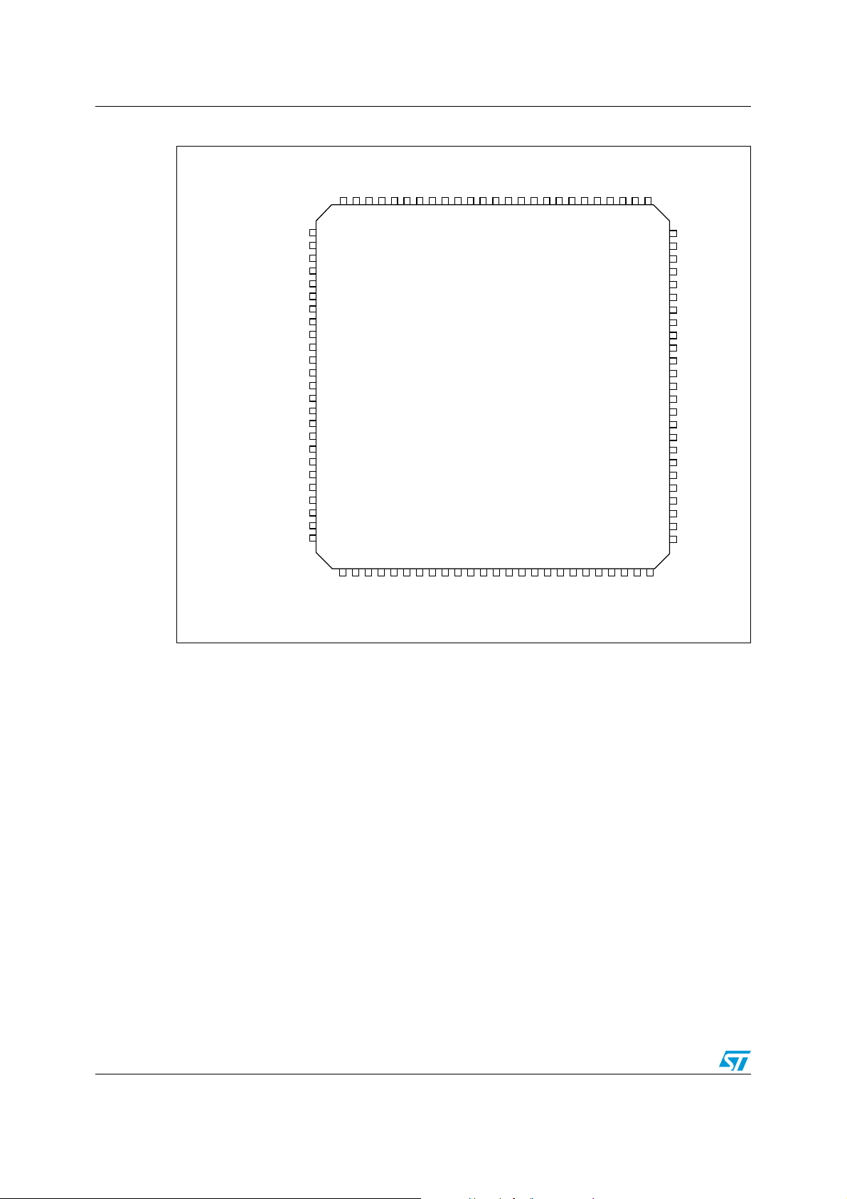
Figure 3. STM32F103xx performance line LFBGA100 ballout . . . . . . . . . . . . . . . . . . . . . . . . . . . . . 21
Figure 4. STM32F103xx performance line LQFP100 pinout . . . . . . . . . . . . . . . . . . . . . . . . . . . . . . . 22
Figure 5. STM32F103xx performance line LQFP64 pinout . . . . . . . . . . . . . . . . . . . . . . . . . . . . . . . . 23
Figure 6. STM32F103xx performance line TFBGA64 ballout . . . . . . . . . . . . . . . . . . . . . . . . . . . . . . 24
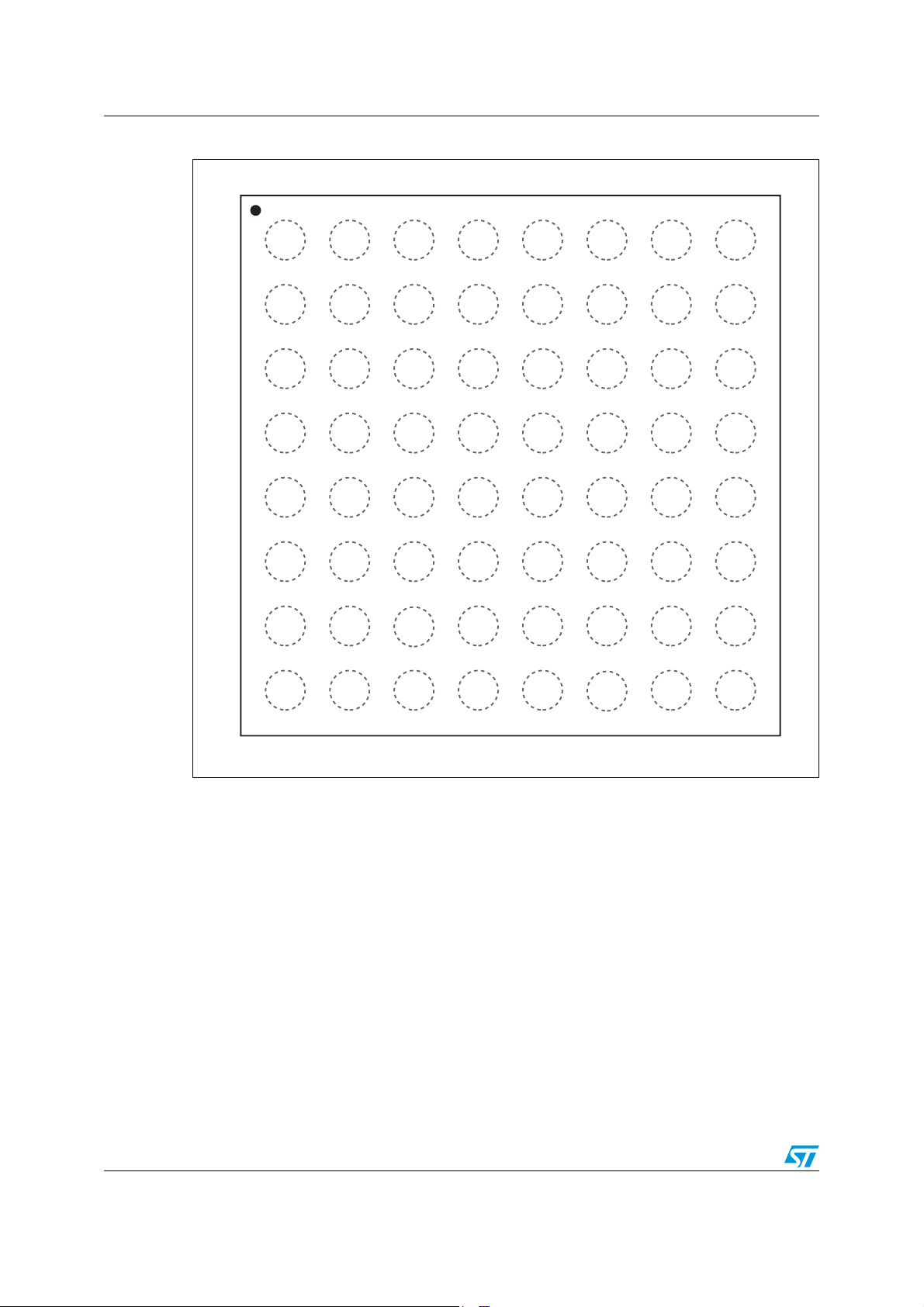
Figure 7. STM32F103xx performance line LQFP48 pinout . . . . . . . . . . . . . . . . . . . . . . . . . . . . . . . . 25
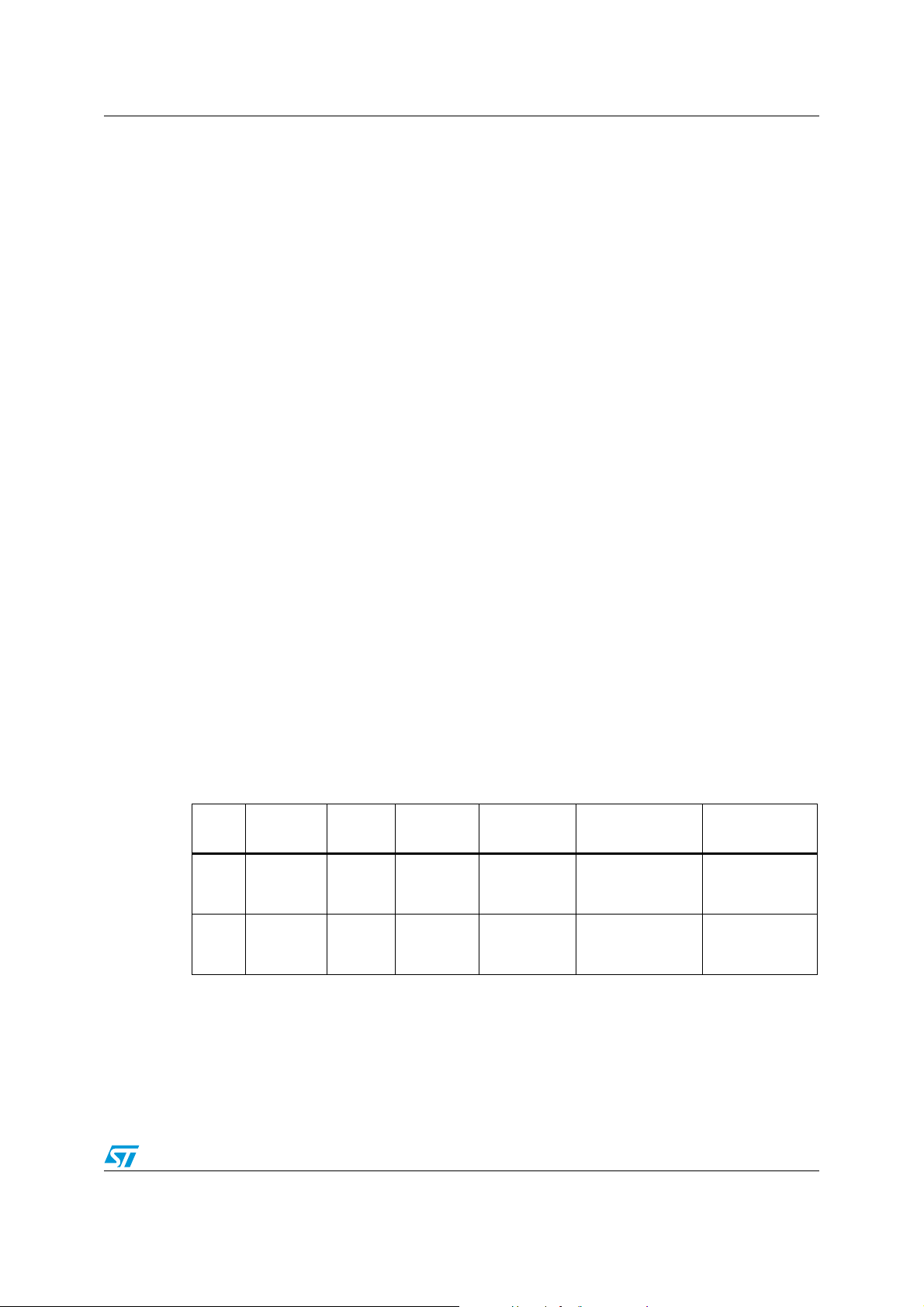
Figure 8. STM32F103xx performance line VFQFPN48 pinout . . . . . . . . . . . . . . . . . . . . . . . . . . . . . 25
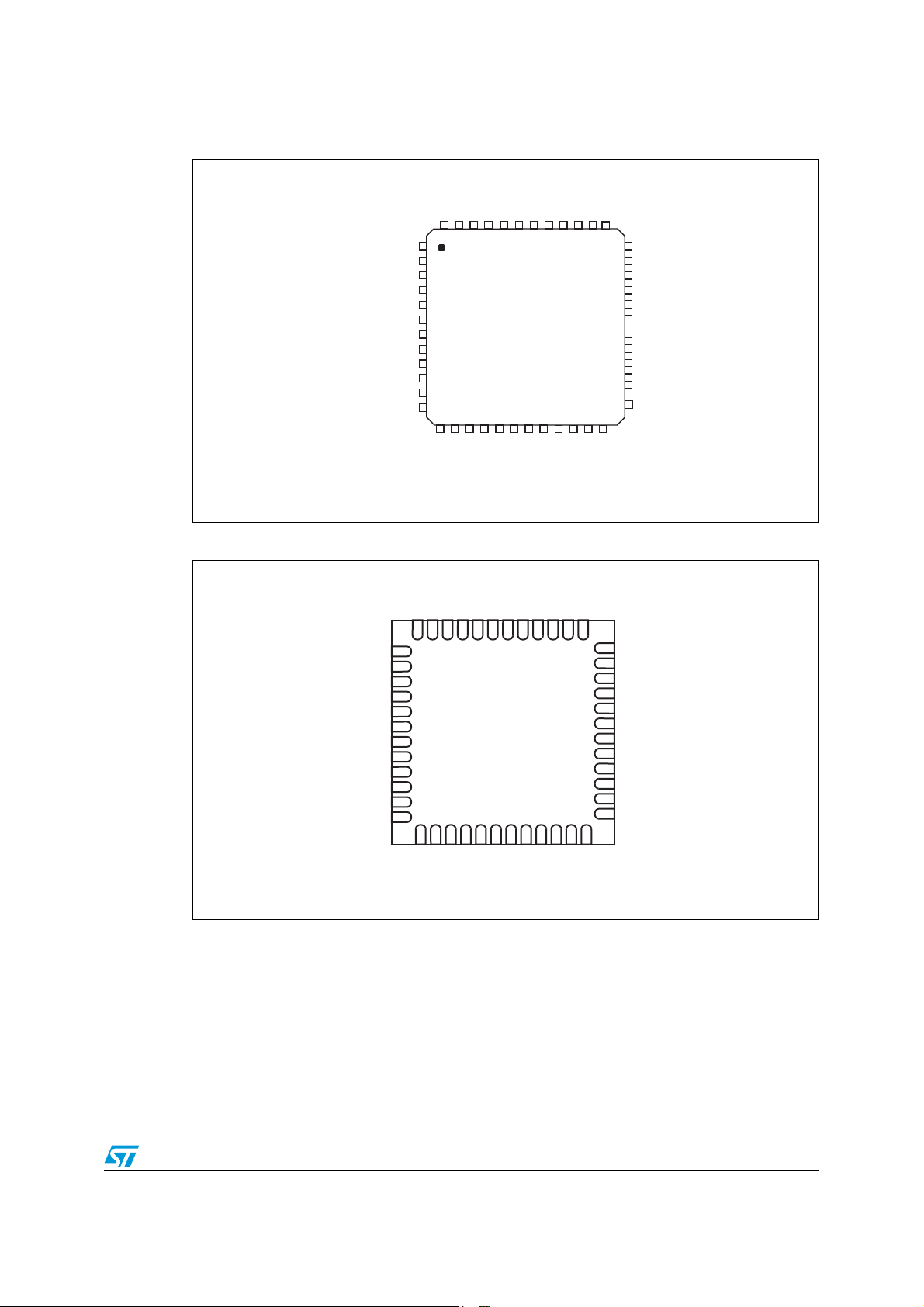
Figure 9. STM32F103xx performance line VFQFPN36 pinout . . . . . . . . . . . . . . . . . . . . . . . . . . . . . 26
Figure 10. Memory map . . . . . . . . . . . . . . . . . . . . . . . . . . . . . . . . . . . . . . . . . . . . . . . . . . . . . . . . . . . . 32
Figure 11. Pin loading conditions . . . . . . . . . . . . . . . . . . . . . . . . . . . . . . . . . . . . . . . . . . . . . . . . . . . . . 34
Figure 12. Pin input voltage . . . . . . . . . . . . . . . . . . . . . . . . . . . . . . . . . . . . . . . . . . . . . . . . . . . . . . . . . 34
Figure 13. Power supply scheme. . . . . . . . . . . . . . . . . . . . . . . . . . . . . . . . . . . . . . . . . . . . . . . . . . . . . 34
Figure 14. Current consumption measurement scheme . . . . . . . . . . . . . . . . . . . . . . . . . . . . . . . . . . . 35
Figure 15. Typical current consumption in Run mode versus frequency (at 3.6 V) -
code with data processing running from RAM, peripherals enabled. . . . . . . . . . . . . . . . . . 41
Figure 16. Typical current consumption in Run mode versus frequency (at 3.6 V) -
code with data processing running from RAM, peripherals disabled . . . . . . . . . . . . . . . . . 41
Figure 17. Typical current consumption on V
V
values . . . . . . . . . . . . . . . . . . . . . . . . . . . . . . . . . . . . . . . . . . . . . . . . . . . . . . . . . . . . 43
BAT
Figure 18. Typical current consumption in Stop mode with regulator in Run mode versus
temperature at V
= 3.3 V and 3.6 V . . . . . . . . . . . . . . . . . . . . . . . . . . . . . . . . . . . . . . . . 44
DD
Figure 19. Typical current consumption in Stop mode with regulator in Low-power mode versus
temperature at V
= 3.3 V and 3.6 V . . . . . . . . . . . . . . . . . . . . . . . . . . . . . . . . . . . . . . . . 44
DD
Figure 20. Typical current consumption in Standby mode versus temperature at
V
= 3.3 V and 3.6 V . . . . . . . . . . . . . . . . . . . . . . . . . . . . . . . . . . . . . . . . . . . . . . . . . . . . 45
DD
Figure 21. High-speed external clock source AC timing diagram . . . . . . . . . . . . . . . . . . . . . . . . . . . . 50
Figure 22. Low-speed external clock source AC timing diagram . . . . . . . . . . . . . . . . . . . . . . . . . . . . . 50
Figure 23. Typical application with an 8 MHz crystal . . . . . . . . . . . . . . . . . . . . . . . . . . . . . . . . . . . . . . 51
Figure 24. Typical application with a 32.768 kHz crystal . . . . . . . . . . . . . . . . . . . . . . . . . . . . . . . . . . . 53
Figure 25. Standard I/O input characteristics - CMOS port . . . . . . . . . . . . . . . . . . . . . . . . . . . . . . . . . 61
Figure 26. Standard I/O input characteristics - TTL port . . . . . . . . . . . . . . . . . . . . . . . . . . . . . . . . . . . 61
Figure 27. 5 V tolerant I/O input characteristics - CMOS port . . . . . . . . . . . . . . . . . . . . . . . . . . . . . . . 62
Figure 28. 5 V tolerant I/O input characteristics - TTL port . . . . . . . . . . . . . . . . . . . . . . . . . . . . . . . . . 62
Figure 29. I/O AC characteristics definition . . . . . . . . . . . . . . . . . . . . . . . . . . . . . . . . . . . . . . . . . . . . . 65
Figure 30. Recommended NRST pin protection . . . . . . . . . . . . . . . . . . . . . . . . . . . . . . . . . . . . . . . . . 66
Figure 31. I
2
C bus AC waveforms and measurement circuit . . . . . . . . . . . . . . . . . . . . . . . . . . . . . . . . 68
Figure 32. SPI timing diagram - slave mode and CPHA = 0 . . . . . . . . . . . . . . . . . . . . . . . . . . . . . . . . 70
Figure 33. SPI timing diagram - slave mode and CPHA = 1
Figure 34. SPI timing diagram - master mode
Figure 35. USB timings: definition of data signal rise and fall time . . . . . . . . . . . . . . . . . . . . . . . . . . . 72
Figure 36. ADC accuracy characteristics. . . . . . . . . . . . . . . . . . . . . . . . . . . . . . . . . . . . . . . . . . . . . . . 75
Figure 37. Typical connection diagram using the ADC . . . . . . . . . . . . . . . . . . . . . . . . . . . . . . . . . . . . 76
Figure 38. Power supply and reference decoupling (V
Figure 39. Power supply and reference decoupling (V
Figure 40. VFQFPN36 6 x 6 mm, 0.5 mm pitch, package outline
Figure 41. Recommended footprint (dimensions in mm)
Figure 42. VFQFPN48 7 x 7 mm, 0.5 mm pitch, package outline
with RTC on versus temperature at different
BAT
(1)
(1)
. . . . . . . . . . . . . . . . . . . . . . . . . . . . . . . . . . . . . . . . . 71
REF+
REF+
. . . . . . . . . . . . . . . . . . . . . . . . . . . . . . 70
not connected to V
connected to V
(1) . . . . . . . . . . . . . . . . . . . . . . . . . . . . . . . . . . 79
(1)(2) . . . . . . . . . . . . . . . . . . . . . . . . . . . . . . . . . . . . . . . . 79
(1) . . . . . . . . . . . . . . . . . . . . . . . . . . . . . . . . . . 80
DDA
). . . . . . . . . . . . . . 76
DDA
). . . . . . . . . . . . . . . . . 77
Doc ID 13587 Rev 13 7/99

List of figures STM32F103x8, STM32F103xB
Figure 43. Recommended footprint (dimensions in mm)
(1)(2) . . . . . . . . . . . . . . . . . . . . . . . . . . . . . . . . . . . . . . . . 80
Figure 44. LFBGA100 - 10 x 10 mm low profile fine pitch ball grid array package
outline . . . . . . . . . . . . . . . . . . . . . . . . . . . . . . . . . . . . . . . . . . . . . . . . . . . . . . . . . . . . . . . . . 81
Figure 45. Recommended PCB design rules (0.80/0.75 mm pitch BGA) . . . . . . . . . . . . . . . . . . . . . . 82
Figure 46. LQFP100, 14 x 14 mm 100-pin low-profile quad flat package outline . . . . . . . . . . . . . . . . 83
Figure 47. Recommended footprint
Figure 48. LQFP64, 10 x 10 mm, 64-pin low-profile quad flat package outline . . . . . . . . . . . . . . . . . . 84
Figure 49. Recommended footprint
(1)
. . . . . . . . . . . . . . . . . . . . . . . . . . . . . . . . . . . . . . . . . . . . . . . . . 83
(1)
. . . . . . . . . . . . . . . . . . . . . . . . . . . . . . . . . . . . . . . . . . . . . . . . . 84
Figure 50. TFBGA64 - 8 x 8 active ball array, 5 x 5 mm, 0.5 mm pitch, package outline . . . . . . . . . . 85
Figure 51. Recommended PCB design rules for pads (0.5 mm pitch BGA) . . . . . . . . . . . . . . . . . . . . 86
Figure 52. LQFP48, 7 x 7 mm, 48-pin low-profile quad flat package outline . . . . . . . . . . . . . . . . . . . . 87
Figure 53. Recommended footprint
Figure 54. LQFP100 P
max vs. TA . . . . . . . . . . . . . . . . . . . . . . . . . . . . . . . . . . . . . . . . . . . . . . . . . . 90
D
(1)
. . . . . . . . . . . . . . . . . . . . . . . . . . . . . . . . . . . . . . . . . . . . . . . . . 87
8/99 Doc ID 13587 Rev 13

STM32F103x8, STM32F103xB Introduction
1 Introduction
This datasheet provides the ordering information and mechanical device characteristics of
the STM32F103x8 and STM32F103xB medium-density performance line microcontrollers.
For more details on the whole STMicroelectronics STM32F103xx family, please refer to
Section 2.2: Full compatibility throughout the family.
The medium-density STM32F103xx datasheet should be read in conjunction with the low-,
medium- and high-density STM32F10xxx reference manual.
The reference and Flash programming manuals are both available from the
STMicroelectronics website www.st.com.
For information on the Cortex™-M3 core please refer to the Cortex™-M3 Technical
Reference Manual, available from the www.arm.com website at the following address:
http://infocenter.arm.com/help/index.jsp?topic=/com.arm.doc.ddi0337e/.
2 Description
The STM32F103xx medium-density performance line family incorporates the highperformance ARM Cortex™-M3 32-bit RISC core operating at a 72 MHz frequency, highspeed embedded memories (Flash memory up to 128 Kbytes and SRAM up to 20 Kbytes),
and an extensive range of enhanced I/Os and peripherals connected to two APB buses. All
devices offer two 12-bit ADCs, three general purpose 16-bit timers plus one PWM timer, as
well as standard and advanced communication interfaces: up to two I
USARTs, an USB and a CAN.
The devices operate from a 2.0 to 3.6 V power supply. They are available in both the –40 to
+85 °C temperature range and the –40 to +105 °C extended temperature range. A
comprehensive set of power-saving mode allows the design of low-power applications.
The STM32F103xx medium-density performance line family includes devices in six different
package types: from 36 pins to 100 pins. Depending on the device chosen, different sets of
peripherals are included, the description below gives an overview of the complete range of
peripherals proposed in this family.
These features make the STM32F103xx medium-density performance line microcontroller
family suitable for a wide range of applications such as motor drives, application control,
medical and handheld equipment, PC and gaming peripherals, GPS platforms, industrial
applications, PLCs, inverters, printers, scanners, alarm systems, video intercoms, and
HVACs.
2
Cs and SPIs, three
Doc ID 13587 Rev 13 9/99
Description STM32F103x8, STM32F103xB
2.1 Device overview
Table 2. STM32F103xx medium-density device features and peripheral counts
Peripheral
Flash - Kbytes 64 128 64 128 64 128 64 128
SRAM - Kbytes 20 20 20 20
General-purpose 33 3 3
Advanced-control 11 1 1
Timers
SPI 12 2 2
2
I
C 12 2 2
USART 23 3 3
USB 11 1 1
Communication
CAN 11 1 1
GPIOs 26 37 51 80
STM32F103Tx STM32F103Cx STM32F103Rx
STM32F103Vx
12-bit synchronized ADC
Number of channels
CPU frequency 72 MHz
Operating voltage 2.0 to 3.6 V
Operating temperatures
Packages VFQFPN36
2
10 channels
Ambient temperatures: –40 to +85 °C /–40 to +105 °C (see Ta bl e 9 )
Junction temperature: –40 to + 125 °C (see Ta bl e 9 )
2
10 channels
LQFP48,
VFQFPN48
16 channels
2
LQFP64,
TFBGA64
2
16 channels
LQFP100,
LFBGA100
10/99 Doc ID 13587 Rev 13
STM32F103x8, STM32F103xB Description
USBDP/CA N_TX
PA[15: 0]
EXTI
WWDG
12bit ADC1
16AF
JTDI
JTCK/ SWCLK
JTMS/SWDIO
NJTRSTTRST
JTDO
NRST
V
DD
= 2 to 3.6V
80AF
PB[15: 0]
PC[15:0 ]
AHB2
MOSI,MISO,SCK,NSS
SRAM
2x(8x16bit)
WAKEUP
GPIOA
GPIOB
GPIOC
F
max
: 72 M
Hz
V
SS
SCL,SDA
I2C2
V
REF+
GP DMA
TIM2
TIM3
XTAL OSC
4-16 MHz
XTAL 32 kHz
OSC_IN
OSC_OUT
OSC32_OUT
OSC32_IN
PLL &
APB1 : F
max
=24 / 36 MHz
PCLK1
HCLK
CLOCK
MANA GT
PCLK2
as AF
as AF
Flash 128 KB
VOLT. REG.
3.3V TO 1.8V
POWER
Backu p i nterf ace
as AF
TIM 4
BusM atrix
64 bit
Interface
20 KB
RTC
RC 8 MHz
Cortex-M3 CPU
Ibus
Dbus
pbu s
obl
flash
SRAM 512B
Trace
Cont roller
USART1
USART2
SPI2
bxCAN
7 channels
Back up
reg
4 Chann els
TIM1
3 com pl. Chann els
SCL,SDA ,SMBA
I2C1
as AF
RX,TX, CTS, RTS,
USART3
Temp sens or
V
REF-
PD[15: 0]
GPIOD
PE[15: 0]
GPIOE
AHB:F
max
=48/72 MHz
ETR and BKIN
4 Chann els
4 Chann els
4 Chann els
FCLK
RC 40 kHz
Stand by
IWDG
@VBAT
POR / PDR
SUPPLY
@VDDA
VDDA
VSSA
@VDDA
V
BAT
RX,TX, CTS, RTS,
Smart Card as AF
RX,TX, CTS, RTS,
CK, SmartCard as AF
APB2 : F
max
=48 / 72 MHz
NVIC
SPI1
MOSI,MISO,
SCK,NSS as AF
12bit ADC2
IF
IFIF
int erface
@VDDA
SUPERVISION
PVD
Rst
Int
@VDD
AHB2
APB2
APB 1
AWU
TAMPER-RTC
@VDD
USB 2.0 FS
USBDM/CAN_RX
System
ai14390d
TRACECLK
TRACED[0:3]
as AS
SW/JTAG
TPIU
Trace/trig
CK, SmartCard as AF
Figure 1. STM32F103xx performance line block diagram
1. TA = –40 °C to +105 °C (junction temperature up to 125 °C).
2. AF = alternate function on I/O port pin.
Doc ID 13587 Rev 13 11/99
Description STM32F103x8, STM32F103xB
HSE OSC
4-16 MHz
OSC_IN
OSC_OUT
OSC32_IN
OSC32_OUT
LSE OSC
32.768 kHz
HSI RC
8 MHz
LSI RC
40 kHz
to Independent Watchdog (IWDG)
PLL
x2, x3, x4
PLLMUL
Legend:
MCO
Clock Output
Main
PLLXTPRE
/2
..., x16
AHB
Prescaler
/1, 2..512
/2
PLLCLK
HSI
HSE
APB1
Prescaler
/1, 2, 4, 8, 16
ADC
Prescaler
/2, 4, 6, 8
ADCCLK
PCLK1
HCLK
PLLCLK
to AHB bus, core,
memory and DMA
USBCLK
to USB interface
to TIM2, 3
and 4
USB
Prescaler
/1, 1.5
to ADC
LSE
LSI
HSI
/128
/2
HSI
HSE
peripherals
to APB1
Peripheral Clock
Enable (13 bits)
Enable (3 bits)
P
eripheral Clock
APB2
Prescaler
/1, 2, 4, 8, 16
PCLK2
to TIM1
peripherals
to APB2
Peripheral Clock
Enable (11 bits)
Enable (1 bit)
Peripheral Clock
48 MHz
72 MHz max
72 MHz
72 MHz max
36 MHz max
to RTC
PLLSRC
SW
MCO
CSS
to Cortex System timer
/8
Clock
Enable (3 bits)
SYSCLK
max
RTCCLK
RTCSEL[1:0]
TIM1CLK
TIMXCLK
IWDGCLK
SYSCLK
FCLK Cortex
free running clock
TIM2,3, 4
If (APB1 prescaler =1) x1
else x2
TIM1 timer
If (APB2 prescaler =1) x1
else x2
HSE = high-speed external clock signal
HSI = high-speed internal clock signal
LSI = low-speed internal clock signal
LSE = low-speed external clock signal
ai14903
FLITFCLK
to Flash programming interface
Figure 2. Clock tree
1. When the HSI is used as a PLL clock input, the maximum system clock frequency that can be achieved is
64 MHz.
2. For the USB function to be available, both HSE and PLL must be enabled, with USBCLK running at 48
MHz.
3. To have an ADC conversion time of 1 µs, APB2 must be at 14 MHz, 28 MHz or 56 MHz.
12/99 Doc ID 13587 Rev 13
STM32F103x8, STM32F103xB Description
2.2 Full compatibility throughout the family
The STM32F103xx is a complete family whose members are fully pin-to-pin, software and
feature compatible. In the reference manual, the STM32F103x4 and STM32F103x6 are
identified as low-density devices, the STM32F103x8 and STM32F103xB are referred to as
medium-density devices, and the STM32F103xC, STM32F103xD and STM32F103xE are
referred to as high-density devices.
Low- and high-density devices are an extension of the STM32F103x8/B devices, they are
specified in the STM32F103x4/6 and STM32F103xC/D/E datasheets, respectively. Lowdensity devices feature lower Flash memory and RAM capacities, less timers and
peripherals. High-density devices have higher Flash memory and RAM capacities, and
additional peripherals like SDIO, FSMC, I
the other members of the STM32F103xx family.
The STM32F103x4, STM32F103x6, STM32F103xC, STM32F103xD and STM32F103xE
are a drop-in replacement for STM32F103x8/B medium-density devices, allowing the user
to try different memory densities and providing a greater degree of freedom during the
development cycle.
Moreover, the STM32F103xx performance line family is fully compatible with all existing
STM32F101xx access line and STM32F102xx USB access line devices.
Table 3. STM32F103xx family
2
S and DAC, while remaining fully compatible with
Low-density devices Medium-density devices High-density devices
Pinout
144
100
64
48
36
1. For orderable part numbers that do not show the A internal code after the temperature range code (6 or 7),
the reference datasheet for electrical characteristics is that of the STM32F103x8/B medium-density
devices.
16 KB
Flash
6 KB RAM 10 KB RAM 20 KB RAM 20 KB RAM 48 KB RAM 64 KB RAM 64 KB RAM
2 × USARTs
2 × 16-bit timers
1 × SPI, 1 × I
CAN, 1 × PWM timer
2 × ADCs
32 KB
Flash
2
C, USB,
(1)
64 KB
Flash
3 × USARTs
3 × 16-bit timers
2 × SPIs, 2 × I
CAN, 1 × PWM timer
2 × ADCs
128 KB
Flash
2
Cs, USB,
256 KB
Flash
5 × USARTs
4 × 16-bit timers, 2 × basic timers
3 × SPIs, 2 × I
USB, CAN, 2 × PWM timers
3 × ADCs, 2 × DACs, 1 × SDIO
FSMC (100 and 144 pins)
384 KB
Flash
2
Ss, 2 × I2Cs
512 KB
Flash
Doc ID 13587 Rev 13 13/99

Description STM32F103x8, STM32F103xB
2.3 Overview
2.3.1 ARM® Cortex™-M3 core with embedded Flash and SRAM
The ARM Cortex™-M3 processor is the latest generation of ARM processors for embedded
systems. It has been developed to provide a low-cost platform that meets the needs of MCU
implementation, with a reduced pin count and low-power consumption, while delivering
outstanding computational performance and an advanced system response to interrupts.
The ARM Cortex™-M3 32-bit RISC processor features exceptional code-efficiency,
delivering the high-performance expected from an ARM core in the memory size usually
associated with 8- and 16-bit devices.
The STM32F103xx performance line family having an embedded ARM core, is therefore
compatible with all ARM tools and software.
Figure 1 shows the general block diagram of the device family.
2.3.2 Embedded Flash memory
64 or 128 Kbytes of embedded Flash is available for storing programs and data.
2.3.3 CRC (cyclic redundancy check) calculation unit
The CRC (cyclic redundancy check) calculation unit is used to get a CRC code from a 32-bit
data word and a fixed generator polynomial.
Among other applications, CRC-based techniques are used to verify data transmission or
storage integrity. In the scope of the EN/IEC 60335-1 standard, they offer a means of
verifying the Flash memory integrity. The CRC calculation unit helps compute a signature of
the software during runtime, to be compared with a reference signature generated at linktime and stored at a given memory location.
2.3.4 Embedded SRAM
Twenty Kbytes of embedded SRAM accessed (read/write) at CPU clock speed with 0 wait
states.
2.3.5 Nested vectored interrupt controller (NVIC)
The STM32F103xx performance line embeds a nested vectored interrupt controller able to
handle up to 43 maskable interrupt channels (not including the 16 interrupt lines of
Cortex™-M3) and 16 priority levels.
● Closely coupled NVIC gives low-latency interrupt processing
● Interrupt entry vector table address passed directly to the core
● Closely coupled NVIC core interface
● Allows early processing of interrupts
● Processing of late arriving higher priority interrupts
● Support for tail-chaining
● Processor state automatically saved
● Interrupt entry restored on interrupt exit with no instruction overhead
14/99 Doc ID 13587 Rev 13

STM32F103x8, STM32F103xB Description
This hardware block provides flexible interrupt management features with minimal interrupt
latency.
2.3.6 External interrupt/event controller (EXTI)
The external interrupt/event controller consists of 19 edge detector lines used to generate
interrupt/event requests. Each line can be independently configured to select the trigger
event (rising edge, falling edge, both) and can be masked independently. A pending register
maintains the status of the interrupt requests. The EXTI can detect an external line with a
pulse width shorter than the Internal APB2 clock period. Up to 80 GPIOs can be connected
to the 16 external interrupt lines.
2.3.7 Clocks and startup
System clock selection is performed on startup, however the internal RC 8 MHz oscillator is
selected as default CPU clock on reset. An external 4-16 MHz clock can be selected, in
which case it is monitored for failure. If failure is detected, the system automatically switches
back to the internal RC oscillator. A software interrupt is generated if enabled. Similarly, full
interrupt management of the PLL clock entry is available when necessary (for example on
failure of an indirectly used external crystal, resonator or oscillator).
Several prescalers allow the configuration of the AHB frequency, the high-speed APB
(APB2) and the low-speed APB (APB1) domains. The maximum frequency of the AHB and
the high-speed APB domains is 72 MHz. The maximum allowed frequency of the low-speed
APB domain is 36 MHz. See Figure 2 for details on the clock tree.
2.3.8 Boot modes
At startup, boot pins are used to select one of three boot options:
● Boot from User Flash
● Boot from System Memory
● Boot from embedded SRAM
The boot loader is located in System Memory. It is used to reprogram the Flash memory by
using USART1. For further details please refer to AN2606.
2.3.9 Power supply schemes
● V
● V
● V
For more details on how to connect power pins, refer to Figure 13: Power supply scheme.
= 2.0 to 3.6 V: external power supply for I/Os and the internal regulator.
DD
Provided externally through V
, V
SSA
= 2.0 to 3.6 V: external analog power supplies for ADC, reset blocks, RCs
DDA
and PLL (minimum voltage to be applied to V
V
and V
DDA
= 1.8 to 3.6 V: power supply for RTC, external clock 32 kHz oscillator and backup
BAT
must be connected to V
SSA
registers (through power switch) when V
2.3.10 Power supply supervisor
The device has an integrated power-on reset (POR)/power-down reset (PDR) circuitry. It is
always active, and ensures proper operation starting from/down to 2 V. The device remains
DD
pins.
is 2.4 V when the ADC is used).
DDA
and VSS, respectively.
DD
is not present.
DD
Doc ID 13587 Rev 13 15/99

Description STM32F103x8, STM32F103xB
in reset mode when V
external reset circuit.
The device features an embedded programmable voltage detector (PVD) that monitors the
V
DD/VDDA
generated when V
than the V
power supply and compares it to the V
DD/VDDA
threshold. The interrupt service routine can then generate a warning
PVD
message and/or put the MCU into a safe state. The PVD is enabled by software.
Refer to Table 11: Embedded reset and power control block characteristics for the values of
V
POR/PDR
and V
PVD
.
2.3.11 Voltage regulator
The regulator has three operation modes: main (MR), low power (LPR) and power down.
● MR is used in the nominal regulation mode (Run)
● LPR is used in the Stop mode
● Power down is used in Standby mode: the regulator output is in high impedance: the
kernel circuitry is powered down, inducing zero consumption (but the contents of the
registers and SRAM are lost)
This regulator is always enabled after reset. It is disabled in Standby mode, providing high
impedance output.
2.3.12 Low-power modes
is below a specified threshold, V
DD
drops below the V
PVD
threshold and/or when VDD/V
PVD
POR/PDR
, without the need for an
threshold. An interrupt can be
is higher
DDA
The STM32F103xx performance line supports three low-power modes to achieve the best
compromise between low power consumption, short startup time and available wakeup
sources:
● Sleep mode
In Sleep mode, only the CPU is stopped. All peripherals continue to operate and can
wake up the CPU when an interrupt/event occurs.
● Stop mode
The Stop mode achieves the lowest power consumption while retaining the content of
SRAM and registers. All clocks in the 1.8 V domain are stopped, the PLL, the HSI RC
and the HSE crystal oscillators are disabled. The voltage regulator can also be put
either in normal or in low power mode.
The device can be woken up from Stop mode by any of the EXTI line. The EXTI line
source can be one of the 16 external lines, the PVD output, the RTC alarm or the USB
wakeup.
● Standby mode
The Standby mode is used to achieve the lowest power consumption. The internal
voltage regulator is switched off so that the entire 1.8 V domain is powered off. The
PLL, the HSI RC and the HSE crystal oscillators are also switched off. After entering
Standby mode, SRAM and register contents are lost except for registers in the Backup
domain and Standby circuitry.
The device exits Standby mode when an external reset (NRST pin), an IWDG reset, a
rising edge on the WKUP pin, or an RTC alarm occurs.
Note: The RTC, the IWDG, and the corresponding clock sources are not stopped by entering Stop
or Standby mode.
16/99 Doc ID 13587 Rev 13
STM32F103x8, STM32F103xB Description
2.3.13 DMA
The flexible 7-channel general-purpose DMA is able to manage memory-to-memory,
peripheral-to-memory and memory-to-peripheral transfers. The DMA controller supports
circular buffer management avoiding the generation of interrupts when the controller
reaches the end of the buffer.
Each channel is connected to dedicated hardware DMA requests, with support for software
trigger on each channel. Configuration is made by software and transfer sizes between
source and destination are independent.
The DMA can be used with the main peripherals: SPI, I
2
C, USART, general-purpose and
advanced-control timers TIMx and ADC.
2.3.14 RTC (real-time clock) and backup registers
The RTC and the backup registers are supplied through a switch that takes power either on
V
supply when present or through the V
DD
registers used to store 20 bytes of user application data when V
The real-time clock provides a set of continuously running counters which can be used with
suitable software to provide a clock calendar function, and provides an alarm interrupt and a
periodic interrupt. It is clocked by a 32.768 kHz external crystal, resonator or oscillator, the
internal low-power RC oscillator or the high-speed external clock divided by 128. The
internal low-power RC has a typical frequency of 40 kHz. The RTC can be calibrated using
an external 512 Hz output to compensate for any natural crystal deviation. The RTC features
a 32-bit programmable counter for long-term measurement using the Compare register to
generate an alarm. A 20-bit prescaler is used for the time base clock and is by default
configured to generate a time base of 1 second from a clock at 32.768 kHz.
pin. The backup registers are ten 16-bit
BAT
power is not present.
DD
2.3.15 Timers and watchdogs
The medium-density STM32F103xx performance line devices include an advanced-control
timer, three general-purpose timers, two watchdog timers and a SysTick timer.
Ta bl e 4 compares the features of the advanced-control and general-purpose timers.
Table 4. Timer feature comparison
Timer
TIM1 16-bit
TIM2,
TIM3,
TIM4
Counter
resolution
16-bit
Counter
type
Up,
down,
up/down
Up,
down,
up/down
Prescaler
factor
Any integer
between 1
and 65536
Any integer
between 1
and 65536
DMA request
generation
Ye s 4 Ye s
Ye s 4 N o
Capture/compare
channels
Complementary
outputs
Doc ID 13587 Rev 13 17/99

Description STM32F103x8, STM32F103xB
Advanced-control timer (TIM1)
The advanced-control timer (TIM1) can be seen as a three-phase PWM multiplexed on 6
channels. It has complementary PWM outputs with programmable inserted dead-times. It
can also be seen as a complete general-purpose timer. The 4 independent channels can be
used for
● Input capture
● Output compare
● PWM generation (edge- or center-aligned modes)
● One-pulse mode output
If configured as a general-purpose 16-bit timer, it has the same features as the TIMx timer. If
configured as the 16-bit PWM generator, it has full modulation capability (0-100%).
In debug mode, the advanced-control timer counter can be frozen and the PWM outputs
disabled to turn off any power switch driven by these outputs.
Many features are shared with those of the general-purpose TIM timers which have the
same architecture. The advanced-control timer can therefore work together with the TIM
timers via the Timer Link feature for synchronization or event chaining.
General-purpose timers (TIMx)
There are up to three synchronizable general-purpose timers embedded in the
STM32F103xx performance line devices. These timers are based on a 16-bit auto-reload
up/down counter, a 16-bit prescaler and feature 4 independent channels each for input
capture/output compare, PWM or one-pulse mode output. This gives up to 12 input
captures/output compares/PWMs on the largest packages.
The general-purpose timers can work together with the advanced-control timer via the Timer
Link feature for synchronization or event chaining. Their counter can be frozen in debug
mode. Any of the general-purpose timers can be used to generate PWM outputs. They all
have independent DMA request generation.
These timers are capable of handling quadrature (incremental) encoder signals and the
digital outputs from 1 to 3 hall-effect sensors.
Independent watchdog
The independent watchdog is based on a 12-bit downcounter and 8-bit prescaler. It is
clocked from an independent 40 kHz internal RC and as it operates independently of the
main clock, it can operate in Stop and Standby modes. It can be used either as a watchdog
to reset the device when a problem occurs, or as a free-running timer for application timeout
management. It is hardware- or software-configurable through the option bytes. The counter
can be frozen in debug mode.
Window watchdog
The window watchdog is based on a 7-bit downcounter that can be set as free-running. It
can be used as a watchdog to reset the device when a problem occurs. It is clocked from the
main clock. It has an early warning interrupt capability and the counter can be frozen in
debug mode.
18/99 Doc ID 13587 Rev 13

STM32F103x8, STM32F103xB Description
SysTick timer
This timer is dedicated for OS, but could also be used as a standard downcounter. It
features:
● A 24-bit downcounter
● Autoreload capability
● Maskable system interrupt generation when the counter reaches 0
● Programmable clock source
2.3.16 I²C bus
Up to two I²C bus interfaces can operate in multimaster and slave modes. They can support
standard and fast modes.
They support dual slave addressing (7-bit only) and both 7/10-bit addressing in master
mode. A hardware CRC generation/verification is embedded.
They can be served by DMA and they support SM Bus 2.0/PM Bus.
2.3.17 Universal synchronous/asynchronous receiver transmitter (USART)
One of the USART interfaces is able to communicate at speeds of up to 4.5 Mbit/s. The
other available interfaces communicate at up to 2.25 Mbit/s. They provide hardware
management of the CTS and RTS signals, IrDA SIR ENDEC support, are ISO 7816
compliant and have LIN Master/Slave capability.
All USART interfaces can be served by the DMA controller.
2.3.18 Serial peripheral interface (SPI)
Up to two SPIs are able to communicate up to 18 Mbits/s in slave and master modes in fullduplex and simplex communication modes. The 3-bit prescaler gives 8 master mode
frequencies and the frame is configurable to 8 bits or 16 bits. The hardware CRC
generation/verification supports basic SD Card/MMC modes.
Both SPIs can be served by the DMA controller.
2.3.19 Controller area network (CAN)
The CAN is compliant with specifications 2.0A and B (active) with a bit rate up to 1 Mbit/s. It
can receive and transmit standard frames with 11-bit identifiers as well as extended frames
with 29-bit identifiers. It has three transmit mailboxes, two receive FIFOs with 3 stages and
14 scalable filter banks.
2.3.20 Universal serial bus (USB)
The STM32F103xx performance line embeds a USB device peripheral compatible with the
USB full-speed 12 Mbs. The USB interface implements a full-speed (12 Mbit/s) function
interface. It has software-configurable endpoint setting and suspend/resume support. The
dedicated 48 MHz clock is generated from the internal main PLL (the clock source must use
a HSE crystal oscillator).
Doc ID 13587 Rev 13 19/99

Description STM32F103x8, STM32F103xB
2.3.21 GPIOs (general-purpose inputs/outputs)
Each of the GPIO pins can be configured by software as output (push-pull or open-drain), as
input (with or without pull-up or pull-down) or as peripheral alternate function. Most of the
GPIO pins are shared with digital or analog alternate functions. All GPIOs are high-currentcapable except for analog inputs.
The I/Os alternate function configuration can be locked if needed following a specific
sequence in order to avoid spurious writing to the I/Os registers.
I/Os on APB2 with up to 18 MHz toggling speed
2.3.22 ADC (analog-to-digital converter)
Two 12-bit analog-to-digital converters are embedded into STM32F103xx performance line
devices and each ADC shares up to 16 external channels, performing conversions in singleshot or scan modes. In scan mode, automatic conversion is performed on a selected group
of analog inputs.
Additional logic functions embedded in the ADC interface allow:
● Simultaneous sample and hold
● Interleaved sample and hold
● Single shunt
The ADC can be served by the DMA controller.
An analog watchdog feature allows very precise monitoring of the converted voltage of one,
some or all selected channels. An interrupt is generated when the converted voltage is
outside the programmed thresholds.
The events generated by the general-purpose timers (TIMx) and the advanced-control timer
(TIM1) can be internally connected to the ADC start trigger, injection trigger, and DMA
trigger respectively, to allow the application to synchronize A/D conversion and timers.
2.3.23 Temperature sensor
The temperature sensor has to generate a voltage that varies linearly with temperature. The
conversion range is between 2 V < V
< 3.6 V. The temperature sensor is internally
DDA
connected to the ADC12_IN16 input channel which is used to convert the sensor output
voltage into a digital value.
2.3.24 Serial wire JTAG debug port (SWJ-DP)
The ARM SWJ-DP Interface is embedded. and is a combined JTAG and serial wire debug
port that enables either a serial wire debug or a JTAG probe to be connected to the target.
The JTAG TMS and TCK pins are shared with SWDIO and SWCLK, respectively, and a
specific sequence on the TMS pin is used to switch between JTAG-DP and SW-DP.
20/99 Doc ID 13587 Rev 13

STM32F103x8, STM32F103xB Pinouts and pin description
AI16001c
PE10
PC14-
OSC32_IN
PC5PA5
PC3
PB4
PE15
PB2
PC4PA4
H
PE14
PE11PE7
D PD4
PD3
PB8PE3
C
PD0
PC12
PE5
PB5
PC0
PE2
B PC11PD2
PC15-
OSC32_OUT
PB7
PB6
A
87654321
V
SS_5
OSC_IN
OSC_OUT V
DD_5
G
F
E
PC1
V
REF–
PC13-
TAMPER-RTC
PB9
PA15
PB3
PE4
PE1
PE0
V
SS_1
PD1PE6NRST
PC2
V
SS_3
V
SS_4
NCV
DD_3
V
DD_4
PB15
V
BAT
PD5
PD6
BOOT0 PD7
V
SS_2
V
SSA
PA1
V
DD_2
V
DD_1
PB14
PA0-WKUP
109
K
J
PD10
PD11
PA8
PA9
PA10
PA11
PA12
PC10
PA13
PA14
PC9
PC7
PC6
PD15
PC8
PD14
PE12
PB1PA7
PB11
PE8
PB0PA6
PB10
PE13PE9V
DDA
PB13
V
REF+
PA3
PB12
PA2
PD8
PD9 PD13
PD12
3 Pinouts and pin description
Figure 3. STM32F103xx performance line LFBGA100 ballout
Doc ID 13587 Rev 13 21/99
Pinouts and pin description STM32F103x8, STM32F103xB
100999897969594939291908988878685848382818079787776
1
2
3
4
5
6
7
8
9
10
11
12
13
14
15
16
17
18
19
20
21
22
23
24
25
75
74
73
72
71
70
69
68
67
66
65
64
63
62
61
60
59
58
57
56
55
54
53
52
51
VDD_2
VSS_2
NC
PA 1 3
PA 1 2
PA 1 1
PA 1 0
PA 9
PA 8
PC9
PC8
PC7
PC6
PD15
PD14
PD13
PD12
PD11
PD10
PD9
PD8
PB15
PB14
PB13
PB12
PA 3
VSS_4
VDD_4
PA 4
PA 5
PA 6
PA 7
PC4
PC5
PB0
PB1
PB2
PE7
PE8
PE9
PE10
PE11
PE12
PE13
PE14
PE15
PB10
PB11
VSS_1
VDD_1
VDD_3
VSS_3
PE1
PE0
PB9
PB8
BOOT0
PB7
PB6
PB5
PB4
PB3
PD7
PD6
PD5
PD4
PD3
PD2
PD1
PD0
PC12
PC11
PC10
PA15
PA14
26272829303132333435363738394041424344454647484950
PE2
PE3
PE4
PE5
PE6
VBAT
PC13-TAMPER-RTC
PC14-OSC32_IN
PC15-OSC32_OUT
VSS_5
VDD_5
OSC_IN
OSC_OUT
NRST
PC0
PC1
PC2
PC3
VSSA
VREF-
VREF+
VDDA
PA 0- W K UP
PA 1
PA 2
ai14391
LQFP100
Figure 4. STM32F103xx performance line LQFP100 pinout
22/99 Doc ID 13587 Rev 13

STM32F103x8, STM32F103xB Pinouts and pin description
64 63 62 61 60 59 58 57 56 55 54 53 52 51 50 49
48
47
46
45
44
43
42
41
40
39
38
37
36
35
34
33
17 18 19 20 21 22 23 24 29 30 31 3225 26 27 28
1
2
3
4
5
6
7
8
9
10
11
12
13
14
15
16
VBAT
PC13-TAMPER-RTC
PC14-OSC32_IN
PC15-OSC32_OUT
PD0 OSC_IN
PD1 OSC_OUT
NRST
PC0
PC1
PC2
PC3
VSSA
VDDA
PA 0- W K UP
PA 1
PA 2
VDD_3
VSS_3
PB9
PB8
BOOT0
PB7
PB6
PB5
PB4
PB3
PD2
PC12
PC11
PC10
PA 1 5
PA 14
VDD_2
VSS_2
PA 1 3
PA 1 2
PA 1 1
PA 1 0
PA 9
PA 8
PC9
PC8
PC7
PC6
PB15
PB14
PB13
PB12
PA 3
VSS_4
VDD_4
PA 4
PA 5
PA 6
PA 7
PC4
PC5
PB0
PB1
PB2
PB10
PB11
VSS_1
VDD_1
LQFP64
ai14392
Figure 5. STM32F103xx performance line LQFP64 pinout
Doc ID 13587 Rev 13 23/99
Pinouts and pin description STM32F103x8, STM32F103xB
AI15494
PB2
PC14-
OSC32_IN
PA7PA4
PA2
PA15
PB11
PB1PA6PA3
H
PB10
PC5PC4
D PA8
PA9
BOOT0PB8
C
PC9
PA11
PB6
PC12
V
DDA
PB9
B
PA12
PC10
PC15-
OSC32_OUT
PB3
PD2
A
87654321
V
SS_4
OSC_IN
OSC_OUT V
DD_4
G
F
E
PC2
V
REF+
PC13-
TAMPER-RTC
PB4 PA13PA14
PB7
PB5
V
SS_3
PC7 PC8PC0NRST PC1
PB0PA5 PB14
V
DD_2
V
DD_3
PB13
V
BAT
PC11
PA10
V
SS_2
V
SS_1
PC6V
SSA
PA1
V
DD_1
PB15
PB12
PA0-WKUP
Figure 6. STM32F103xx performance line TFBGA64 ballout
24/99 Doc ID 13587 Rev 13
STM32F103x8, STM32F103xB Pinouts and pin description
ai18300
VDD_3
VSS_3
PB9
PB8
BOOT0
PB7
PB6
PB5
PB4
PB3
PA15
PA14
PA 3
PA 4
PA 5
PA 6
PA 7
PB0
PB1
PB2
PB10
PB11
VSS_1
VDD_1
VBAT
PC13-TAMPER-RTC
PC14-OSC32_IN
PC15-OSC32_OUT
PD0-OSC_IN
PD1-OSC_OUT
NRST
VSSA
VDDA
PA0-WKUP
PA 1
PA 2
VDD_2
VSS_2
PA13
PA12
PA11
PA10
PA 9
PA 8
PB15
PB14
PB13
PB12
48
VFQFPN48
47 46
45 444342 41
40 39 38 37
36
35
34
33
32
31
30
29
28
27
26
25
13
14 15
16 171819 20
21 22 23 24
1
2
3
4
5
6
7
8
9
10
11
12
Figure 7. STM32F103xx performance line LQFP48 pinout
VDD_3
VSS_3
PB9
PB8
BOOT0
PB7
PB6
PB5
PB4
PB3
PA1 5
PA 14
PC13-TAMPER-RTC
VBAT
PC14-OSC32_IN
PC15-OSC32_OUT
PD0-OSC_IN
PD1-OSC_OUT
NRST
VSSA
VDDA
PA 0- W K UP
PA 1
PA 2
48 47 46 45
1
2
3
4
5
6
7
8
9
10
11
12
13 14 15 16 17 18 19 20 21 22
PA 3
44 43 42 41 40 39 38 37
LQFP48
PA 4
PA 5
PA 6
PA 7
PB0
PB1
PB2
VDD_2
36
VSS_2
35
PA1 3
34
PA1 2
33
PA1 1
32
PA1 0
31
PA9
30
PA8
29
PB15
28
27
PB14
26
PB13
25
PB12
24
23
PB10
PB11
VSS_1
VDD_1
ai14393b
Figure 8. STM32F103xx performance line VFQFPN48 pinout
Doc ID 13587 Rev 13 25/99
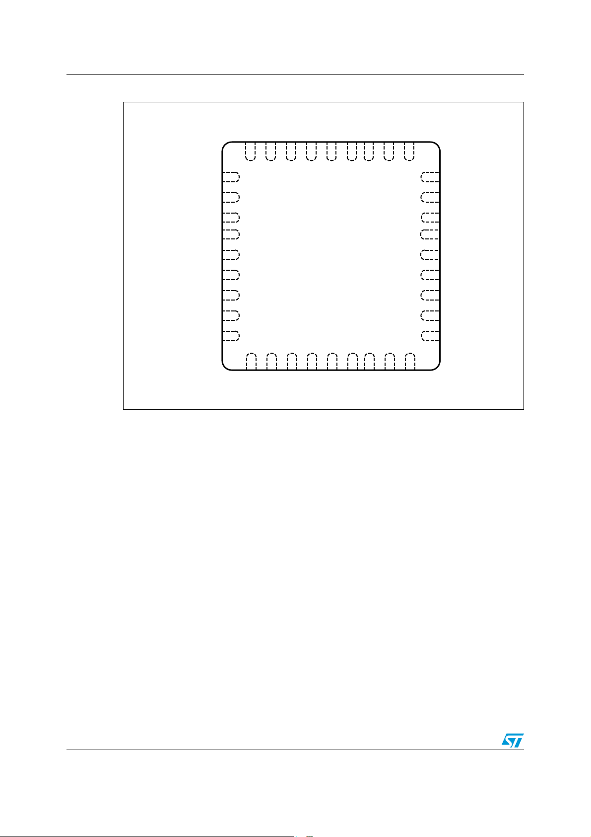
Pinouts and pin description STM32F103x8, STM32F103xB
V
SS_3
BOOT0
PB7
PB6
PB5
PB4
PB3
PA15
PA14
36 35 34 33 32 31 30 29 28
V
DD_3
1
27
V
DD_2
OSC_IN/PD0
2
26
V
SS_2
OSC_OUT/PD1
3
25
PA13
NRST
4
QFN36
24
PA12
V
SSA
5
23 PA11
V
DDA
6
22
PA10
PA0-WKUP
7
21
PA 9
PA 1
8
20
PA 8
PA 2 9
19
V
DD_1
10 11 12 13 14 15 16 17 18
PA 3
PA 4
PA 5
PA 6
PA 7
PB0
PB1
PB2
V
SS_1
ai14654
Figure 9. STM32F103xx performance line VFQFPN36 pinout
26/99 Doc ID 13587 Rev 13
STM32F103x8, STM32F103xB Pinouts and pin description
Table 5. Medium-density STM32F103xx pin definitions
LFBGA100
Pins
LQFP64
TFBGA64
LQFP100
Pin name
VFQFPN36
(1)
Type
(2)
Main
function
(after reset)
I / O Level
(3)
Alternate functions
Default Remap
LQFP48/VFQFPN48
A3 - - 1 - PE2 I/O FT PE2 TRACECK
B3 - - 2 - PE3 I/O FT PE3 TRACED0
C3 - - 3 - PE4 I/O FT PE4 TRACED1
D3 - - 4 - PE5 I/O FT PE5 TRACED2
E3 - - 5 - PE6 I/O FT PE6 TRACED3
B2 1 B2 1 6 - V
A2 2 A2 2 7 -
BAT
PC13-TAMPER-
RTC
(5)
A1 3 A1 3 8 - PC14-OSC32_IN
B1 4 B1 4 9 -
C2---10- V
D2---11- V
PC15-
OSC32_OUT
SS_5
DD_5
SV
I/O PC13
(5)
I/O PC14
I/O PC15
(5)
SV
SV
BAT
SS_5
DD_5
(6)
(6)
(6)
TAMPER-RTC
OSC32_IN
OSC32_OUT
C1 5 C1 5 12 2 OSC_IN I OSC_IN
D1 6 D1 6 13 3 OSC_OUT O OSC_OUT
E1 7 E1 7 14 4 NRST I/O NRST
F1 - E3 8 15 - PC0 I/O PC0 ADC12_IN10
F2 - E2 9 16 - PC1 I/O PC1 ADC12_IN11
E2 - F2 10 17 - PC2 I/O PC2 ADC12_IN12
F3 - -
G1 8 F1 12 19 5 V
H1---20- V
J1 - G1
K1 9 H1 13 22 6 V
(7)
11 18 - PC3 I/O PC3 ADC12_IN13
SV
SV
SV
SV
SSA
REF-
REF+
DDA
(7)
-21- V
SSA
REF-
REF+
DDA
WKUP/
G2 10 G2 14 23 7 PA0-WKUP I/O PA0
USART2_CTS
ADC12_IN0/
TIM2_CH1_ETR
USART2_RTS
H2 11 H2 15 24 8 PA1 I/O PA1
ADC12_IN1/
TIM2_CH2
(8)
(8)
(8)
(4)
/
(8)
/
Doc ID 13587 Rev 13 27/99
Pinouts and pin description STM32F103x8, STM32F103xB
Table 5. Medium-density STM32F103xx pin definitions (continued)
(4)
LFBGA100
Pins
TFBGA64
Alternate functions
(2)
Pin name
(1)
Type
LQFP64
LQFP100
VFQFPN36
Main
function
(after reset)
I / O Level
(3)
Default Remap
LQFP48/VFQFPN48
(8)
(8)
(8)
(8)
(8)
(8)
/
/
/
/
J2 12 F3 16 25 9 PA2 I/O PA2
K2 13 G3 17 26 10 PA3 I/O PA3
E4 - C2 18 27 - V
F4 - D2 19 28 - V
SS_4
DD_4
SV
SV
SS_4
DD_4
G3 14 H3 20 29 11 PA4 I/O PA4
USART2_TX
ADC12_IN2/
TIM2_CH3
USART2_RX
ADC12_IN3/
TIM2_CH4
SPI1_NSS
USART2_CK
ADC12_IN4
H3 15 F4 21 30 12 PA5 I/O PA5
J3 16 G4 22 31 13 PA6 I/O PA6
K3 17 H4 23 32 14 PA7 I/O PA7
SPI1_SCK
ADC12_IN5
SPI1_MISO
ADC12_IN6/
TIM3_CH1
SPI1_MOSI
ADC12_IN7/
TIM3_CH2
(8)
(8)
(8)
(8)
(8)
/
/
TIM1_BKIN
/
TIM1_CH1N
G4 - H5 24 33 PC4 I/O PC4 ADC12_IN14
H4 - H6 25 34 PC5 I/O PC5 ADC12_IN15
J4 18 F5 26 35 15 PB0 I/O PB0
K4 19 G5 27 36 16 PB1 I/O PB1
ADC12_IN8/
TIM3_CH3
ADC12_IN9/
TIM3_CH4
(8)
(8)
TIM1_CH2N
TIM1_CH3N
G5 20 G6 28 37 17 PB2 I/O FT PB2/BOOT1
H5 - - - 38 - PE7 I/O FT PE7 TIM1_ETR
J5 - - - 39 - PE8 I/O FT PE8 TIM1_CH1N
K5 - - - 40 - PE9 I/O FT PE9 TIM1_CH1
G6 - - - 41 - PE10 I/O FT PE10 TIM1_CH2N
H6 - - - 42 - PE11 I/O FT PE11 TIM1_CH2
J6 - - - 43 - PE12 I/O FT PE12 TIM1_CH3N
K6 - - - 44 - PE13 I/O FT PE13 TIM1_CH3
G7 - - - 45 - PE14 I/O FT PE14 TIM1_CH4
28/99 Doc ID 13587 Rev 13
STM32F103x8, STM32F103xB Pinouts and pin description
Table 5. Medium-density STM32F103xx pin definitions (continued)
(4)
TIM2_CH3
TIM2_CH4
TIM4_CH1 /
USART3_RTS
LFBGA100
Pins
TFBGA64
(2)
Pin name
(1)
Type
LQFP64
LQFP100
VFQFPN36
Main
function
(after reset)
I / O Level
(3)
Alternate functions
Default Remap
LQFP48/VFQFPN48
H7 - - - 46 - PE15 I/O FT PE15 TIM1_BKIN
J7 21 G7 29 47 - PB10 I/O FT PB10
K7 22 H7 30 48 - PB11 I/O FT PB11
E7 23 D6 31 49 18 V
F7 24 E6 32 50 19 V
SS_1
DD_1
SV
SV
SS_1
DD_1
I2C2_SCL/
USART3_TX
I2C2_SDA/
USART3_RX
(8)
(8)
SPI2_NSS/
K8 25 H8 33 51 - PB12 I/O FT PB12
J8 26 G8 34 52 - PB13 I/O FT PB13
H8 27 F8 35 53 - PB14 I/O FT PB14
G8 28 F7 36 54 - PB15 I/O FT PB15
I2C2_SMBAl/
USART3_CK
TIM1_BKIN
SPI2_SCK/
USART3_CTS
TIM1_CH1N
SPI2_MISO/
USART3_RTS
TIM1_CH2N
SPI2_MOSI/
TIM1_CH3N
(8)
(8)
(8)
(8)
(8)
(8)
(8)
/
/
K9 - - - 55 - PD8 I/O FT PD8 USART3_TX
J9 - - - 56 - PD9 I/O FT PD9 USART3_RX
H9 - - - 57 - PD10 I/O FT PD10 USART3_CK
G9 - - - 58 - PD11 I/O FT PD11 USART3_CTS
K10 - - - 59 - PD12 I/O FT PD12
J10 - - - 60 - PD13 I/O FT PD13 TIM4_CH2
H10 - - - 61 - PD14 I/O FT PD14 TIM4_CH3
G10 - - - 62 - PD15 I/O FT PD15 TIM4_CH4
F10 - F6 37 63 - PC6 I/O FT PC6 TIM3_CH1
E10 E7 38 64 - PC7 I/O FT PC7 TIM3_CH2
F9 E8 39 65 - PC8 I/O FT PC8 TIM3_CH3
E9 - D8 40 66 - PC9 I/O FT PC9 TIM3_CH4
D9 29 D7 41 67 20 PA8 I/O FT PA8
USART1_CK/
TIM1_CH1
(8)
/MCO
Doc ID 13587 Rev 13 29/99
Pinouts and pin description STM32F103x8, STM32F103xB
Table 5. Medium-density STM32F103xx pin definitions (continued)
(4)
LFBGA100
Pins
TFBGA64
Alternate functions
(2)
Pin name
(1)
Type
LQFP64
LQFP100
VFQFPN36
Main
function
(after reset)
I / O Level
(3)
Default Remap
LQFP48/VFQFPN48
(8)
C9 30 C7 42 68 21 PA9 I/O FT PA9
D1031C6436922 PA10 I/OFT PA10
C1032C8447023 PA11 I/OFT PA11
B1033B8457124 PA12 I/OFT PA12
USART1_TX
TIM1_CH2
USART1_RX
TIM1_CH3
USART1_CTS/
CANRX
(8)
TIM1_CH4
USART1_RTS/
CANTX
(8)
TIM1_ETR
/
(8)
(8)
/
(8)
/ USBDM
(8)
//USBDP
(8)
A10 34 A8 46 72 25 PA13 I/O FT JTMS/SWDIO PA13
F8 - - - 73 - Not connected
E6 35 D5 47 74 26 V
F6 36 E5 48 75 27 V
SS_2
DD_2
SV
SV
SS_2
DD_2
A9 37 A7 49 76 28 PA14 I/O FT JTCK/SWCLK PA14
A8 38 A6 50 77 29 PA15 I/O FT JTDI
TIM2_CH1_ETR/
PA 1 5 / S P I 1_ N S S
B9 - B7 51 78 PC10 I/O FT PC10 USART3_TX
B8 - B6 52 79 PC11 I/O FT PC11 USART3_RX
C8 - C5 53 80 PC12 I/O FT PC12 USART3_CK
D8 5 C1 5 81 2 PD0 I/O FT OSC_IN
E8 6 D1 6 82 3 PD1 I/O FT OSC_OUT
(9)
(9)
CANRX
CANTX
B7 B5 54 83 - PD2 I/O FT PD2 TIM3_ETR
C7 - - - 84 - PD3 I/O FT PD3 USART2_CTS
D7 - - - 85 - PD4 I/O FT PD4 USART2_RTS
B6 - - - 86 - PD5 I/O FT PD5 USART2_TX
C6 - - - 87 - PD6 I/O FT PD6 USART2_RX
D6 - - - 88 - PD7 I/O FT PD7 USART2_CK
TIM2_CH2 / PB3
A7 39 A5 55 89 30 PB3 I/O FT JTDO
TRACESWO
SPI1_SCK
A6 40 A4 56 90 31 PB4 I/O FT JNTRST
TIM3_CH1/ PB4/
SPI1_MISO
30/99 Doc ID 13587 Rev 13
 Loading...