


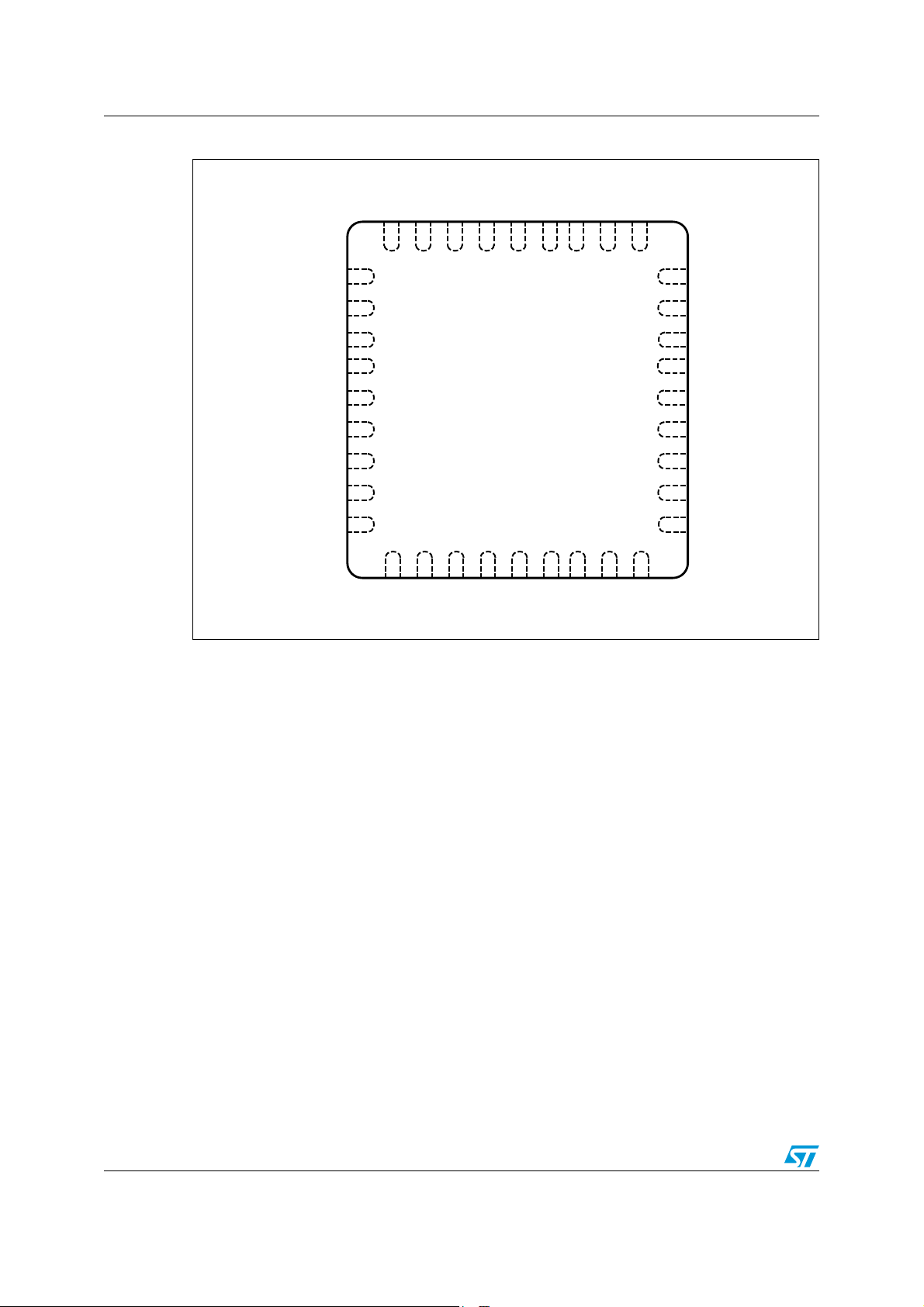
STM32F103x8
BGA100 10 × 10 mm
BGA64 5 × 5 mm
VFQFPN48 7 × 7 mm
VFQFPN36 6 × 6 mm
LQFP100 14 × 14 m
LQFP64 10 × 10 m
LQFP48 7 × 7 m
STM32F103xB
Medium-density performance line ARM-based 32-bit MCU with 64 or
128 KB Flash, USB, CAN, 7 timers, 2 ADCs, 9 communication interfaces
Features
■ ARM 32-bit Cortex™-M3 CPU Core
– 72 MHz maximum frequency,
1.25 DMIPS/MHz (Dhrystone 2.1)
performance at 0 wait state memory
access
– Single-cycle multiplication and hardware
division
■ Memories
– 64 or 128 Kbytes of Flash memory
– 20 Kbytes of SRAM
■ Clock, reset and supply management
– 2.0 to 3.6 V application supply and I/Os
– POR, PDR, and programmable voltage
detector (PVD)
– 4-to-16 MHz crystal oscillator
– Internal 8 MHz factory-trimmed RC
– Internal 40 kHz RC
– PLL for CPU clock
– 32 kHz oscillator for RTC with calibration
■ Low power
– Sleep, Stop and Standby modes
–V
■ 2 x 12-bit, 1 µs A/D converters (up to 16
supply for RTC and backup registers
BAT
channels)
– Conversion range: 0 to 3.6 V
– Dual-sample and hold capability
– Temperature sensor
■ DMA
– 7-channel DMA controller
– Peripherals supported: timers, ADC, SPIs,
2
I
Cs and USARTs
■ Up to 80 fast I/O ports
– 26/37/51/80 I/Os, all mappable on 16
external interrupt vectors and almost all
5 V-tolerant
■ Debug mode
– Serial wire debug (SWD) & JTAG interfaces
■ 7 timers
– Three 16-bit timers, each with up to 4
IC/OC/PWM or pulse counter and
quadrature (incremental) encoder input
– 16-bit, motor control PWM timer with dead-
time generation and emergency stop
– 2 watchdog timers (Independent and
Window)
– SysTick timer 24-bit downcounter
■ Up to 9 communication interfaces
– Up to 2 x I
2
C interfaces (SMBus/PMBus)
– Up to 3 USARTs (ISO 7816 interface, LIN,
IrDA capability, modem control)
– Up to 2 SPIs (18 Mbit/s)
– CAN interface (2.0B Active)
– USB 2.0 full-speed interface
■ CRC calculation unit, 96-bit unique ID
■ Packages are ECOPACK
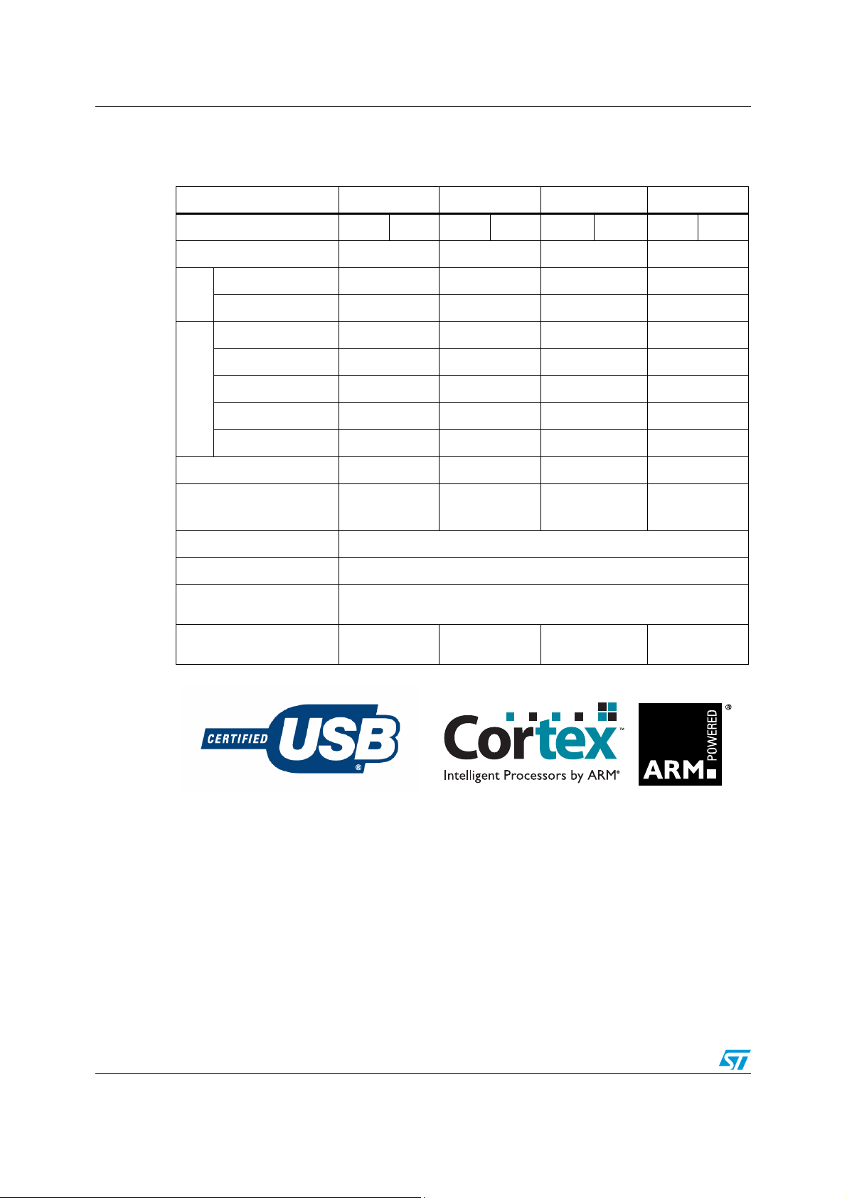
Table 1. Device summary
Reference Part number
STM32F103x8
STM32F103xB
STM32F103C8, STM32F103R8
STM32F103V8, STM32F103T8
STM32F103RB STM32F103VB,
STM32F103CB, STM32F103TB
®
April 2011 Doc ID 13587 Rev 13 1/99
www.st.com
1

Contents STM32F103x8, STM32F103xB
Contents
1 Introduction . . . . . . . . . . . . . . . . . . . . . . . . . . . . . . . . . . . . . . . . . . . . . . . . 9
2 Description . . . . . . . . . . . . . . . . . . . . . . . . . . . . . . . . . . . . . . . . . . . . . . . . . 9
2.1 Device overview . . . . . . . . . . . . . . . . . . . . . . . . . . . . . . . . . . . . . . . . . . . . 10
2.2 Full compatibility throughout the family . . . . . . . . . . . . . . . . . . . . . . . . . . 13
2.3 Overview . . . . . . . . . . . . . . . . . . . . . . . . . . . . . . . . . . . . . . . . . . . . . . . . . 14
2.3.1 ARM® Cortex™-M3 core with embedded Flash and SRAM . . . . . . . . . 14
2.3.2 Embedded Flash memory . . . . . . . . . . . . . . . . . . . . . . . . . . . . . . . . . . . 14
2.3.3 CRC (cyclic redundancy check) calculation unit . . . . . . . . . . . . . . . . . . 14
2.3.4 Embedded SRAM . . . . . . . . . . . . . . . . . . . . . . . . . . . . . . . . . . . . . . . . . 14
2.3.5 Nested vectored interrupt controller (NVIC) . . . . . . . . . . . . . . . . . . . . . . 14
2.3.6 External interrupt/event controller (EXTI) . . . . . . . . . . . . . . . . . . . . . . . 15
2.3.7 Clocks and startup . . . . . . . . . . . . . . . . . . . . . . . . . . . . . . . . . . . . . . . . . 15
2.3.8 Boot modes . . . . . . . . . . . . . . . . . . . . . . . . . . . . . . . . . . . . . . . . . . . . . . 15
2.3.9 Power supply schemes . . . . . . . . . . . . . . . . . . . . . . . . . . . . . . . . . . . . . 15
2.3.10 Power supply supervisor . . . . . . . . . . . . . . . . . . . . . . . . . . . . . . . . . . . . 15
2.3.11 Voltage regulator . . . . . . . . . . . . . . . . . . . . . . . . . . . . . . . . . . . . . . . . . . 16
2.3.12 Low-power modes . . . . . . . . . . . . . . . . . . . . . . . . . . . . . . . . . . . . . . . . . 16
2.3.13 DMA . . . . . . . . . . . . . . . . . . . . . . . . . . . . . . . . . . . . . . . . . . . . . . . . . . . . 17
2.3.14 RTC (real-time clock) and backup registers . . . . . . . . . . . . . . . . . . . . . . 17
2.3.15 Timers and watchdogs . . . . . . . . . . . . . . . . . . . . . . . . . . . . . . . . . . . . . . 17
2.3.16 I²C bus . . . . . . . . . . . . . . . . . . . . . . . . . . . . . . . . . . . . . . . . . . . . . . . . . . 19
2.3.17 Universal synchronous/asynchronous receiver transmitter (USART) . . 19
2.3.18 Serial peripheral interface (SPI) . . . . . . . . . . . . . . . . . . . . . . . . . . . . . . . 19
2.3.19 Controller area network (CAN) . . . . . . . . . . . . . . . . . . . . . . . . . . . . . . . 19
2.3.20 Universal serial bus (USB) . . . . . . . . . . . . . . . . . . . . . . . . . . . . . . . . . . . 19
2.3.21 GPIOs (general-purpose inputs/outputs) . . . . . . . . . . . . . . . . . . . . . . . . 20
2.3.22 ADC (analog-to-digital converter) . . . . . . . . . . . . . . . . . . . . . . . . . . . . . 20
2.3.23 Temperature sensor . . . . . . . . . . . . . . . . . . . . . . . . . . . . . . . . . . . . . . . . 20
2.3.24 Serial wire JTAG debug port (SWJ-DP) . . . . . . . . . . . . . . . . . . . . . . . . . 20
3 Pinouts and pin description . . . . . . . . . . . . . . . . . . . . . . . . . . . . . . . . . . 21
4 Memory mapping . . . . . . . . . . . . . . . . . . . . . . . . . . . . . . . . . . . . . . . . . . 32
2/99 Doc ID 13587 Rev 13

STM32F103x8, STM32F103xB Contents
5 Electrical characteristics . . . . . . . . . . . . . . . . . . . . . . . . . . . . . . . . . . . . 33
5.1 Parameter conditions . . . . . . . . . . . . . . . . . . . . . . . . . . . . . . . . . . . . . . . . 33
5.1.1 Minimum and maximum values . . . . . . . . . . . . . . . . . . . . . . . . . . . . . . . 33
5.1.2 Typical values . . . . . . . . . . . . . . . . . . . . . . . . . . . . . . . . . . . . . . . . . . . . . 33
5.1.3 Typical curves . . . . . . . . . . . . . . . . . . . . . . . . . . . . . . . . . . . . . . . . . . . . 33
5.1.4 Loading capacitor . . . . . . . . . . . . . . . . . . . . . . . . . . . . . . . . . . . . . . . . . 33
5.1.5 Pin input voltage . . . . . . . . . . . . . . . . . . . . . . . . . . . . . . . . . . . . . . . . . . 33
5.1.6 Power supply scheme . . . . . . . . . . . . . . . . . . . . . . . . . . . . . . . . . . . . . . 34
5.1.7 Current consumption measurement . . . . . . . . . . . . . . . . . . . . . . . . . . . 35
5.2 Absolute maximum ratings . . . . . . . . . . . . . . . . . . . . . . . . . . . . . . . . . . . . 35
5.3 Operating conditions . . . . . . . . . . . . . . . . . . . . . . . . . . . . . . . . . . . . . . . . 36
5.3.1 General operating conditions . . . . . . . . . . . . . . . . . . . . . . . . . . . . . . . . . 36
5.3.2 Operating conditions at power-up / power-down . . . . . . . . . . . . . . . . . . 37
5.3.3 Embedded reset and power control block characteristics . . . . . . . . . . . 37
5.3.4 Embedded reference voltage . . . . . . . . . . . . . . . . . . . . . . . . . . . . . . . . . 39
5.3.5 Supply current characteristics . . . . . . . . . . . . . . . . . . . . . . . . . . . . . . . . 39
5.3.6 External clock source characteristics . . . . . . . . . . . . . . . . . . . . . . . . . . . 49
5.3.7 Internal clock source characteristics . . . . . . . . . . . . . . . . . . . . . . . . . . . 53
5.3.8 PLL characteristics . . . . . . . . . . . . . . . . . . . . . . . . . . . . . . . . . . . . . . . . 55
5.3.9 Memory characteristics . . . . . . . . . . . . . . . . . . . . . . . . . . . . . . . . . . . . . 55
5.3.10 EMC characteristics . . . . . . . . . . . . . . . . . . . . . . . . . . . . . . . . . . . . . . . . 56
5.3.11 Absolute maximum ratings (electrical sensitivity) . . . . . . . . . . . . . . . . . 58
5.3.12 I/O current injection characteristics . . . . . . . . . . . . . . . . . . . . . . . . . . . . 59
5.3.13 I/O port characteristics . . . . . . . . . . . . . . . . . . . . . . . . . . . . . . . . . . . . . . 60
5.3.14 NRST pin characteristics . . . . . . . . . . . . . . . . . . . . . . . . . . . . . . . . . . . . 65
5.3.15 TIM timer characteristics . . . . . . . . . . . . . . . . . . . . . . . . . . . . . . . . . . . . 66
5.3.16 Communications interfaces . . . . . . . . . . . . . . . . . . . . . . . . . . . . . . . . . . 67
5.3.17 CAN (controller area network) interface . . . . . . . . . . . . . . . . . . . . . . . . . 72
5.3.18 12-bit ADC characteristics . . . . . . . . . . . . . . . . . . . . . . . . . . . . . . . . . . . 73
5.3.19 Temperature sensor characteristics . . . . . . . . . . . . . . . . . . . . . . . . . . . . 77
6 Package characteristics . . . . . . . . . . . . . . . . . . . . . . . . . . . . . . . . . . . . . 78
6.1 Package mechanical data . . . . . . . . . . . . . . . . . . . . . . . . . . . . . . . . . . . . 78
6.2 Thermal characteristics . . . . . . . . . . . . . . . . . . . . . . . . . . . . . . . . . . . . . . 88
6.2.1 Reference document . . . . . . . . . . . . . . . . . . . . . . . . . . . . . . . . . . . . . . . 88
6.2.2 Selecting the product temperature range . . . . . . . . . . . . . . . . . . . . . . . . 89
Doc ID 13587 Rev 13 3/99

Contents STM32F103x8, STM32F103xB
7 Ordering information scheme . . . . . . . . . . . . . . . . . . . . . . . . . . . . . . . . 91
8 Revision history . . . . . . . . . . . . . . . . . . . . . . . . . . . . . . . . . . . . . . . . . . . 92
4/99 Doc ID 13587 Rev 13

STM32F103x8, STM32F103xB List of tables
List of tables
Table 1. Device summary . . . . . . . . . . . . . . . . . . . . . . . . . . . . . . . . . . . . . . . . . . . . . . . . . . . . . . . . . . 1
Table 2. STM32F103xx medium-density device features and peripheral counts . . . . . . . . . . . . . . . 10
Table 3. STM32F103xx family . . . . . . . . . . . . . . . . . . . . . . . . . . . . . . . . . . . . . . . . . . . . . . . . . . . . . 13
Table 4. Timer feature comparison . . . . . . . . . . . . . . . . . . . . . . . . . . . . . . . . . . . . . . . . . . . . . . . . . . 17
Table 5. Medium-density STM32F103xx pin definitions . . . . . . . . . . . . . . . . . . . . . . . . . . . . . . . . . . 27
Table 6. Voltage characteristics . . . . . . . . . . . . . . . . . . . . . . . . . . . . . . . . . . . . . . . . . . . . . . . . . . . . 35
Table 7. Current characteristics . . . . . . . . . . . . . . . . . . . . . . . . . . . . . . . . . . . . . . . . . . . . . . . . . . . . 36
Table 8. Thermal characteristics. . . . . . . . . . . . . . . . . . . . . . . . . . . . . . . . . . . . . . . . . . . . . . . . . . . . 36
Table 9. General operating conditions . . . . . . . . . . . . . . . . . . . . . . . . . . . . . . . . . . . . . . . . . . . . . . . 36
Table 10. Operating conditions at power-up / power-down . . . . . . . . . . . . . . . . . . . . . . . . . . . . . . . . 37
Table 11. Embedded reset and power control block characteristics. . . . . . . . . . . . . . . . . . . . . . . . . . 38
Table 12. Embedded internal reference voltage . . . . . . . . . . . . . . . . . . . . . . . . . . . . . . . . . . . . . . . . . 39
Table 13. Maximum current consumption in Run mode, code with data processing
running from Flash . . . . . . . . . . . . . . . . . . . . . . . . . . . . . . . . . . . . . . . . . . . . . . . . . . . . . . . 40
Table 14. Maximum current consumption in Run mode, code with data processing
running from RAM. . . . . . . . . . . . . . . . . . . . . . . . . . . . . . . . . . . . . . . . . . . . . . . . . . . . . . . . 40
Table 15. Maximum current consumption in Sleep mode, code running from Flash or RAM. . . . . . . 42
Table 16. Typical and maximum current consumptions in Stop and Standby modes . . . . . . . . . . . . 43
Table 17. Typical current consumption in Run mode, code with data processing
running from Flash . . . . . . . . . . . . . . . . . . . . . . . . . . . . . . . . . . . . . . . . . . . . . . . . . . . . . . . 46
Table 18. Typical current consumption in Sleep mode, code running from Flash or
RAM . . . . . . . . . . . . . . . . . . . . . . . . . . . . . . . . . . . . . . . . . . . . . . . . . . . . . . . . . . . . . . . . . . 47
Table 19. Peripheral current consumption . . . . . . . . . . . . . . . . . . . . . . . . . . . . . . . . . . . . . . . . . . . . . 48
Table 20. High-speed external user clock characteristics. . . . . . . . . . . . . . . . . . . . . . . . . . . . . . . . . . 49
Table 21. Low-speed external user clock characteristics . . . . . . . . . . . . . . . . . . . . . . . . . . . . . . . . . . 49
Table 22. HSE 4-16 MHz oscillator characteristics . . . . . . . . . . . . . . . . . . . . . . . . . . . . . . . . . . . . . . 51
Table 23. LSE oscillator characteristics (f
Table 24. HSI oscillator characteristics. . . . . . . . . . . . . . . . . . . . . . . . . . . . . . . . . . . . . . . . . . . . . . . . 53
Table 25. LSI oscillator characteristics . . . . . . . . . . . . . . . . . . . . . . . . . . . . . . . . . . . . . . . . . . . . . . . 54
Table 26. Low-power mode wakeup timings . . . . . . . . . . . . . . . . . . . . . . . . . . . . . . . . . . . . . . . . . . . 55
Table 27. PLL characteristics . . . . . . . . . . . . . . . . . . . . . . . . . . . . . . . . . . . . . . . . . . . . . . . . . . . . . . . 55
Table 28. Flash memory characteristics . . . . . . . . . . . . . . . . . . . . . . . . . . . . . . . . . . . . . . . . . . . . . . . 55
Table 29. Flash memory endurance and data retention . . . . . . . . . . . . . . . . . . . . . . . . . . . . . . . . . . . 56
Table 30. EMS characteristics . . . . . . . . . . . . . . . . . . . . . . . . . . . . . . . . . . . . . . . . . . . . . . . . . . . . . . 57
Table 31. EMI characteristics . . . . . . . . . . . . . . . . . . . . . . . . . . . . . . . . . . . . . . . . . . . . . . . . . . . . . . . 57
Table 32. ESD absolute maximum ratings . . . . . . . . . . . . . . . . . . . . . . . . . . . . . . . . . . . . . . . . . . . . . 58
Table 33. Electrical sensitivities . . . . . . . . . . . . . . . . . . . . . . . . . . . . . . . . . . . . . . . . . . . . . . . . . . . . . 58
Table 34. I/O current injection susceptibility . . . . . . . . . . . . . . . . . . . . . . . . . . . . . . . . . . . . . . . . . . . . 59
Table 35. I/O static characteristics . . . . . . . . . . . . . . . . . . . . . . . . . . . . . . . . . . . . . . . . . . . . . . . . . . . 60
Table 36. Output voltage characteristics . . . . . . . . . . . . . . . . . . . . . . . . . . . . . . . . . . . . . . . . . . . . . . 63
Table 37. I/O AC characteristics . . . . . . . . . . . . . . . . . . . . . . . . . . . . . . . . . . . . . . . . . . . . . . . . . . . . . 64
Table 38. NRST pin characteristics . . . . . . . . . . . . . . . . . . . . . . . . . . . . . . . . . . . . . . . . . . . . . . . . . . 65
Table 39. TIMx characteristics . . . . . . . . . . . . . . . . . . . . . . . . . . . . . . . . . . . . . . . . . . . . . . . . . . . . . . 66
Table 40. I
Table 41. SCL frequency (f
Table 42. SPI characteristics . . . . . . . . . . . . . . . . . . . . . . . . . . . . . . . . . . . . . . . . . . . . . . . . . . . . . . . 69
Table 43. USB startup time. . . . . . . . . . . . . . . . . . . . . . . . . . . . . . . . . . . . . . . . . . . . . . . . . . . . . . . . . 71
Table 44. USB DC electrical characteristics . . . . . . . . . . . . . . . . . . . . . . . . . . . . . . . . . . . . . . . . . . . . 72
2
C characteristics. . . . . . . . . . . . . . . . . . . . . . . . . . . . . . . . . . . . . . . . . . . . . . . . . . . . . . . . 67
= 36 MHz.,VDD = 3.3 V) . . . . . . . . . . . . . . . . . . . . . . . . . . . . . . . . . 68
PCLK1
= 32.768 kHz) . . . . . . . . . . . . . . . . . . . . . . . . . . . . . . . 52
LSE
Doc ID 13587 Rev 13 5/99

List of tables STM32F103x8, STM32F103xB
Table 45. USB: Full-speed electrical characteristics. . . . . . . . . . . . . . . . . . . . . . . . . . . . . . . . . . . . . . 72
Table 46. ADC characteristics . . . . . . . . . . . . . . . . . . . . . . . . . . . . . . . . . . . . . . . . . . . . . . . . . . . . . . 73
Table 47. R
max for f
AIN
= 14 MHz . . . . . . . . . . . . . . . . . . . . . . . . . . . . . . . . . . . . . . . . . . . . . . . . 74
ADC
Table 48. ADC accuracy - limited test conditions . . . . . . . . . . . . . . . . . . . . . . . . . . . . . . . . . . . . . . . 74
Table 49. ADC accuracy . . . . . . . . . . . . . . . . . . . . . . . . . . . . . . . . . . . . . . . . . . . . . . . . . . . . . . . . . . 75
Table 50. TS characteristics . . . . . . . . . . . . . . . . . . . . . . . . . . . . . . . . . . . . . . . . . . . . . . . . . . . . . . . . 77
Table 51. VFQFPN36 6 x 6 mm, 0.5 mm pitch, package mechanical data . . . . . . . . . . . . . . . . . . . . 79
Table 52. VFQFPN48 7 x 7 mm, 0.5 mm pitch, package mechanical data . . . . . . . . . . . . . . . . . . . . 80
Table 53. LFBGA100 - 10 x 10 mm low profile fine pitch ball grid array package
mechanical data . . . . . . . . . . . . . . . . . . . . . . . . . . . . . . . . . . . . . . . . . . . . . . . . . . . . . . . . . 81
Table 54. LQPF100, 14 x 14 mm 100-pin low-profile quad flat package mechanical data. . . . . . . . . 83
Table 55. LQFP64, 10 x 10 mm, 64-pin low-profile quad flat package mechanical data . . . . . . . . . . 84
Table 56. TFBGA64 - 8 x 8 active ball array, 5 x 5 mm, 0.5 mm pitch, package mechanical data. . . 85
Table 57. LQFP48, 7 x 7 mm, 48-pin low-profile quad flat package mechanical data . . . . . . . . . . . . 87
Table 58. Package thermal characteristics . . . . . . . . . . . . . . . . . . . . . . . . . . . . . . . . . . . . . . . . . . . . . 88
Table 59. Ordering information scheme . . . . . . . . . . . . . . . . . . . . . . . . . . . . . . . . . . . . . . . . . . . . . . . 91
6/99 Doc ID 13587 Rev 13

STM32F103x8, STM32F103xB List of figures
List of figures
Figure 1. STM32F103xx performance line block diagram . . . . . . . . . . . . . . . . . . . . . . . . . . . . . . . . . 11
Figure 2. Clock tree . . . . . . . . . . . . . . . . . . . . . . . . . . . . . . . . . . . . . . . . . . . . . . . . . . . . . . . . . . . . . . 12
Figure 3. STM32F103xx performance line LFBGA100 ballout . . . . . . . . . . . . . . . . . . . . . . . . . . . . . 21
Figure 4. STM32F103xx performance line LQFP100 pinout . . . . . . . . . . . . . . . . . . . . . . . . . . . . . . . 22
Figure 5. STM32F103xx performance line LQFP64 pinout . . . . . . . . . . . . . . . . . . . . . . . . . . . . . . . . 23
Figure 6. STM32F103xx performance line TFBGA64 ballout . . . . . . . . . . . . . . . . . . . . . . . . . . . . . . 24
Figure 7. STM32F103xx performance line LQFP48 pinout . . . . . . . . . . . . . . . . . . . . . . . . . . . . . . . . 25
Figure 8. STM32F103xx performance line VFQFPN48 pinout . . . . . . . . . . . . . . . . . . . . . . . . . . . . . 25
Figure 9. STM32F103xx performance line VFQFPN36 pinout . . . . . . . . . . . . . . . . . . . . . . . . . . . . . 26
Figure 10. Memory map . . . . . . . . . . . . . . . . . . . . . . . . . . . . . . . . . . . . . . . . . . . . . . . . . . . . . . . . . . . . 32
Figure 11. Pin loading conditions . . . . . . . . . . . . . . . . . . . . . . . . . . . . . . . . . . . . . . . . . . . . . . . . . . . . . 34
Figure 12. Pin input voltage . . . . . . . . . . . . . . . . . . . . . . . . . . . . . . . . . . . . . . . . . . . . . . . . . . . . . . . . . 34
Figure 13. Power supply scheme. . . . . . . . . . . . . . . . . . . . . . . . . . . . . . . . . . . . . . . . . . . . . . . . . . . . . 34
Figure 14. Current consumption measurement scheme . . . . . . . . . . . . . . . . . . . . . . . . . . . . . . . . . . . 35
Figure 15. Typical current consumption in Run mode versus frequency (at 3.6 V) -
code with data processing running from RAM, peripherals enabled. . . . . . . . . . . . . . . . . . 41
Figure 16. Typical current consumption in Run mode versus frequency (at 3.6 V) -
code with data processing running from RAM, peripherals disabled . . . . . . . . . . . . . . . . . 41
Figure 17. Typical current consumption on V
V
values . . . . . . . . . . . . . . . . . . . . . . . . . . . . . . . . . . . . . . . . . . . . . . . . . . . . . . . . . . . . 43
BAT
Figure 18. Typical current consumption in Stop mode with regulator in Run mode versus
temperature at V
= 3.3 V and 3.6 V . . . . . . . . . . . . . . . . . . . . . . . . . . . . . . . . . . . . . . . . 44
DD
Figure 19. Typical current consumption in Stop mode with regulator in Low-power mode versus
temperature at V
= 3.3 V and 3.6 V . . . . . . . . . . . . . . . . . . . . . . . . . . . . . . . . . . . . . . . . 44
DD
Figure 20. Typical current consumption in Standby mode versus temperature at
V
= 3.3 V and 3.6 V . . . . . . . . . . . . . . . . . . . . . . . . . . . . . . . . . . . . . . . . . . . . . . . . . . . . 45
DD
Figure 21. High-speed external clock source AC timing diagram . . . . . . . . . . . . . . . . . . . . . . . . . . . . 50
Figure 22. Low-speed external clock source AC timing diagram . . . . . . . . . . . . . . . . . . . . . . . . . . . . . 50
Figure 23. Typical application with an 8 MHz crystal . . . . . . . . . . . . . . . . . . . . . . . . . . . . . . . . . . . . . . 51
Figure 24. Typical application with a 32.768 kHz crystal . . . . . . . . . . . . . . . . . . . . . . . . . . . . . . . . . . . 53
Figure 25. Standard I/O input characteristics - CMOS port . . . . . . . . . . . . . . . . . . . . . . . . . . . . . . . . . 61
Figure 26. Standard I/O input characteristics - TTL port . . . . . . . . . . . . . . . . . . . . . . . . . . . . . . . . . . . 61
Figure 27. 5 V tolerant I/O input characteristics - CMOS port . . . . . . . . . . . . . . . . . . . . . . . . . . . . . . . 62
Figure 28. 5 V tolerant I/O input characteristics - TTL port . . . . . . . . . . . . . . . . . . . . . . . . . . . . . . . . . 62
Figure 29. I/O AC characteristics definition . . . . . . . . . . . . . . . . . . . . . . . . . . . . . . . . . . . . . . . . . . . . . 65
Figure 30. Recommended NRST pin protection . . . . . . . . . . . . . . . . . . . . . . . . . . . . . . . . . . . . . . . . . 66
Figure 31. I
2
C bus AC waveforms and measurement circuit . . . . . . . . . . . . . . . . . . . . . . . . . . . . . . . . 68
Figure 32. SPI timing diagram - slave mode and CPHA = 0 . . . . . . . . . . . . . . . . . . . . . . . . . . . . . . . . 70
Figure 33. SPI timing diagram - slave mode and CPHA = 1
Figure 34. SPI timing diagram - master mode
Figure 35. USB timings: definition of data signal rise and fall time . . . . . . . . . . . . . . . . . . . . . . . . . . . 72
Figure 36. ADC accuracy characteristics. . . . . . . . . . . . . . . . . . . . . . . . . . . . . . . . . . . . . . . . . . . . . . . 75
Figure 37. Typical connection diagram using the ADC . . . . . . . . . . . . . . . . . . . . . . . . . . . . . . . . . . . . 76
Figure 38. Power supply and reference decoupling (V
Figure 39. Power supply and reference decoupling (V
Figure 40. VFQFPN36 6 x 6 mm, 0.5 mm pitch, package outline
Figure 41. Recommended footprint (dimensions in mm)
Figure 42. VFQFPN48 7 x 7 mm, 0.5 mm pitch, package outline
with RTC on versus temperature at different
BAT
(1)
(1)
. . . . . . . . . . . . . . . . . . . . . . . . . . . . . . . . . . . . . . . . . 71
REF+
REF+
. . . . . . . . . . . . . . . . . . . . . . . . . . . . . . 70
not connected to V
connected to V
(1) . . . . . . . . . . . . . . . . . . . . . . . . . . . . . . . . . . 79
(1)(2) . . . . . . . . . . . . . . . . . . . . . . . . . . . . . . . . . . . . . . . . 79
(1) . . . . . . . . . . . . . . . . . . . . . . . . . . . . . . . . . . 80
DDA
). . . . . . . . . . . . . . 76
DDA
). . . . . . . . . . . . . . . . . 77
Doc ID 13587 Rev 13 7/99

List of figures STM32F103x8, STM32F103xB
Figure 43. Recommended footprint (dimensions in mm)
(1)(2) . . . . . . . . . . . . . . . . . . . . . . . . . . . . . . . . . . . . . . . . 80
Figure 44. LFBGA100 - 10 x 10 mm low profile fine pitch ball grid array package
outline . . . . . . . . . . . . . . . . . . . . . . . . . . . . . . . . . . . . . . . . . . . . . . . . . . . . . . . . . . . . . . . . . 81
Figure 45. Recommended PCB design rules (0.80/0.75 mm pitch BGA) . . . . . . . . . . . . . . . . . . . . . . 82
Figure 46. LQFP100, 14 x 14 mm 100-pin low-profile quad flat package outline . . . . . . . . . . . . . . . . 83
Figure 47. Recommended footprint
Figure 48. LQFP64, 10 x 10 mm, 64-pin low-profile quad flat package outline . . . . . . . . . . . . . . . . . . 84
Figure 49. Recommended footprint
(1)
. . . . . . . . . . . . . . . . . . . . . . . . . . . . . . . . . . . . . . . . . . . . . . . . . 83
(1)
. . . . . . . . . . . . . . . . . . . . . . . . . . . . . . . . . . . . . . . . . . . . . . . . . 84
Figure 50. TFBGA64 - 8 x 8 active ball array, 5 x 5 mm, 0.5 mm pitch, package outline . . . . . . . . . . 85
Figure 51. Recommended PCB design rules for pads (0.5 mm pitch BGA) . . . . . . . . . . . . . . . . . . . . 86
Figure 52. LQFP48, 7 x 7 mm, 48-pin low-profile quad flat package outline . . . . . . . . . . . . . . . . . . . . 87
Figure 53. Recommended footprint
Figure 54. LQFP100 P
max vs. TA . . . . . . . . . . . . . . . . . . . . . . . . . . . . . . . . . . . . . . . . . . . . . . . . . . 90
D
(1)
. . . . . . . . . . . . . . . . . . . . . . . . . . . . . . . . . . . . . . . . . . . . . . . . . 87
8/99 Doc ID 13587 Rev 13

STM32F103x8, STM32F103xB Introduction
1 Introduction
This datasheet provides the ordering information and mechanical device characteristics of
the STM32F103x8 and STM32F103xB medium-density performance line microcontrollers.
For more details on the whole STMicroelectronics STM32F103xx family, please refer to
Section 2.2: Full compatibility throughout the family.
The medium-density STM32F103xx datasheet should be read in conjunction with the low-,
medium- and high-density STM32F10xxx reference manual.
The reference and Flash programming manuals are both available from the
STMicroelectronics website www.st.com.
For information on the Cortex™-M3 core please refer to the Cortex™-M3 Technical
Reference Manual, available from the www.arm.com website at the following address:
http://infocenter.arm.com/help/index.jsp?topic=/com.arm.doc.ddi0337e/.
2 Description
The STM32F103xx medium-density performance line family incorporates the highperformance ARM Cortex™-M3 32-bit RISC core operating at a 72 MHz frequency, highspeed embedded memories (Flash memory up to 128 Kbytes and SRAM up to 20 Kbytes),
and an extensive range of enhanced I/Os and peripherals connected to two APB buses. All
devices offer two 12-bit ADCs, three general purpose 16-bit timers plus one PWM timer, as
well as standard and advanced communication interfaces: up to two I
USARTs, an USB and a CAN.
The devices operate from a 2.0 to 3.6 V power supply. They are available in both the –40 to
+85 °C temperature range and the –40 to +105 °C extended temperature range. A
comprehensive set of power-saving mode allows the design of low-power applications.
The STM32F103xx medium-density performance line family includes devices in six different
package types: from 36 pins to 100 pins. Depending on the device chosen, different sets of
peripherals are included, the description below gives an overview of the complete range of
peripherals proposed in this family.
These features make the STM32F103xx medium-density performance line microcontroller
family suitable for a wide range of applications such as motor drives, application control,
medical and handheld equipment, PC and gaming peripherals, GPS platforms, industrial
applications, PLCs, inverters, printers, scanners, alarm systems, video intercoms, and
HVACs.
2
Cs and SPIs, three
Doc ID 13587 Rev 13 9/99
Description STM32F103x8, STM32F103xB
2.1 Device overview
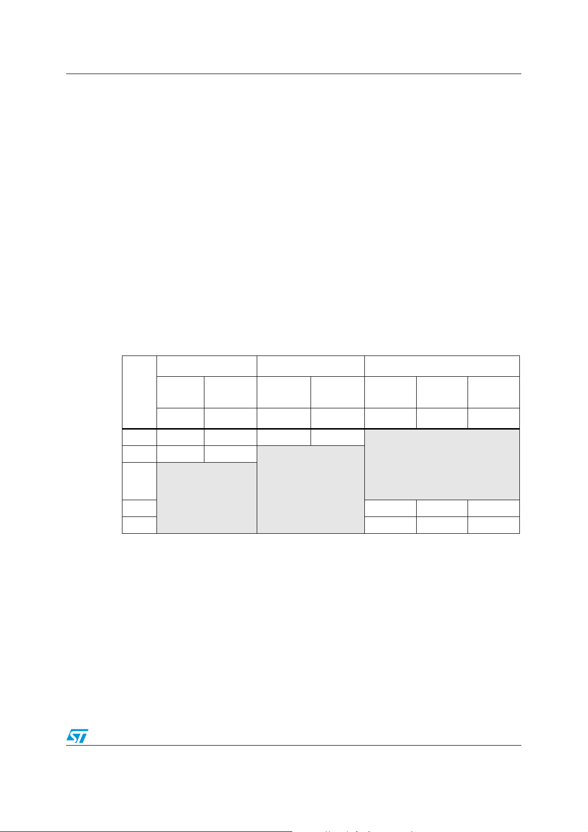
Table 2. STM32F103xx medium-density device features and peripheral counts
Peripheral
Flash - Kbytes 64 128 64 128 64 128 64 128
SRAM - Kbytes 20 20 20 20
General-purpose 33 3 3
Advanced-control 11 1 1
Timers
SPI 12 2 2
2
I
C 12 2 2
USART 23 3 3
USB 11 1 1
Communication
CAN 11 1 1
GPIOs 26 37 51 80
STM32F103Tx STM32F103Cx STM32F103Rx
STM32F103Vx
12-bit synchronized ADC
Number of channels
CPU frequency 72 MHz
Operating voltage 2.0 to 3.6 V
Operating temperatures
Packages VFQFPN36
2
10 channels
Ambient temperatures: –40 to +85 °C /–40 to +105 °C (see Ta bl e 9 )
Junction temperature: –40 to + 125 °C (see Ta bl e 9 )
2
10 channels
LQFP48,
VFQFPN48
16 channels
2
LQFP64,
TFBGA64
2
16 channels
LQFP100,
LFBGA100
10/99 Doc ID 13587 Rev 13
STM32F103x8, STM32F103xB Description
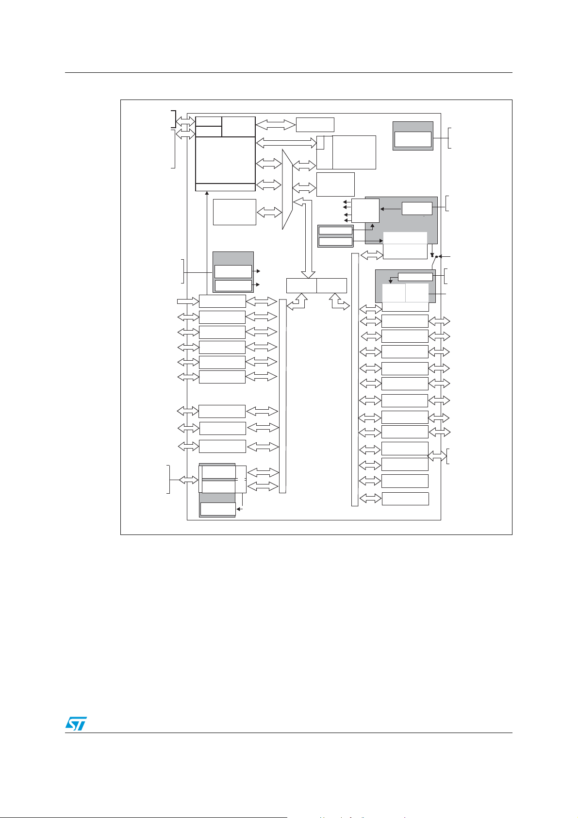
USBDP/CA N_TX
PA[15: 0]
EXTI
WWDG
12bit ADC1
16AF
JTDI
JTCK/ SWCLK
JTMS/SWDIO
NJTRSTTRST
JTDO
NRST
V
DD
= 2 to 3.6V
80AF
PB[15: 0]
PC[15:0 ]
AHB2
MOSI,MISO,SCK,NSS
SRAM
2x(8x16bit)
WAKEUP
GPIOA
GPIOB
GPIOC
F
max
: 72 M
Hz
V
SS
SCL,SDA
I2C2
V
REF+
GP DMA
TIM2
TIM3
XTAL OSC
4-16 MHz
XTAL 32 kHz
OSC_IN
OSC_OUT
OSC32_OUT
OSC32_IN
PLL &
APB1 : F
max
=24 / 36 MHz
PCLK1
HCLK
CLOCK
MANA GT
PCLK2
as AF
as AF
Flash 128 KB
VOLT. REG.
3.3V TO 1.8V
POWER
Backu p i nterf ace
as AF
TIM 4
BusM atrix
64 bit
Interface
20 KB
RTC
RC 8 MHz
Cortex-M3 CPU
Ibus
Dbus
pbu s
obl
flash
SRAM 512B
Trace
Cont roller
USART1
USART2
SPI2
bxCAN
7 channels
Back up
reg
4 Chann els
TIM1
3 com pl. Chann els
SCL,SDA ,SMBA
I2C1
as AF
RX,TX, CTS, RTS,
USART3
Temp sens or
V
REF-
PD[15: 0]
GPIOD
PE[15: 0]
GPIOE
AHB:F
max
=48/72 MHz
ETR and BKIN
4 Chann els
4 Chann els
4 Chann els
FCLK
RC 40 kHz
Stand by
IWDG
@VBAT
POR / PDR
SUPPLY
@VDDA
VDDA
VSSA
@VDDA
V
BAT
RX,TX, CTS, RTS,
Smart Card as AF
RX,TX, CTS, RTS,
CK, SmartCard as AF
APB2 : F
max
=48 / 72 MHz
NVIC
SPI1
MOSI,MISO,
SCK,NSS as AF
12bit ADC2
IF
IFIF
int erface
@VDDA
SUPERVISION
PVD
Rst
Int
@VDD
AHB2
APB2
APB 1
AWU
TAMPER-RTC
@VDD
USB 2.0 FS
USBDM/CAN_RX
System
ai14390d
TRACECLK
TRACED[0:3]
as AS
SW/JTAG
TPIU
Trace/trig
CK, SmartCard as AF
Figure 1. STM32F103xx performance line block diagram
1. TA = –40 °C to +105 °C (junction temperature up to 125 °C).
2. AF = alternate function on I/O port pin.
Doc ID 13587 Rev 13 11/99
Description STM32F103x8, STM32F103xB
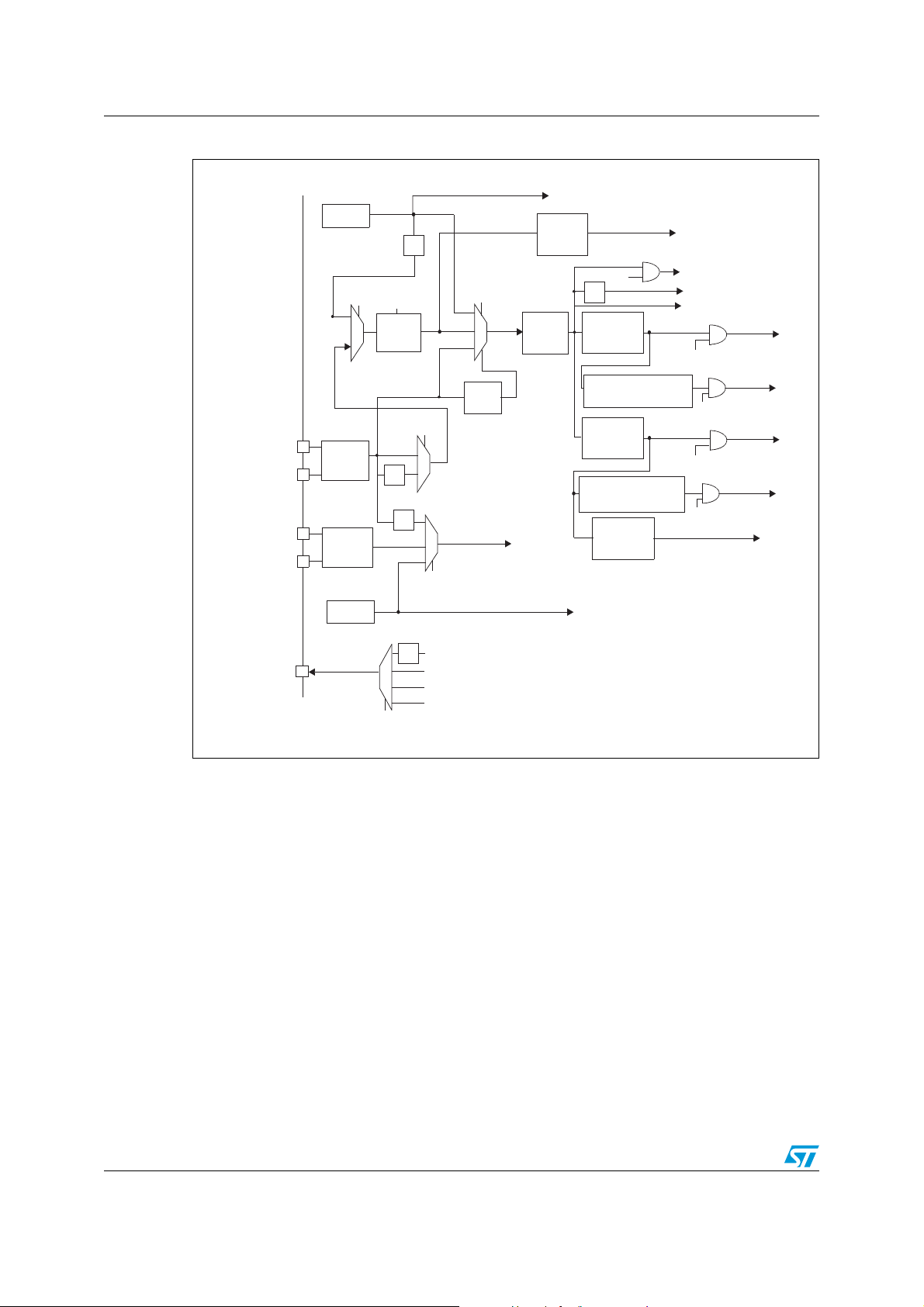
HSE OSC
4-16 MHz
OSC_IN
OSC_OUT
OSC32_IN
OSC32_OUT
LSE OSC
32.768 kHz
HSI RC
8 MHz
LSI RC
40 kHz
to Independent Watchdog (IWDG)
PLL
x2, x3, x4
PLLMUL
Legend:
MCO
Clock Output
Main
PLLXTPRE
/2
..., x16
AHB
Prescaler
/1, 2..512
/2
PLLCLK
HSI
HSE
APB1
Prescaler
/1, 2, 4, 8, 16
ADC
Prescaler
/2, 4, 6, 8
ADCCLK
PCLK1
HCLK
PLLCLK
to AHB bus, core,
memory and DMA
USBCLK
to USB interface
to TIM2, 3
and 4
USB
Prescaler
/1, 1.5
to ADC
LSE
LSI
HSI
/128
/2
HSI
HSE
peripherals
to APB1
Peripheral Clock
Enable (13 bits)
Enable (3 bits)
P
eripheral Clock
APB2
Prescaler
/1, 2, 4, 8, 16
PCLK2
to TIM1
peripherals
to APB2
Peripheral Clock
Enable (11 bits)
Enable (1 bit)
Peripheral Clock
48 MHz
72 MHz max
72 MHz
72 MHz max
36 MHz max
to RTC
PLLSRC
SW
MCO
CSS
to Cortex System timer
/8
Clock
Enable (3 bits)
SYSCLK
max
RTCCLK
RTCSEL[1:0]
TIM1CLK
TIMXCLK
IWDGCLK
SYSCLK
FCLK Cortex
free running clock
TIM2,3, 4
If (APB1 prescaler =1) x1
else x2
TIM1 timer
If (APB2 prescaler =1) x1
else x2
HSE = high-speed external clock signal
HSI = high-speed internal clock signal
LSI = low-speed internal clock signal
LSE = low-speed external clock signal
ai14903
FLITFCLK
to Flash programming interface
Figure 2. Clock tree
1. When the HSI is used as a PLL clock input, the maximum system clock frequency that can be achieved is
64 MHz.
2. For the USB function to be available, both HSE and PLL must be enabled, with USBCLK running at 48
MHz.
3. To have an ADC conversion time of 1 µs, APB2 must be at 14 MHz, 28 MHz or 56 MHz.
12/99 Doc ID 13587 Rev 13
STM32F103x8, STM32F103xB Description
2.2 Full compatibility throughout the family
The STM32F103xx is a complete family whose members are fully pin-to-pin, software and
feature compatible. In the reference manual, the STM32F103x4 and STM32F103x6 are
identified as low-density devices, the STM32F103x8 and STM32F103xB are referred to as
medium-density devices, and the STM32F103xC, STM32F103xD and STM32F103xE are
referred to as high-density devices.
Low- and high-density devices are an extension of the STM32F103x8/B devices, they are
specified in the STM32F103x4/6 and STM32F103xC/D/E datasheets, respectively. Lowdensity devices feature lower Flash memory and RAM capacities, less timers and
peripherals. High-density devices have higher Flash memory and RAM capacities, and
additional peripherals like SDIO, FSMC, I
the other members of the STM32F103xx family.
The STM32F103x4, STM32F103x6, STM32F103xC, STM32F103xD and STM32F103xE
are a drop-in replacement for STM32F103x8/B medium-density devices, allowing the user
to try different memory densities and providing a greater degree of freedom during the
development cycle.
Moreover, the STM32F103xx performance line family is fully compatible with all existing
STM32F101xx access line and STM32F102xx USB access line devices.
Table 3. STM32F103xx family
2
S and DAC, while remaining fully compatible with
Low-density devices Medium-density devices High-density devices
Pinout
144
100
64
48
36
1. For orderable part numbers that do not show the A internal code after the temperature range code (6 or 7),
the reference datasheet for electrical characteristics is that of the STM32F103x8/B medium-density
devices.
16 KB
Flash
6 KB RAM 10 KB RAM 20 KB RAM 20 KB RAM 48 KB RAM 64 KB RAM 64 KB RAM
2 × USARTs
2 × 16-bit timers
1 × SPI, 1 × I
CAN, 1 × PWM timer
2 × ADCs
32 KB
Flash
2
C, USB,
(1)
64 KB
Flash
3 × USARTs
3 × 16-bit timers
2 × SPIs, 2 × I
CAN, 1 × PWM timer
2 × ADCs
128 KB
Flash
2
Cs, USB,
256 KB
Flash
5 × USARTs
4 × 16-bit timers, 2 × basic timers
3 × SPIs, 2 × I
USB, CAN, 2 × PWM timers
3 × ADCs, 2 × DACs, 1 × SDIO
FSMC (100 and 144 pins)
384 KB
Flash
2
Ss, 2 × I2Cs
512 KB
Flash
Doc ID 13587 Rev 13 13/99

Description STM32F103x8, STM32F103xB
2.3 Overview
2.3.1 ARM® Cortex™-M3 core with embedded Flash and SRAM
The ARM Cortex™-M3 processor is the latest generation of ARM processors for embedded
systems. It has been developed to provide a low-cost platform that meets the needs of MCU
implementation, with a reduced pin count and low-power consumption, while delivering
outstanding computational performance and an advanced system response to interrupts.
The ARM Cortex™-M3 32-bit RISC processor features exceptional code-efficiency,
delivering the high-performance expected from an ARM core in the memory size usually
associated with 8- and 16-bit devices.
The STM32F103xx performance line family having an embedded ARM core, is therefore
compatible with all ARM tools and software.
Figure 1 shows the general block diagram of the device family.
2.3.2 Embedded Flash memory
64 or 128 Kbytes of embedded Flash is available for storing programs and data.
2.3.3 CRC (cyclic redundancy check) calculation unit
The CRC (cyclic redundancy check) calculation unit is used to get a CRC code from a 32-bit
data word and a fixed generator polynomial.
Among other applications, CRC-based techniques are used to verify data transmission or
storage integrity. In the scope of the EN/IEC 60335-1 standard, they offer a means of
verifying the Flash memory integrity. The CRC calculation unit helps compute a signature of
the software during runtime, to be compared with a reference signature generated at linktime and stored at a given memory location.
2.3.4 Embedded SRAM
Twenty Kbytes of embedded SRAM accessed (read/write) at CPU clock speed with 0 wait
states.
2.3.5 Nested vectored interrupt controller (NVIC)
The STM32F103xx performance line embeds a nested vectored interrupt controller able to
handle up to 43 maskable interrupt channels (not including the 16 interrupt lines of
Cortex™-M3) and 16 priority levels.
● Closely coupled NVIC gives low-latency interrupt processing
● Interrupt entry vector table address passed directly to the core
● Closely coupled NVIC core interface
● Allows early processing of interrupts
● Processing of late arriving higher priority interrupts
● Support for tail-chaining
● Processor state automatically saved
● Interrupt entry restored on interrupt exit with no instruction overhead
14/99 Doc ID 13587 Rev 13

STM32F103x8, STM32F103xB Description
This hardware block provides flexible interrupt management features with minimal interrupt
latency.
2.3.6 External interrupt/event controller (EXTI)
The external interrupt/event controller consists of 19 edge detector lines used to generate
interrupt/event requests. Each line can be independently configured to select the trigger
event (rising edge, falling edge, both) and can be masked independently. A pending register
maintains the status of the interrupt requests. The EXTI can detect an external line with a
pulse width shorter than the Internal APB2 clock period. Up to 80 GPIOs can be connected
to the 16 external interrupt lines.
2.3.7 Clocks and startup
System clock selection is performed on startup, however the internal RC 8 MHz oscillator is
selected as default CPU clock on reset. An external 4-16 MHz clock can be selected, in
which case it is monitored for failure. If failure is detected, the system automatically switches
back to the internal RC oscillator. A software interrupt is generated if enabled. Similarly, full
interrupt management of the PLL clock entry is available when necessary (for example on
failure of an indirectly used external crystal, resonator or oscillator).
Several prescalers allow the configuration of the AHB frequency, the high-speed APB
(APB2) and the low-speed APB (APB1) domains. The maximum frequency of the AHB and
the high-speed APB domains is 72 MHz. The maximum allowed frequency of the low-speed
APB domain is 36 MHz. See Figure 2 for details on the clock tree.
2.3.8 Boot modes
At startup, boot pins are used to select one of three boot options:
● Boot from User Flash
● Boot from System Memory
● Boot from embedded SRAM
The boot loader is located in System Memory. It is used to reprogram the Flash memory by
using USART1. For further details please refer to AN2606.
2.3.9 Power supply schemes
● V
● V
● V
For more details on how to connect power pins, refer to Figure 13: Power supply scheme.
= 2.0 to 3.6 V: external power supply for I/Os and the internal regulator.
DD
Provided externally through V
, V
SSA
= 2.0 to 3.6 V: external analog power supplies for ADC, reset blocks, RCs
DDA
and PLL (minimum voltage to be applied to V
V
and V
DDA
= 1.8 to 3.6 V: power supply for RTC, external clock 32 kHz oscillator and backup
BAT
must be connected to V
SSA
registers (through power switch) when V
2.3.10 Power supply supervisor
The device has an integrated power-on reset (POR)/power-down reset (PDR) circuitry. It is
always active, and ensures proper operation starting from/down to 2 V. The device remains
DD
pins.
is 2.4 V when the ADC is used).
DDA
and VSS, respectively.
DD
is not present.
DD
Doc ID 13587 Rev 13 15/99

Description STM32F103x8, STM32F103xB
in reset mode when V
external reset circuit.
The device features an embedded programmable voltage detector (PVD) that monitors the
V
DD/VDDA
generated when V
than the V
power supply and compares it to the V
DD/VDDA
threshold. The interrupt service routine can then generate a warning
PVD
message and/or put the MCU into a safe state. The PVD is enabled by software.
Refer to Table 11: Embedded reset and power control block characteristics for the values of
V
POR/PDR
and V
PVD
.
2.3.11 Voltage regulator
The regulator has three operation modes: main (MR), low power (LPR) and power down.
● MR is used in the nominal regulation mode (Run)
● LPR is used in the Stop mode
● Power down is used in Standby mode: the regulator output is in high impedance: the
kernel circuitry is powered down, inducing zero consumption (but the contents of the
registers and SRAM are lost)
This regulator is always enabled after reset. It is disabled in Standby mode, providing high
impedance output.
2.3.12 Low-power modes
is below a specified threshold, V
DD
drops below the V
PVD
threshold and/or when VDD/V
PVD
POR/PDR
, without the need for an
threshold. An interrupt can be
is higher
DDA
The STM32F103xx performance line supports three low-power modes to achieve the best
compromise between low power consumption, short startup time and available wakeup
sources:
● Sleep mode
In Sleep mode, only the CPU is stopped. All peripherals continue to operate and can
wake up the CPU when an interrupt/event occurs.
● Stop mode
The Stop mode achieves the lowest power consumption while retaining the content of
SRAM and registers. All clocks in the 1.8 V domain are stopped, the PLL, the HSI RC
and the HSE crystal oscillators are disabled. The voltage regulator can also be put
either in normal or in low power mode.
The device can be woken up from Stop mode by any of the EXTI line. The EXTI line
source can be one of the 16 external lines, the PVD output, the RTC alarm or the USB
wakeup.
● Standby mode
The Standby mode is used to achieve the lowest power consumption. The internal
voltage regulator is switched off so that the entire 1.8 V domain is powered off. The
PLL, the HSI RC and the HSE crystal oscillators are also switched off. After entering
Standby mode, SRAM and register contents are lost except for registers in the Backup
domain and Standby circuitry.
The device exits Standby mode when an external reset (NRST pin), an IWDG reset, a
rising edge on the WKUP pin, or an RTC alarm occurs.
Note: The RTC, the IWDG, and the corresponding clock sources are not stopped by entering Stop
or Standby mode.
16/99 Doc ID 13587 Rev 13
STM32F103x8, STM32F103xB Description
2.3.13 DMA
The flexible 7-channel general-purpose DMA is able to manage memory-to-memory,
peripheral-to-memory and memory-to-peripheral transfers. The DMA controller supports
circular buffer management avoiding the generation of interrupts when the controller
reaches the end of the buffer.
Each channel is connected to dedicated hardware DMA requests, with support for software
trigger on each channel. Configuration is made by software and transfer sizes between
source and destination are independent.
The DMA can be used with the main peripherals: SPI, I
2
C, USART, general-purpose and
advanced-control timers TIMx and ADC.
2.3.14 RTC (real-time clock) and backup registers
The RTC and the backup registers are supplied through a switch that takes power either on
V
supply when present or through the V
DD
registers used to store 20 bytes of user application data when V
The real-time clock provides a set of continuously running counters which can be used with
suitable software to provide a clock calendar function, and provides an alarm interrupt and a
periodic interrupt. It is clocked by a 32.768 kHz external crystal, resonator or oscillator, the
internal low-power RC oscillator or the high-speed external clock divided by 128. The
internal low-power RC has a typical frequency of 40 kHz. The RTC can be calibrated using
an external 512 Hz output to compensate for any natural crystal deviation. The RTC features
a 32-bit programmable counter for long-term measurement using the Compare register to
generate an alarm. A 20-bit prescaler is used for the time base clock and is by default
configured to generate a time base of 1 second from a clock at 32.768 kHz.
pin. The backup registers are ten 16-bit
BAT
power is not present.
DD
2.3.15 Timers and watchdogs
The medium-density STM32F103xx performance line devices include an advanced-control
timer, three general-purpose timers, two watchdog timers and a SysTick timer.
Ta bl e 4 compares the features of the advanced-control and general-purpose timers.
Table 4. Timer feature comparison
Timer
TIM1 16-bit
TIM2,
TIM3,
TIM4
Counter
resolution
16-bit
Counter
type
Up,
down,
up/down
Up,
down,
up/down
Prescaler
factor
Any integer
between 1
and 65536
Any integer
between 1
and 65536
DMA request
generation
Ye s 4 Ye s
Ye s 4 N o
Capture/compare
channels
Complementary
outputs
Doc ID 13587 Rev 13 17/99

Description STM32F103x8, STM32F103xB
Advanced-control timer (TIM1)
The advanced-control timer (TIM1) can be seen as a three-phase PWM multiplexed on 6
channels. It has complementary PWM outputs with programmable inserted dead-times. It
can also be seen as a complete general-purpose timer. The 4 independent channels can be
used for
● Input capture
● Output compare
● PWM generation (edge- or center-aligned modes)
● One-pulse mode output
If configured as a general-purpose 16-bit timer, it has the same features as the TIMx timer. If
configured as the 16-bit PWM generator, it has full modulation capability (0-100%).
In debug mode, the advanced-control timer counter can be frozen and the PWM outputs
disabled to turn off any power switch driven by these outputs.
Many features are shared with those of the general-purpose TIM timers which have the
same architecture. The advanced-control timer can therefore work together with the TIM
timers via the Timer Link feature for synchronization or event chaining.
General-purpose timers (TIMx)
There are up to three synchronizable general-purpose timers embedded in the
STM32F103xx performance line devices. These timers are based on a 16-bit auto-reload
up/down counter, a 16-bit prescaler and feature 4 independent channels each for input
capture/output compare, PWM or one-pulse mode output. This gives up to 12 input
captures/output compares/PWMs on the largest packages.
The general-purpose timers can work together with the advanced-control timer via the Timer
Link feature for synchronization or event chaining. Their counter can be frozen in debug
mode. Any of the general-purpose timers can be used to generate PWM outputs. They all
have independent DMA request generation.
These timers are capable of handling quadrature (incremental) encoder signals and the
digital outputs from 1 to 3 hall-effect sensors.
Independent watchdog
The independent watchdog is based on a 12-bit downcounter and 8-bit prescaler. It is
clocked from an independent 40 kHz internal RC and as it operates independently of the
main clock, it can operate in Stop and Standby modes. It can be used either as a watchdog
to reset the device when a problem occurs, or as a free-running timer for application timeout
management. It is hardware- or software-configurable through the option bytes. The counter
can be frozen in debug mode.
Window watchdog
The window watchdog is based on a 7-bit downcounter that can be set as free-running. It
can be used as a watchdog to reset the device when a problem occurs. It is clocked from the
main clock. It has an early warning interrupt capability and the counter can be frozen in
debug mode.
18/99 Doc ID 13587 Rev 13

STM32F103x8, STM32F103xB Description
SysTick timer
This timer is dedicated for OS, but could also be used as a standard downcounter. It
features:
● A 24-bit downcounter
● Autoreload capability
● Maskable system interrupt generation when the counter reaches 0
● Programmable clock source
2.3.16 I²C bus
Up to two I²C bus interfaces can operate in multimaster and slave modes. They can support
standard and fast modes.
They support dual slave addressing (7-bit only) and both 7/10-bit addressing in master
mode. A hardware CRC generation/verification is embedded.
They can be served by DMA and they support SM Bus 2.0/PM Bus.
2.3.17 Universal synchronous/asynchronous receiver transmitter (USART)
One of the USART interfaces is able to communicate at speeds of up to 4.5 Mbit/s. The
other available interfaces communicate at up to 2.25 Mbit/s. They provide hardware
management of the CTS and RTS signals, IrDA SIR ENDEC support, are ISO 7816
compliant and have LIN Master/Slave capability.
All USART interfaces can be served by the DMA controller.
2.3.18 Serial peripheral interface (SPI)
Up to two SPIs are able to communicate up to 18 Mbits/s in slave and master modes in fullduplex and simplex communication modes. The 3-bit prescaler gives 8 master mode
frequencies and the frame is configurable to 8 bits or 16 bits. The hardware CRC
generation/verification supports basic SD Card/MMC modes.
Both SPIs can be served by the DMA controller.
2.3.19 Controller area network (CAN)
The CAN is compliant with specifications 2.0A and B (active) with a bit rate up to 1 Mbit/s. It
can receive and transmit standard frames with 11-bit identifiers as well as extended frames
with 29-bit identifiers. It has three transmit mailboxes, two receive FIFOs with 3 stages and
14 scalable filter banks.
2.3.20 Universal serial bus (USB)
The STM32F103xx performance line embeds a USB device peripheral compatible with the
USB full-speed 12 Mbs. The USB interface implements a full-speed (12 Mbit/s) function
interface. It has software-configurable endpoint setting and suspend/resume support. The
dedicated 48 MHz clock is generated from the internal main PLL (the clock source must use
a HSE crystal oscillator).
Doc ID 13587 Rev 13 19/99

Description STM32F103x8, STM32F103xB
2.3.21 GPIOs (general-purpose inputs/outputs)
Each of the GPIO pins can be configured by software as output (push-pull or open-drain), as
input (with or without pull-up or pull-down) or as peripheral alternate function. Most of the
GPIO pins are shared with digital or analog alternate functions. All GPIOs are high-currentcapable except for analog inputs.
The I/Os alternate function configuration can be locked if needed following a specific
sequence in order to avoid spurious writing to the I/Os registers.
I/Os on APB2 with up to 18 MHz toggling speed
2.3.22 ADC (analog-to-digital converter)
Two 12-bit analog-to-digital converters are embedded into STM32F103xx performance line
devices and each ADC shares up to 16 external channels, performing conversions in singleshot or scan modes. In scan mode, automatic conversion is performed on a selected group
of analog inputs.
Additional logic functions embedded in the ADC interface allow:
● Simultaneous sample and hold
● Interleaved sample and hold
● Single shunt
The ADC can be served by the DMA controller.
An analog watchdog feature allows very precise monitoring of the converted voltage of one,
some or all selected channels. An interrupt is generated when the converted voltage is
outside the programmed thresholds.
The events generated by the general-purpose timers (TIMx) and the advanced-control timer
(TIM1) can be internally connected to the ADC start trigger, injection trigger, and DMA
trigger respectively, to allow the application to synchronize A/D conversion and timers.
2.3.23 Temperature sensor
The temperature sensor has to generate a voltage that varies linearly with temperature. The
conversion range is between 2 V < V
< 3.6 V. The temperature sensor is internally
DDA
connected to the ADC12_IN16 input channel which is used to convert the sensor output
voltage into a digital value.
2.3.24 Serial wire JTAG debug port (SWJ-DP)
The ARM SWJ-DP Interface is embedded. and is a combined JTAG and serial wire debug
port that enables either a serial wire debug or a JTAG probe to be connected to the target.
The JTAG TMS and TCK pins are shared with SWDIO and SWCLK, respectively, and a
specific sequence on the TMS pin is used to switch between JTAG-DP and SW-DP.
20/99 Doc ID 13587 Rev 13

STM32F103x8, STM32F103xB Pinouts and pin description
AI16001c
PE10
PC14-
OSC32_IN
PC5PA5
PC3
PB4
PE15
PB2
PC4PA4
H
PE14
PE11PE7
D PD4
PD3
PB8PE3
C
PD0
PC12
PE5
PB5
PC0
PE2
B PC11PD2
PC15-
OSC32_OUT
PB7
PB6
A
87654321
V
SS_5
OSC_IN
OSC_OUT V
DD_5
G
F
E
PC1
V
REF–
PC13-
TAMPER-RTC
PB9
PA15
PB3
PE4
PE1
PE0
V
SS_1
PD1PE6NRST
PC2
V
SS_3
V
SS_4
NCV
DD_3
V
DD_4
PB15
V
BAT
PD5
PD6
BOOT0 PD7
V
SS_2
V
SSA
PA1
V
DD_2
V
DD_1
PB14
PA0-WKUP
109
K
J
PD10
PD11
PA8
PA9
PA10
PA11
PA12
PC10
PA13
PA14
PC9
PC7
PC6
PD15
PC8
PD14
PE12
PB1PA7
PB11
PE8
PB0PA6
PB10
PE13PE9V
DDA
PB13
V
REF+
PA3
PB12
PA2
PD8
PD9 PD13
PD12
3 Pinouts and pin description
Figure 3. STM32F103xx performance line LFBGA100 ballout
Doc ID 13587 Rev 13 21/99
Pinouts and pin description STM32F103x8, STM32F103xB
100999897969594939291908988878685848382818079787776
1
2
3
4
5
6
7
8
9
10
11
12
13
14
15
16
17
18
19
20
21
22
23
24
25
75
74
73
72
71
70
69
68
67
66
65
64
63
62
61
60
59
58
57
56
55
54
53
52
51
VDD_2
VSS_2
NC
PA 1 3
PA 1 2
PA 1 1
PA 1 0
PA 9
PA 8
PC9
PC8
PC7
PC6
PD15
PD14
PD13
PD12
PD11
PD10
PD9
PD8
PB15
PB14
PB13
PB12
PA 3
VSS_4
VDD_4
PA 4
PA 5
PA 6
PA 7
PC4
PC5
PB0
PB1
PB2
PE7
PE8
PE9
PE10
PE11
PE12
PE13
PE14
PE15
PB10
PB11
VSS_1
VDD_1
VDD_3
VSS_3
PE1
PE0
PB9
PB8
BOOT0
PB7
PB6
PB5
PB4
PB3
PD7
PD6
PD5
PD4
PD3
PD2
PD1
PD0
PC12
PC11
PC10
PA15
PA14
26272829303132333435363738394041424344454647484950
PE2
PE3
PE4
PE5
PE6
VBAT
PC13-TAMPER-RTC
PC14-OSC32_IN
PC15-OSC32_OUT
VSS_5
VDD_5
OSC_IN
OSC_OUT
NRST
PC0
PC1
PC2
PC3
VSSA
VREF-
VREF+
VDDA
PA 0- W K UP
PA 1
PA 2
ai14391
LQFP100
Figure 4. STM32F103xx performance line LQFP100 pinout
22/99 Doc ID 13587 Rev 13

STM32F103x8, STM32F103xB Pinouts and pin description
64 63 62 61 60 59 58 57 56 55 54 53 52 51 50 49
48
47
46
45
44
43
42
41
40
39
38
37
36
35
34
33
17 18 19 20 21 22 23 24 29 30 31 3225 26 27 28
1
2
3
4
5
6
7
8
9
10
11
12
13
14
15
16
VBAT
PC13-TAMPER-RTC
PC14-OSC32_IN
PC15-OSC32_OUT
PD0 OSC_IN
PD1 OSC_OUT
NRST
PC0
PC1
PC2
PC3
VSSA
VDDA
PA 0- W K UP
PA 1
PA 2
VDD_3
VSS_3
PB9
PB8
BOOT0
PB7
PB6
PB5
PB4
PB3
PD2
PC12
PC11
PC10
PA 1 5
PA 14
VDD_2
VSS_2
PA 1 3
PA 1 2
PA 1 1
PA 1 0
PA 9
PA 8
PC9
PC8
PC7
PC6
PB15
PB14
PB13
PB12
PA 3
VSS_4
VDD_4
PA 4
PA 5
PA 6
PA 7
PC4
PC5
PB0
PB1
PB2
PB10
PB11
VSS_1
VDD_1
LQFP64
ai14392
Figure 5. STM32F103xx performance line LQFP64 pinout
Doc ID 13587 Rev 13 23/99
Pinouts and pin description STM32F103x8, STM32F103xB
AI15494
PB2
PC14-
OSC32_IN
PA7PA4
PA2
PA15
PB11
PB1PA6PA3
H
PB10
PC5PC4
D PA8
PA9
BOOT0PB8
C
PC9
PA11
PB6
PC12
V
DDA
PB9
B
PA12
PC10
PC15-
OSC32_OUT
PB3
PD2
A
87654321
V
SS_4
OSC_IN
OSC_OUT V
DD_4
G
F
E
PC2
V
REF+
PC13-
TAMPER-RTC
PB4 PA13PA14
PB7
PB5
V
SS_3
PC7 PC8PC0NRST PC1
PB0PA5 PB14
V
DD_2
V
DD_3
PB13
V
BAT
PC11
PA10
V
SS_2
V
SS_1
PC6V
SSA
PA1
V
DD_1
PB15
PB12
PA0-WKUP
Figure 6. STM32F103xx performance line TFBGA64 ballout
24/99 Doc ID 13587 Rev 13
STM32F103x8, STM32F103xB Pinouts and pin description
ai18300
VDD_3
VSS_3
PB9
PB8
BOOT0
PB7
PB6
PB5
PB4
PB3
PA15
PA14
PA 3
PA 4
PA 5
PA 6
PA 7
PB0
PB1
PB2
PB10
PB11
VSS_1
VDD_1
VBAT
PC13-TAMPER-RTC
PC14-OSC32_IN
PC15-OSC32_OUT
PD0-OSC_IN
PD1-OSC_OUT
NRST
VSSA
VDDA
PA0-WKUP
PA 1
PA 2
VDD_2
VSS_2
PA13
PA12
PA11
PA10
PA 9
PA 8
PB15
PB14
PB13
PB12
48
VFQFPN48
47 46
45 444342 41
40 39 38 37
36
35
34
33
32
31
30
29
28
27
26
25
13
14 15
16 171819 20
21 22 23 24
1
2
3
4
5
6
7
8
9
10
11
12
Figure 7. STM32F103xx performance line LQFP48 pinout
VDD_3
VSS_3
PB9
PB8
BOOT0
PB7
PB6
PB5
PB4
PB3
PA1 5
PA 14
PC13-TAMPER-RTC
VBAT
PC14-OSC32_IN
PC15-OSC32_OUT
PD0-OSC_IN
PD1-OSC_OUT
NRST
VSSA
VDDA
PA 0- W K UP
PA 1
PA 2
48 47 46 45
1
2
3
4
5
6
7
8
9
10
11
12
13 14 15 16 17 18 19 20 21 22
PA 3
44 43 42 41 40 39 38 37
LQFP48
PA 4
PA 5
PA 6
PA 7
PB0
PB1
PB2
VDD_2
36
VSS_2
35
PA1 3
34
PA1 2
33
PA1 1
32
PA1 0
31
PA9
30
PA8
29
PB15
28
27
PB14
26
PB13
25
PB12
24
23
PB10
PB11
VSS_1
VDD_1
ai14393b
Figure 8. STM32F103xx performance line VFQFPN48 pinout
Doc ID 13587 Rev 13 25/99
Pinouts and pin description STM32F103x8, STM32F103xB
V
SS_3
BOOT0
PB7
PB6
PB5
PB4
PB3
PA15
PA14
36 35 34 33 32 31 30 29 28
V
DD_3
1
27
V
DD_2
OSC_IN/PD0
2
26
V
SS_2
OSC_OUT/PD1
3
25
PA13
NRST
4
QFN36
24
PA12
V
SSA
5
23 PA11
V
DDA
6
22
PA10
PA0-WKUP
7
21
PA 9
PA 1
8
20
PA 8
PA 2 9
19
V
DD_1
10 11 12 13 14 15 16 17 18
PA 3
PA 4
PA 5
PA 6
PA 7
PB0
PB1
PB2
V
SS_1
ai14654
Figure 9. STM32F103xx performance line VFQFPN36 pinout
26/99 Doc ID 13587 Rev 13
STM32F103x8, STM32F103xB Pinouts and pin description
Table 5. Medium-density STM32F103xx pin definitions
LFBGA100
Pins
LQFP64
TFBGA64
LQFP100
Pin name
VFQFPN36
(1)
Type
(2)
Main
function
(after reset)
I / O Level
(3)
Alternate functions
Default Remap
LQFP48/VFQFPN48
A3 - - 1 - PE2 I/O FT PE2 TRACECK
B3 - - 2 - PE3 I/O FT PE3 TRACED0
C3 - - 3 - PE4 I/O FT PE4 TRACED1
D3 - - 4 - PE5 I/O FT PE5 TRACED2
E3 - - 5 - PE6 I/O FT PE6 TRACED3
B2 1 B2 1 6 - V
A2 2 A2 2 7 -
BAT
PC13-TAMPER-
RTC
(5)
A1 3 A1 3 8 - PC14-OSC32_IN
B1 4 B1 4 9 -
C2---10- V
D2---11- V
PC15-
OSC32_OUT
SS_5
DD_5
SV
I/O PC13
(5)
I/O PC14
I/O PC15
(5)
SV
SV
BAT
SS_5
DD_5
(6)
(6)
(6)
TAMPER-RTC
OSC32_IN
OSC32_OUT
C1 5 C1 5 12 2 OSC_IN I OSC_IN
D1 6 D1 6 13 3 OSC_OUT O OSC_OUT
E1 7 E1 7 14 4 NRST I/O NRST
F1 - E3 8 15 - PC0 I/O PC0 ADC12_IN10
F2 - E2 9 16 - PC1 I/O PC1 ADC12_IN11
E2 - F2 10 17 - PC2 I/O PC2 ADC12_IN12
F3 - -
G1 8 F1 12 19 5 V
H1---20- V
J1 - G1
K1 9 H1 13 22 6 V
(7)
11 18 - PC3 I/O PC3 ADC12_IN13
SV
SV
SV
SV
SSA
REF-
REF+
DDA
(7)
-21- V
SSA
REF-
REF+
DDA
WKUP/
G2 10 G2 14 23 7 PA0-WKUP I/O PA0
USART2_CTS
ADC12_IN0/
TIM2_CH1_ETR
USART2_RTS
H2 11 H2 15 24 8 PA1 I/O PA1
ADC12_IN1/
TIM2_CH2
(8)
(8)
(8)
(4)
/
(8)
/
Doc ID 13587 Rev 13 27/99
Pinouts and pin description STM32F103x8, STM32F103xB
Table 5. Medium-density STM32F103xx pin definitions (continued)
(4)
LFBGA100
Pins
TFBGA64
Alternate functions
(2)
Pin name
(1)
Type
LQFP64
LQFP100
VFQFPN36
Main
function
(after reset)
I / O Level
(3)
Default Remap
LQFP48/VFQFPN48
(8)
(8)
(8)
(8)
(8)
(8)
/
/
/
/
J2 12 F3 16 25 9 PA2 I/O PA2
K2 13 G3 17 26 10 PA3 I/O PA3
E4 - C2 18 27 - V
F4 - D2 19 28 - V
SS_4
DD_4
SV
SV
SS_4
DD_4
G3 14 H3 20 29 11 PA4 I/O PA4
USART2_TX
ADC12_IN2/
TIM2_CH3
USART2_RX
ADC12_IN3/
TIM2_CH4
SPI1_NSS
USART2_CK
ADC12_IN4
H3 15 F4 21 30 12 PA5 I/O PA5
J3 16 G4 22 31 13 PA6 I/O PA6
K3 17 H4 23 32 14 PA7 I/O PA7
SPI1_SCK
ADC12_IN5
SPI1_MISO
ADC12_IN6/
TIM3_CH1
SPI1_MOSI
ADC12_IN7/
TIM3_CH2
(8)
(8)
(8)
(8)
(8)
/
/
TIM1_BKIN
/
TIM1_CH1N
G4 - H5 24 33 PC4 I/O PC4 ADC12_IN14
H4 - H6 25 34 PC5 I/O PC5 ADC12_IN15
J4 18 F5 26 35 15 PB0 I/O PB0
K4 19 G5 27 36 16 PB1 I/O PB1
ADC12_IN8/
TIM3_CH3
ADC12_IN9/
TIM3_CH4
(8)
(8)
TIM1_CH2N
TIM1_CH3N
G5 20 G6 28 37 17 PB2 I/O FT PB2/BOOT1
H5 - - - 38 - PE7 I/O FT PE7 TIM1_ETR
J5 - - - 39 - PE8 I/O FT PE8 TIM1_CH1N
K5 - - - 40 - PE9 I/O FT PE9 TIM1_CH1
G6 - - - 41 - PE10 I/O FT PE10 TIM1_CH2N
H6 - - - 42 - PE11 I/O FT PE11 TIM1_CH2
J6 - - - 43 - PE12 I/O FT PE12 TIM1_CH3N
K6 - - - 44 - PE13 I/O FT PE13 TIM1_CH3
G7 - - - 45 - PE14 I/O FT PE14 TIM1_CH4
28/99 Doc ID 13587 Rev 13
STM32F103x8, STM32F103xB Pinouts and pin description
Table 5. Medium-density STM32F103xx pin definitions (continued)
(4)
TIM2_CH3
TIM2_CH4
TIM4_CH1 /
USART3_RTS
LFBGA100
Pins
TFBGA64
(2)
Pin name
(1)
Type
LQFP64
LQFP100
VFQFPN36
Main
function
(after reset)
I / O Level
(3)
Alternate functions
Default Remap
LQFP48/VFQFPN48
H7 - - - 46 - PE15 I/O FT PE15 TIM1_BKIN
J7 21 G7 29 47 - PB10 I/O FT PB10
K7 22 H7 30 48 - PB11 I/O FT PB11
E7 23 D6 31 49 18 V
F7 24 E6 32 50 19 V
SS_1
DD_1
SV
SV
SS_1
DD_1
I2C2_SCL/
USART3_TX
I2C2_SDA/
USART3_RX
(8)
(8)
SPI2_NSS/
K8 25 H8 33 51 - PB12 I/O FT PB12
J8 26 G8 34 52 - PB13 I/O FT PB13
H8 27 F8 35 53 - PB14 I/O FT PB14
G8 28 F7 36 54 - PB15 I/O FT PB15
I2C2_SMBAl/
USART3_CK
TIM1_BKIN
SPI2_SCK/
USART3_CTS
TIM1_CH1N
SPI2_MISO/
USART3_RTS
TIM1_CH2N
SPI2_MOSI/
TIM1_CH3N
(8)
(8)
(8)
(8)
(8)
(8)
(8)
/
/
K9 - - - 55 - PD8 I/O FT PD8 USART3_TX
J9 - - - 56 - PD9 I/O FT PD9 USART3_RX
H9 - - - 57 - PD10 I/O FT PD10 USART3_CK
G9 - - - 58 - PD11 I/O FT PD11 USART3_CTS
K10 - - - 59 - PD12 I/O FT PD12
J10 - - - 60 - PD13 I/O FT PD13 TIM4_CH2
H10 - - - 61 - PD14 I/O FT PD14 TIM4_CH3
G10 - - - 62 - PD15 I/O FT PD15 TIM4_CH4
F10 - F6 37 63 - PC6 I/O FT PC6 TIM3_CH1
E10 E7 38 64 - PC7 I/O FT PC7 TIM3_CH2
F9 E8 39 65 - PC8 I/O FT PC8 TIM3_CH3
E9 - D8 40 66 - PC9 I/O FT PC9 TIM3_CH4
D9 29 D7 41 67 20 PA8 I/O FT PA8
USART1_CK/
TIM1_CH1
(8)
/MCO
Doc ID 13587 Rev 13 29/99
Pinouts and pin description STM32F103x8, STM32F103xB
Table 5. Medium-density STM32F103xx pin definitions (continued)
(4)
LFBGA100
Pins
TFBGA64
Alternate functions
(2)
Pin name
(1)
Type
LQFP64
LQFP100
VFQFPN36
Main
function
(after reset)
I / O Level
(3)
Default Remap
LQFP48/VFQFPN48
(8)
C9 30 C7 42 68 21 PA9 I/O FT PA9
D1031C6436922 PA10 I/OFT PA10
C1032C8447023 PA11 I/OFT PA11
B1033B8457124 PA12 I/OFT PA12
USART1_TX
TIM1_CH2
USART1_RX
TIM1_CH3
USART1_CTS/
CANRX
(8)
TIM1_CH4
USART1_RTS/
CANTX
(8)
TIM1_ETR
/
(8)
(8)
/
(8)
/ USBDM
(8)
//USBDP
(8)
A10 34 A8 46 72 25 PA13 I/O FT JTMS/SWDIO PA13
F8 - - - 73 - Not connected
E6 35 D5 47 74 26 V
F6 36 E5 48 75 27 V
SS_2
DD_2
SV
SV
SS_2
DD_2
A9 37 A7 49 76 28 PA14 I/O FT JTCK/SWCLK PA14
A8 38 A6 50 77 29 PA15 I/O FT JTDI
TIM2_CH1_ETR/
PA 1 5 / S P I 1_ N S S
B9 - B7 51 78 PC10 I/O FT PC10 USART3_TX
B8 - B6 52 79 PC11 I/O FT PC11 USART3_RX
C8 - C5 53 80 PC12 I/O FT PC12 USART3_CK
D8 5 C1 5 81 2 PD0 I/O FT OSC_IN
E8 6 D1 6 82 3 PD1 I/O FT OSC_OUT
(9)
(9)
CANRX
CANTX
B7 B5 54 83 - PD2 I/O FT PD2 TIM3_ETR
C7 - - - 84 - PD3 I/O FT PD3 USART2_CTS
D7 - - - 85 - PD4 I/O FT PD4 USART2_RTS
B6 - - - 86 - PD5 I/O FT PD5 USART2_TX
C6 - - - 87 - PD6 I/O FT PD6 USART2_RX
D6 - - - 88 - PD7 I/O FT PD7 USART2_CK
TIM2_CH2 / PB3
A7 39 A5 55 89 30 PB3 I/O FT JTDO
TRACESWO
SPI1_SCK
A6 40 A4 56 90 31 PB4 I/O FT JNTRST
TIM3_CH1/ PB4/
SPI1_MISO
30/99 Doc ID 13587 Rev 13
STM32F103x8, STM32F103xB Pinouts and pin description
Table 5. Medium-density STM32F103xx pin definitions (continued)
(4)
LFBGA100
LQFP48/VFQFPN48
Pins
TFBGA64
Alternate functions
(2)
Pin name
(1)
Type
LQFP64
LQFP100
VFQFPN36
Main
function
(after reset)
I / O Level
(3)
Default Remap
/
/
TIM3_CH2 /
SPI1_MOSI
USART1_TX
USART1_RX
C5 41 C4 57 91 32 PB5 I/O PB5 I2C1_SMBAl
B5 42 D3 58 92 33 PB6 I/O FT PB6
A5 43 C3 59 93 34 PB7 I/O FT PB7
I2C1_SCL
TIM4_CH1
I2C1_SDA
TIM4_CH2
(8)
(8)
(8)
(8)
D5 44 B4 60 94 35 BOOT0 I BOOT0
B4 45 B3 61 95 - PB8 I/O FT PB8 TIM4_CH3
A4 46 A3 62 96 - PB9 I/O FT PB9 TIM4_CH4
(8)
(8)
I2C1_SCL /
CANRX
I2C1_SDA/
CANTX
D4 - - - 97 - PE0 I/O FT PE0 TIM4_ETR
C4 - - - 98 - PE1 I/O FT PE1
E5 47 D4 63 99 36 V
F5 48 E4 64 100 1 V
1. I = input, O = output, S = supply.
2. FT = 5 V tolerant.
3. Function availability depends on the chosen device. For devices having reduced peripheral counts, it is always the lower
number of peripheral that is included. For example, if a device has only one SPI and two USARTs, they will be called SPI1
and USART1 & USART2, respectively. Refer to Table 2 on page 10.
4. If several peripherals share the same I/O pin, to avoid conflict between these alternate functions only one peripheral should
be enabled at a time through the peripheral clock enable bit (in the corresponding RCC peripheral clock enable register).
5. PC13, PC14 and PC15 are supplied through the power switch. Since the switch only sinks a limited amount of current
(3 mA), the use of GPIOs PC13 to PC15 in output mode is limited: the speed should not exceed 2 MHz with a maximum
load of 30 pF and these IOs must not be used as a current source (e.g. to drive an LED).
6. Main function after the first backup domain power-up. Later on, it depends on the contents of the Backup registers even
after reset (because these registers are not reset by the main reset). For details on how to manage these IOs, refer to the
Battery backup domain and BKP register description sections in the STM32F10xxx reference manual, available from the
STMicroelectronics website: www.st.com.
7. Unlike in the LQFP64 package, there is no PC3 in the TFBGA64 package. The V
8. This alternate function can be remapped by software to some other port pins (if available on the used package). For more
details, refer to the Alternate function I/O and debug configuration section in the STM32F10xxx reference manual, available
from the STMicroelectronics website: www.st.com.
9. The pins number 2 and 3 in the VFQFPN36 package, 5 and 6 in the LQFP48 and LQFP64 packages, and C1 and C2 in the
TFBGA64 package are configured as OSC_IN/OSC_OUT after reset, however the functionality of PD0 and PD1 can be
remapped by software on these pins. For the LQFP100 package, PD0 and PD1 are available by default, so there is no
need for remapping. For more details, refer to the Alternate function I/O and debug configuration section in the
STM32F10xxx reference manual.
The use of PD0 and PD1 in output mode is limited as they can only be used at 50 MHz in output mode.
SS_3
DD_3
SV
SV
SS_3
DD_3
REF+
functionality is provided instead.
Doc ID 13587 Rev 13 31/99

Memory mapping STM32F103x8, STM32F103xB
4 Memory mapping
The memory map is shown in Figure 10.
Figure 10. Memory map
APB memory space
0xFFFF FFFF
7
0xE010 0000
0xE000 0000
6
0xC000 0000
5
0xA000 0000
4
0x8000 0000
3
0x6000 0000
2
0x4000 0000
1
0x2000 0000
0
0x0000 0000
Cortex- M3 Internal
Perip heral s
Peripherals
SRAM
Reserved
0x1FFF FFFF
0x1FFF F80F
0x1FFF F800
0x1FFF F000
0x0801 FFFF
0x0800 0000
0x0000 0000
reserved
Option Bytes
System memory
reserved
Flash memory
Aliased to Flash or system
memory depending on
BOOT pins
0xFFFF FFFF
0xE010 0000
0x6000 0000
0x4002 3400
0x4002 3000
0x4002 2400
0x4002 2000
0x4002 1400
0x4002 1000
0x4002 0400
0x4002 0000
0x4001 3C00
0x4001 3800
0x4001 3400
0x4001 3000
0x4001 2C00
0x4001 2800
0x4001 2400
0x4001 1C00
0x4001 1800
0x4001 1400
0x4001 1000
0x4001 0C00
0x4001 0800
0x4001 0400
0x4001 0000
0x4000 7400
0x4000 7000
0x4000 6C00
0x4000 6800
0x4000 6400
0x4000 6000
0x4000 5C00
0x4000 5800
0x4000 5400
0x4000 4C00
0x4000 4800
0x4000 4400
0x4000 3C00
0x4000 3800
0x4000 3400
0x4000 3000
0x4000 2C00
0x4000 2800
0x4000 0C00
0x4000 0800
0x4000 0400
0x4000 0000
rese rved
rese rved
rese rved
CRC
rese rved
Flash In terface
rese rved
RCC
rese rved
DMA
rese rved
USART1
rese rved
SPI1
TIM1
ADC2
ADC1
reserve d
Port E
Port D
Port C
Port B
Port A
EXTI
AFIO
rese rved
PWR
BKP
rese rved
bxCAN
shared 512 byte
USB/CAN SRAM
USB Regi sters
I2C2
I2C1
rese rved
USART3
USART2
rese rved
SPI2
rese rved
IWDG
WWDG
RTC
rese rved
TIM4
TIM3
TIM2
32/99 Doc ID 13587 Rev 13
ai14394f

STM32F103x8, STM32F103xB Electrical characteristics
5 Electrical characteristics
5.1 Parameter conditions
Unless otherwise specified, all voltages are referenced to VSS.
5.1.1 Minimum and maximum values
Unless otherwise specified the minimum and maximum values are guaranteed in the worst
conditions of ambient temperature, supply voltage and frequencies by tests in production on
100% of the devices with an ambient temperature at T
the selected temperature range).
Data based on characterization results, design simulation and/or technology characteristics
are indicated in the table footnotes and are not tested in production. Based on
characterization, the minimum and maximum values refer to sample tests and represent the
mean value plus or minus three times the standard deviation (mean±3Σ).
5.1.2 Typical values
Unless otherwise specified, typical data are based on TA = 25 °C, VDD = 3.3 V (for the
2V≤ V
tested.
≤ 3.6 V voltage range). They are given only as design guidelines and are not
DD
= 25 °C and TA = TAmax (given by
A
Typical ADC accuracy values are determined by characterization of a batch of samples from
a standard diffusion lot over the full temperature range, where 95% of the devices have an
error less than or equal to the value indicated
5.1.3 Typical curves
Unless otherwise specified, all typical curves are given only as design guidelines and are
not tested.
5.1.4 Loading capacitor
The loading conditions used for pin parameter measurement are shown in Figure 11.
5.1.5 Pin input voltage
The input voltage measurement on a pin of the device is described in Figure 12.
(mean±2Σ).
Doc ID 13587 Rev 13 33/99

Electrical characteristics STM32F103x8, STM32F103xB
ai14141
C = 50 pF
STM32F103xx pin
ai14142
STM32F103xx pin
V
IN
ai14125d
V
DD
1/2/3/4/5
Analo g:
RCs, PLL,
...
Power switch
V
BAT
GP I/O s
OUT
IN
Kernel logic
(CPU,
Digital
& Memories)
Backup circuitry
(OSC32K,RTC,
Backup registers)
Wake-up logic
5 × 100 nF
+ 1 × 4.7 µF
1.8-3.6V
Regulator
V
SS
1/2/3/4/5
V
DDA
V
REF+
V
REF-
V
SSA
ADC
Level shifter
IO
Logic
V
DD
10 nF
+ 1 µF
V
REF
10 nF
+ 1 µF
V
DD
Figure 11. Pin loading conditions Figure 12. Pin input voltage
5.1.6 Power supply scheme
Figure 13. Power supply scheme
Caution: In Figure 13, the 4.7 µF capacitor must be connected to V
34/99 Doc ID 13587 Rev 13
DD3
.

STM32F103x8, STM32F103xB Electrical characteristics
ai14126
V
BAT
V
DD
V
DDA
IDD_V
BAT
I
DD
5.1.7 Current consumption measurement
Figure 14. Current consumption measurement scheme
5.2 Absolute maximum ratings
Stresses above the absolute maximum ratings listed in Table 6: Voltage characteristics,
Table 7: Current characteristics, and Table 8: Thermal characteristics may cause permanent
damage to the device. These are stress ratings only and functional operation of the device
at these conditions is not implied. Exposure to maximum rating conditions for extended
periods may affect device reliability.
Table 6. Voltage characteristics
Symbol Ratings Min Max Unit
VDD − V
V
IN
|ΔV
DDx
|V
− VSS|
SSX
V
ESD(HBM)
1. All main power (VDD, V
supply, in the permitted range.
2. VIN maximum must always be respected. Refer to Table 7: Current characteristics for the maximum
allowed injected current values.
External main supply voltage (including
SS
V
and VDD)
DDA
Input voltage on five volt tolerant pin V
(2)
(1)
Input voltage on any other pin V
| Variations between different V
DD
Variations between all the different ground
pins
Electrostatic discharge voltage (human body
model)
) and ground (VSS, V
DDA
SSA
–0.3 4.0
− 0.3 V
SS
− 0.3 4.0
SS
DD
+ 4.0
power pins 50
mV
50
see Section 5.3.11: Absolute
maximum ratings (electrical
sensitivity)
) pins must always be connected to the external power
V
Doc ID 13587 Rev 13 35/99
Electrical characteristics STM32F103x8, STM32F103xB
Table 7. Current characteristics
Symbol Ratings Max. Unit
(1)
(1)
(5)
is the absolute sum of the
INJ(PIN)
150
150
-5/+0
± 5
± 25
INJ(PIN)
INJ(PIN)
mA
must
must
I
VDD
I
VSS
Total current into VDD/V
Total current out of V
SS
power lines (source)
DDA
ground lines (sink)
Output current sunk by any I/O and control pin 25
I
IO
I
INJ(PIN)
ΣI
INJ(PIN)
1. All main power (VDD, V
supply, in the permitted range.
2. Negative injection disturbs the analog performance of the device. See note in Section 5.3.18: 12-bit ADC
characteristics.
3. Positive injection is not possible on these I/Os. A negative injection is induced by VIN<VSS. I
never be exceeded. Refer to Table 6: Voltage characteristics for the maximum allowed input voltage
values.
4. A positive injection is induced by VIN>VDD while a negative injection is induced by VIN<VSS. I
never be exceeded. Refer to Table 6: Voltage characteristics for the maximum allowed input voltage
values.
5. When several inputs are submitted to a current injection, the maximum ΣI
positive and negative injected currents (instantaneous values).
Output current source by any I/Os and control pin − 25
Injected current on five volt tolerant pins
(2)
Injected current on any other pin
(3)
(4)
Total injected current (sum of all I/O and control pins)
) and ground (VSS, V
DDA
) pins must always be connected to the external power
SSA
Table 8. Thermal characteristics
Symbol Ratings Value Unit
T
STG
T
J
Storage temperature range –65 to +150 °C
Maximum junction temperature 150 °C
5.3 Operating conditions
5.3.1 General operating conditions
Table 9. General operating conditions
Symbol Parameter Conditions Min Max Unit
f
HCLK
PCLK1
f
PCLK2
V
V
DDA
V
DD
BAT
Internal AHB clock frequency 0 72
Internal APB1 clock frequency 0 36
Internal APB2 clock frequency 0 72
Standard operating voltage 2 3.6 V
Analog operating voltage
(ADC not used)
(1)
Analog operating voltage
(ADC used)
Backup operating voltage 1.8 3.6 V
Must be the same potential
(2)
as V
DD
MHzf
23.6
V
2.4 3.6
36/99 Doc ID 13587 Rev 13

STM32F103x8, STM32F103xB Electrical characteristics
Table 9. General operating conditions (continued)
Symbol Parameter Conditions Min Max Unit
LFBGA100 454
LQFP100 434
Power dissipation at T
P
D
for suffix 6 or T
(3)
suffix 7
A
Ambient temperature for 6
suffix version
A
T
Ambient temperature for 7
suffix version
= 85 °C
A
= 105 °C for
TFBGA64 308
LQFP64 444
LQFP48 363
VFQFPN36 1000
Maximum power dissipation –40 85
Low power dissipation
(4)
–40 105
Maximum power dissipation –40 105
Low power dissipation
(4)
–40 125
mW
°C
°C
TJ Junction temperature range
6 suffix version –40 105
7 suffix version –40 125
1. When the ADC is used, refer to Table 46: ADC characteristics.
2. It is recommended to power V
between V
3. If T
4. In low power dissipation state, T
is lower, higher PD values are allowed as long as TJ does not exceed TJmax (see Table 6.2: Thermal
A
characteristics on page 88).
Table 6.2: Thermal characteristics on page 88).
DD
and V
can be tolerated during power-up and operation.
DDA
and V
DD
can be extended to this range as long as TJ does not exceed TJmax (see
A
from the same source. A maximum difference of 300 mV
DDA
5.3.2 Operating conditions at power-up / power-down
Subject to general operating conditions for TA.
Table 10. Operating conditions at power-up / power-down
Symbol Parameter Conditions Min Max Unit
t
VDD
VDD rise time rate 0 ∞
fall time rate 20 ∞
V
DD
5.3.3 Embedded reset and power control block characteristics
The parameters given in Tab l e 1 1 are derived from tests performed under ambient
temperature and V
supply voltage conditions summarized in Tab l e 9 .
DD
°C
µs/V
Doc ID 13587 Rev 13 37/99

Electrical characteristics STM32F103x8, STM32F103xB
Table 11. Embedded reset and power control block characteristics
Symbol Parameter Conditions Min Typ Max Unit
PLS[2:0]=000 (rising edge) 2.1 2.18 2.26 V
PLS[2:0]=000 (falling edge) 2 2.08 2.16 V
PLS[2:0]=001 (rising edge) 2.19 2.28 2.37 V
PLS[2:0]=001 (falling edge) 2.09 2.18 2.27 V
PLS[2:0]=010 (rising edge) 2.28 2.38 2.48 V
PLS[2:0]=010 (falling edge) 2.18 2.28 2.38 V
PLS[2:0]=011 (rising edge) 2.38 2.48 2.58 V
V
PVD
Programmable voltage
detector level selection
PLS[2:0]=011 (falling edge) 2.28 2.38 2.48 V
PLS[2:0]=100 (rising edge) 2.47 2.58 2.69 V
PLS[2:0]=100 (falling edge) 2.37 2.48 2.59 V
PLS[2:0]=101 (rising edge) 2.57 2.68 2.79 V
PLS[2:0]=101 (falling edge) 2.47 2.58 2.69 V
PLS[2:0]=110 (rising edge) 2.66 2.78 2.9 V
PLS[2:0]=110 (falling edge) 2.56 2.68 2.8 V
PLS[2:0]=111 (rising edge) 2.76 2.88 3 V
PLS[2:0]=111 (falling edge) 2.66 2.78 2.9 V
(2)
V
PVDhyst
V
POR/PDR
V
PDRhyst
T
RSTTEMPO
1. The product behavior is guaranteed by design down to the minimum V
2. Guaranteed by design, not tested in production.
PVD hysteresis 100 mV
Power on/power down
reset threshold
(2)
PDR hysteresis 40 mV
(2)
Reset temporization 1 2.5 4.5 ms
Falling edge
Rising edge 1.84 1.92 2.0 V
POR/PDR
1.8
value.
(1)
1.88 1.96 V
38/99 Doc ID 13587 Rev 13

STM32F103x8, STM32F103xB Electrical characteristics
5.3.4 Embedded reference voltage
The parameters given in Tab l e 1 2 are derived from tests performed under ambient
temperature and V
Table 12. Embedded internal reference voltage
Symbol Parameter Conditions Min
supply voltage conditions summarized in Tab l e 9 .
DD
Typ
Max Unit
V
REFINT
T
S_vrefint
Internal reference voltage
ADC sampling time when
(1)
reading the internal reference
voltage
Internal reference voltage
RERINT
(2)
spread over the temperature
V
range
(2)
T
Coeff
1. Shortest sampling time can be determined in the application by multiple iterations.
2. Guaranteed by design, not tested in production.
Temperature coefficient 100 ppm/°C
5.3.5 Supply current characteristics
The current consumption is a function of several parameters and factors such as the
operating voltage, ambient temperature, I/O pin loading, device software configuration,
operating frequencies, I/O pin switching rate, program location in memory and executed
binary code.
The current consumption is measured as described in Figure 14: Current consumption
measurement scheme.
All Run-mode current consumption measurements given in this section are performed with a
reduced code that gives a consumption equivalent to Dhrystone 2.1 code.
–40 °C < T
–40 °C < T
< +105 °C 1.16 1.20 1.26 V
A
< +85 °C 1.16 1.20 1.24 V
A
17.1
(2)
5.1
VDD = 3 V ±10 mV 10 mV
µs
Maximum current consumption
The MCU is placed under the following conditions:
● All I/O pins are in input mode with a static value at V
● All peripherals are disabled except when explicitly mentioned
● The Flash memory access time is adjusted to the f
to 24 MHz, 1 wait state from 24 to 48 MHz and 2 wait states above)
● Prefetch in ON (reminder: this bit must be set before clock setting and bus prescaling)
● When the peripherals are enabled f
PCLK1
= f
HCLK
The parameters given in Tab l e 1 3 , Tab l e 1 4 and Tab le 1 5 are derived from tests performed
under ambient temperature and V
supply voltage conditions summarized in Ta bl e 9 .
DD
Doc ID 13587 Rev 13 39/99
or VSS (no load)
DD
frequency (0 wait state from 0
HCLK
/2, f
PCLK2
= f
HCLK

Electrical characteristics STM32F103x8, STM32F103xB
Table 13. Maximum current consumption in Run mode, code with data processing
running from Flash
(1)
Max
Symbol Parameter Conditions f
HCLK
= 85 °C TA = 105 °C
T
A
Unit
72 MHz 50 50.3
48 MHz 36.1 36.2
External clock
(2)
peripherals enabled
36 MHz 28.6 28.7
, all
24 MHz 19.9 20.1
16 MHz 14.7 14.9
I
DD
Supply current in
Run mode
8 MHz 8.6 8.9
mA
72 MHz 32.8 32.9
48 MHz 24.4 24.5
External clock
(2)
peripherals disabled
36 MHz 19.8 19.9
, all
24 MHz 13.9 14.2
16 MHz 10.7 11
8 MHz 6.8 7.1
1. Based on characterization, not tested in production.
2. External clock is 8 MHz and PLL is on when f
Table 14. Maximum current consumption in Run mode, code with data processing
HCLK
> 8 MHz.
running from RAM
(1)
Max
Symbol Parameter Conditions f
72 MHz 48 50
48 MHz 31.5 32
External clock
(2)
peripherals enabled
36 MHz 24 25.5
, all
24 MHz 17.5 18
16 MHz 12.5 13
I
DD
Supply
current in
Run mode
8 MHz 7.5 8
72 MHz 29 29.5
48 MHz 20.5 21
External clock
(2)
peripherals disabled
36 MHz 16 16.5
, all
24 MHz 11.5 12
16 MHz 8.5 9
8 MHz 5.5 6
1. Based on characterization, tested in production at V
2. External clock is 8 MHz and PLL is on when f
HCLK
> 8 MHz.
DD
HCLK
max, f
HCLK
T
= 85 °C TA = 105 °C
A
max.
Unit
mA
40/99 Doc ID 13587 Rev 13

STM32F103x8, STM32F103xB Electrical characteristics
0
5
10
15
20
25
30
35
40
45
-40 0 25 70 85 105
Temperature (°C)
Consumption (mA)
72 MHz
36 MHz
16 MHz
8 MHz
0
5
10
15
20
25
30
-40 0 25 70 85 105
Temperature (°C)
Consumption (mA)
72 MHz
36 MHz
16 MHz
8 MHz
Figure 15. Typical current consumption in Run mode versus frequency (at 3.6 V) -
code with data processing running from RAM, peripherals enabled
Figure 16. Typical current consumption in Run mode versus frequency (at 3.6 V) -
code with data processing running from RAM, peripherals disabled
Doc ID 13587 Rev 13 41/99

Electrical characteristics STM32F103x8, STM32F103xB
Table 15. Maximum current consumption in Sleep mode, code running from Flash
or RAM
(1)
Max
Symbol Parameter Conditions f
72 MHz 30 32
48 MHz 20 20.5
External clock
(2)
peripherals enabled
36 MHz 15.5 16
, all
24 MHz 11.5 12
16 MHz 8.5 9
I
DD
Supply current in
Sleep mode
8 MHz 5.5 6
72 MHz 7.5 8
48 MHz 6 6.5
External clock
(2)
peripherals disabled
36 MHz 5 5.5
, all
24 MHz 4.5 5
16 MHz 4 4.5
8 MHz 3 4
HCLK
T
= 85 °C TA = 105 °C
A
Unit
mA
1. based on characterization, tested in production at V
2. External clock is 8 MHz and PLL is on when f
HCLK
DD max
> 8 MHz.
, f
max with peripherals enabled.
HCLK
42/99 Doc ID 13587 Rev 13
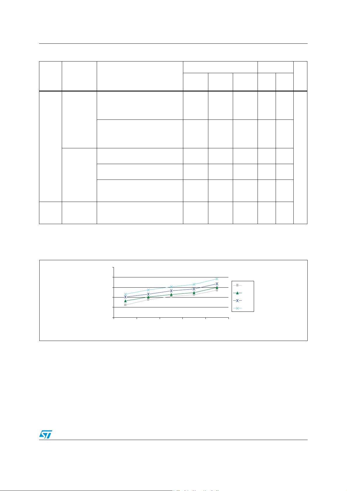
STM32F103x8, STM32F103xB Electrical characteristics
0
0.5
1
1.5
2
2.5
–40 °C 25 °C 70 °C 85 °C 105 °C
Temperature (°C)
Consumption ( µA )
2 V
2.4 V
3 V
3.6 V
ai17351
Table 16. Typical and maximum current consumptions in Stop and Standby modes
Symbol Parameter Conditions
(1)
Typ
V
DD/VBAT
= 2.0 V
VDD/V
= 2.4 V
BAT
VDD/V
= 3.3 V
BAT
TA =
85 °C
Regulator in Run mode, low-speed
I
DD
Supply current
in Stop mode
Supply current
in Standby
mode
and high-speed internal RC
oscillators and high-speed oscillator
OFF (no independent watchdog)
Regulator in Low Power mode, lowspeed and high-speed internal RC
oscillators and high-speed oscillator
OFF (no independent watchdog)
Low-speed internal RC oscillator and
independent watchdog ON
Low-speed internal RC oscillator
ON, independent watchdog OFF
Low-speed internal RC oscillator and
independent watchdog OFF, low-
- 23.5 24 200 370
- 13.5 14 180 340
-2.63.4--
-2.43.2--
-1.7245
speed oscillator and RTC OFF
I
DD_VBAT
Backup
domain supply
Low-speed oscillator and RTC ON 0.9 1.1 1.4 1.9
(2)
current
1. Typical values are measured at TA = 25 °C.
2. Based on characterization, not tested in production.
Max
TA =
105 °C
2.2
Unit
µA
Figure 17. Typical current consumption on V
V
values
BAT
with RTC on versus temperature at different
BAT
Doc ID 13587 Rev 13 43/99

Electrical characteristics STM32F103x8, STM32F103xB
0
50
100
150
200
250
300
-45 25 70 90 110
Temperature (°C)
Consumption (µA)
3.3 V
3.6 V
0
50
100
150
200
250
300
-40 0 25 70 85 105
Temperature (°C)
Consumption (µA)
3.3 V
3.6 V
Figure 18. Typical current consumption in Stop mode with regulator in Run mode versus
temperature at V
= 3.3 V and 3.6 V
DD
Figure 19. Typical current consumption in Stop mode with regulator in Low-power mode versus
temperature at V
= 3.3 V and 3.6 V
DD
44/99 Doc ID 13587 Rev 13

STM32F103x8, STM32F103xB Electrical characteristics
0
0.5
1
1.5
2
2.5
3
3.5
4
4.5
–45 °C 25 °C 85 °C 105 °C
Temperature (°C)
Consumption (µA)
3.3 V
3.6 V
Figure 20. Typical current consumption in Standby mode versus temperature at
V
= 3.3 V and 3.6 V
DD
Typical current consumption
The MCU is placed under the following conditions:
● All I/O pins are in input mode with a static value at V
● All peripherals are disabled except if it is explicitly mentioned.
● The Flash access time is adjusted to f
frequency (0 wait state from 0 to 24 MHz, 1
HCLK
wait state from 24 to 48 MHz and 2 wait states above).
● Ambient temperature and V
● Prefetch is ON (Reminder: this bit must be set before clock setting and bus prescaling)
● When the peripherals are enabled f
f
/4
PCLK2
supply voltage conditions summarized in Tab le 9 .
DD
= f
PCLK1
HCLK
or VSS (no load).
DD
/4, f
PCLK
2 = f
HCLK
/2, f
ADCCLK
=
Doc ID 13587 Rev 13 45/99

Electrical characteristics STM32F103x8, STM32F103xB
Table 17. Typical current consumption in Run mode, code with data processing
running from Flash
(1)
Typ
Symbol Parameter Conditions f
HCLK
All peripherals
enabled
(2)
All peripherals
disabled
72 MHz 36 27
48 MHz 24.2 18.6
36 MHz 19 14.8
24 MHz 12.9 10.1
16 MHz 9.3 7.4
External clock
(3)
8 MHz 5.5 4.6
4 MHz 3.3 2.8
2 MHz 2.2 1.9
1 MHz 1.6 1.45
500 kHz 1.3 1.25
I
DD
Supply
current in
Run mode
125 kHz 1.08 1.06
64 MHz 31.4 23.9
48 MHz 23.5 17.9
36 MHz 18.3 14.1
Running on high
speed internal RC
(HSI), AHB
prescaler used to
reduce the
frequency
24 MHz 12.2 9.5
16 MHz 8.5 6.8
8 MHz 4.9 4
4 MHz 2.7 2.2
2 MHz 1.6 1.4
1 MHz 1.02 0.9
500 kHz 0.73 0.67
125 kHz 0.5 0.48
1. Typical values are measures at TA = 25 °C, VDD = 3.3 V.
2. Add an additional power consumption of 0.8 mA per ADC for the analog part. In applications, this
consumption occurs only while the ADC is on (ADON bit is set in the ADC_CR2 register).
3. External clock is 8 MHz and PLL is on when f
HCLK
> 8 MHz.
Unit
mA
mA
46/99 Doc ID 13587 Rev 13

STM32F103x8, STM32F103xB Electrical characteristics
Table 18. Typical current consumption in Sleep mode, code running from Flash or
RAM
(1)
Typ
Symbol Parameter Conditions f
72 MHz 14.4 5.5
48 MHz 9.9 3.9
36 MHz 7.6 3.1
24 MHz 5.3 2.3
16 MHz 3.8 1.8
External clock
(3)
8 MHz 2.1 1.2
4 MHz 1.6 1.1
2 MHz 1.3 1
1 MHz 1.11 0.98
500 kHz 1.04 0.96
I
DD
Supply
current in
Sleep mode
125 kHz 0.98 0.95
64 MHz 12.3 4.4
48 MHz 9.3 3.3
HCLK
All peripherals
enabled
(2)
All peripherals
disabled
Unit
mA
36 MHz 7 2.5
24 MHz 4.8 1.8
Running on high
speed internal RC
(HSI), AHB prescaler
used to reduce the
frequency
16 MHz 3.2 1.2
8 MHz 1.6 0.6
4 MHz 1 0.5
2 MHz 0.72 0.47
1 MHz 0.56 0.44
500 kHz 0.49 0.42
125 kHz 0.43 0.41
1. Typical values are measures at TA = 25 °C, VDD = 3.3 V.
2. Add an additional power consumption of 0.8 mA per ADC for the analog part. In applications, this
consumption occurs only while the ADC is on (ADON bit is set in the ADC_CR2 register).
3. External clock is 8 MHz and PLL is on when f
HCLK
> 8 MHz.
Doc ID 13587 Rev 13 47/99

Electrical characteristics STM32F103x8, STM32F103xB
On-chip peripheral current consumption
The current consumption of the on-chip peripherals is given in Ta bl e 1 9. The MCU is placed
under the following conditions:
● all I/O pins are in input mode with a static value at V
● all peripherals are disabled unless otherwise mentioned
● the given value is calculated by measuring the current consumption
– with all peripherals clocked off
– with only one peripheral clocked on
● ambient operating temperature and V
supply voltage conditions summarized in
DD
Ta bl e 6
Table 19. Peripheral current consumption
(1)
Peripheral Typical consumption at 25 °C Unit
TIM2 1.2
TIM3 1.2
TIM4 0.9
SPI2 0.2
APB1
USART2 0.35
USART3 0.35
I2C1 0.39
I2C2 0.39
or VSS (no load)
DD
mA
USB 0.65
CAN 0.72
GPIO A 0.47
GPIO B 0.47
GPIO C 0.47
GPIO D 0.47
GPIO E 0.47
APB2
ADC1
ADC2 1.78
TIM1 1.6
SPI1 0.43
USART1 0.85
1. f
2. Specific conditions for ADC: f
= 72 MHz, f
HCLK
in the ADC_CR2 register is set to 1.
APB1
= f
HCLK
(2)
/2, f
HCLK
= f
APB2
HCLK
= 56 MHz, f
1.81
, default prescaler value for each peripheral.
= f
/2, f
= f
APB1
HCLK
APB2
HCLK
, f
ADCCLK
= f
APB2/4
mA
, ADON bit
48/99 Doc ID 13587 Rev 13

STM32F103x8, STM32F103xB Electrical characteristics
5.3.6 External clock source characteristics
High-speed external user clock generated from an external source
The characteristics given in Tab l e 2 0 result from tests performed using an high-speed
external clock source, and under ambient temperature and supply voltage conditions
summarized in Ta bl e 9 .
Table 20. High-speed external user clock characteristics
Symbol Parameter Conditions Min Typ Max Unit
f
HSE_ext
V
HSEH
V
HSEL
t
w(HSE)
t
w(HSE)
t
r(HSE)
t
f(HSE)
C
in(HSE)
DuCy
I
1. Guaranteed by design, not tested in production.
User external clock source
frequency
(1)
OSC_IN input pin high level voltage 0.7V
OSC_IN input pin low level voltage V
OSC_IN high or low time
OSC_IN rise or fall time
OSC_IN input capacitance
Duty cycle 45 55 %
(HSE)
OSC_IN Input leakage current VSS≤ VIN≤ V
L
(1)
(1)
(1)
DD
1825MHz
DD
SS
5
5pF
V
DD
0.3V
DD
20
±1 µA
Low-speed external user clock generated from an external source
The characteristics given in Tab l e 2 1 result from tests performed using an low-speed
external clock source, and under ambient temperature and supply voltage conditions
summarized in Ta bl e 9 .
Table 21. Low-speed external user clock characteristics
Symbol Parameter Conditions Min Typ Max Unit
V
ns
f
LSE_ext
V
LSEH
V
LSEL
t
w(LSE)
t
w(LSE)
t
r(LSE)
t
f(LSE)
C
in(LSE)
DuCy
1. Guaranteed by design, not tested in production.
User External clock source
frequency
(1)
OSC32_IN input pin high level
voltage
OSC32_IN input pin low level
voltage
OSC32_IN high or low time
OSC32_IN rise or fall time
OSC32_IN input capacitance
Duty cycle 30 70 %
(LSE)
OSC32_IN Input leakage
I
L
current
(1)
(1)
(1)
Doc ID 13587 Rev 13 49/99
V
SS
≤ VIN≤ V
DD
0.7V
V
450
32.768 1000 kHz
DD
SS
5pF
V
DD
0.3V
DD
50
±1 µA
V
ns

Electrical characteristics STM32F103x8, STM32F103xB
ai14143
OS C _I N
EXTERNAL
STM32F103xx
CLOCK SO URCE
V
HSEH
t
f(HSE)
t
W(HSE)
I
L
90%
10%
T
HSE
t
t
r(HSE)
t
W(HSE)
f
HSE_ext
V
HSEL
ai14144b
OSC32_IN
EXTERNAL
STM32F103xx
CLOCK SO URCE
V
LSEH
t
f(LSE)
t
W(LSE)
I
L
90%
10%
T
LSE
t
t
r(LSE)
t
W(LSE)
f
LSE_ext
V
LSEL
Figure 21. High-speed external clock source AC timing diagram
Figure 22. Low-speed external clock source AC timing diagram
High-speed external clock generated from a crystal/ceramic resonator
The high-speed external (HSE) clock can be supplied with a 4 to 16 MHz crystal/ceramic
resonator oscillator. All the information given in this paragraph are based on characterization
results obtained with typical external components specified in Ta bl e 2 2. In the application,
the resonator and the load capacitors have to be placed as close as possible to the oscillator
pins in order to minimize output distortion and startup stabilization time. Refer to the crystal
resonator manufacturer for more details on the resonator characteristics (frequency,
package, accuracy).
50/99 Doc ID 13587 Rev 13
STM32F103x8, STM32F103xB Electrical characteristics
ai14145
OSC_OUT
OSC_IN
f
HSE
C
L1
R
F
STM32F103xx
8 MHz
resonator
R
EXT
(1)
C
L2
Resonator with
integrated capacitors
Bias
controlled
gain
Table 22. HSE 4-16 MHz oscillator characteristics
(1) (2)
Symbol Parameter Conditions Min Typ Max Unit
f
OSC_IN
R
Oscillator frequency 4 8 16 MHz
Feedback resistor 200 kΩ
F
Recommended load capacitance
C
versus equivalent serial
resistance of the crystal (R
i
HSE driving current
2
g
t
SU(HSE
1. Resonator characteristics given by the crystal/ceramic resonator manufacturer.
2. Based on characterization, not tested in production.
3. The relatively low value of the RF resistor offers a good protection against issues resulting from use in a
humid environment, due to the induced leakage and the bias condition change. However, it is
recommended to take this point into account if the MCU is used in tough humidity conditions.
4. t
SU(HSE)
oscillation is reached. This value is measured for a standard crystal resonator and it can vary significantly
with the crystal manufacturer
Oscillator transconductance Startup 25 mA/V
m
(4)
startup time VDD is stabilized 2 ms
is the startup time measured from the moment it is enabled (by software) to a stabilized 8 MHz
(3)
)
S
RS = 30 Ω 30 pF
= 3.3 V, VIN=V
V
DD
SS
with 30 pF load
1mA
For CL1 and CL2, it is recommended to use high-quality external ceramic capacitors in the
5 pF to 25 pF range (typ.), designed for high-frequency applications, and selected to match
the requirements of the crystal or resonator (see Figure 23). C
and C
L1
are usually the
L2
same size. The crystal manufacturer typically specifies a load capacitance which is the
series combination of C
and CL2. PCB and MCU pin capacitance must be included (10 pF
L1
can be used as a rough estimate of the combined pin and board capacitance) when sizing
C
and CL2. Refer to the application note AN2867 “Oscillator design guide for ST
L1
microcontrollers” available from the ST website www.st.com.
Figure 23. Typical application with an 8 MHz crystal
1. R
value depends on the crystal characteristics.
EXT
Low-speed external clock generated from a crystal/ceramic resonator
The low-speed external (LSE) clock can be supplied with a 32.768 kHz crystal/ceramic
resonator oscillator. All the information given in this paragraph are based on characterization
results obtained with typical external components specified in Ta bl e 2 3. In the application,
the resonator and the load capacitors have to be placed as close as possible to the oscillator
pins in order to minimize output distortion and startup stabilization time. Refer to the crystal
resonator manufacturer for more details on the resonator characteristics (frequency,
package, accuracy).
Doc ID 13587 Rev 13 51/99

Electrical characteristics STM32F103x8, STM32F103xB
Table 23. LSE oscillator characteristics (f
= 32.768 kHz)
LSE
(1) (2)
Symbol Parameter Conditions Min Typ Max Unit
R
F
Feedback resistor 5 MΩ
Recommended load capacitance
R
C
I
2
g
m
versus equivalent serial
resistance of the crystal (R
)
S
LSE driving current
Oscillator transconductance 5 µA/V
= 30 KΩ 15 pF
S
= 3.3 V
V
DD
VIN = V
SS
1.4 µA
TA = 50 °C 1.5
T
= 25 °C 2.5
A
T
= 10 °C 4
A
= 0 °C 6
T
is
t
1. Based on characterization, not tested in production.
2. Refer to the note and caution paragraphs below the table, and to the application note AN2867 “Oscillator design guide for
3. t
(3)
SU(LSE)
ST microcontrollers”.
SU(LSE)
reached. This value is measured for a standard crystal and it can vary significantly with the crystal manufacturer
Startup time
is the startup time measured from the moment it is enabled (by software) to a stabilized 32.768 kHz oscillation is
V
DD
stabilized
A
= -10 °C 10
T
A
T
= -20 °C 17
A
= -30 °C 32
T
A
T
= -40 °C 60
A
s
Note: For CL1 and C
it is recommended to use high-quality ceramic capacitors in the 5 pF to
L2
15 pF range selected to match the requirements of the crystal or resonator. C
usually the same size. The crystal manufacturer typically specifies a load capacitance which
is the series combination of C
Load capacitance C
C
is the pin capacitance and board or trace PCB-related capacitance. Typically, it is
stray
has the following formula: CL = CL1 x CL2 / (CL1 + CL2) + C
L
and CL2.
L1
between 2 pF and 7 pF.
Caution: To avoid exceeding the maximum value of C
to use a resonator with a load capacitance C
capacitance of 12.5 pF.
Example: if you choose a resonator with a load capacitance of C
then C
= CL2 = 8 pF.
L1
and C
L1
and CL2 (15 pF) it is strongly recommended
L1
≤
7 pF. Never use a resonator with a load
L
= 6 pF, and C
L
stray
stray
L2,
where
= 2 pF,
are
52/99 Doc ID 13587 Rev 13

STM32F103x8, STM32F103xB Electrical characteristics
ai14146
OSC32_OUT
OSC32_IN
f
LSE
C
L1
R
F
STM32F103xx
32.768 kHz
resonator
C
L2
Resonator with
integrated capacitors
Bias
controlled
gain
Figure 24. Typical application with a 32.768 kHz crystal
5.3.7 Internal clock source characteristics
The parameters given in Tab l e 2 4 are derived from tests performed under ambient
temperature and V
High-speed internal (HSI) RC oscillator
Table 24. HSI oscillator characteristics
supply voltage conditions summarized in Tab l e 9 .
DD
(1)
Symbol Parameter Conditions Min Typ Max Unit
f
HSI
DuCy
ACC
t
su(HSI)
I
DD(HSI)
1. V
DD
2. Refer to application note AN2868 “STM32F10xxx internal RC oscillator (HSI) calibration” available from
the ST website www.st.com.
3. Guaranteed by design, not tested in production.
4. Based on characterization, not tested in production.
Frequency 8 MHz
Duty cycle 45 55 %
(HSI)
User-trimmed with the RCC_CR
register
Accuracy of the HSI
HSI
oscillator
Factorycalibrated
HSI oscillator
(4)
startup time
HSI oscillator power
(4)
consumption
= 3.3 V, TA = –40 to 105 °C unless otherwise specified.
(2)
TA = –40 to 105 °C –2 2.5 %
= –10 to 85 °C –1.5 2.2 %
T
A
(4)
T
= 0 to 70 °C –1.3 2 %
A
= 25 °C –1.1 1.8 %
T
A
12µs
80 100 µA
(3)
1
%
Doc ID 13587 Rev 13 53/99
Electrical characteristics STM32F103x8, STM32F103xB
Low-speed internal (LSI) RC oscillator
Table 25. LSI oscillator characteristics
(1)
Symbol Parameter
(2)
f
LSI
t
su(LSI)
I
DD(LSI)
= 3 V, TA = –40 to 105 °C unless otherwise specified.
1. V
DD
2. Based on characterization, not tested in production.
3. Guaranteed by design, not tested in production.
Frequency 30 40 60 kHz
(3)
LSI oscillator startup time 85 µs
(3)
LSI oscillator power consumption 0.65 1.2 µA
Min
Typ M ax Unit
Wakeup time from low-power mode
The wakeup times given in Ta bl e 2 6 is measured on a wakeup phase with a 8-MHz HSI RC
oscillator. The clock source used to wake up the device depends from the current operating
mode:
● Stop or Standby mode: the clock source is the RC oscillator
● Sleep mode: the clock source is the clock that was set before entering Sleep mode.
All timings are derived from tests performed under ambient temperature and V
voltage conditions summarized in Tabl e 9 .
supply
DD
54/99 Doc ID 13587 Rev 13

STM32F103x8, STM32F103xB Electrical characteristics
Table 26. Low-power mode wakeup timings
Symbol Parameter Typ Unit
t
WUSLEEP
(1)
Wakeup from Sleep mode 1.8 µs
Wakeup from Stop mode (regulator in run mode) 3.6
t
WUSTOP
(1)
Wakeup from Stop mode (regulator in low power
mode)
t
WUSTDBY
1. The wakeup times are measured from the wakeup event to the point in which the user application code
reads the first instruction.
(1)
Wakeup from Standby mode 50 µs
5.3.8 PLL characteristics
The parameters given in Tab l e 2 7 are derived from tests performed under ambient
temperature and V
Table 27. PLL characteristics
Symbol Parameter
f
PLL_IN
f
PLL_OUT
t
LOCK
Jitter Cycle-to-cycle jitter 300 ps
1. Based on characterization, not tested in production.
2. Take care of using the appropriate multiplier factors so as to have PLL input clock values compatible with
the range defined by f
supply voltage conditions summarized in Tab l e 9 .
DD
PLL input clock
PLL input clock duty cycle 40 60 %
PLL multiplier output clock 16 72 MHz
PLL lock time 200 µs
PLL_OUT
5.4
µs
Val ue
(1)
Min
(2)
.
18.0 25 MHz
Typ Max
(1)
Unit
5.3.9 Memory characteristics
Flash memory
The characteristics are given at TA = –40 to 105 °C unless otherwise specified.
Table 28. Flash memory characteristics
Symbol Parameter Conditions Min
t
t
ERASE
t
16-bit programming time TA = –40 to +105 °C 40 52.5 70 µs
prog
Page (1 KB) erase time TA = –40 to +105 °C 20 40 ms
Mass erase time TA = –40 to +105 °C 20 40 ms
ME
(1)
Typ Max
(1)
Unit
Doc ID 13587 Rev 13 55/99
Electrical characteristics STM32F103x8, STM32F103xB
Table 28. Flash memory characteristics (continued)
Symbol Parameter Conditions Min
Read mode
= 72 MHz with 2 wait
f
HCLK
states, VDD = 3.3 V
I
DD
Supply current
Write / Erase modes
= 72 MHz, VDD = 3.3 V
f
HCLK
Power-down mode / Halt,
= 3.0 to 3.6 V
V
DD
V
1. Guaranteed by design, not tested in production.
Programming voltage 2 3.6 V
prog
(1)
Typ Max
(1)
Unit
20 mA
5mA
50 µA
Table 29. Flash memory endurance and data retention
Val ue
Symbol Parameter Conditions
= –40 to +85 °C (6 suffix versions)
T
N
END
t
RET
Endurance
Data retention
A
T
= –40 to +105 °C (7 suffix versions)
A
1 kcycle
10 kcycles
(2)
at TA = 85 °C
(2)
at TA = 105 °C 10
(2)
at TA = 55 °C 20
Min
30
(1)
10
Typ Max
Unit
kcycles
Years1 kcycle
1. Based on characterization, not tested in production.
2. Cycling performed over the whole temperature range.
5.3.10 EMC characteristics
Susceptibility tests are performed on a sample basis during device characterization.
Functional EMS (electromagnetic susceptibility)
While a simple application is executed on the device (toggling 2 LEDs through I/O ports). the
device is stressed by two electromagnetic events until a failure occurs. The failure is
indicated by the LEDs:
● Electrostatic discharge (ESD) (positive and negative) is applied to all device pins until
a functional disturbance occurs. This test is compliant with the IEC 61000-4-2 standard.
● FTB: A Burst of Fast Transient voltage (positive and negative) is applied to V
V
through a 100 pF capacitor, until a functional disturbance occurs. This test is
SS
compliant with the IEC 61000-4-4 standard.
A device reset allows normal operations to be resumed.
The test results are given in Tab l e 3 0 . They are based on the EMS levels and classes
defined in application note AN1709.
DD
and
56/99 Doc ID 13587 Rev 13

STM32F103x8, STM32F103xB Electrical characteristics
Table 30. EMS characteristics
Symbol Parameter Conditions
= 3.3 V, TA = +25 °C,
V
V
V
FESD
EFTB
Voltage limits to be applied on any I/O pin to
induce a functional disturbance
Fast transient voltage burst limits to be
applied through 100 pF on VDD and V
SS
pins to induce a functional disturbance
DD
f
= 72 MHz
HCLK
conforms to IEC 61000-4-2
V
= 3.3 V, TA = +25 °C,
DD
f
= 72 MHz
HCLK
conforms to IEC 61000-4-4
Level/
Class
2B
4A
Designing hardened software to avoid noise problems
EMC characterization and optimization are performed at component level with a typical
application environment and simplified MCU software. It should be noted that good EMC
performance is highly dependent on the user application and the software in particular.
Therefore it is recommended that the user applies EMC software optimization and
prequalification tests in relation with the EMC level requested for his application.
Software recommendations
The software flowchart must include the management of runaway conditions such as:
● Corrupted program counter
● Unexpected reset
● Critical Data corruption (control registers...)
Prequalification trials
Most of the common failures (unexpected reset and program counter corruption) can be
reproduced by manually forcing a low state on the NRST pin or the Oscillator pins for 1
second.
To complete these trials, ESD stress can be applied directly on the device, over the range of
specification values. When unexpected behavior is detected, the software can be hardened
to prevent unrecoverable errors occurring (see application note AN1015).
Electromagnetic Interference (EMI)
The electromagnetic field emitted by the device are monitored while a simple application is
executed (toggling 2 LEDs through the I/O ports). This emission test is compliant with
IEC 61967-2 standard which specifies the test board and the pin loading.
Table 31. EMI characteristics
Symbol Parameter Conditions
= 3.3 V, TA = 25 °C,
V
DD
S
EMI
Peak level
LQFP100 package
compliant with
IEC 61967-2
Monitored
frequency band
Max vs. [f
8/48 MHz 8/72 MHz
HSE/fHCLK
0.1 to 30 MHz 12 12
130 MHz to 1GHz 23 29
SAE EMI Level 4 4 -
]
Unit
dBµV30 to 130 MHz 22 19
Doc ID 13587 Rev 13 57/99
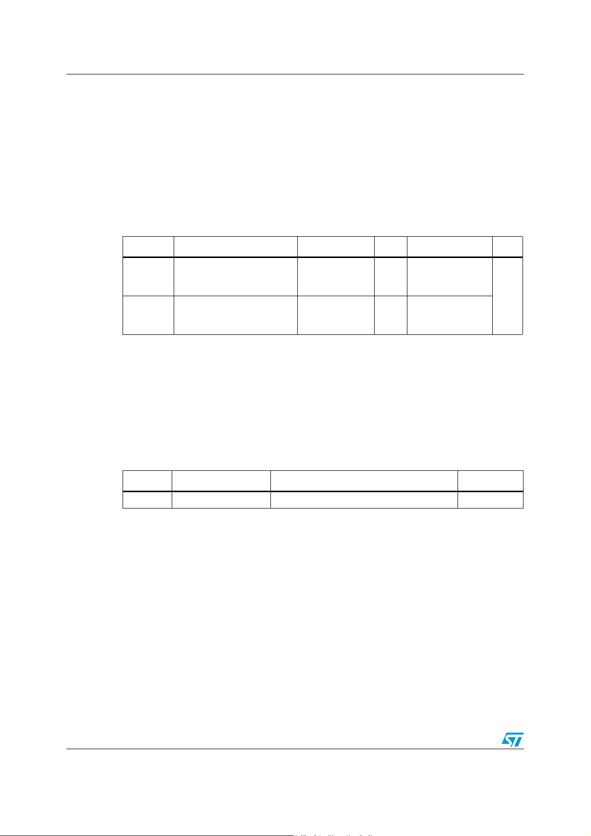
Electrical characteristics STM32F103x8, STM32F103xB
5.3.11 Absolute maximum ratings (electrical sensitivity)
Based on three different tests (ESD, LU) using specific measurement methods, the device is
stressed in order to determine its performance in terms of electrical sensitivity.
Electrostatic discharge (ESD)
Electrostatic discharges (a positive then a negative pulse separated by 1 second) are
applied to the pins of each sample according to each pin combination. The sample size
depends on the number of supply pins in the device (3 parts × (n+1) supply pins). This test
conforms to the JESD22-A114/C101 standard.
Table 32. ESD absolute maximum ratings
Symbol Ratings Conditions Class Maximum value
= +25 °C
T
V
ESD(HBM)
Electrostatic discharge
voltage (human body model)
Electrostatic discharge
V
ESD(CDM)
voltage (charge device
model)
1. Based on characterization results, not tested in production.
A
conforming to
JESD22-A114
TA = +25 °C
conforming to
JESD22-C101
2 2000
II 500
(1)
Unit
V
Static latch-up
Two complementary static tests are required on six parts to assess the latch-up
performance:
● A supply overvoltage is applied to each power supply pin
● A current injection is applied to each input, output and configurable I/O pin
These tests are compliant with EIA/JESD 78A IC latch-up standard.
Table 33. Electrical sensitivities
Symbol Parameter Conditions Class
LU Static latch-up class T
= +105 °C conforming to JESD78A II level A
A
58/99 Doc ID 13587 Rev 13
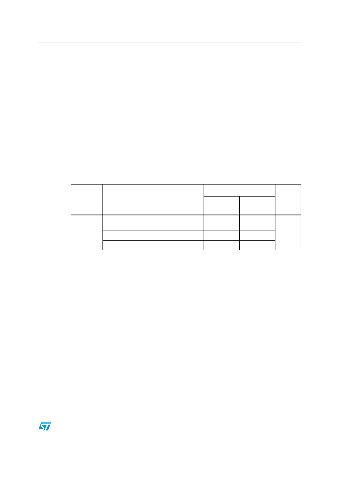
STM32F103x8, STM32F103xB Electrical characteristics
5.3.12 I/O current injection characteristics
As a general rule, current injection to the I/O pins, due to external voltage below VSS or
above V
operation. However, in order to give an indication of the robustness of the microcontroller in
cases when abnormal injection accidentally happens, susceptibility tests are performed on a
sample basis during device characterization.
Functional susceptibilty to I/O current injection
While a simple application is executed on the device, the device is stressed by injecting
current into the I/O pins programmed in floating input mode. While current is injected into the
I/O pin, one at a time, the device is checked for functional failures.
The failure is indicated by an out of range parameter: ADC error above a certain limit (>5
LSB TUE), out of spec current injection on adjacent pins or other functional failure (for
example reset, oscillator frequency deviation).
The test results are given in Tab l e 3 4
Table 34. I/O current injection susceptibility
Symbol Description
(for standard, 3 V-capable I/O pins) should be avoided during normal product
DD
Functional susceptibility
Negative
injection
Positive
injection
Unit
I
INJ
Injected current on OSC_IN32,
OSC_OUT32, PA4, PA5, PC13
Injected current on all FT pins -5 +0
Injected current on any other pin -5 +5
-0 +0
mA
Doc ID 13587 Rev 13 59/99

Electrical characteristics STM32F103x8, STM32F103xB
5.3.13 I/O port characteristics
General input/output characteristics
Unless otherwise specified, the parameters given in Ta bl e 3 5 are derived from tests
performed under the conditions summarized in Tab l e 9 . All I/Os are CMOS and TTL
compliant.
Table 35. I/O static characteristics
Symbol Parameter Conditions Min Typ Max Unit
Standard IO input low
level voltage
V
IL
IO FT
(1)
voltage
Standard IO input high
level voltage
V
IH
IO FT
(1)
voltage
input low level
input high level
–0.3 0.28*(V
–0.3 0.32*(V
0.41*(V
> 2 V
V
DD
V
≤ 2 V 5.2
DD
0.42*(V
-2 V)+1.3 V VDD+0.3 V
DD
-2 V)+1 V
DD
-2 V)+0.8 V V
DD
-2V)+0.75 V V
DD
5.5
Standard IO Schmitt
trigger voltage
hys
hysteresis
V
IO FT Schmitt trigger
voltage hysteresis
Input leakage current
I
lkg
(2)
(2)
V
Standard I/Os
(4)
≤ VIN≤ V
SS
V
IN
DD
= 5 V
I/O FT
R
R
1. FT = Five-volt tolerant. In order to sustain a voltage higher than VDD+0.3 the internal pull-up/pull-down resistors must be
2. Hysteresis voltage between Schmitt trigger switching levels. Based on characterization, not tested in production.
3. With a minimum of 100 mV.
4. Leakage could be higher than max. if negative current is injected on adjacent pins.
5. Pull-up and pull-down resistors are designed with a true resistance in series with a switchable PMOS/NMOS. This
Weak pull-up equivalent
PU
PD
C
IO
disabled.
PMOS/NMOS contribution
(5)
resistor
Weak pull-down
equivalent resistor
(5)
I/O pin capacitance 5 pF
to the series resistance is minimum (~10% order).
V
= V
IN
SS
V
= V
IN
DD
200 mV
DD
(3)
5% V
±1
3
30 40 50 kΩ
30 40 50 kΩ
V
mV
µA
60/99 Doc ID 13587 Rev 13

STM32F103x8, STM32F103xB Electrical characteristics
AIB
6$$6
)NPUTRANGE
NOTGUARANTEED
6
)(
6
$$
#-/3STANDARDREQUIREMENT6
)(
6
$$
6)(6),6
#-/3STANDARDREQUIREMENT6
),
6
$$
7
),MAX
7
)(MIN
6
$$
6
),
AI
)NPUTRANGE
NOTGUARANTEED
6)(6),6
44,REQUIREMENTS 6)(6
6
)(
6
$$
6
),
6
$$
44,REQUIREMENTS 6),6
6$$6
7
),MAX
7
)(MIN
All I/Os are CMOS and TTL compliant (no software configuration required). Their
characteristics cover more than the strict CMOS-technology or TTL parameters. The
coverage of these requirements is shown in Figure 25 and Figure 26 for standard I/Os, and
in Figure 27 and Figure 28 for 5 V tolerant I/Os.
Figure 25. Standard I/O input characteristics - CMOS port
Figure 26. Standard I/O input characteristics - TTL port
Doc ID 13587 Rev 13 61/99
Electrical characteristics STM32F103x8, STM32F103xB
6$$
#-/3STANDARDREQUIREMENTS6
)(
6
$$
#-/3STANDARDREQUIRMENT6
),
6
$$
6)(6),6
6$$6
)NPUTRANGE
NOTGUARANTEED
AIB
6
)(
6
$$
6
),
6
$$
NOTGUARANTEED
)NPUTRANGE
44,REQUIREMENT6)(6
6
)(
6
$$
6
),
6
$$
44,REQUIREMENTS6),6
6)(6),6
6$$6
7
),MAX
7
)(MIN
AI
Figure 27. 5 V tolerant I/O input characteristics - CMOS port
Figure 28. 5 V tolerant I/O input characteristics - TTL port
62/99 Doc ID 13587 Rev 13
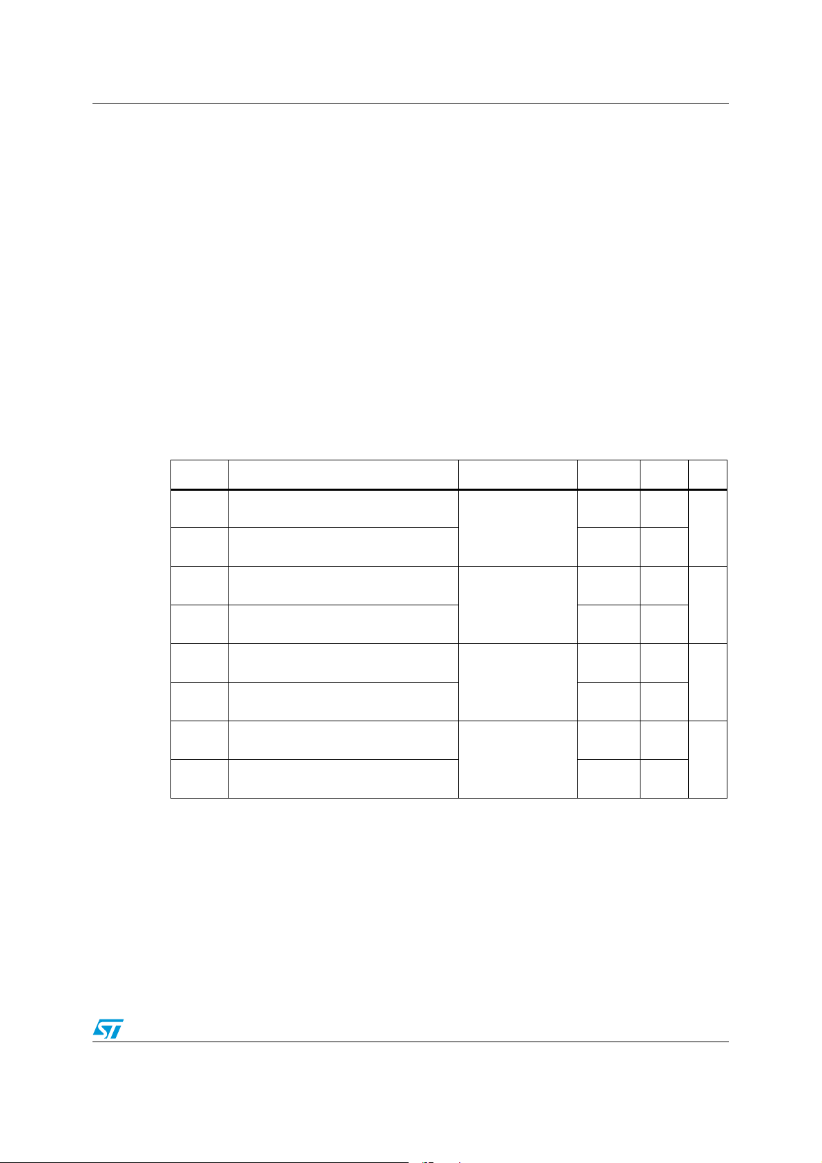
STM32F103x8, STM32F103xB Electrical characteristics
Output driving current
The GPIOs (general-purpose inputs/outputs) can sink or source up to ±8 mA, and sink or
source up to ±20 mA (with a relaxed V
OL/VOH
).
In the user application, the number of I/O pins which can drive current must be limited to
respect the absolute maximum rating specified in Section 5.2:
● The sum of the currents sourced by all the I/Os on V
consumption of the MCU sourced on V
I
(see Ta bl e 7 ).
VDD
● The sum of the currents sunk by all the I/Os on V
consumption of the MCU sunk on V
I
(see Ta bl e 7 ).
VSS
cannot exceed the absolute maximum rating
DD,
cannot exceed the absolute maximum rating
SS
SS
plus the maximum Run
DD,
plus the maximum Run
Output voltage levels
Unless otherwise specified, the parameters given in Ta bl e 3 6 are derived from tests
performed under ambient temperature and V
Ta bl e 9 . All I/Os are CMOS and TTL compliant.
Table 36. Output voltage characteristics
Symbol Parameter Conditions Min Max Unit
supply voltage conditions summarized in
DD
Output low level voltage for an I/O pin
(1)
V
OL
V
OH
V
OL
V
OH
V
OL
V
OH
V
OL
V
OH
1. The IIO current sunk by the device must always respect the absolute maximum rating specified in Table 7
and the sum of I
2. TTL and CMOS outputs are compatible with JEDEC standards JESD36 and JESD52.
3. The IIO current sourced by the device must always respect the absolute maximum rating specified in
Table 7 and the sum of I
4. Based on characterization data, not tested in production.
when 8 pins are sunk at same time
Output high level voltage for an I/O pin
(3)
when 8 pins are sourced at same time
Output low level voltage for an I/O pin
(1)
when 8 pins are sunk at same time
Output high level voltage for an I/O pin
(3)
when 8 pins are sourced at same time
Output low level voltage for an I/O pin
(1)(4)
when 8 pins are sunk at same time
Output high level voltage for an I/O pin
(3)(4)
when 8 pins are sourced at same time
Output low level voltage for an I/O pin
(1)(4)
when 8 pins are sunk at same time
Output high level voltage for an I/O pin
(3)(4)
when 8 pins are sourced at same time
(I/O ports and control pins) must not exceed I
IO
(I/O ports and control pins) must not exceed I
IO
CMOS port
I
IO
2.7 V < V
TTL port
I
IO
2.7 V < V
I
= +20 mA
IO
2.7 V < V
I
IO
2 V < VDD < 2.7 V
= +8 mA
< 3.6 V
DD
(2)
=+ 8mA
< 3.6 V
DD
< 3.6 V
DD
= +6 mA
.
VSS
(2)
VDD
,
–0.4
V
DD
0.4
0.4
2.4
1.3
–1.3
V
DD
0.4
–0.4
V
DD
.
V
V
V
V
Doc ID 13587 Rev 13 63/99

Electrical characteristics STM32F103x8, STM32F103xB
Input/output AC characteristics
The definition and values of input/output AC characteristics are given in Figure 29 and
Ta bl e 3 7, respectively.
Unless otherwise specified, the parameters given in Ta bl e 3 7 are derived from tests
performed under the ambient temperature and V
in Ta bl e 9 .
Table 37. I/O AC characteristics
(1)
supply voltage conditions summarized
DD
MODEx[1:0]
bit value
10
01
11
Symbol Parameter Conditions Min Max Unit
(1)
f
max(IO)out
t
f(IO)out
t
r(IO)out
f
max(IO)out
t
f(IO)out
t
r(IO)out
F
max(IO)out
t
f(IO)out
t
r(IO)out
Maximum frequency
Output high to low
level fall time
Output low to high
level rise time
Maximum frequency
Output high to low
level fall time
Output low to high
level rise time
Maximum frequency
Output high to low
level fall time
Output low to high
level rise time
(2)
CL = 50 pF, V
= 50 pF, V
C
L
(2)
CL = 50 pF, V
= 50 pF, V
C
L
CL = 30 pF, V
(2)
= 50 pF, VDD = 2.7 V to 3.6 V 30 MHz
C
L
= 50 pF, V
C
L
= 30 pF, V
C
L
= 50 pF, V
C
L
CL = 50 pF, V
= 30 pF, V
C
L
CL = 50 pF, V
CL = 50 pF, V
= 2 V to 3.6 V 2 MHz
DD
= 2 V to 3.6 V
DD
= 2 V to 3.6 V 10 MHz
DD
= 2 V to 3.6 V
DD
= 2.7 V to 3.6 V 50 MHz
DD
= 2 V to 2.7 V 20 MHz
DD
= 2.7 V to 3.6 V 5
DD
= 2.7 V to 3.6 V 8
DD
= 2 V to 2.7 V 12
DD
= 2.7 V to 3.6 V 5
DD
= 2.7 V to 3.6 V 8
DD
= 2 V to 2.7 V 12
DD
125
125
25
25
(3)
(3)
(3)
(3)
(3)
(3)
(3)
(3)
(3)
(3)
Pulse width of
-t
EXTIpw
external signals
detected by the EXTI
10 ns
controller
1. The I/O speed is configured using the MODEx[1:0] bits. Refer to the STM32F10xxx reference manual for a
description of GPIO Port configuration register.
2. The maximum frequency is defined in Figure 29.
3. Guaranteed by design, not tested in production.
ns
ns
ns
64/99 Doc ID 13587 Rev 13

STM32F103x8, STM32F103xB Electrical characteristics
Figure 29. I/O AC characteristics definition
External
Output
on 50pF
Maximum frequency is achieved if (tr + tf) ≤ 2/3)T and if the duty cycle is (45-55%)
t
r(IO)out
5.3.14 NRST pin characteristics
The NRST pin input driver uses CMOS technology. It is connected to a permanent pull-up
resistor, R
Unless otherwise specified, the parameters given in Ta bl e 3 8 are derived from tests
performed under the ambient temperature and V
in Ta bl e 9 .
Table 38. NRST pin characteristics
Symbol Parameter Conditions Min Typ Max Unit
V
IL(NRST)
V
IH(NRST)
V
hys(NRST)
R
V
F(NRST)
V
NF(NRST)
1. Guaranteed by design, not tested in production.
2. The pull-up is designed with a true resistance in series with a switchable PMOS. This PMOS contribution
to the series resistance must be minimum (~10% order).
(see Ta bl e 3 5).
PU
(1)
(1)
PU
(1)
(1)
NRST Input low level voltage –0.5 0.8
NRST Input high level voltage 2 VDD+0.5
NRST Schmitt trigger voltage
hysteresis
Weak pull-up equivalent resistor
NRST Input filtered pulse 100 ns
NRST Input not filtered pulse 300 ns
90%
50%
10%
when loaded by 50 pF
(2)
10 %
50%
90%
t
r(IO)out
T
supply voltage conditions summarized
DD
200 mV
V
IN
= V
SS
30 40 50 kΩ
ai14131
V
Doc ID 13587 Rev 13 65/99

Electrical characteristics STM32F103x8, STM32F103xB
Figure 30. Recommended NRST pin protection
V
(2)
DD
R
PU
Filter
Internal reset
External
reset circuit
(1)
NRST
0.1 µF
STM32F10x
ai14132d
2. The reset network protects the device against parasitic resets.
3. The user must ensure that the level on the NRST pin can go below the V
Table 38. Otherwise the reset will not be taken into account by the device.
max level specified in
IL(NRST)
5.3.15 TIM timer characteristics
The parameters given in Tab l e 3 9 are guaranteed by design.
Refer to Section 5.3.12: I/O current injection characteristics for details on the input/output
alternate function characteristics (output compare, input capture, external clock, PWM
output).
Table 39. TIMx
(1)
characteristics
Symbol Parameter Conditions Min Max Unit
1
t
res(TIM)
f
EXT
Res
t
COUNTER
Timer resolution time
f
Timer external clock
frequency on CH1 to CH4
Timer resolution 16 bit
TIM
0
f
TIMxCLK
16-bit counter clock period
TIMxCLK
= 72 MHz
= 72 MHz
13.9 ns
f
TIMxCLK
036MHz
1 65536
when internal clock is
selected
f
TIMxCLK
= 72 MHz
0.0139 910 µs
/2
65536 × 65536
t
MAX_COUNT
1. TIMx is used as a general term to refer to the TIM1, TIM2, TIM3 and TIM4 timers.
Maximum possible count
f
TIMxCLK
= 72 MHz
59.6 s
t
TIMxCLK
MHz
t
TIMxCLK
t
TIMxCLK
66/99 Doc ID 13587 Rev 13

STM32F103x8, STM32F103xB Electrical characteristics
5.3.16 Communications interfaces
I2C interface characteristics
Unless otherwise specified, the parameters given in Ta bl e 4 0 are derived from tests
performed under the ambient temperature, f
conditions summarized in Ta bl e 9 .
2
The STM32F103xx performance line
2
I
C communication protocol with the following restrictions: the I/O pins SDA and SCL are
I
C interface meets the requirements of the standard
mapped to are not “true” open-drain. When configured as open-drain, the PMOS connected
between the I/O pin and V
2
The I
C characteristics are described in Ta b le 4 0 . Refer also to Section 5.3.12: I/O current
injection characteristics
(SDA and SCL)
Table 40. I2C characteristics
Symbol Parameter
.
is disabled, but is still present.
DD
for more details on the input/output alternate function characteristics
Standard mode I
Min Max Min Max
frequency and VDD supply voltage
PCLK1
2C(1)
Fast mode I2C
(1)(2)
Unit
t
w(SCLL)
t
w(SCLH)
t
su(SDA)
t
h(SDA)
t
r(SDA)
t
r(SCL)
t
f(SDA)
t
f(SCL)
t
h(STA)
t
su(STA)
t
su(STO)
t
w(STO:STA)
C
Guaranteed by design, not tested in production.
1.
2. f
PCLK1
4 MHz to achieve fast mode I
maximum I2C fast mode clock.
The maximum hold time of the Start condition has only to be met if the interface does not stretch the low
3.
period of SCL signal.
The device must internally provide a hold time of at least 300ns for the SDA signal in order to bridge the
4.
undefined region of the falling edge of SCL.
SCL clock low time 4.7 1.3
SCL clock high time 4.0 0.6
SDA setup time 250 100
SDA data hold time 0
(3)
SDA and SCL rise time 1000 20 + 0.1C
(4)
0
900
300
b
SDA and SCL fall time 300 300
Start condition hold time 4.0 0.6
Repeated Start condition
setup time
4.7 0.6
Stop condition setup time 4.0 0.6 μs
Stop to Start condition time
(bus free)
Capacitive load for each bus
b
line
must be higher than 2 MHz to achieve standard mode I2C frequencies. It must be higher than
2
C frequencies. It must be a multiple of 10 MHz to reach the 400 kHz
4.7 1.3 μs
400 400 pF
µs
(3)
ns
µs
Doc ID 13587 Rev 13 67/99
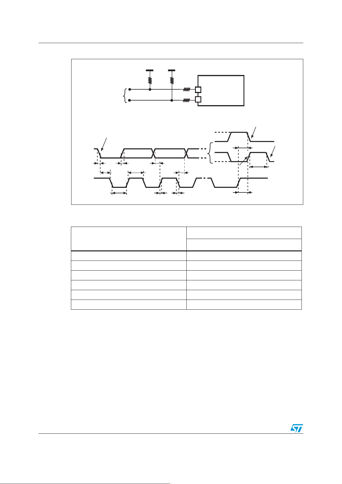
Electrical characteristics STM32F103x8, STM32F103xB
ai14133d
Start
SDA
100 Ω
4.7kΩ
I²C bus
4.7kΩ
100 Ω
V
DD
V
DD
STM32F10x
SDA
SCL
t
f(SDA)
t
r(SDA)
SCL
t
h(STA)
t
w(SCLH)
t
w(SCLL)
t
su(SDA)
t
r(SCL)
t
f(SCL)
t
h(SDA)
Start repeated
Start
t
su(STA)
t
su(STO)
Stop
t
su(STO:STA)
Figure 31. I2C bus AC waveforms and measurement circuit
Measurement points are done at CMOS levels: 0.3V
1.
Table 41. SCL frequency (f
= 36 MHz.,VDD = 3.3 V)
PCLK1
and 0.7VDD.
DD
(1)(2)
I2C_CCR value
f
(kHz)
SCL
R
= 4.7 kΩ
P
400 0x801E
300 0x8028
200 0x803C
100 0x00B4
50 0x0168
20 0x0384
= External pull-up resistance, f
1. R
P
2. For speeds around 200 kHz, the tolerance on the achieved speed is of ±5%. For other speed ranges, the
tolerance on the achieved speed ±2%. These variations depend on the accuracy of the external
components used to design the application.
= I2C speed,
SCL
68/99 Doc ID 13587 Rev 13

STM32F103x8, STM32F103xB Electrical characteristics
SPI interface characteristics
Unless otherwise specified, the parameters given in Ta bl e 4 2 are derived from tests
performed under the ambient temperature, f
conditions summarized in Ta bl e 9 .
Refer to Section 5.3.12: I/O current injection characteristics for more details on the
input/output alternate function characteristics (NSS, SCK, MOSI, MISO).
Table 42. SPI characteristics
Symbol Parameter Conditions Min Max Unit
frequency and VDD supply voltage
PCLKx
f
SCK
1/t
c(SCK)
t
r(SCK)
t
f(SCK)
DuCy(SCK)
t
su(NSS)
t
h(NSS)
t
w(SCKH)
t
w(SCKL)
t
su(MI)
t
su(SI)
t
h(MI)
t
h(SI)
t
a(SO)
t
dis(SO)
t
v(SO)
t
v(MO)
t
h(SO)
t
h(MO)
1. Based on characterization, not tested in production.
2. Min time is for the minimum time to drive the output and the max time is for the maximum time to validate
the data.
3. Min time is for the minimum time to invalidate the output and the max time is for the maximum time to put
the data in Hi-Z
SPI clock frequency
SPI clock rise and fall
time
SPI slave input clock
duty cycle
(1)
NSS setup time Slave mode 4t
(1)
NSS hold time Slave mode 2t
(1)
SCK high and low time
(1)
(1)
Data input setup time
(1)
(1)
Data input hold time
(1)
Data output access
(1)(2)
time
Data output disable
(1)(3)
time
(1)
Data output valid time Slave mode (after enable edge) 25
(1)
Data output valid time Master mode (after enable edge) 5
(1)
Data output hold time
(1)
Master mode 18
MHz
Slave mode 18
Capacitive load: C = 30 pF 8 ns
Slave mode 30 70 %
PCLK
PCLK
Master mode, f
presc = 4
PCLK
= 36 MHz,
50 60
Master mode 5
Slave mode 5
Master mode 5
Slave mode 4
Slave mode, f
= 20 MHz 0 3t
PCLK
PCLK
Slave mode 2 10
Slave mode (after enable edge) 15
Master mode (after enable edge) 2
ns
Doc ID 13587 Rev 13 69/99

Electrical characteristics STM32F103x8, STM32F103xB
ai14134c
SCK Input
CPHA=0
MOSI
INPUT
MISO
OUT PUT
CPHA=0
MS B O U T
MSB IN
BI T6 OU T
LSB IN
LSB OUT
CPOL=0
CPOL=1
BIT1 IN
NSS input
t
SU(NSS)
t
c(SCK)
t
h(NSS)
t
a(SO)
t
w(SCKH)
t
w(SCKL)
t
v(SO)
t
h(SO)
t
r(SCK)
t
f(SCK)
t
dis(SO)
t
su(SI)
t
h(SI)
ai14135
SCK Input
CPHA=1
MOSI
INPUT
MISO
OUT PUT
CPHA=1
MS B O U T
MSB IN
BI T6 OU T
LSB IN
LSB OUT
CPOL=0
CPOL=1
BIT1 IN
t
SU(NSS)
t
c(SCK)
t
h(NSS)
t
a(SO)
t
w(SCKH)
t
w(SCKL)
t
v(SO)
t
h(SO)
t
r(SCK)
t
f(SCK)
t
dis(SO)
t
su(SI)
t
h(SI)
NSS input
Figure 32. SPI timing diagram - slave mode and CPHA = 0
Figure 33. SPI timing diagram - slave mode and CPHA = 1
1. Measurement points are done at CMOS levels: 0.3V
and 0.7V
DD
DD
.
(1)
70/99 Doc ID 13587 Rev 13
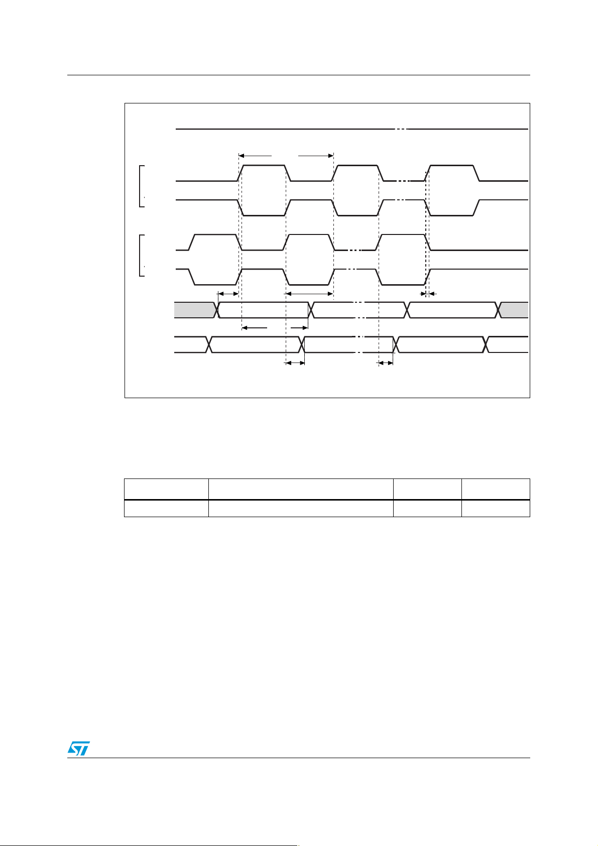
STM32F103x8, STM32F103xB Electrical characteristics
ai14136
SCK Input
CPHA=0
MOSI
OUTUT
MISO
INP UT
CPHA=0
MSBIN
M SB OUT
BIT6 IN
LSB OUT
LSB IN
CPOL=0
CPOL=1
B I T1 OUT
NSS input
t
c(SCK)
t
w(SCKH)
t
w(SCKL)
t
r(SCK)
t
f(SCK)
t
h(MI)
High
SCK Input
CPHA=1
CPHA=1
CPOL=0
CPOL=1
t
su(MI)
t
v(MO)
t
h(MO)
Figure 34. SPI timing diagram - master mode
(1)
1. Measurement points are done at CMOS levels: 0.3V
and 0.7V
DD
DD
.
USB characteristics
The USB interface is USB-IF certified (Full Speed).
Table 43. USB startup time
Symbol Parameter Max Unit
t
STARTUP
1. Guaranteed by design, not tested in production.
(1)
USB transceiver startup time 1 µs
Doc ID 13587 Rev 13 71/99

Electrical characteristics STM32F103x8, STM32F103xB
ai14137
t
f
Differen tial
data lines
V
SS
V
CR S
t
r
Crossover
points
Table 44. USB DC electrical characteristics
Symbol Parameter Conditions Min.
(1)
Input levels
V
V
CM
V
SE
USB operating voltage
DD
(4)
Differential input sensitivity I(USBDP, USBDM) 0.2
DI
(4)
Differential common mode range Includes V
(4)
Single ended receiver threshold 1.3 2.0
(2)
range 0.8 2.5
DI
3.0
(3)
Output levels
SS
(5)
(5)
2.8 3.6
V
V
1. All the voltages are measured from the local ground potential.
2. To be compliant with the USB 2.0 full-speed electrical specification, the USBDP (D+) pin should be pulled
up with a 1.5 kΩ resistor to a 3.0-to-3.6 V voltage range.
3. The STM32F103xx USB functionality is ensured down to 2.7 V but not the full USB electrical
characteristics which are degraded in the 2.7-to-3.0 V VDD voltage range.
4. Guaranteed by design, not tested in production.
R
5.
Static output level low RL of 1.5 kΩ to 3.6 V
OL
Static output level high RL of 15 kΩ to V
OH
is the load connected on the USB drivers
L
(1)
Max.
3.6 V
0.3
Unit
VV
V
Figure 35. USB timings: definition of data signal rise and fall time
Table 45. USB: Full-speed electrical characteristics
Symbol Parameter Conditions Min Max Unit
Driver characteristics
(2)
(2)
CL = 50 pF
CL = 50 pF 4 20 ns
Rise time
t
r
t
Fall time
f
t
rfm
V
CRS
1. Guaranteed by design, not tested in production.
Measured from 10% to 90% of the data signal. For more detailed informations, please refer to USB
2.
Specification - Chapter 7 (version 2.0).
Rise/ fall time matching tr/t
Output signal crossover voltage 1.3 2.0 V
(1)
f
420ns
90 110 %
5.3.17 CAN (controller area network) interface
Refer to Section 5.3.12: I/O current injection characteristics for more details on the
input/output alternate function characteristics (CAN_TX and CAN_RX).
72/99 Doc ID 13587 Rev 13
STM32F103x8, STM32F103xB Electrical characteristics
5.3.18 12-bit ADC characteristics
Unless otherwise specified, the parameters given in Ta bl e 4 6 are derived from tests
performed under the ambient temperature, f
conditions summarized in Ta bl e 9 .
Note: It is recommended to perform a calibration after each power-up.
Table 46. ADC characteristics
Symbol Parameter Conditions Min Typ Max Unit
frequency and V
PCLK2
supply voltage
DDA
V
DDA
V
REF+
I
VREF
f
ADC
f
S
f
TRIG
V
AIN
R
AIN
R
ADC
C
ADC
t
CAL
t
lat
t
latr
t
S
t
STAB
t
CONV
1. Based on characterization, not tested in production.
2. Guaranteed by design, not tested in production.
3. In devices delivered in VFQFPN and LQFP packages, V
connected to V
connected to V
4. For external triggers, a delay of 1/f
Power supply 2.4 3.6 V
Positive reference voltage 2.4 V
Current on the V
input pin 160
REF
ADC clock frequency 0.6 14 MHz
(2)
Sampling rate 0.05 1 MHz
f
= 14 MHz 823 kHz
(2)
External trigger frequency
(3)
Conversion voltage range
(2)
External input impedance
(2)
Sampling switch resistance 1 kΩ
Internal sample and hold
(2)
ADC
See Equation 1 and
Ta bl e 4 7 for details
capacitor
f
= 14 MHz 5.9 µs
(2)
Calibration time
Injection trigger conversion
(2)
ADC
= 14 MHz 0.214 µs
f
ADC
latency
= 14 MHz 0.143 µs
f
Regular trigger conversion
(2)
ADC
latency
f
= 14 MHz 0.107 17.1 µs
(2)
Sampling time
(2)
Power-up tim e 0 0 1 µs
Total conversion time
(2)
ADC
f
= 14 MHz 1 18 µs
ADC
(including sampling time)
. Devices that come in the TFBGA64 package have a V
SSA
), see Table 5 and Figure 6.
SSA
must be added to the latency specified in Table 46.
PCLK2
0 (V
SSA
tied to ground)
14 to 252 (t
successive approximation)
is internally connected to V
REF+
REF+
DDA
(1)
220
(1)
17 1/f
or V
REF-
V
REF+
50 kΩ
8pF
83 1/f
(4)
3
(4)
2
1/f
1/f
1.5 239.5 1/f
for sampling +12.5 for
S
pin but no V
DDA
and V
REF-
REF-
pin (V
is internally
is internally
REF-
1/f
V
µA
ADC
V
ADC
ADC
ADC
ADC
ADC
Doc ID 13587 Rev 13 73/99
Electrical characteristics STM32F103x8, STM32F103xB
R
AIN
T
S
f
ADCCADC
2
N2+
()ln××
------------------------------------------------------------- - R
ADC
–<
Equation 1: R
max formula:
AIN
The formula above (Equation 1) is used to determine the maximum external impedance allowed for an
error below 1/4 of LSB. Here N = 12 (from 12-bit resolution).
Table 47. R
Ts (cycles) tS (µs) R
max for f
AIN
= 14 MHz
ADC
(1)
max (kΩ)
AIN
1.5 0.11 0.4
7.5 0.54 5.9
13.5 0.96 11.4
28.5 2.04 25.2
41.5 2.96 37.2
55.5 3.96 50
71.5 5.11 NA
239.5 17.1 NA
1. Based on characterization, not tested in production.
Table 48. ADC accuracy - limited test conditions
Symbol Parameter Test conditions Typ Max
(1) (2)
(3)
Unit
ET Total unadjusted error
EO Offset error ±1 ±1.5
EG Gain error ±0.5 ±1.5
ED Differential linearity error ±0.7 ±1
EL Integral linearity error ±0.8 ±1.5
1. ADC DC accuracy values are measured after internal calibration.
2. ADC Accuracy vs. Negative Injection Current: Injecting negative current on any of the standard (nonrobust) analog input pins should be avoided as this significantly reduces the accuracy of the conversion
being performed on another analog input. It is recommended to add a Schottky diode (pin to ground) to
standard analog pins which may potentially inject negative current.
Any positive injection current within the limits specified for I
affect the ADC accuracy.
3. Based on characterization, not tested in production.
f
= 56 MHz,
PCLK2
f
= 14 MHz, R
ADC
= 3 V to 3.6 V
V
DDA
< 10 kΩ,
AIN
TA = 25 °C
Measurements made after
ADC calibration
and ΣI
INJ(PIN)
±1.3 ±2
in Section 5.3.12 does not
INJ(PIN)
LSB
74/99 Doc ID 13587 Rev 13
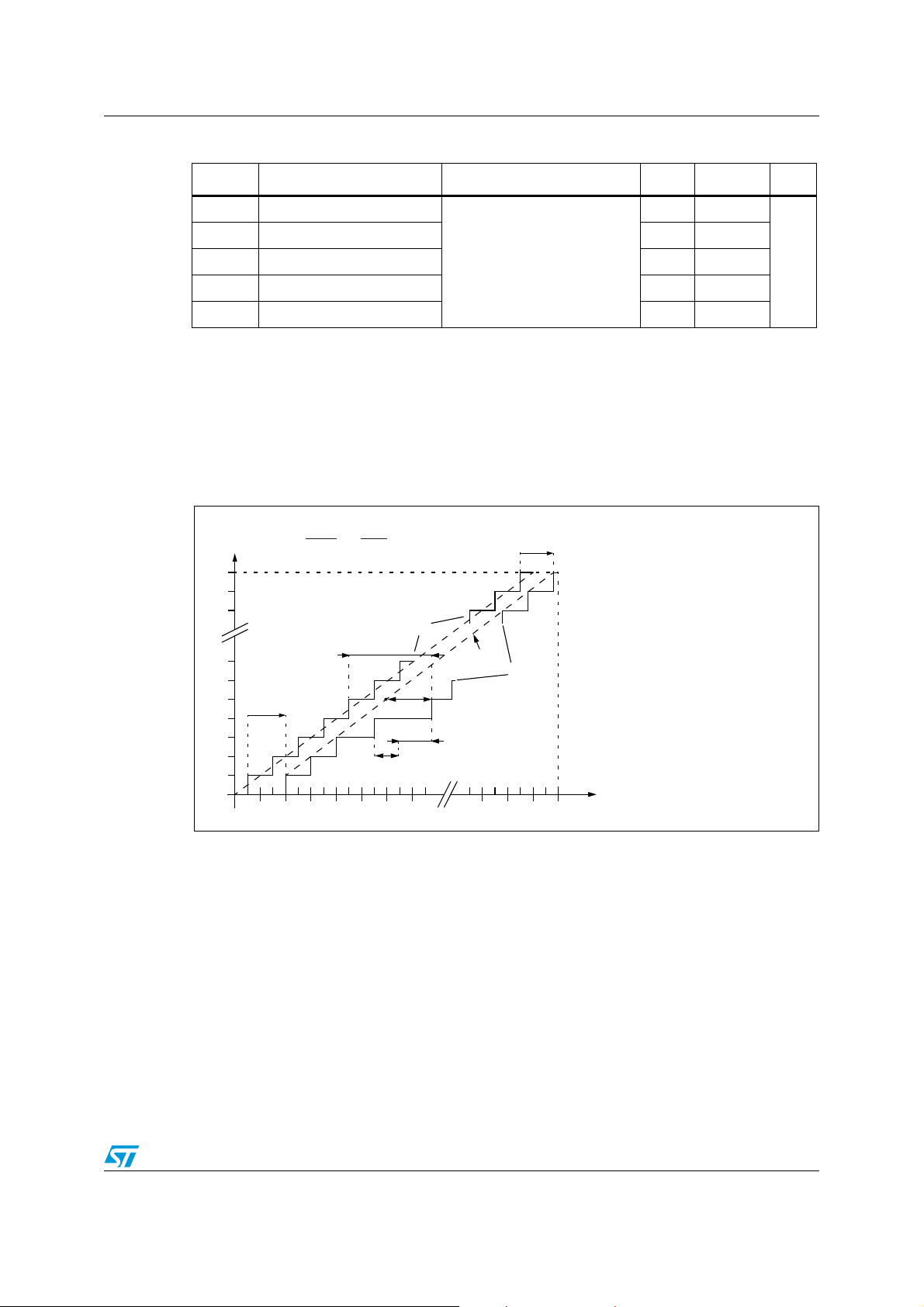
STM32F103x8, STM32F103xB Electrical characteristics
E
O
E
G
1LSB
IDEAL
(1) Example of an actual transfer curve
(2) The ideal transfer curve
(3) End point correlation line
E
T
=Total Unadjusted Error: maximum deviation
between the actual and the ideal transfer curves.
E
O
=Offset Error: deviation between the first actual
transition and the first ideal one.
E
G
=Gain Error: deviation between the last ideal
transition and the last actual one.
E
D
=Differential Linearity Error: maximum deviation
between actual steps and the ideal one.
E
L
=Integral Linearity Error: maximum deviation
between any actual transition and the end point
correlation line.
4095
4094
4093
5
4
3
2
1
0
7
6
1234567
4093 4094 4095 4096
(1)
(2)
E
T
E
D
E
L
(3)
V
DDA
V
SSA
ai14395b
V
REF+
4096
(or depending on package)]
V
DDA
4096
[1LSB
IDEAL =
Table 49. ADC accuracy
Symbol Parameter Test conditions Typ Max
ET Total unadjusted error
EO Offset error ±1.5 ±2.5
EG Gain error ±1.5 ±3
ED Differential linearity error ±1 ±2
(1) (2) (3)
f
= 56 MHz,
PCLK2
= 14 MHz, R
f
ADC
V
= 2.4 V to 3.6 V
DDA
< 10 kΩ,
AIN
Measurements made after
ADC calibration
(4)
±2 ±5
EL Integral linearity error ±1.5 ±3
1. ADC DC accuracy values are measured after internal calibration.
2. Better performance could be achieved in restricted V
3. ADC Accuracy vs. Negative Injection Current: Injecting negative current on any of the standard (nonrobust) analog input pins should be avoided as this significantly reduces the accuracy of the conversion
being performed on another analog input. It is recommended to add a Schottky diode (pin to ground) to
standard analog pins which may potentially inject negative current.
Any positive injection current within the limits specified for I
affect the ADC accuracy.
, frequency and temperature ranges.
DD
INJ(PIN)
and ΣI
in Section 5.3.12 does not
INJ(PIN)
4. Based on characterization, not tested in production.
Figure 36. ADC accuracy characteristics
Unit
LSB
Doc ID 13587 Rev 13 75/99

Electrical characteristics STM32F103x8, STM32F103xB
ai14150c
STM32F103xx
V
DD
AINx
IL±1 µA
0.6 V
V
T
R
AIN
(1)
C
parasitic
V
AIN
0.6 V
V
T
R
ADC
(1)
12-bit
converter
C
ADC
(1)
Sample and hold ADC
converter
V
REF+
(see note 1)
STM32F103xx
V
DDA
V
SSA/VREF–
(see note 1)
1 µF // 10 nF
1 µF // 10 nF
ai14388b
Figure 37. Typical connection diagram using the ADC
1. Refer to Tab l e 4 6 for the values of R
2. C
represents the capacitance of the PCB (dependent on soldering and PCB layout quality) plus the
parasitic
pad capacitance (roughly 7 pF). A high C
this, f
should be reduced.
ADC
AIN
, R
parasitic
ADC
and C
ADC
.
value will downgrade conversion accuracy. To remedy
General PCB design guidelines
Power supply decoupling should be performed as shown in Figure 38 or Figure 39,
depending on whether V
ceramic (good quality). They should be placed them as close as possible to the chip.
Figure 38. Power supply and reference decoupling (V
is connected to V
REF+
or not. The 10 nF capacitors should be
DDA
not connected to V
REF+
DDA
)
1. V
76/99 Doc ID 13587 Rev 13
and V
REF+
inputs are available only on 100-pin packages.
REF–
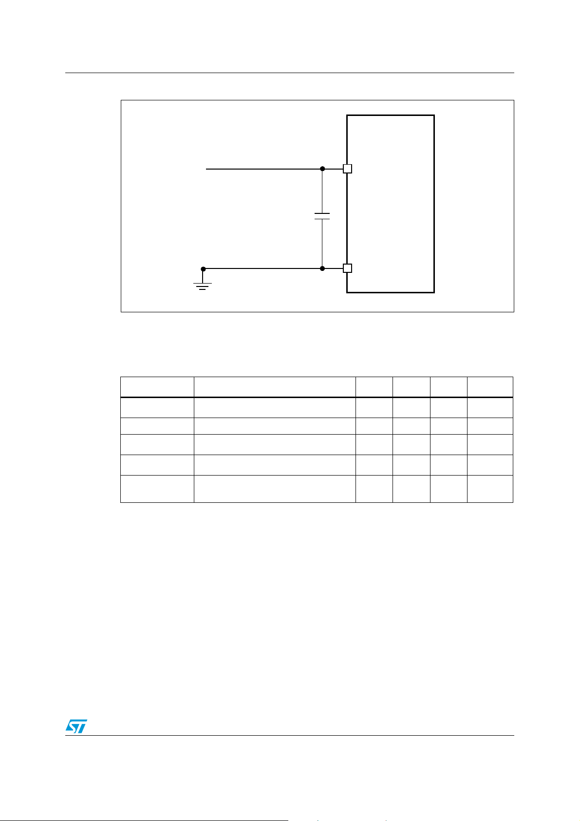
STM32F103x8, STM32F103xB Electrical characteristics
V
REF+/VDDA
STM32F103xx
1 µF // 10 nF
V
REF–/VSSA
ai14389
(See note 1)
(See note 1)
Figure 39. Power supply and reference decoupling (V
1. V
REF+
and V
inputs are available only on 100-pin packages.
REF–
5.3.19 Temperature sensor characteristics
Table 50. TS characteristics
connected to V
REF+
DDA
)
Symbol Parameter Min Typ Max Unit
(1)
T
L
Avg_Slope
(1)
V
25
(2)
t
START
S_temp
(3)(2)
T
1. Based on characterization, not tested in production.
2. Guaranteed by design, not tested in production.
3. Shortest sampling time can be determined in the application by multiple iterations.
V
linearity with temperature
SENSE
(1)
Average slope 4.0 4.3 4.6 mV/°C
±1 ±2
Voltage at 25 °C 1.34 1.43 1.52 V
Startup time 4 10 µs
ADC sampling time when reading the
temperature
17.1 µs
°C
Doc ID 13587 Rev 13 77/99

Package characteristics STM32F103x8, STM32F103xB
6 Package characteristics
6.1 Package mechanical data
In order to meet environmental requirements, ST offers these devices in different grades of
ECOPACK
specifications, grade definitions and product status are available at: www.st.com.
ECOPACK
®
packages, depending on their level of environmental compliance. ECOPACK®
®
is an ST trademark.
78/99 Doc ID 13587 Rev 13
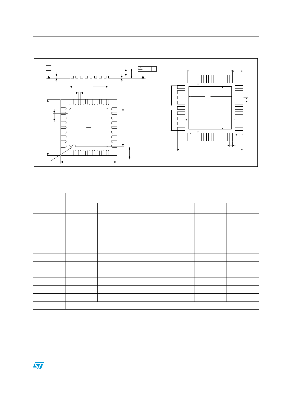
STM32F103x8, STM32F103xB Package characteristics
Seating plane
ddd C
C
A3
A1
AA2
Pin # 1 ID
R = 0.20
ZR_ME
E2
b
19
10
18
27
28
36
19
D2
E
D
e
L
0.30
6.30
0.50
1.00
4.30
4.30
4.80
4.80
4.10
4.10
1
28
9
19
ai14870b
36
27
18
10
0.75
Figure 40. VFQFPN36 6 x 6 mm, 0.5 mm pitch,
package outline
(1)
Figure 41. Recommended footprint
(dimensions in mm)
1. Drawing is not to scale.
2. All leads/pads should also be soldered to the PCB to improve the lead solder joint life.
Table 51. VFQFPN36 6 x 6 mm, 0.5 mm pitch, package mechanical data
millimeters inches
Symbol
Min Typ Max Min Typ Max
(1)(2)
(1)
A 0.800 0.900 1.000 0.0315 0.0354 0.0394
A1 0.020 0.050 0.0008 0.0020
A2 0.650 1.000 0.0256 0.0394
A3 0.250 0.0098
b 0.180 0.230 0.300 0.0071 0.0091 0.0118
D 5.875 6.000 6.125 0.2313 0.2362 0.2411
D2 1.750 3.700 4.250 0.0689 0.1457 0.1673
E 5.875 6.000 6.125 0.2313 0.2362 0.2411
E2 1.750 3.700 4.250 0.0689 0.1457 0.1673
e 0.450 0.500 0.550 0.0177 0.0197 0.0217
L 0.350 0.550 0.750 0.0138 0.0217 0.0295
ddd 0.080 0.0031
1. Values in inches are converted from mm and rounded to 4 decimal digits.
Doc ID 13587 Rev 13 79/99
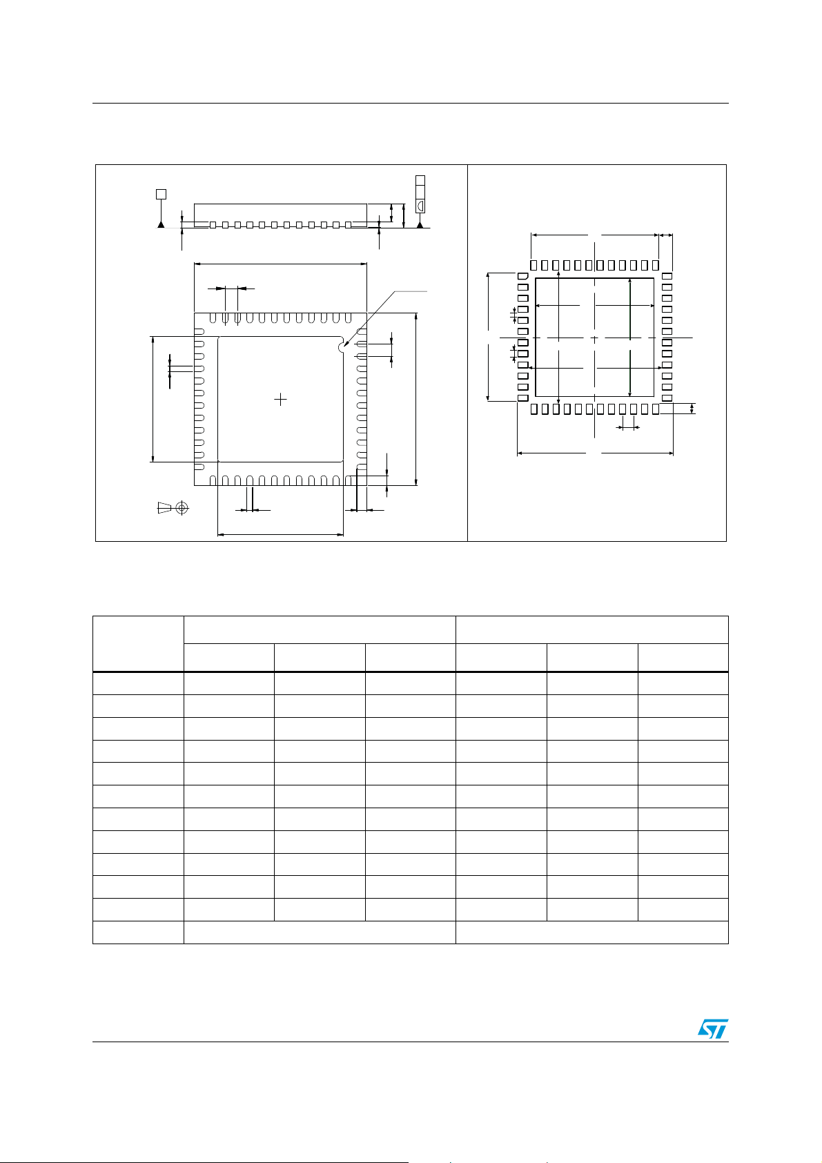
Package characteristics STM32F103x8, STM32F103xB
Seating
Plane
C
A3
A1
A2
A
ddd C
Pin no. 1 ID
R = 0.20
Bottom View
1
48
e
E
L
L
12
13
D2
b
24
25
b
E2
36
37
e
D
V0_ME
0.50
7.30
0.75
5.80
5.80
6.20
6.20
5.60
5.60
13
1
24
37
ai15799
12
48
36
25
0.55
0.30
0.20
Figure 42. VFQFPN48 7 x 7 mm, 0.5 mm pitch, package
outline
(1)
Figure 43. Recommended footprint
(dimensions in mm)
(1)(2)
1. Drawing is not to scale.
2. All leads/pads should also be soldered to the PCB to improve the lead solder joint life.
Table 52. VFQFPN48 7 x 7 mm, 0.5 mm pitch, package mechanical data
millimeters inches
(1)
Symbol
Min Typ Max Min Typ Max
A 0.800 0.900 1.000 0.0315 0.0354 0.0394
A1 0.020 0.050 0.0008 0.0020
A2 0.650 1.000 0.0256 0.0394
A3 0.250 0.0098
b 0.180 0.230 0.300 0.0071 0.0091 0.0118
D 6.850 7.000 7.150 0.2697 0.2756 0.2815
D2 2.250 4.700 5.250 0.0886 0.1850 0.2067
E 6.850 7.000 7.150 0.2697 0.2756 0.2815
E2 2.250 4.700 5.250 0.0886 0.1850 0.2067
e 0.450 0.500 0.550 0.0177 0.0197 0.0217
L 0.300 0.400 0.500 0.0118 0.0157 0.0197
ddd 0.080 0.0031
1. Values in inches are converted from mm and rounded to 4 decimal digits.
80/99 Doc ID 13587 Rev 13

STM32F103x8, STM32F103xB Package characteristics
Figure 44. LFBGA100 - 10 x 10 mm low profile fine pitch ball grid array package
outline
1. Drawing is not to scale.
Table 53. LFBGA100 - 10 x 10 mm low profile fine pitch ball grid array package
mechanical data
millimeters inches
Symbol
Min Typ Max Min Typ Max
A 1.700 0.0669
A1 0.270 0.0106
A2 1.085 0.0427
A3 0.30 0.0118
A4 0.80 0.0315
b 0.45 0.50 0.55 0.0177 0.0197 0.0217
D 9.85 10.00 10.15 0.3878 0.3937 0.3996
D1 7.20 0.2835
E 9.85 10.00 10.15 0.3878 0.3937 0.3996
E1 7.20 0.2835
e 0.80 0.0315
F 1.40 0.0551
ddd 0.12 0.0047
eee 0.15 0.0059
fff 0.08 0.0031
N (number of balls) 100
1. Values in inches are converted from mm and rounded to 4 decimal digits.
(1)
Doc ID 13587 Rev 13 81/99

Package characteristics STM32F103x8, STM32F103xB
Dpad
Dsm
Dpad 0.37 mm
Dsm
0.52 mm typ. (depends on solder
mask registration tolerance
Solder paste 0.37 mm aperture diameter
– Non solder mask defined pads are recommended
– 4 to 6 mils screen print
Figure 45. Recommended PCB design rules (0.80/0.75 mm pitch BGA)
82/99 Doc ID 13587 Rev 13

STM32F103x8, STM32F103xB Package characteristics
D
D1
D3
75
51
50
76
100 26
125
E3 E1 E
e
b
Pin 1
identification
SEATING PLANE
GAGE PLANE
C
A
A2
A1
Cccc
0.25 mm
0.10 inch
L
L1
k
C
1L_ME
75 51
5076
0.5
0.3
16.7 14.3
100 26
12.3
25
1.2
16.7
1
ai14906
Figure 46. LQFP100, 14 x 14 mm 100-pin low-profile
quad flat package outline
(1)
Figure 47. Recommended footprint
1. Drawing is not to scale.
2. Dimensions are in millimeters.
Table 54. LQPF100, 14 x 14 mm 100-pin low-profile quad flat package mechanical data
millimeters inches
(1)
Symbol
Min Typ Max Min Typ Max
(1)(2)
1. Values in inches are converted from mm and rounded to 4 decimal digits.
A 1.6 0.063
A1 0.05 0.15 0.002 0.0059
A2 1.35 1.4 1.45 0.0531 0.0551 0.0571
b 0.17 0.22 0.27 0.0067 0.0087 0.0106
c 0.09 0.2 0.0035 0.0079
D 15.8 16 16.2 0.622 0.6299 0.6378
D1 13.8 14 14.2 0.5433 0.5512 0.5591
D3 12 0.4724
E 15.8 16 16.2 0.622 0.6299 0.6378
E1 13.8 14 14.2 0.5433 0.5512 0.5591
E3 12 0.4724
e 0.5 0.0197
L 0.45 0.6 0.75 0.0177 0.0236 0.0295
L1 1 0.0394
k 0.0° 3.5° 7.0° 0.0° 3.5° 7.0°
ccc 0.08 0.0031
Doc ID 13587 Rev 13 83/99

Package characteristics STM32F103x8, STM32F103xB
A
A2
A1
c
L1
L
E
E1
D
D1
e
b
ai14398b
48
3249
64 17
116
1.2
0.3
33
10.3
12.7
10.3
0.5
7.8
12.7
ai14909
Figure 48. LQFP64, 10 x 10 mm, 64-pin low-profile quad
flat package outline
(1)
Figure 49. Recommended
footprint
(1)(2)
1. Drawing is not to scale.
2. Dimensions are in millimeters.
Table 55. LQFP64, 10 x 10 mm, 64-pin low-profile quad flat package mechanical data
millimeters inches
(1)
Symbol
Min Typ Max Min Typ Max
A 1.60 0.0630
A1 0.05 0.15 0.0020 0.0059
A2 1.35 1.40 1.45 0.0531 0.0551 0.0571
b 0.17 0.22 0.27 0.0067 0.0087 0.0106
c 0.09 0.20 0.0035 0.0079
D 12.00 0.4724
D1 10.00 0.3937
E 12.00 0.4724
E1 10.00 0.3937
e 0.50 0.0197
θ 0° 3.5° 7° 0° 3.5° 7°
L 0.45 0.60 0.75 0.0177 0.0236 0.0295
L1 1.00 0.0394
Number of pins
N
64
1. Values in inches are converted from mm and rounded to 4 decimal digits.
84/99 Doc ID 13587 Rev 13
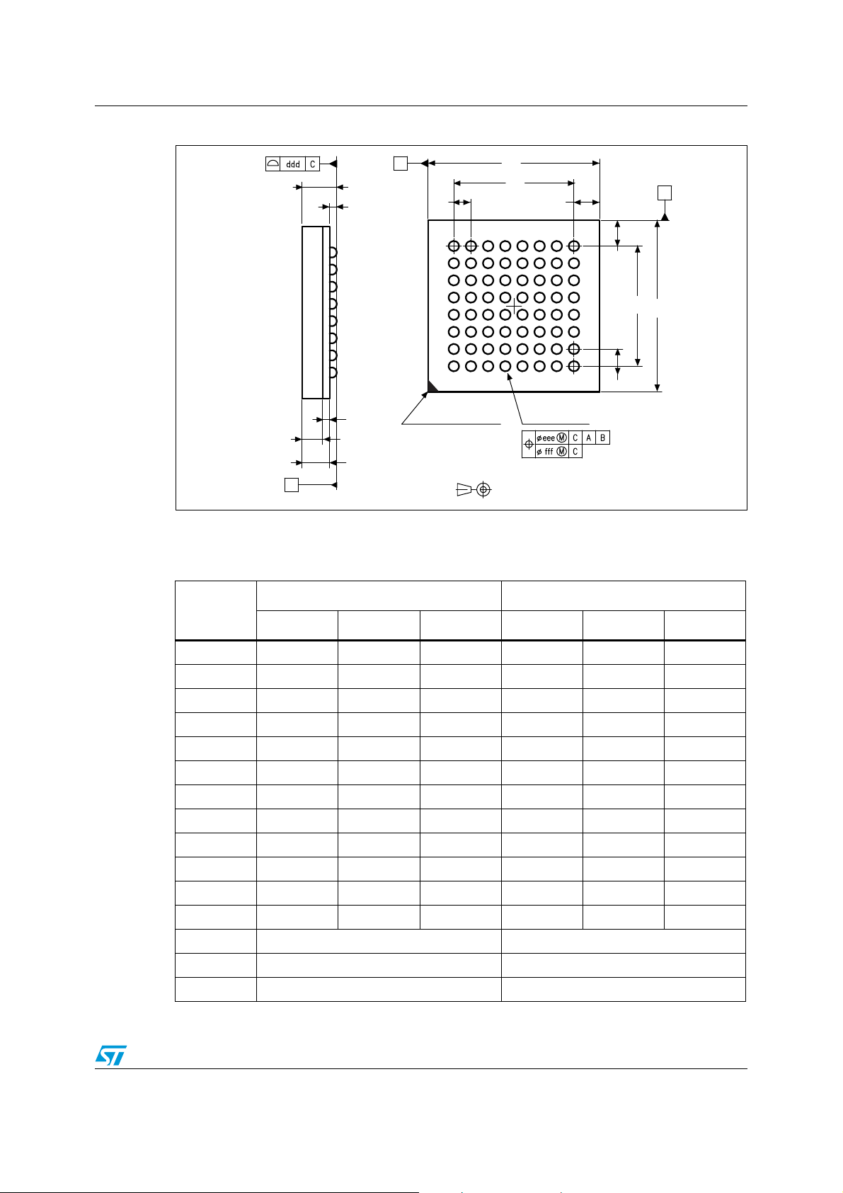
STM32F103x8, STM32F103xB Package characteristics
A3
A4
A2
A1
A
Seating
plane
B
A
D
D1
e
F
F
E1 E
e
H
G
F
E
D
C
B
A
123 45678
A1 ball pad corner
Øb (64 balls)
Bottom view
C
ME_R8
Figure 50. TFBGA64 - 8 x 8 active ball array, 5 x 5 mm, 0.5 mm pitch, package outline
1. Drawing is not to scale.
Table 56. TFBGA64 - 8 x 8 active ball array, 5 x 5 mm, 0.5 mm pitch, package
mechanical data
millimeters inches
Symbol
Min Typ Max Min Typ Max
A 1.200 0.0472
A1 0.150 0.0059
A2 0.785 0.0309
A3 0.200 0.0079
A4 0.600 0.0236
b 0.250 0.300 0.350 0.0098 0.0118 0.0138
D 4.850 5.000 5.150 0.1909 0.1969 0.2028
D1 3.500 0.1378
E 4.850 5.000 5.150 0.1909 0.1969 0.2028
E1 3.500 0.1378
e 0.500 0.0197
F 0.750 0.0295
ddd 0.080 0.0031
eee 0.150 0.0059
fff 0.050 0.0020
1. Values in inches are converted from mm and rounded to 4 decimal digits.
Doc ID 13587 Rev 13 85/99
(1)

Package characteristics STM32F103x8, STM32F103xB
Figure 51. Recommended PCB design rules for pads (0.5 mm pitch BGA)
Dpad
Dsm
1. Non solder mask defined (NSMD) pads are recommended
2. 4 to 6 mils solder paste screen printing process
Pitch
D pad 0.27 mm
Dsm
Solder paste
0.5 mm
0.35 mm typ (depends on
the soldermask registration
tolerance)
0.27 mm aperture diameter
ai15495
86/99 Doc ID 13587 Rev 13

STM32F103x8, STM32F103xB Package characteristics
D
D1
D3
A1
L1
L
k
c
b
ccc
C
A1
A2A
C
Seating plane
0.25 mm
Gage plane
E3
E1
E
12
13
24
25
48
1
36
37
Pin 1
identification
5B_ME
9.70
5.80
7.30
12
24
0.20
7.30
1
37
36
1.20
5.80
9.70
0.30
25
1.20
0.50
ai14911b
1348
Figure 52. LQFP48, 7 x 7 mm, 48-pin low-profile quad flat
package outline
(1)
Figure 53. Recommended
footprint
1. Drawing is not to scale.
2. Dimensions are in millimeters.
Table 57. LQFP48, 7 x 7 mm, 48-pin low-profile quad flat package mechanical data
millimeters inches
(1)
Symbol
Min Typ Max Min Typ Max
(1)(2)
A 1.600 0.0630
A1 0.050 0.150 0.0020 0.0059
A2 1.350 1.400 1.450 0.0531 0.0551 0.0571
b 0.170 0.220 0.270 0.0067 0.0087 0.0106
c 0.090 0.200 0.0035 0.0079
D 8.800 9.000 9.200 0.3465 0.3543 0.3622
D1 6.800 7.000 7.200 0.2677 0.2756 0.2835
D3 5.500 0.2165
E 8.800 9.000 9.200 0.3465 0.3543 0.3622
E1 6.800 7.000 7.200 0.2677 0.2756 0.2835
E3 5.500 0.2165
e 0.500 0.0197
1. Values in inches are converted from mm and rounded to 4 decimal digits.
L 0.450 0.600 0.750 0.0177 0.0236 0.0295
L1 1.000 0.0394
k 0°3.5°7° 0°3.5°7°
ccc 0.080 0.0031
Doc ID 13587 Rev 13 87/99
Package characteristics STM32F103x8, STM32F103xB
6.2 Thermal characteristics
The maximum chip junction temperature (TJmax) must never exceed the values given in
Table 9: General operating conditions on page 36.
The maximum chip-junction temperature, T
max, in degrees Celsius, may be calculated
J
using the following equation:
T
max = TA max + (PD max × ΘJA)
J
Where:
● T
● Θ
● P
● P
max is the maximum ambient temperature in °C,
A
is the package junction-to-ambient thermal resistance, in °C/W,
JA
max is the sum of P
D
max is the product of I
INT
max and P
INT
DD
max (PD max = P
I/O
INT
and VDD, expressed in Watts. This is the maximum chip
max + P
I/O
max),
internal power.
P
max represents the maximum power dissipation on output pins where:
I/O
P
max = Σ (VOL × IOL) + Σ((V
I/O
taking into account the actual V
OL
– VOH) × IOH),
DD
/ IOL and VOH / I
of the I/Os at low and high level in the
OH
application.
Table 58. Package thermal characteristics
Symbol Parameter Value Unit
Thermal resistance junction-ambient
LFBGA100 - 10 × 10 mm / 0.8 mm pitch
Thermal resistance junction-ambient
LQFP100 - 14 × 14 mm / 0.5 mm pitch
44
46
Thermal resistance junction-ambient
LQFP64 - 10 × 10 mm / 0.5 mm pitch
Θ
Thermal resistance junction-ambient
JA
TFBGA64 - 5 × 5 mm / 0.5 mm pitch
Thermal resistance junction-ambient
LQFP48 - 7 x 7 mm / 0.5 mm pitch
Thermal resistance junction-ambient
VFQFPN 48 -7 × 7 mm / 0.5 mm pitch
Thermal resistance junction-ambient
VFQFPN 36 - 6 × 6 mm / 0.5 mm pitch
6.2.1 Reference document
JESD51-2 Integrated Circuits Thermal Test Method Environment Conditions - Natural
Convection (Still Air). Available from www.jedec.org.
45
65
55
16
18
°C/W
88/99 Doc ID 13587 Rev 13

STM32F103x8, STM32F103xB Package characteristics
6.2.2 Selecting the product temperature range
When ordering the microcontroller, the temperature range is specified in the ordering
information scheme shown in Table 59: Ordering information scheme.
Each temperature range suffix corresponds to a specific guaranteed ambient temperature at
maximum dissipation and, to a specific maximum junction temperature.
As applications do not commonly use the STM32F103xx at maximum dissipation, it is useful
to calculate the exact power consumption and junction temperature to determine which
temperature range will be best suited to the application.
The following examples show how to calculate the temperature range needed for a given
application.
Example 1: High-performance application
Assuming the following application conditions:
Maximum ambient temperature T
I
= 50 mA, VDD = 3.5 V, maximum 20 I/Os used at the same time in output at low
DDmax
level with I
at low level with I
P
INTmax =
P
IOmax =
This gives: P
P
Dmax =
Thus: P
Dmax
= 8 mA, VOL= 0.4 V and maximum 8 I/Os used at the same time in output
OL
= 20 mA, VOL= 1.3 V
OL
50 mA × 3.5 V= 175 mW
20 × 8 mA × 0.4 V + 8 × 20 mA × 1.3 V = 272 mW
= 175 mW and P
INTmax
175 + 272 = 447 mW
= 447 mW
Using the values obtained in Tab le 5 8 T
– For LQFP100, 46 °C/W
T
= 82 °C + (46 °C/W × 447 mW) = 82 °C + 20.6 °C = 102.6 °C
Jmax
This is within the range of the suffix 6 version parts (–40 < T
In this case, parts must be ordered at least with the temperature range suffix 6 (see
Table 59: Ordering information scheme).
= 82 °C (measured according to JESD51-2),
Amax
= 272 mW:
IOmax
is calculated as follows:
Jmax
< 105 °C).
J
Example 2: High-temperature application
Using the same rules, it is possible to address applications that run at high ambient
temperatures with a low dissipation, as long as junction temperature T
specified range.
Assuming the following application conditions:
Maximum ambient temperature T
I
= 20 mA, VDD = 3.5 V, maximum 20 I/Os used at the same time in output at low
DDmax
level with I
P
INTmax =
P
IOmax =
This gives: P
P
Dmax = 70 +
Thus: P
Dmax
= 8 mA, VOL= 0.4 V
OL
20 mA × 3.5 V= 70 mW
20 × 8 mA × 0.4 V = 64 mW
= 70 mW and P
INTmax
64 = 134 mW
= 134 mW
Doc ID 13587 Rev 13 89/99
= 115 °C (measured according to JESD51-2),
Amax
= 64 mW:
IOmax
remains within the
J
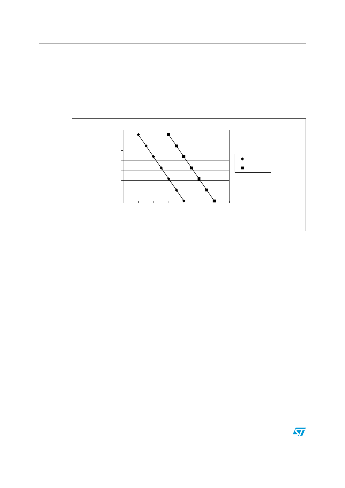
Package characteristics STM32F103x8, STM32F103xB
0
100
200
300
400
500
600
700
65 75 85 95 105 115 125 135
TA (°C)
P
D
(mW)
Suffix 6
Suffix 7
Using the values obtained in Tab le 5 8 T
is calculated as follows:
Jmax
– For LQFP100, 46 °C/W
T
= 115 °C + (46 °C/W × 134 mW) = 115 °C + 6.2 °C = 121.2 °C
Jmax
This is within the range of the suffix 7 version parts (–40 < T
< 125 °C).
J
In this case, parts must be ordered at least with the temperature range suffix 7 (see
Table 59: Ordering information scheme).
Figure 54. LQFP100 P
max vs. T
D
A
90/99 Doc ID 13587 Rev 13

STM32F103x8, STM32F103xB Ordering information scheme
7 Ordering information scheme
Table 59. Ordering information scheme
Example: STM32 F 103 C 8 T 7 xxx
Device family
STM32 = ARM-based 32-bit microcontroller
Product type
F = general-purpose
Device subfamily
103 = performance line
Pin count
T = 36 pins
C = 48 pins
R = 64 pins
V = 100 pins
Flash memory size
(1)
8 = 64 Kbytes of Flash memory
B = 128 Kbytes of Flash memory
Package
H = BGA
T = LQFP
U = VFQFPN
Temperature range
6 = Industrial temperature range, –40 to 85 °C.
7 = Industrial temperature range, –40 to 105 °C.
Options
xxx = programmed parts
TR = tape and real
1. Although STM32F103x6 devices are not described in this datasheet, orderable part numbers that do not
show the A internal code after temperature range code 6 or 7 should be referred to this datasheet for the
electrical characteristics. The low-density datasheet only covers STM32F103x6 devices that feature the
A code.
For a list of available options (speed, package, etc.) or for further information on any aspect
of this device, please contact your nearest ST sales office.
Doc ID 13587 Rev 13 91/99

Revision history STM32F103x8, STM32F103xB
8 Revision history
Table 60. Document revision history
Date Revision Changes
01-jun-2007 1 Initial release.
Flash memory size modified in Note 8, Note 5, Note 7, Note 9 and
BGA100 pins added to Table 5: Medium-density STM32F103xx pin
definitions. Figure 3: STM32F103xx performance line LFBGA100
ballout added.
20-Jul-2007 2
changed to T
T
HSE
AC timing diagram. V
t
SU(LSE)
changed to t
characteristics. I
characteristics.
Sample size modified and machine model removed in Electrostatic
discharge (ESD).
Number of parts modified and standard reference updated in Static
latch-up. 25 °C and 85 °C conditions removed and class name modified
in Table 33: Electrical sensitivities. R
added to Table 35: I/O static characteristics. RPU min and max values
added to Table 38: NRST pin characteristics.
Figure 31: I2C bus AC waveforms and measurement circuit and
Figure 30: Recommended NRST pin protection corrected.
Notes removed below Ta bl e 9 , Ta bl e 3 8 , Tab l e 4 4.
typical values changed in Table 11: Maximum current consumption
I
DD
in Run and Sleep modes. Table 39: TIMx characteristics modified.
, V
t
STAB
REF+
value, t
characteristics.
In Table 29: Flash memory endurance and data retention, typical
endurance and data retention for T
TA = 25 °C removed.
changed to V
V
BG
voltage. Document title changed. Controller area network (CAN)
section modified.
Figure 13: Power supply scheme modified.
Features on page 1 list optimized. Small text changes.
in Figure 22: Low-speed external clock source
LSE
ranged modified in Power supply schemes.
BAT
in Table 22: HSE 4-16 MHz oscillator
SU(HSE)
max value added to Table 24: HSI oscillator
DD(HSI)
and RPD min and max values
PU
and f
lat
REFINT
added to Table 46: ADC
TRIG
= 85 °C added, data retention for
A
in Table 12: Embedded internal reference
92/99 Doc ID 13587 Rev 13
STM32F103x8, STM32F103xB Revision history
Table 60. Document revision history (continued)
Date Revision Changes
STM32F103CBT6, STM32F103T6 and STM32F103T8 root part
numbers added (see Table 2: STM32F103xx medium-density device
features and peripheral counts)
VFQFPN36 package added (see Section 6: Package characteristics).
All packages are ECOPACK® compliant. Package mechanical data
inch values are calculated from mm and rounded to 4 decimal digits
(see Section 6: Package characteristics).
Table 5: Medium-density STM32F103xx pin definitions updated and
clarified.
Table 26: Low-power mode wakeup timings updated.
min corrected in Table 12: Embedded internal reference voltage.
T
A
Note 2 added below Table 22: HSE 4-16 MHz oscillator characteristics.
value added to Table 32: ESD absolute maximum ratings.
parameter description modified in Table 36:
OH
, tS max, t
added in Table 46: ADC characteristics.
latr
hys
values updated in Table 24: HSI oscillator characteristics.
HSI
, V
CONV
REF+
min and t
max modified, notes modified
lat
modified in Table 35: I/O static characteristics.
modified in Table 10: Operating
VDD
value added in Ta bl e 3 0 :
FESD
DD/VBAT
= 2.4 V, Note 2
added to Table 28: Flash memory characteristics.
value added in Table 25: LSI oscillator characteristics and
LSI
added to Table 50: TS characteristics. N
modified in
END
added to Table 12: Embedded internal reference voltage.
and f
removed from Table 27: PLL characteristics.
VCO
18-Oct-2007 3
V
ESD(CDM)
Note 4 added and V
Output voltage characteristics.
Note 1 modified under Table 37: I/O AC characteristics.
Equation 1 and Table 47: RAIN max for fADC = 14 MHz added to
Section 5.3.18: 12-bit ADC characteristics.
V
AIN
and t
Figure 36: ADC accuracy characteristics updated. Note 1 modified
below Figure 37: Typical connection diagram using the ADC.
Electrostatic discharge (ESD) on page 58 modified.
Number of TIM4 channels modified in Figure 1: STM32F103xx
performance line block diagram.
Maximum current consumption Ta bl e 1 3 , Tab l e 1 4 and Ta b le 1 5
updated. V
Table 49: ADC accuracy updated. t
conditions at power-up / power-down. V
EMS characteristics.
Values corrected, note 2 modified and note 3 removed in Tab le 2 6:
Low-power mode wakeup timings.
Table 16: Typical and maximum current consumptions in Stop and
Standby modes: Typical values added for V
modified, Note 2 added.
Table 21: Typical current consumption in Standby mode added. On-chip
peripheral current consumption on page 48 added.
ACC
V
prog
Upper option byte address modified in Figure 10: Memory map.
Typical f
internal RC value corrected from 32 to 40 kHz in entire document.
T
S_temp
Table 29: Flash memory endurance and data retention.
T
S_vrefint
Handling of unused pins specified in General input/output
characteristics on page 60. All I/Os are CMOS and TTL compliant.
Figure 38: Power supply and reference decoupling (VREF+ not
connected to VDDA) modified.
t
JITTER
Appendix A: Important notes on page 81 added.
Added Figure 15, Figure 16, Figure 18 and Figure 20.
Doc ID 13587 Rev 13 93/99

Revision history STM32F103x8, STM32F103xB
Table 60. Document revision history (continued)
Date Revision Changes
Document status promoted from preliminary data to datasheet.
The STM32F103xx is USB certified. Small text changes.
Power supply schemes on page 15 modified. Number of
communication peripherals corrected for STM32F103Tx and number of
GPIOs corrected for LQFP package in Table 2: STM32F103xx medium-
density device features and peripheral counts.
Main function and default alternate function modified for PC14 and
PC15 in, Note 6 added and Remap column added in Table 5: Medium-
density STM32F103xx pin definitions.
ratings and Note 1 modified in Table 6: Voltage
modified in Table 7: Current characteristics.
value at 72 MHz with peripherals enabled modified in Ta bl e 1 4 :
value at 72 MHz with peripherals enabled modified in Ta bl e 1 5 :
typical value at 2.4 V modified and I
and t
conditions modified in Table 29: Flash memory endurance
RET
, t
AIN
conditions modified in Ta b le 2 2 and Ta bl e 2 3 ,
SU(LSE)
lat and tlatr
modified, note added and I
DD_VBAT
maximum values
removed in
lkg
value for VFQFPN36 package added in Table 58: Package thermal
modified in Ta b l e 5 0: T S
25
22-Nov-2007 4
V
DD–VSS
characteristics, Note 1
Note 1 and Note 2 added in Table 11: Embedded reset and power
control block characteristics.
I
DD
Maximum current consumption in Run mode, code with data
processing running from RAM.
I
DD
Maximum current consumption in Sleep mode, code running from
Flash or RAM on page 42.
I
DD_VBAT
added in Table 16: Typical and maximum current consumptions in Stop
and Standby modes. Note added in Table 17 on page 46 and Table 18
on page 47. ADC1 and ADC2 consumption and notes modified in
Table 19: Peripheral current consumption.
t
SU(HSE)
respectively.
Maximum values removed from Table 26: Low-power mode wakeup
timings. t
and data retention. Figure 13: Power supply scheme corrected.
Figure 19: Typical current consumption in Stop mode with regulator in
Low-power mode versus temperature at VDD = 3.3 V and 3.6 V added.
Note removed below Figure 32: SPI timing diagram - slave mode and
CPHA = 0. Note added below Figure 33: SPI timing diagram - slave
mode and CPHA = 1(1).
Details on unused pins removed from General input/output
characteristics on page 60.
Table 42: SPI characteristics updated. Table 43: USB startup time
added. V
Table 46: ADC characteristics. Test conditions modified and note added
in Table 49: ADC accuracy. Note added below Ta b le 4 7 and Tab l e 5 0 .
Inch values corrected in Table 54: LQPF100, 14 x 14 mm 100-pin low-
profile quad flat package mechanical data, Table 55: LQFP64, 10 x 10
mm, 64-pin low-profile quad flat package mechanical data and
Table 57: LQFP48, 7 x 7 mm, 48-pin low-profile quad flat package
mechanical data.
Θ
JA
characteristics.
Order codes replaced by Section 7: Ordering information scheme.
MCU ‘s operating conditions modified in Typical current consumption
on page 45. Avg_Slope and V
characteristics. I2C interface characteristics on page 67 modified.
Impedance size specified in A.4: Voltage glitch on ADC input 0 on
page 81.
94/99 Doc ID 13587 Rev 13
STM32F103x8, STM32F103xB Revision history
Table 60. Document revision history (continued)
Date Revision Changes
Figure 2: Clock tree on page 12 added.
value given in Table 8: Thermal characteristics on
J
modified in Table 24: HSI oscillator characteristics on page 53,
values modified and t
prog
description clarified
prog
unit corrected in Table 38: NRST pin characteristics on
added to Table 46: ADC characteristics on page 73.
14-Mar-2008 5
Maximum T
page 36.
CRC feature added (see CRC (cyclic redundancy check) calculation
unit on page 9 and Figure 10: Memory map on page 32 for address).
modified in Table 16: Typical and maximum current consumptions in
I
DD
Stop and Standby modes.
ACC
HSI
note 2 removed.
, TA and TJ added, t
P
D
in Table 28: Flash memory characteristics on page 55.
modified in Table 29: Flash memory endurance and data retention.
t
RET
V
NF(NRST)
page 65.
Table 42: SPI characteristics on page 69 modified.
I
VREF
Table 48: ADC accuracy - limited test conditions added. Table 49: ADC
accuracy modified.
LQFP100 package specifications updated (see Section 6: Package
characteristics on page 78).
Recommended LQFP100, LQFP 64, LQFP48 and VFQFPN36
footprints added (see Figure 47, Figure 49, Figure 53 and Figure 41).
Section 6.2: Thermal characteristics on page 88 modified,
Section 6.2.1 and Section 6.2.2 added.
Appendix A: Important notes on page 81 removed.
21-Mar-2008 6
22-May-2008 7
Small text changes. Figure 10: Memory map clarified.
In Table 29: Flash memory endurance and data retention:
tested over the whole temperature range
–N
END
– cycling conditions specified for t
–t
min modified at TA = 55 °C
RET
, Avg_Slope and TL modified in Table 50: TS characteristics.
V
25
RET
CRC feature removed.
CRC feature added back. Small text changes. Section 1: Introduction
modified. Section 2.2: Full compatibility throughout the family added.
at TA max = 105 °C added to Table 16: Typical and maximum
I
DD
current consumptions in Stop and Standby modes on page 43.
I
DD_VBAT
removed from Table 21: Typical current consumption in
Standby mode on page 47.
Values added to Table 41: SCL frequency (fPCLK1= 36 MHz.,VDD =
3.3 V) on page 68.
Figure 32: SPI timing diagram - slave mode and CPHA = 0 on page 70
modified. Equation 1 corrected.
at TA = 105 °C modified in Table 29: Flash memory endurance and
t
RET
data retention on page 56.
added to Table 44: USB DC electrical characteristics on page 72.
V
USB
Figure 54: LQFP100 PD max vs. TA on page 90 modified.
Axx option added to Table 59: Ordering information scheme on
page 91.
Doc ID 13587 Rev 13 95/99
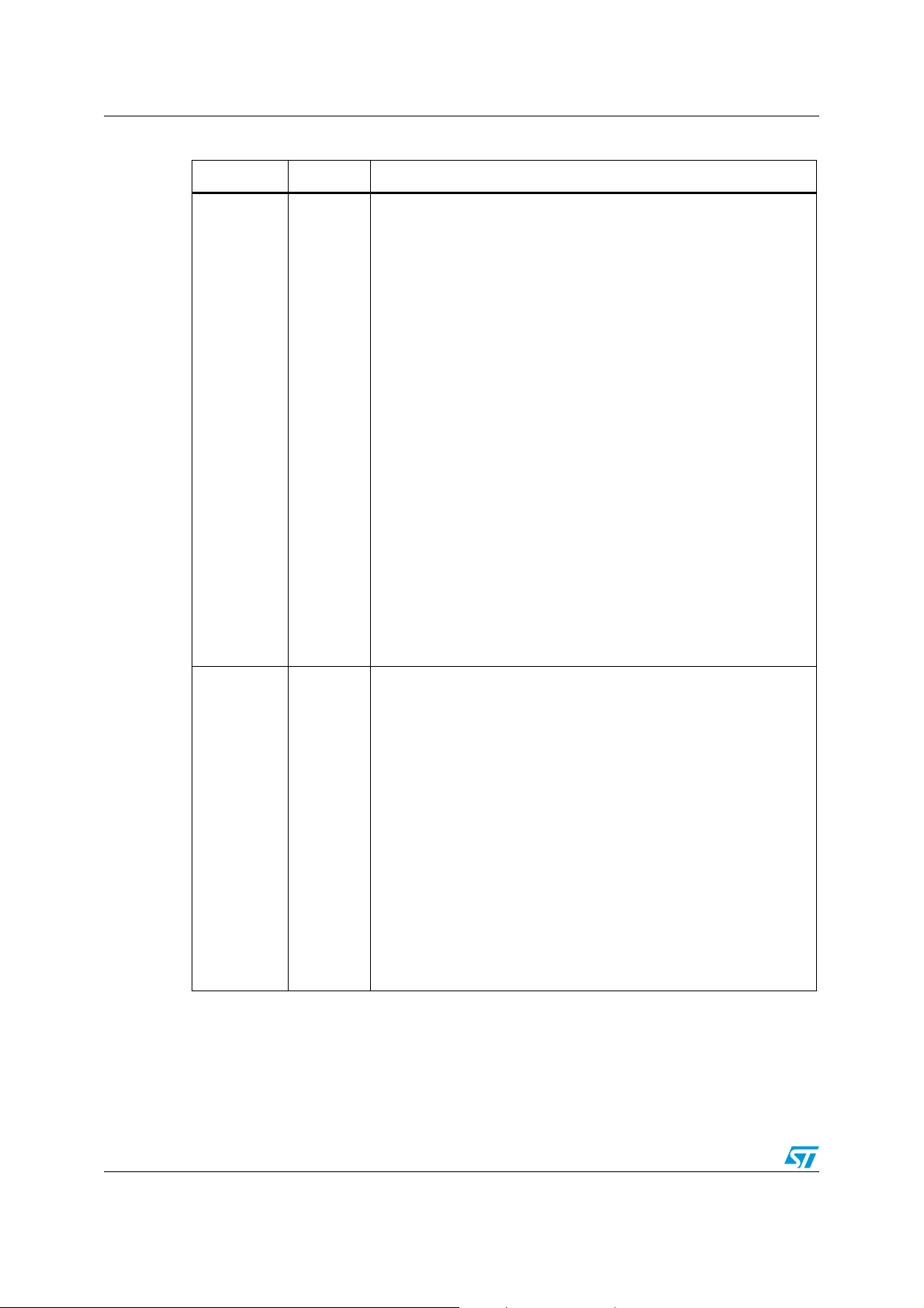
Revision history STM32F103x8, STM32F103xB
Table 60. Document revision history (continued)
Date Revision Changes
21-Jul-2008 8
22-Sep-2008 9
Power supply supervisor updated and V
added to Ta b l e 9 : G en er a l
DDA
operating conditions.
Capacitance modified in Figure 13: Power supply scheme on page 34.
Table notes revised in Section 5: Electrical characteristics.
Table 16: Typical and maximum current consumptions in Stop and
Standby modes modified.
Data added to Table 16: Typical and maximum current consumptions in
Stop and Standby modes and Table 21: Typical current consumption in
Standby mode removed.
f
characteristics on page 49. f
modified in Table 20: High-speed external user clock
HSE_ext
modified in Table 27: PLL
PLL_IN
characteristics on page 55.
Minimum SDA and SCL fall time value for Fast mode removed from
Table 40: I2C characteristics on page 67, note 1 modified.
modified in Table 42: SPI characteristics on page 69 and
t
h(NSS)
Figure 32: SPI timing diagram - slave mode and CPHA = 0 on page 70.
modified in Table 46: ADC characteristics on page 73 and
C
ADC
Figure 37: Typical connection diagram using the ADC modified.
Typical T
value removed from Table 50: TS characteristics on
S_temp
page 77.
LQFP48 package specifications updated (see Ta bl e 5 7 and Ta bl e 5 3 ),
Section 6: Package characteristics revised.
Axx option removed from Table 59: Ordering information scheme on
page 91.
Small text changes.
STM32F103x6 part numbers removed (see Table 59: Ordering
information scheme). Small text changes.
General-purpose timers (TIMx) and Advanced-control timer (TIM1) on
page 18 updated.
Notes updated in Table 5: Medium-density STM32F103xx pin
definitions on page 27.
Note 2 modified below Table 6: Voltage characteristics on page 35,
|ΔV
DDx
| min and |ΔV
| min removed.
DDx
Measurement conditions specified in Section 5.3.5: Supply current
characteristics on page 39.
in standby mode at 85 °C modified in Table 16: Typical and
I
DD
maximum current consumptions in Stop and Standby modes on
page 43.
General input/output characteristics on page 60 modified.
conditions modified in Table 30: EMS characteristics on page 57.
f
HCLK
and pitch value modified for LFBGA100 package in Table 58:
Θ
JA
Package thermal characteristics. Small text changes.
96/99 Doc ID 13587 Rev 13
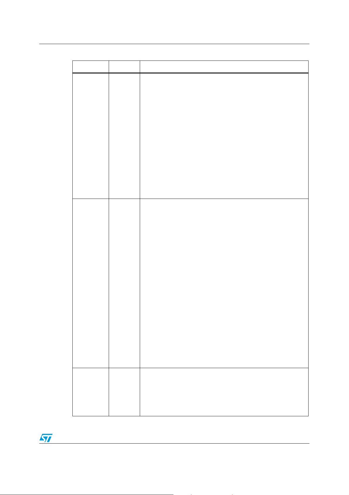
STM32F103x8, STM32F103xB Revision history
Table 60. Document revision history (continued)
Date Revision Changes
I/O information clarified on page 1.
Figure 3: STM32F103xx performance line LFBGA100 ballout modified.
Figure 10: Memory map modified. Table 4: Timer feature comparison
added.
PB4, PB13, PB14, PB15, PB3/TRACESWO moved from Default
column to Remap column in Table 5: Medium-density STM32F103xx
pin definitions.
for LFBGA100 corrected in Table 9: General operating conditions.
P
D
23-Apr-2009 10
22-Sep-2009 11
03-Jun-2010 12
Note modified in Table 13: Maximum current consumption in Run
mode, code with data processing running from Flash and Table 15:
Maximum current consumption in Sleep mode, code running from
Flash or RAM.
Table 20: High-speed external user clock characteristics and Ta bl e 2 1 :
Low-speed external user clock characteristics modified.
Figure 19 shows a typical curve (title modified). ACC
max values
HSI
modified in Table 24: HSI oscillator characteristics.
TFBGA64 package added (see Ta bl e 5 6 and Tab l e 5 0). Small text
changes.
Note 5 updated and Note 4 added in Table 5: Medium-density
STM32F103xx pin definitions.
V
RERINT
voltage. I
and T
DD_VBAT
added to Table 12: Embedded internal reference
Coeff
value added to Table 16: Typical and maximum
current consumptions in Stop and Standby modes. Figure 17: Typical
current consumption on VBAT with RTC on versus temperature at
different VBAT values added.
f
min modified in Table 20: High-speed external user clock
HSE_ext
characteristics.
and CL2 replaced by C in Table 22: HSE 4-16 MHz oscillator
C
L1
characteristics and Table 23: LSE oscillator characteristics (fLSE =
32.768 kHz), notes modified and moved below the tables. Tab le 2 4 : HS I
oscillator characteristics modified. Conditions removed from Ta b le 2 6 :
Low-power mode wakeup timings.
Note 1 modified below Figure 23: Typical application with an 8 MHz
crystal.
IEC 1000 standard updated to IEC 61000 and SAE J1752/3 updated to
IEC 61967-2 in Section 5.3.10: EMC characteristics on page 56.
Jitter added to Table 27: PLL characteristics.
Table 42: SPI characteristics modified.
and R
C
ADC
R
max values modified in Table 47: RAIN max for fADC = 14 MHz.
AIN
parameters modified in Table 46: ADC characteristics.
AIN
Figure 44: LFBGA100 - 10 x 10 mm low profile fine pitch ball grid array
package outline updated.
Added STM32F103TB devices.
Added VFQFPN48 package.
Updated note 2 below Table 40: I2C characteristics
Updated Figure 31: I2C bus AC waveforms and measurement circuit
Updated Figure 30: Recommended NRST pin protection
Updated Section 5.3.12: I/O current injection characteristics
Doc ID 13587 Rev 13 97/99

Revision history STM32F103x8, STM32F103xB
Table 60. Document revision history (continued)
Date Revision Changes
Updated footnotes below Table 6: Voltage characteristics on page 35
and Table 7: Current characteristics on page 36
Updated tw min in Table 20: High-speed external user clock
19-Apr-2011 13
characteristics on page 49
Updated startup time in Table 23: LSE oscillator characteristics (fLSE =
32.768 kHz) on page 52
Added Section 5.3.12: I/O current injection characteristics
Updated Section 5.3.13: I/O port characteristics
98/99 Doc ID 13587 Rev 13

STM32F103x8, STM32F103xB
Please Read Carefully:
Information in this document is provided solely in connection with ST products. STMicroelectronics NV and its subsidiaries (“ST”) reserve the
right to make changes, corrections, modifications or improvements, to this document, and the products and services described herein at any
time, without notice.
All ST products are sold pursuant to ST’s terms and conditions of sale.
Purchasers are solely responsible for the choice, selection and use of the ST products and services described herein, and ST assumes no
liability whatsoever relating to the choice, selection or use of the ST products and services described herein.
No license, express or implied, by estoppel or otherwise, to any intellectual property rights is granted under this document. If any part of this
document refers to any third party products or services it shall not be deemed a license grant by ST for the use of such third party products
or services, or any intellectual property contained therein or considered as a warranty covering the use in any manner whatsoever of such
third party products or services or any intellectual property contained therein.
UNLESS OTHERWISE SET FORTH IN ST’S TERMS AND CONDITIONS OF SALE ST DISCLAIMS ANY EXPRESS OR IMPLIED
WARRANTY WITH RESPECT TO THE USE AND/OR SALE OF ST PRODUCTS INCLUDING WITHOUT LIMITATION IMPLIED
WARRANTIES OF MERCHANTABILITY, FITNESS FOR A PARTICULAR PURPOSE (AND THEIR EQUIVALENTS UNDER THE LAWS
OF ANY JURISDICTION), OR INFRINGEMENT OF ANY PATENT, COPYRIGHT OR OTHER INTELLECTUAL PROPERTY RIGHT.
UNLESS EXPRESSLY APPROVED IN WRITING BY AN AUTHORIZED ST REPRESENTATIVE, ST PRODUCTS ARE NOT
RECOMMENDED, AUTHORIZED OR WARRANTED FOR USE IN MILITARY, AIR CRAFT, SPACE, LIFE SAVING, OR LIFE SUSTAINING
APPLICATIONS, NOR IN PRODUCTS OR SYSTEMS WHERE FAILURE OR MALFUNCTION MAY RESULT IN PERSONAL INJURY,
DEATH, OR SEVERE PROPERTY OR ENVIRONMENTAL DAMAGE. ST PRODUCTS WHICH ARE NOT SPECIFIED AS "AUTOMOTIVE
GRADE" MAY ONLY BE USED IN AUTOMOTIVE APPLICATIONS AT USER’S OWN RISK.
Resale of ST products with provisions different from the statements and/or technical features set forth in this document shall immediately void
any warranty granted by ST for the ST product or service described herein and shall not create or extend in any manner whatsoever, any
liability of ST.
ST and the ST logo are trademarks or registered trademarks of ST in various countries.
Information in this document supersedes and replaces all information previously supplied.
The ST logo is a registered trademark of STMicroelectronics. All other names are the property of their respective owners.
© 2011 STMicroelectronics - All rights reserved
STMicroelectronics group of companies
Australia - Belgium - Brazil - Canada - China - Czech Republic - Finland - France - Germany - Hong Kong - India - Israel - Italy - Japan -
Malaysia - Malta - Morocco - Philippines - Singapore - Spain - Sweden - Switzerland - United Kingdom - United States of America
www.st.com
Doc ID 13587 Rev 13 99/99
 Loading...