

www.DataSheet4U.com
查询STM32F101x6供应商查询STM32F101x6供应商
STM32F101x6
STM32F101x8 STM32F101xB
Access line, advanced ARM-based 32-bit MCU with Flash memory,
six 16-bit timers, ADC and seven communication interfaces
Preliminary Data
Features
■ Core: ARM 32-bit Cortex™-M3
– 36 MHz, 45 DMIPS with 1.25 DMIPS/MHz
– Single-cycle multiplication and hardware
division
– Nested interrupt controller with 43
maskable interrupt channels
– Interrupt processing (down to 6 CPU
cycles) with tail chaining
■ Memories
– 32-to -1 2 8 Kbytes of Flash me m ory
– 6-to- 16 Kbytes of SRAM
■ Clock, reset and supply management
– 2.0 to 3.6 V application supply and I/Os
– POR, PDR and programmable voltage
detector (PVD)
– 4-to-16 MHz high-speed quartz oscillator
– Internal 8 MHz factory-trimmed RC
– Internal 32 kHz RC
– PLL for CPU clock
– Dedicated 32 kHz oscillator for RTC with
calibration
■ Low power
– Sleep, Stop and Standby modes
–V
■ Debug mode
supply for RTC and backup registers
BAT
– Serial wire debug (SWD) and JTAG
interfaces
■ DMA
– 7-channel DMA controller
– Peripherals supported: timers, ADC, SPIs,
2
I
Cs and USARTs
■ 12-bit, 1 µs A/D converter (16-channel)
– Conversion range: 0 to 3.6 V
CPU
LQFP48
7 x 7 mm
LQFP64
10 x 10 mm
LQFP100
14 x 14 mm
– Temperature sensor
■ Up to 80 fast I/O ports
– 32/49/80 5 V-tolerant I/Os
– All mappable on 16 external interrupt
vectors
– Atomi c re ad /m o dif y/write operations
■ Up to 6 timers
– Up to three 16-bit timers, each with up to 4
IC/OC/PWM or pulse counter
– 2 x 16-bit watchdog timers (Independent
and Window)
– SysTick timer: 24-bit downcounter
■ Up to 7 communication interfaces
– Up to 2 x I
2
C interfaces (SMBus/PMBus)
– Up to 3 USARTs (ISO 7816 interface, LIN,
IrDA capability, modem control)
– Up to 2 SPIs (18 Mbit/s)
Table 1. Device summary
Reference Root part number
STM32F101x6 STM32F101C6, STM32F101R6
STM32F101x8
STM32F101xB STM32F101RB, STM32F101VB
STM32F101C8, STM32F101R8
STM32F101V8
July 2007 Rev 2 1/64
This is preliminary information on a new product now in development or undergoing ev aluation. Details are subject to
change without notice.
www.st.com
1

Contents STM32F101xx
Contents
1 Introduction . . . . . . . . . . . . . . . . . . . . . . . . . . . . . . . . . . . . . . . . . . . . . . . . 6
2 Description . . . . . . . . . . . . . . . . . . . . . . . . . . . . . . . . . . . . . . . . . . . . . . . . . 6
2.1 Device overview . . . . . . . . . . . . . . . . . . . . . . . . . . . . . . . . . . . . . . . . . . . . . 7
2.2 Overview . . . . . . . . . . . . . . . . . . . . . . . . . . . . . . . . . . . . . . . . . . . . . . . . . . 8
3 Pin descriptions . . . . . . . . . . . . . . . . . . . . . . . . . . . . . . . . . . . . . . . . . . . 14
4 Memory mapping . . . . . . . . . . . . . . . . . . . . . . . . . . . . . . . . . . . . . . . . . . 20
5 Electrical characteristics . . . . . . . . . . . . . . . . . . . . . . . . . . . . . . . . . . . . 21
5.1 Test conditions . . . . . . . . . . . . . . . . . . . . . . . . . . . . . . . . . . . . . . . . . . . . . 21
5.1.1 Minimum and maximum values . . . . . . . . . . . . . . . . . . . . . . . . . . . . . . . 21
5.1.2 Typical values . . . . . . . . . . . . . . . . . . . . . . . . . . . . . . . . . . . . . . . . . . . . . 21
5.1.3 Typical curves . . . . . . . . . . . . . . . . . . . . . . . . . . . . . . . . . . . . . . . . . . . . 21
5.1.4 Loading capacitor . . . . . . . . . . . . . . . . . . . . . . . . . . . . . . . . . . . . . . . . . 21
5.1.5 Pin input voltage . . . . . . . . . . . . . . . . . . . . . . . . . . . . . . . . . . . . . . . . . . 21
5.1.6 Power supply scheme . . . . . . . . . . . . . . . . . . . . . . . . . . . . . . . . . . . . . . 22
5.1.7 Current consumption measurement . . . . . . . . . . . . . . . . . . . . . . . . . . . 23
5.2 Absolute maximum ratings . . . . . . . . . . . . . . . . . . . . . . . . . . . . . . . . . . . . 24
5.3 Operating conditions . . . . . . . . . . . . . . . . . . . . . . . . . . . . . . . . . . . . . . . . 26
5.3.1 General operating conditions . . . . . . . . . . . . . . . . . . . . . . . . . . . . . . . . . 26
5.3.2 Operating conditions at power-up / power-down . . . . . . . . . . . . . . . . . . 26
5.3.3 Embedded reset and power control block characteristics . . . . . . . . . . . 27
5.3.4 Embedded reference voltage . . . . . . . . . . . . . . . . . . . . . . . . . . . . . . . . . 27
5.3.5 Supply current characteristics . . . . . . . . . . . . . . . . . . . . . . . . . . . . . . . . 28
5.3.6 External clock source characteristics . . . . . . . . . . . . . . . . . . . . . . . . . . . 32
5.3.7 Internal Clock source characteristics . . . . . . . . . . . . . . . . . . . . . . . . . . . 36
5.3.8 PLL characteristics . . . . . . . . . . . . . . . . . . . . . . . . . . . . . . . . . . . . . . . . 37
5.3.9 Memory characteristics . . . . . . . . . . . . . . . . . . . . . . . . . . . . . . . . . . . . . 38
5.3.10 EMC characteristics . . . . . . . . . . . . . . . . . . . . . . . . . . . . . . . . . . . . . . . . 39
5.3.11 Absolute maximum ratings (electrical sensitivity) . . . . . . . . . . . . . . . . . 40
5.3.12 I/O port characteristics . . . . . . . . . . . . . . . . . . . . . . . . . . . . . . . . . . . . . . 42
5.3.13 NRST pin characteristics . . . . . . . . . . . . . . . . . . . . . . . . . . . . . . . . . . . . 47
2/64

STM32F101xx Contents
5.3.14 TIM timer characteristics . . . . . . . . . . . . . . . . . . . . . . . . . . . . . . . . . . . . 48
5.3.15 Communications interfaces . . . . . . . . . . . . . . . . . . . . . . . . . . . . . . . . . . 49
5.3.16 12-bit ADC characteristics . . . . . . . . . . . . . . . . . . . . . . . . . . . . . . . . . . . 54
5.3.17 Temperature sensor characteristics . . . . . . . . . . . . . . . . . . . . . . . . . . . . 57
6 Package characteristics . . . . . . . . . . . . . . . . . . . . . . . . . . . . . . . . . . . . . 58
6.1 Thermal characteristics . . . . . . . . . . . . . . . . . . . . . . . . . . . . . . . . . . . . . . 61
7 Order codes . . . . . . . . . . . . . . . . . . . . . . . . . . . . . . . . . . . . . . . . . . . . . . . 62
7.1 Future family enhancements . . . . . . . . . . . . . . . . . . . . . . . . . . . . . . . . . . 62
8 Revision history . . . . . . . . . . . . . . . . . . . . . . . . . . . . . . . . . . . . . . . . . . . 63
3/64

List of tables STM32F101xx
List of tables
Table 1. Device summary. . . . . . . . . . . . . . . . . . . . . . . . . . . . . . . . . . . . . . . . . . . . . . . . . . . . . . . . . . 1
Table 2. Device features and peripheral counts (STM32F101xx access line) . . . . . . . . . . . . . . . . . . 7
Table 3. Pin definitions . . . . . . . . . . . . . . . . . . . . . . . . . . . . . . . . . . . . . . . . . . . . . . . . . . . . . . . . . . . 16
Table 4. Voltage characteristics . . . . . . . . . . . . . . . . . . . . . . . . . . . . . . . . . . . . . . . . . . . . . . . . . . . . 24
Table 5. Current characteristics . . . . . . . . . . . . . . . . . . . . . . . . . . . . . . . . . . . . . . . . . . . . . . . . . . . . 24
Table 6. Thermal characteristics. . . . . . . . . . . . . . . . . . . . . . . . . . . . . . . . . . . . . . . . . . . . . . . . . . . . 25
Table 7. General operating conditions . . . . . . . . . . . . . . . . . . . . . . . . . . . . . . . . . . . . . . . . . . . . . . . 26
Table 8. Operating conditions at power-up / power-down . . . . . . . . . . . . . . . . . . . . . . . . . . . . . . . . 26
Table 9. Embedded reset and power control block characteristics. . . . . . . . . . . . . . . . . . . . . . . . . . 27
Table 10. Embedded internal reference voltage. . . . . . . . . . . . . . . . . . . . . . . . . . . . . . . . . . . . . . . . . 27
Table 11. Maximum current consumption in Run and Sleep modes (T
Table 12. Maximum current consumption in Stop and Standby modes . . . . . . . . . . . . . . . . . . . . . . . 29
Table 13. Typical current consumption in Run and Sleep modes . . . . . . . . . . . . . . . . . . . . . . . . . . . 30
Table 14. Typical current consumption in Stop and Standby modes . . . . . . . . . . . . . . . . . . . . . . . . . 31
Table 15. High-speed user external (HSE) clock characteristics . . . . . . . . . . . . . . . . . . . . . . . . . . . . 32
Table 16. Low-speed user external clock characteristics . . . . . . . . . . . . . . . . . . . . . . . . . . . . . . . . . . 32
Table 17. HSE 4-16 MHz oscillator characteristics. . . . . . . . . . . . . . . . . . . . . . . . . . . . . . . . . . . . . . . 34
Table 18. LSE oscillator characteristics (
= 32.768 kHz) . . . . . . . . . . . . . . . . . . . . . . . . . . . . . . . 35
fLSE
Table 19. HSI oscillator characteristics. . . . . . . . . . . . . . . . . . . . . . . . . . . . . . . . . . . . . . . . . . . . . . . . 36
Table 20. LSI oscillator characteristics . . . . . . . . . . . . . . . . . . . . . . . . . . . . . . . . . . . . . . . . . . . . . . . 36
Table 21. Low-power mode wakeup timings . . . . . . . . . . . . . . . . . . . . . . . . . . . . . . . . . . . . . . . . . . . 37
Table 22. PLL characteristics . . . . . . . . . . . . . . . . . . . . . . . . . . . . . . . . . . . . . . . . . . . . . . . . . . . . . . . 37
Table 23. Flash memory characteristics. . . . . . . . . . . . . . . . . . . . . . . . . . . . . . . . . . . . . . . . . . . . . . . 38
Table 24. Flash endurance and data retention. . . . . . . . . . . . . . . . . . . . . . . . . . . . . . . . . . . . . . . . . . 38
Table 25. EMS characteristics . . . . . . . . . . . . . . . . . . . . . . . . . . . . . . . . . . . . . . . . . . . . . . . . . . . . . . 39
Table 26. EMI characteristics . . . . . . . . . . . . . . . . . . . . . . . . . . . . . . . . . . . . . . . . . . . . . . . . . . . . . . . 40
Table 27. ESD absolute maximum ratings . . . . . . . . . . . . . . . . . . . . . . . . . . . . . . . . . . . . . . . . . . . . . 40
Table 28. Electrical sensitivities . . . . . . . . . . . . . . . . . . . . . . . . . . . . . . . . . . . . . . . . . . . . . . . . . . . . . 41
Table 29. I/O static characteristics . . . . . . . . . . . . . . . . . . . . . . . . . . . . . . . . . . . . . . . . . . . . . . . . . . . 42
Table 30. Output voltage characteristics . . . . . . . . . . . . . . . . . . . . . . . . . . . . . . . . . . . . . . . . . . . . . . 44
Table 31. I/O AC characteristics. . . . . . . . . . . . . . . . . . . . . . . . . . . . . . . . . . . . . . . . . . . . . . . . . . . . . 45
Table 32. NRST pin characteristics . . . . . . . . . . . . . . . . . . . . . . . . . . . . . . . . . . . . . . . . . . . . . . . . . . 47
Table 33. TIMx characteristics . . . . . . . . . . . . . . . . . . . . . . . . . . . . . . . . . . . . . . . . . . . . . . . . . . . . . . 48
Table 34. I
Table 35. SCL frequency (f
2
C characteristics. . . . . . . . . . . . . . . . . . . . . . . . . . . . . . . . . . . . . . . . . . . . . . . . . . . . . . . . 49
= 36 MHz, VDD = 3.3 V) . . . . . . . . . . . . . . . . . . . . . . . . . . . . . . . . . 50
PCLK1
Table 36. SPI characteristics . . . . . . . . . . . . . . . . . . . . . . . . . . . . . . . . . . . . . . . . . . . . . . . . . . . . . . . 51
Table 37. ADC characteristics . . . . . . . . . . . . . . . . . . . . . . . . . . . . . . . . . . . . . . . . . . . . . . . . . . . . . . 54
Table 38. ADC accuracy (f
PCLK2
= 10 MHz, f
= 10 MHz, R
ADC
AIN
Table 39. TS characteristics . . . . . . . . . . . . . . . . . . . . . . . . . . . . . . . . . . . . . . . . . . . . . . . . . . . . . . . . 57
Table 40. LQPF100 – 100-pin low-profile quad flat package mechanical data . . . . . . . . . . . . . . . . . 58
Table 41. LQFP64 – 64-pin low-profile quad flat package mechanical data . . . . . . . . . . . . . . . . . . . 59
Table 42. LQFP48 – 48-pin low-profile quad flat package mechanical data . . . . . . . . . . . . . . . . . . . 60
Table 43. Thermal characteristics. . . . . . . . . . . . . . . . . . . . . . . . . . . . . . . . . . . . . . . . . . . . . . . . . . . . 61
Table 44. Order codes . . . . . . . . . . . . . . . . . . . . . . . . . . . . . . . . . . . . . . . . . . . . . . . . . . . . . . . . . . . . 62
Table 45. Document revision history . . . . . . . . . . . . . . . . . . . . . . . . . . . . . . . . . . . . . . . . . . . . . . . . . 63
= 85 °C) . . . . . . . . . . . . . . . 28
A
< 10 kΩ, V
= 3.3 V) . . . . . . . . 55
DDA
4/64

STM32F101xx List of figures
List of figures
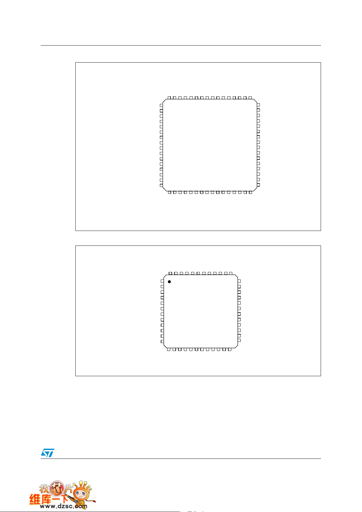
Figure 1. STM32F101xx access line block diagram . . . . . . . . . . . . . . . . . . . . . . . . . . . . . . . . . . . 13
Figure 2. STM32F101xx access line LQFP100 pinout . . . . . . . . . . . . . . . . . . . . . . . . . . . . . . . . . . . 14
Figure 3. STM32F101xx access line LQFP64 pinout . . . . . . . . . . . . . . . . . . . . . . . . . . . . . . . . . . . . 15
Figure 4. STM32F101xx access line LQFP48 pinout . . . . . . . . . . . . . . . . . . . . . . . . . . . . . . . . . . . . 15
Figure 5. Memory map. . . . . . . . . . . . . . . . . . . . . . . . . . . . . . . . . . . . . . . . . . . . . . . . . . . . . . . . . . . . 20
Figure 6. Pin loading conditions. . . . . . . . . . . . . . . . . . . . . . . . . . . . . . . . . . . . . . . . . . . . . . . . . . . . . 22
Figure 7. Pin input voltage . . . . . . . . . . . . . . . . . . . . . . . . . . . . . . . . . . . . . . . . . . . . . . . . . . . . . . . . . 22
Figure 8. Power supply scheme. . . . . . . . . . . . . . . . . . . . . . . . . . . . . . . . . . . . . . . . . . . . . . . . . . . . . 22
Figure 9. Current consumption measurement scheme . . . . . . . . . . . . . . . . . . . . . . . . . . . . . . . . . . . 23
Figure 10. High-speed external clock source AC timing diagram . . . . . . . . . . . . . . . . . . . . . . . . . . . . 33
Figure 11. Low-speed external clock source AC timing diagram. . . . . . . . . . . . . . . . . . . . . . . . . . . . . 33
Figure 12. Typical application with an 8 MHz crystal. . . . . . . . . . . . . . . . . . . . . . . . . . . . . . . . . . . . . . 34
Figure 13. Typical application with a 32.768 kHz crystal . . . . . . . . . . . . . . . . . . . . . . . . . . . . . . . . . . . 35
Figure 14. Unused I/O pin connection . . . . . . . . . . . . . . . . . . . . . . . . . . . . . . . . . . . . . . . . . . . . . . . . . 43
Figure 15. I/O AC characteristics definition . . . . . . . . . . . . . . . . . . . . . . . . . . . . . . . . . . . . . . . . . . . . . 46
Figure 16. Recommended NRST pin protection . . . . . . . . . . . . . . . . . . . . . . . . . . . . . . . . . . . . . . . . . 47
Figure 17. I
Figure 18. SPI timing diagram - slave mode and CPHA=0 . . . . . . . . . . . . . . . . . . . . . . . . . . . . . . . . . 52
Figure 19. SPI timing diagram - slave mode and CPHA=11). . . . . . . . . . . . . . . . . . . . . . . . . . . . . . . . 52
Figure 20. SPI timing diagram - master mode . . . . . . . . . . . . . . . . . . . . . . . . . . . . . . . . . . . . . . . . . . . 53
Figure 21. ADC accuracy characteristics. . . . . . . . . . . . . . . . . . . . . . . . . . . . . . . . . . . . . . . . . . . . . . . 55
Figure 22. Typical connection diagram using the ADC . . . . . . . . . . . . . . . . . . . . . . . . . . . . . . . . . . . . 55
Figure 23. Power supply and reference decoupling (V
Figure 24. Power supply and reference decoupling (VREF+ connected to VDDA). . . . . . . . . . . . . . . 56
Figure 25. LQPF100 – 100-pin low-profile quad flat package outline . . . . . . . . . . . . . . . . . . . . . . . . . 58
Figure 26. LQFP64 – 64-pin low-profile quad flat package outline . . . . . . . . . . . . . . . . . . . . . . . . . . . 59
Figure 27. LQFP48 – 48-pin low-profile quad flat package outline . . . . . . . . . . . . . . . . . . . . . . . . . . . 60
2
C bus AC waveforms and measurement circuit . . . . . . . . . . . . . . . . . . . . . . . . . . . . . . . 50
not connected to V
REF+
). . . . . . . . . . . . . . 56
DDA
5/64
Introduction STM32F101xx
1 Introduction
This datasheet contains the description of the STM32F101xx access line family features,
pinout, Electrical Characteristics, Mechanical Data and Ordering information.
For information on programming, erasing and protection of the internal Flash memory
please refer to the STM32F10x Flash Programming Reference Manual
For information on the Cortex™-M3 core please refer to the Cortex™-M3 Technical
Reference Manual.
2 Description
The STM32F101xx access line family incorporates the high- performance ARM Cortex™-M3
32-bit RISC core operating at a 36 MHz frequency, high-speed embedded memories (Flash
memory up to 128Kbytes and SRAM up to 16 Kbytes), and an extensive ran ge of enhanced
peripherals and I/Os connected to tw o APB bu ses. All de vices off er standard comm unication
interfaces (two I
purpose 16-bit timers.
2
Cs, two SPIs, a nd up to three USARTs), one 12-bit ADC and three g ener al
The STM32F101 family oper at es in the −40 to +85°C temperature range , from a 2.0 to 3. 6 V
power supply. A comprehensive set of power-saving mode allows to design low-power
applications.
The complete STM32F101xx access line family includes devices in 3 different package
types: from 48 pins to 100 pins. Depending on the device chosen, different sets of
peripherals are included, the description below gives an overview of the complete range of
peripherals proposed in this family.
These features make the STM32F101xx access line microcontroller family suitable for a
wide range of applications:
● Application control and user interface
● Medical and handheld equipment
● PC peripherals, gaming and GPS platforms
● Industrial applications: PLC, inverters, printers, and scanners
● Alarm systems, Video intercom, and HVAC
Figure 1 shows the general block diagram of the device family.
6/64

STM32F101xx Description
2.1 Device overview
Table 2. Device features and peripheral counts (STM32F101xx access line)
Peripheral
Flash - Kbytes 32 64 32 64 128 64 128
SRAM - Kbytes 610610161016
General purpose 23 3 3
Timers
SPI 121 2 2
2
C 121 2 2
I
USART 232 3 3
Communication
12-bit synchronized ADC
number of channels
GPIOs 32 49 80
STM32F101Cx STM32F101Rx STM32F101Vx
1
10 channels
1
16 channels
CPU frequency 36 MHz
Operating voltage 2.0 to 3.6 V
Operating temperature -40 to +85 °C
Packages LQFP48 LQFP64 LQFP100
7/64

Description STM32F101xx
2.2 Overview
ARM® CortexTM-M3 core with embedded Flash and SRAM
The ARM Cortex™-M3 processor is the latest generation of ARM processors for embedded
systems. It has been de v eloped t o prov ide a low- cost platform that meets the needs of MCU
implementation, with a reduced pin count and low-power consumption, while delivering
outstanding computational performance and an advanced system response to interrupts.
The ARM Cortex™-M3 32-bit RISC processor features exceptional code-efficiency,
delivering the high-performance expected from an ARM core in the memory size usually
associated with 8- and 16-bit devices.
The STM32F101xx access line family having an embedded ARM core, is therefore
compatible with all ARM tools and software.
Embedded Flash memory
Up to 128 Kbytes of embedded Flash is available for storing programs and data.
Embedded SRAM
Up to 16 Kbytes of embedded SRAM accessed (read/write) at CPU clock speed with 0 wait
states.
Nested vectored interrupt controller (NVIC)
The STM32F101xx access line embeds a nested vectored interrupt controller able to handle
up to 43 maskable interrupt channels (not including the 16 interrupt lines of Cortex™-M3)
and 16 priority levels.
● Closely coupled NVIC gives low latency interrupt processing
● Interrupt entry vector table address passed directly to the core
● Closely coupled NVIC core interface
● Allows early processing of interrupts
● Processing of late arriving higher priority inte r rupts
● Support for tail-chaining
● Processor state automatically saved
● Interrupt entry restored on interrupt exit with no instruction overhead
This hardware block provides flexible interrupt management features with minimal interrupt
latency.
8/64

STM32F101xx Description
External interrupt/event controller (EXTI)
The external interrupt/event controller consists of 19 edge detectors lines used to generate
interrupt/event requests. Each line can be independently configured to select the trigger
event (rising edge , falling edge, both) and ca n be mask ed ind ependently. A pending register
maintains the status of the interrupt requests. The EXTI can detect external line with pulse
width lower than the Internal APB2 clock period. Up to 80 GPIOs are connected to the 16
external interrupt lines.
Clocks and startup
System clock selection is performed on startup, however the internal RC 8 MHz oscillator is
selected as default CPU clock on reset. An external 4-16 MHz clock can be selected and is
monitored for failure. During such a scenario, it is disabled and software interrupt
management follo ws . Similarly, full interrupt management of the PLL clock entry is av ailable
when necessary (for example with failure of an indirectly used external oscillator).
Several prescalers allow the configuration of the AHB frequency, the High Speed APB
(APB2) and the low Speed APB (APB1) domains. The maximum frequency of the AHB and
the APB domains is 36 MHz.
Boot modes
At startup, boot pins are used to select one of five boot options:
● Boot from User Flash
● Boot from System Memory
● Boot from SRAM
The boot loader is located in System Memory. It is used to reprogram the Flash memory by
using the USART.
Power supply schemes
● V
● V
● V
= 2.0 to 3.6 V: External power sup ply for I/Os and the internal regulator.
DD
Provided externally through V
, V
SSA
and PLL. In V
BAT
= 2.0 to 3.6 V: External analog power sup plies for ADC, Reset b loc ks , RCs
DDA
range (ADC is limited at 2.4 V).
DD
= 1.8 to 3.6 V: Power supply for RTC, external clock 32 kHz oscillator and backup
registers (through power switch) when V
DD
pins.
is not present.
DD
Power supply supervisor
The device has an integrated power on reset (POR)/power down reset (PDR) circuitry. It is
always active, and ensures proper operation starting from/down to 2 V. The device remains
in reset mode when V
external reset circuit.
The device features an embedded Programmable voltage detector (PVD) that monitors the
V
power supply and compares it to the V
DD
when V
drops below the V
DD
interrupt service routine can then generate a warning message and/or put the MCU into a
safe state. The PVD is enabled by software.
Refer to Table 9: Embedded reset and power control block characteristics for the values of
V
POR/PDR
and V
PVD
is below a specified threshold, V
DD
and/or when VDD is higher than the V
PVD
PVD
.
POR/PDR
, without the need for an
threshold. An interrupt can be generated
threshold. The
PVD
9/64

Description STM32F101xx
Voltage regulator
The regulator has three operation modes: ma in (M R ), low power (LPR) and power down.
● MR is used in the nominal regulation mode (Run)
● LPR is used in the Stop modes
● Power down is used in Standby Mode: the regulator output is in high impedance: the
kernel circuitry is powered-down, inducing zero consumption (but the contents of the
registers and SRAM are lost)
This regulator is always enabled after RESET. It is disabled in Standby Mode, providing high
impedance output.
Low-power modes
The STM32F101xx access line supports three low-power modes to achieve the best
compromise between low power consumption, short startup time and available wakeup
sources:
● Sleep mode
In Sleep mode, only the CPU is stopped. All peripherals continue to operate and can
wake up the CPU when an interrupt/event occurs.
● Stop mode
Stop mode allows to achieve the lowest po we r consumption while re taining the co ntent
of SRAM and registers. All clocks in the 1.8 V domain are stopped, the PLL, the HSI
and the HSE RC oscillators are disabled. The voltage regulator can also be put either in
normal or in low power mode.
The device can be wok en up from Stop mode by any of the EXTI line. The EXTI line
source can be one of the 16 external lines, the PVD output or the RTC alarm.
● Standby mode
The Standby mode allows to achieve the lo west power consumption. The internal
voltage regulator is switched off so that the entire 1.8 V domain is powered off. The
PLL, the HSI and the HSE RC oscillators are also switched off. After entering Standby
mode, SRAM and registers content are lost except for registers in the Backup domain
and Standby circuitry.
The device exits Standby mode when an external reset (NRST pin), a IWDG reset, a
rising edge on the WKUP pin, or an RTC alarm occurs.
Note: The RTC , the IWDG, and t he corresponding cloc k sources ar e not stopped by e ntering Stop
or Standby mode.
DMA
The flexible 7-channel general-purpose DMA is able to manage memory-to-memory,
peripheral-to-memory and memory-to-peripheral transfers. The DMA controller supports
circular buffer management avoiding the generation of interrupts when the controller
reaches the end of the buffer.
Each channel is connected to dedicated hardware DMA requests, with support for software
trigger on each channel. Configuration is made by software and transfer sizes between
source and destination are independent.
The DMA can be used with the main peripherals: SPI, I
TIMx and ADC.
10/64
2
C, USART, general purpose timers

STM32F101xx Description
RTC (real-time clock) and backup registers
The RTC and the bac kup registers are supplied through a switch that takes po wer either on
V
supply when present or through the V
DD
can be used to store data when V
power is not present.
DD
pin. The backup registers (ten 16-bit registers)
BAT
The Real-Time Clock provides a set of continuously running counters which can be used
with suitable software to provide a clock calendar function, and provides an alarm interrupt
and a periodic interrupt. It is clocked by an external 32.768 kHz oscillator, the internal low
power RC oscillator or the high-speed external clock divided by 128. The internal low pow er
RC has a typical frequency of 32 kHz. The RTC can be calibrated using an external 512Hz
output to compensate for any natural quartz deviation. The RTC features a 32-bit
programmable counter for long term measurement using the Compare register to generate
an alarm. A 20-bit prescaler is used for the time base clock and is by default configured to
generate a time base of 1 second from a clock at 32.768 kHz.
Independent watchdog
The independent watchdog is based on a 12-bit downcounter and 8-bit prescaler. It is
clocked from an independent 32 kHz internal RC and as it operates independently from the
main clock, it can operate in Stop and Standby modes. It can be used as a watchdog to
reset the device when a problem occurs, or as a free running timer for application time out
management. It is hardware o r software configurable through the option bytes. The counter
can be frozen in debug mode.
Window watchdog
The window watchdog is based on a 7-bit downcounter that can be set as free running. It
can be used as a watchdog to reset the de vice when a prob lem occurs . It is clock ed from the
main clock. It has an early warning interrupt capability and the counter can be frozen in
debug mode.
SysTick timer
This timer is dedicated for OS, but could also be used as a standard down counter. It
features:
● A 24-bit down counter
● Autoreload capability
● Maskable system interrupt generation whe n th e co un te r re ach e s 0.
● Programmable clock source
General purpose timers (TIMx)
There are up to 3 synchronizable standard timers embedded in the STM32F101xx access
line devices. These timers are based on a 16-bit auto-reload up/down counter, a 16-bit
prescaler and feature 4 in dependent channels each f or input captu re, output compa re, PWM
or one pulse mode output. This give s u p to 12 input ca ptur es / o utpu t compar es / PWMs on
the largest packages. They can work together via the Timer Link feature for synchronization
or event chaining.
The counter can be frozen in debug mode.
Any of the standard timers can be used to generate PWM outputs. Each of the timers has
independent DMA request generations.
11/64

Description STM32F101xx
I²C bus
Up to two I²C bus interf aces can oper ate in multi-maste r and slav e modes . They can sup port
standard and fast modes.
They support dual slave addressing (7-bit only) and both 7/10-bit addressing in master
mode. A hardware CRC generation/verification is embedded.
They can be served by DMA and they support SM Bus 2.0/PM Bus.
Universal synchronous/asynchronous receiver transmitter (USART)
The available USART interfaces communicate at up to 2.25 Mbit/s. They provide hardware
management of the CTS and RTS signals, support IrDA SIR ENDEC, are ISO 7816
compliant and have LIN Master/Slave capability.
The USART interfaces can be served by the DMA controller.
Serial peripheral interface (SPI)
Up to two SPIs are able to communicate up to 18 Mbits/s in slave and master modes in fullduplex and simplex communication modes. The 3-bit prescaler gives 8 master mode
frequencies and the frame is configurable from 8-bit to 16-bit. The hardware CRC
generation/ve rification supports basic SD Card/MMC modes.
Both SPIs can be served by the DMA controller.
GPIOs (general purpose inputs/outputs)
Each of the GPIO pins can be configured b y softw are as output ( push-pull or open-dr ain), as
input (with or without pull-up or pull-down) or as Peripheral Alternate Function. Most of the
GPIO pins are shared with digital or analog alternate functions. All GPIOs are high currentcapable.
The I/Os alternate function configuration can be locked if needed following a specific
sequence in order to avoid spurious writing to the I/Os registers.
ADC (analog to digital converter)
The 12-bit Analog to Digital Converter has up to 16 external channels and performs
conversions in single-shot or scan modes. In scan mode, automatic conversion is performed
on a selected group of analog inputs.
The ADC can be served by the DMA controller.
An analog watchdog f eatur e allo ws very precise monitoring of the converted voltage of one ,
some or all selected channels. An interrupt is generated when the converted voltage is
outside the programmed thresholds.
Temperature sensor
The temperature sensor has to generate a linear voltage with any variation in temperature.
The conversion range is between 2V < V
connected to the ADC_IN16 input channel which is used to convert the sensor output
voltage into a digital value.
< 3.6V. The temperature sensor is internally
DDA
12/64
STM32F101xx Description
Serial wire JTAG debug port (SWJ-DP)
The ARM SWJ-DP Interface is embedded. and is a combined JTAG and serial wire debug
port that enables either a serial wire debug or a JTAG probe to be connected to the target.
The JTAG TMS and TCK pins are shared respectively with SWDIO and SWCLK and a
specific sequence on the TMS pin is used to switch between JTAG-DP and SW-DP.
Figure 1. STM32F101xx access line block diagram
JNTRST
JTDI
JTCK/SWCLK
JTMS/SWDIO
JTDO
as AF
80AF
PA[15:0]
PB[15:0]
PC[15:0]
PD[15:0]
PE[15:0]
MOSI,MISO,
SCK,NSS as AF
RX,TX, CTS, RTS,
SmartCard as AF
16AF
V
REF+
V
REF-
NRST
VDDA
VSSA
JTAG & SWD
Cortex M3 CPU
F
max
NVIC
NVIC
7 channels
SUPERVISION
POR / PDR
EXTI
WAKEUP
GPIOA
GPIOB
GPIOC
GPIOD
GPIOE
SPI1
USART1
@VDDA
12bit ADC1
Temp sensor
: 36 MHz
GP DMA
@VDDA
SUPPLY
PVD
IF
pbus
Dbus
System
Rst
Int
Ibus
= 36 MHz
max
APB2 : F
BusMatrix
Controller
AHB2
APB2
Trace
=36 MHz
max
AHB:F
obl
FLASH 128 KB
Interface
Flash
SRAM
16 KB
PCLK1
PCLK2
HCLK
FCLK
RC 8 MHz
RC 32 kHz
@VDDA
AHB2
APB1
64 bit
CLOCK
MANAGT
PLL &
=24 / 36 MHz
max
APB1 : F
@VBAT
Backup interface
2x(8x16bit)
POWER
VOLT. REG.
3.3V TO 1.8V
@VDD
@VDD
XTAL OSC
4-16 MHz
IWDG
Standby
interface
XTAL 32 kHz
Backup
RTC
AWU
TIM2
TIM3
TIM4
USART2
USART3
SPI2
I2C1
I2C2
W W D G
reg
V
= 2 to 3.6V
DD
V
SS
OSC_IN
OSC_OUT
V
BAT
OSC32_IN
OSC32_OUT
ANTI_TAMP
4 Channels
4 Channels
4 Channels
RX,TX, CTS, RTS,
SmartCard as AF
RX,TX, CTS, RTS,
SmartCard as AF
MOSI,MISO,SCK,NSS
as AF
SCL,SDA,SMBAL
as AF
SCL,SDA
as AF
1. AF = alternate function on I/O port pin.
2. TA = –40 °C to +85 °C (junction temperature up to 125 °C).
13/64
ai14385
Pin descriptions STM32F101xx
3 Pin descriptions
Figure 2. STM32F101xx access line LQFP100 pinout
VDD_3
VSS_3
PE1
PE0
PB9
PB8
BOOT0
PB7
PB6
PB5
PB4
PB3
PD7
PD6
PD5
PD4
PD3
PD2
PD1
PD0
PC12
PC11
PC10
PA15
PA14
PE2
PE3
PE4
PE5
PE6
VBAT
PC13-ANTI_TAMP
PC14-OSC32_IN
PC15-OSC32_OUT
VSS_5
VDD_5
OSC_IN
OSC_OUT
NRST
PC0
PC1
PC2
PC3
VSSA
VREF-
VREF+
VDDA
PA0-WKUP
PA1
PA2
100999897969594939291908988878685848382818079787776
1
2
3
4
5
6
7
8
9
10
11
12
13
14
15
16
17
18
19
20
21
22
23
24
25
26272829303132333435363738394041424344454647484950
PA3
PA4
PA5
PA6
PA7
VSS_4
VDD_4
PC4
PC5
PB0
LQFP100
PB1
PB2
PE7
PE8
PE9
PE10
PE11
PE12
PE13
PE14
PE15
PB10
PB11
VSS_1
75
VDD_2
74
VSS_2
73
NC
72
PA 13
71
PA 12
70
PA 11
69
PA 10
68
PA 9
67
PA 8
66
PC9
65
PC8
64
PC7
63
PC6
62
PD15
61
PD14
60
PD13
59
PD12
58
PD11
57
PD10
56
PD9
55
PD8
54
PB15
53
PB14
52
PB13
51
PB12
VDD_1
14/64
ai14386
STM32F101xx Pin descriptions
Figure 3. STM32F101xx access line LQFP64 pinout
VDD_3
VSS_3
PB9
PB8
BOOT0
PB7
PB6
PB5
PB4
PB3
PD2
PC12
PC11
PC10
PA15
PA14
PC13-ANTI_T AMP
VBAT
PC14-OSC32_IN
PC15-OSC32_OUT
PD0 OSC_IN
PD1 OSC_OUT
NRST
PC0
PC1
PC2
PC3
VSSA
VDDA
PA0-WKUP
PA1
PA2
64 63 62 61 60 59 58 57 56 55 54 53 52 51 50 49
1
2
3
4
5
6
7
8
9
10
11
12
13
14
15
16
17 18 19 20 21 22 23 24 29 30 31 3225 26 27 28
PA3
VSS_4
VDD_4
PA4
PA5
PA6
LQFP64
PA7
PC4
PC5
PB0
PB1
PB2
PB10
PB11
VDD_2
48
VSS_2
47
PA13
46
PA12
45
PA11
44
PA10
43
PA9
42
PA8
41
PC9
40
PC8
39
PC7
38
PC6
37
PB15
36
PB14
35
PB13
34
33
PB12
VSS_1
VDD_1
Figure 4. STM32F101xx access line LQFP48 pinout
VDD_3
VSS_3
PB9
PB8
BOOT0
PB7
PB6
PB5
PB4
PB3
PC13-ANTI_TAMP
VBAT
PC14-OSC32_IN
PC15-OSC32_OUT
PD0 OSC_IN
PD1 OSC_OUT
NRST
VSSA
VDDA
PA0-WKUP
PA1
PA2
48 47 46 45
1
2
3
4
5
6
7
8
9
10
11
12
13 14 15 16 17 18
PA3
44 43 42 41 40 39 38 37
LQFP48
19 20 21 22
PA4
PA5
PA6
PA7
PB0
PB1
PB2
PB10
23
PB11
VSS_1
ai14387
PA15
PA14
VDD_2
36
VSS_2
35
PA13
34
PA12
33
PA11
32
PA10
31
PA9
30
PA8
29
PB15
28
PB14
27
26
PB13
25
PB12
24
VDD_1
ai14378
15/64
Pin descriptions STM32F101xx
LQFP64
(2)
(1)
Pin name
Type
LQFP100
SV
BAT
(4)
(4)
(4)
SS_5
DD_5
I/O PC13 ANTI_TAMP
I/O
I/O
SV
SV
I / O level
FT
FT
FT
FT
FT
Main
function
(after reset)
PE2 TRACECK
PE3 TRACED0
PE4 TRACED1
PE5 TRACED2
PE6 TRACED3
PC14-
OSC32_IN
PC15-
OSC32_OUT
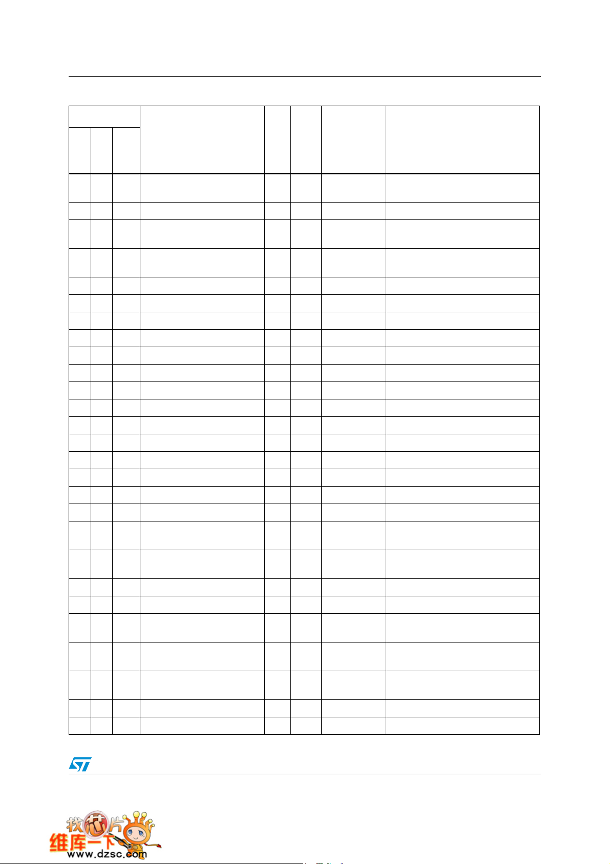
Table 3. Pin definitions
Pins
LQFP48
- - 1 PE2/TRACECK I/O
- - 2 PE3/TRACED0 I/O
- - 3 PE4/TRACED1 I/O
- - 4 PE5/TRACED2 I/O
- - 5 PE6/TRACED3 I/O
11 6 V
2 2 7 PC13-ANTI_TAMP
3 3 8 PC14-OSC32_IN
4 4 9 PC15-OSC32_OUT
--10 V
--11 V
5 5 12 OSC_IN I OSC_IN
BAT
SS_5
DD_5
(3)
Default alternate functions
(3)
6 6 13 OSC_OUT O OSC_OUT
7 7 14 NRST I/O NRST
- 8 15 PC0/ADC_IN10 I/O PC0 ADC_IN10
- 9 16 PC1/ADC_IN11 I/O PC1 ADC_IN11
- 10 17 PC2/ADC_IN12 I/O PC2 ADC_IN12
- 11 18 PC3/ADC_IN13 I/O PC3 ADC_IN13
81219 V
SSA
SV
SSA
- - 20 VREF- S VREF-
- - 21 VREF+ S VREF+
91322 V
10 14 23
11 15 24
12 16 25
13 17 26
PA0-WKUP/USART2_CTS/
ADC_IN0/TIM2_CH1_ETR
PA1/USART2_RTS/ADC_
PA2/USART2_TX/ADC_IN2/
PA3/USART2_RX/ADC_IN3/
-1827 V
-1928 V
DDA
IN1/TIM2_CH2
TIM2_CH3
TIM2_CH4
SS_4
DD_4
SV
I/O PA0
DDA
WKUP/USART2_CTS
I/O PA1
I/O PA2
I/O PA3
SV
SV
SS_4
DD_4
TIM2_CH1_ETR
USART2_RTS
TIM2_CH2
USART2_TX
TIM2_CH3
USART2_RX
TIM2_CH4
(7)
/ ADC_IN0/
(7)
/ADC_IN1/
(7)
(7)
/ADC_IN2/
(7)
(7)
/ADC_IN3/
(7)
(7)
16/64
STM32F101xx Pin descriptions
Table 3. Pin definitions (continued)
Pins
LQFP48
LQFP64
14 20 29
Pin name
LQFP100
PA4/SPI1_NSS/
USART2_CK/ADC_IN4
I/O PA4
(1)
(2)
Type
Main
function
(3)
(after reset)
Default alternate functions
I / O level
SPI1_NSS/USART2_CK
ADC_IN4
15 21 30 PA5/SPI1_SCK/ADC_IN5 I/O PA5 SPI1_SCK/ADC_IN5
16 22 31
17 23 32
PA6/SPI1_MISO/ADC_IN6/
TIM3_CH1
PA7/SPI1_MOSI/ADC_IN7/
TIM3_CH2
I/O PA6
I/O PA7
SPI1_MISO/ADC_IN6/
TIM3_CH1
SPI1_MOSI/ADC_IN7/
TIM3_CH2
(7)
(7)
- 24 33 PC4/ADC_IN14 I/O PC4 ADC_IN14
- 25 34 PC5/ADC_IN15 I/O PC5 ADC_IN15
18 26 35 PB0/ADC_IN8/TIM3_CH3 I/O PB0 ADC_IN8/TIM3_CH3
19 27 36 PB1/ADC_IN9/TIM3_CH4 I/O PB1 ADC_IN9/TIM3_CH4
(7)
(7)
20 28 37 PB2/BOOT1 I/O FT PB2/BOOT1
- - 38 PE7 I/O FT PE7
- - 39 PE8 I/O FT PE8
- - 40 PE9 I/O FT PE9
(7)
(3)
/
- - 41 PE10 I/O FT PE10
- - 42 PE11 I/O FT PE11
- - 43 PE12 I/O FT PE12
- - 44 PE13 I/O FT PE13
- - 45 PE14 I/O FT PE14
- - 46 PE15 I/O FT PE15
21 29 47
22 30 48
PB10/I2C2_SCL
USART3_TX
PB11/I2C2_SDA
USART3_RX
23 31 49 V
24 32 50 V
25 33 51
26 34 52
27 35 53
PB12/SPI2_NSS/
I2C2_SMBAl/USART3_CK
PB13/SPI2_SCK/
USART3_CTS
PB14/SPI2_MISO/
USART3_RTS
SS_1
DD_1
I/O FT PB10 I2C2_SCL
I/O FT PB11 I2C2_SDA
SV
SV
I/O FT PB12
SS_1
DD_1
SPI2_NSS
I/O FT PB13 SPI2_SCK
I/O FT PB14 SPI2_MISO
(5)
/USART3_TX
(5)
/USART3_RX
(5) (7)
/I2C2_SMBAl
USART3_CK
(5)(7)
/USART3_CTS
(5)(7)
/USART3_RTS
28 36 54 PB15/SPI2_MOSI I/O FT PB15 SPI2_MOSI
- - 55 PD8 I/O FT PD8
(5) (7)
(5) (7)
(5) (7)
(5) (7)
(5)
(5)(7)
(5)(7)
/
17/64

Pin descriptions STM32F101xx
Table 3. Pin definitions (continued)
LQFP48
Pins
LQFP64
Pin name
LQFP100
(1)
(2)
Type
Main
function
(3)
(after reset)
Default alternate functions
I / O level
- - 56 PD9 I/O FT PD9
- - 57 PD10 I/O FT PD10
- - 58 PD11 I/O FT PD11
- - 59 PD12 I/O FT PD12
- - 60 PD13 I/O FT PD13
- - 61 PD14 I/O FT PD14
- - 62 PD15 I/O FT PD15
- 37 63 PC6 I/O FT PC6
38 64 PC7 I/O FT PC7
39 65 PC8 I/O FT PC8
- 40 66 PC9 I/O FT PC9
29 41 67 PA8/USART1_CK/MCO I/O FT PA8 USART1_CK/MCO
30 42 68 PA9/USART1_TX I/O FT PA9 USART1_TX
31 43 69 PA10/USART1_RX I/O FT PA10 USART1_RX
(7)
(7)
32 44 70 PA11/USART1_CTS I/O FT P A11 USART1_CTS
(3)
33 45 71 PA12/USART1_RTS I/O FT PA12 USART1_RTS
34 46 72 PA13/JTMS/SWDIO I/O FT JTMS-SWDIO PA13
- - 73 Not connected
35 47 74 V
36 48 75 V
SS_2
DD_2
SV
SV
SS_2
DD_2
37 49 76 PA14/JTCK/SWCLK I/O FT JTCK/SWCLK PA14
38 50 77 PA15/JTDI I/O FT JTDI PA15
-5178 PC10 I/OFT PC10
-5279 PC11 I/OFT PC11
-5380 PC12 I/OFT PC12
5 5 81 PD0 I/O FT OSC_IN
6 6 82 PD1 I/O FT OSC_OUT
(6)
(6)
54 83 PD2/TIM3_ETR I/O FT PD2 TIM3_ETR
- - 84 PD3 I/O FT PD3
- - 85 PD4 I/O FT PD4
- - 86 PD5 I/O FT PD5
- - 87 PD6 I/O FT PD6
18/64
STM32F101xx Pin descriptions
Table 3. Pin definitions (continued)
LQFP48
Pins
LQFP64
Pin name
LQFP100
(1)
(2)
Type
Main
function
(3)
(after reset)
Default alternate functions
(3)
I / O level
- - 88 PD7 I/O FT PD7
39 55 89 PB3/JTDO/TRACESWO I/O FT JTDO PB3/TRACESWO
40 56 90 PB4/JNTRST I/O FT JNTRST PB4
41 57 91 PB5/I2C1_SMBAl I/O PB5 I2C1_SMBAl
42 58 92 PB6/I2C1_SCL/TIM4_CH1 I/O FT PB6 I2C1_SCL
43 59 93 PB7/I2C1_SDA/TIM4_CH2 I/O FT PB7 I2C1_SDA
(7)
/TIM4_CH1
(7)
/TIM4_CH2
(5) (7)
(5) (7)
44 60 94 BOOT0 I BOOT0
45 61 95 PB8/TIM4_CH3 I/O FT PB8 TIM4_CH3
46 62 96 PB9/TIM4_CH4 I/O FT PB9 TIM4_CH4
- - 97 PE0/TIM4_ETR I/O FT PE0 TIM4_ETR
(5) (7)
(5) (7)
(5)
- - 98 PE1 I/O FT PE1
47 63 99 V
48 64 100 V
1. I = input, O = output, S = supply, HiZ= high impedance.
2. FT= 5 V tolerant.
3. Function availability depends on the chosen device. Refer to Table 2 on page 7.
4. PC13, PC14 and PC15 are supplied through the power switch, and so their use in ouptut mode is limited: they can be used
only in output 2 MHz mode with a maximum load of 30 pF and only one pin can be put in output mode at a time.
5. Available only on devices with a Flash memory density equal or higher than 64 Kbytes.
6. For the LQFP48 and LQFP64 packages, the pins number 5 and 6 are configured as OSC_IN/OSC_OUT after reset,
however the functionality of PD0 and PD1 can be remapped by software on these pins.
7. This alternate function can be remapped by software to some other port pins (if available on the used package). For more
details, refer to the Alternate function I/O and debug configuration section in the STM32F10xxx reference manual,
UM0306, available from the STMicroelectronics website: www.st.com.
SS_3
DD_3
SV
SV
SS_3
DD_3
19/64
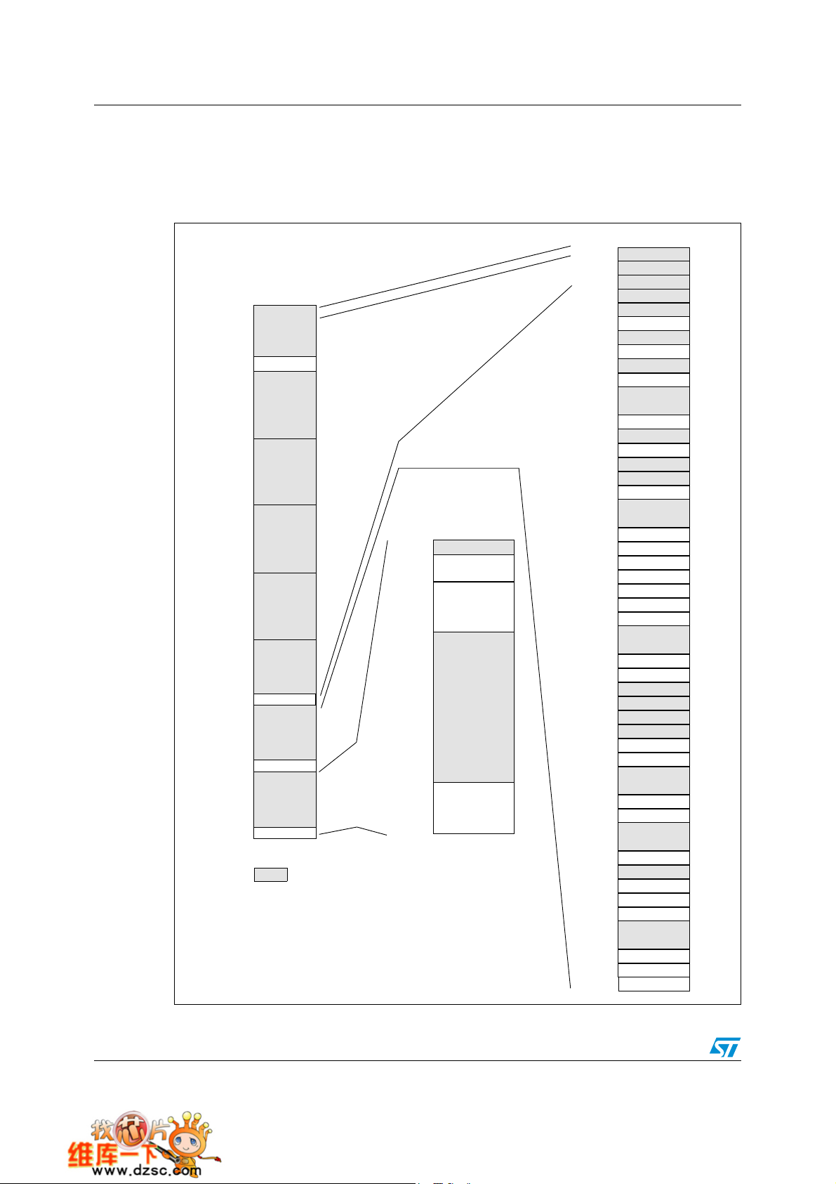
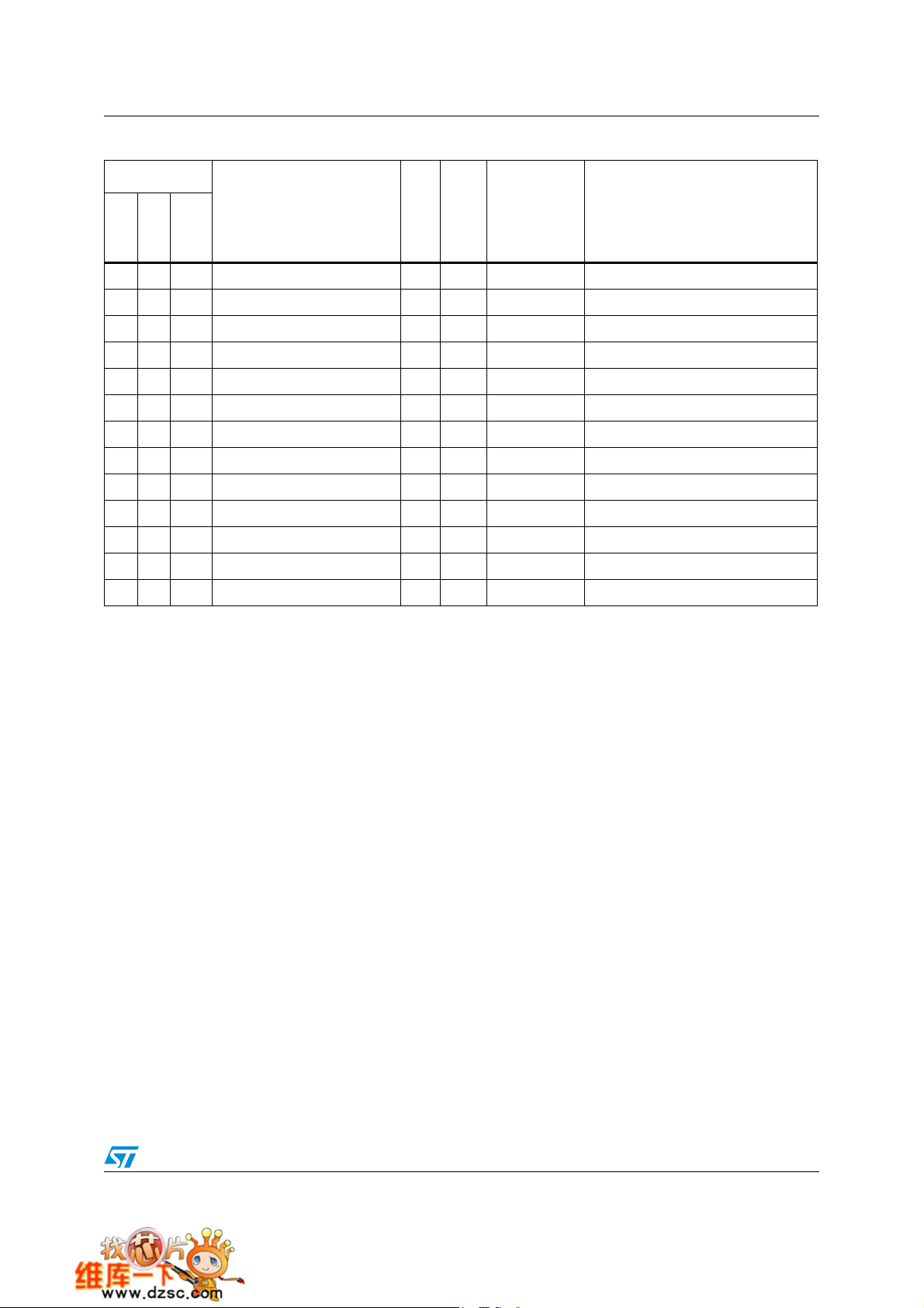
Memory mapping STM32F101xx
4 Memory mapping
The memory map is shown in Figure 5.
Figure 5. Memory map
APB memory space
0xFFFF FFFF
0xFFFF F000
7
0xE010 0000
0xE000 0000
6
0xC000 0000
5
0xA000 0000
4
0x8000 0000
3
0x6000 0000
2
0x4000 0000
1
0x2000 0000
0
0x0000 0000
ai14379
Cortex-M3 internal
peripherals
Peripherals
SRAM
Code
Reserved
0x1FFF FFFF
0x1FFF F9FF
0x1FFF F800
0x1FFF F000
0x0801 FFFF
0x0800 0000
reserved
Option bytes
System memory
reserved
Flash memory
0xFFFF FFFF
0xE010 0000
0x6000 0000
0x4002 3400
0x4002 3000
0x4002 2400
0x4002 2000
0x4002 1400
0x4002 1000
0x4002 0400
0x4002 0000
0x4001 3C00
0x4001 3800
0x4001 3400
0x4001 3000
0x4001 2C00
0x4001 2800
0x4001 2400
0x4001 1C00
0x4001 1800
0x4001 1400
0x4001 1000
0x4001 0C00
0x4001 0800
0x4001 0400
0x4001 0000
0x4000 7400
0x4000 7000
0x4000 6C00
0x4000 6800
0x4000 6400
0x4000 6000
0x4000 5C00
0x4000 5800
0x4000 5400
0x4000 4C00
0x4000 4800
0x4000 4400
0x4000 3C00
0x4000 3800
0x4000 3400
0x4000 3000
0x4000 2C00
0x4000 2800
0x4000 0C00
0x4000 0800
0x4000 0400
0x4000 0000
reserved
reserved
reserved
reserved
reserved
Flash interface
reserved
RCC
reserved
DMA
reserved
USART1
reserved
SPI1
reserved
reserved
ADC1
reserved
Port E
Port D
Port C
Port B
Port A
EXTI
AFIO
reserved
PWR
BKP
reserved
reserved
reserved
reserved
I2C2
I2C1
reserved
USART3
USART2
reserved
SPI2
reserved
IWDG
WWDG
RTC
reserved
TIM4
TIM3
TIM2
4K
1K
3K
1K
3K
1K
3K
1K
1K
1K
1K
1K
1K
1K
1K
2K
1K
1K
1K
1K
1K
1K
1K
35K
1K
1K
1K
1K
1K
1K
1K
1K
2K
1K
1K
2K
1K
1K
1K
1K
1K
7K
1K
1K
1K
20/64
 Loading...