

Datasheet ST72T213G1, ST72T212G2, ST72T101G2, ST72T101G1, ST72101G2 Datasheet (SGS Thomson Microelectronics)
...Page 1
September 1999 1/84
ST72101/ST72212/ST72213
8-BIT MCU WITH 4 TO 8K ROM/OTP/EPROM,
256 BYTES RAM, ADC, WDG, SPI AND 1 OR 2 TIMERS
DATASHEET
■ User Program Memory (ROM/OTP/EPROM):
4 to8K bytes
■ Data RAM: 256 bytes, including 64 bytes of
stack
■ Master Resetand Power-On Reset
■ Run, Wait, Slow, Halt and RAM Retention
modes
■ 22 multifunctionalbidirectional I/O lines:
– 22 programmable interrupt inputs
– 8 high sinkoutputs
– 6 analog alternateinputs
– 10 to 14 alternate functions
– EMI filtering
■ Programmable watchdog (WDG)
■ One or two 16-bit Timers, each featuring:
– 2 Input Captures
– 2 Output Compares
– External Clock input (on Timer A only)
– PWM and Pulse Generator modes
■ Synchronous Serial Peripheral Interface (SPI)
■ 8-bit Analog-to-Digital converter (6 channels)
(ST72212 and ST72213 only)
■ 8-bit Data Manipulation
■ 63 Basic Instructions
■ 17 mainAddressing Modes
■ 8 x8 Unsigned Multiply Instruction
■
True BitManipulation
■ Complete Development Support on PC/DOS-
WINDOWSTMReal-Time Emulator
■ Full Software Package on DOS/WINDOWS
TM
(C-Compiler, Cross-Assembler, Debugger)
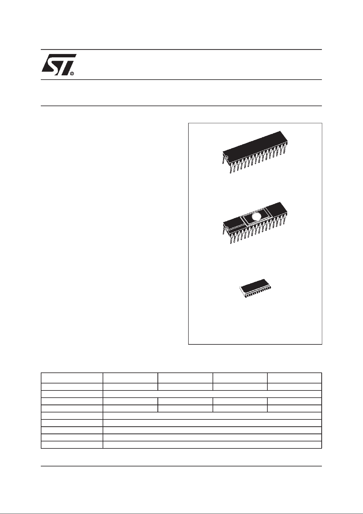
Device Summary
SO28
PSDIP32
CSDIP32W
(See ordering information at the end of datasheet)
Features ST72101G1 ST72101G2 ST72213G1 ST72212G2
Program Memory- bytes 4K 8K 4K 8K
RAM (stack) - bytes 256 (64)
16-bit Timers one one one two
ADC no no yes yes
Other Peripherals Watchdog, SPI
Operating Supply 3 to 5.5 V
CPU Frequency 8MHz max (16MHz oscillator) - 4MHz max over 85°C
Temperature Range - 40°C to + 125°C
Package SO28 - SDIP32
1
Rev. 1.7
Page 2

2/84
Table of Contents
95
1 GENERAL DESCRIPTION . . . . . . ................................................ 4
1.1 INTRODUCTION . . . . . . . . . . . . ............................................. 4
1.2 PIN DESCRIPTION . . ..................................................... 5
1.3 EXTERNAL CONNECTIONS . .. . . . . . . . . . . . . . . . . . . .. . . . . . . .. . . . . . . . . ......... 9
1.4 MEMORY MAP . . . . . .. . . . ............................................... 10
2 CENTRAL PROCESSING UNIT . . ............................................... 13
2.1 INTRODUCTION . . . . . . . . . . . . ............................................13
2.2 MAIN FEATURES . . . . . . . . . . . . . . . . . . . . . . . . . .............................. 13
2.3 CPU REGISTERS . . . .................................................... 13
3 CLOCKS, RESET, INTERRUPTS & POWER SAVING MODES . . . . . .. . . . . . . ...........16
3.1 CLOCK SYSTEM . . . . . .. . . . . . ............................................16
3.1.1 General Description . . . .. . ...........................................16
3.2 RESET . . . . . . . . . . . . .. . . . . . . .. . . . . . . . . . . . . .............................. 17
3.2.1 Introduction . . . .................................................... 17
3.2.2 External Reset . . . . . . ...............................................17
3.2.3 Reset Operation . . . . . . . . . . . . . . . . . . . . . . . . . ........................... 17
3.2.4 Power-on Reset .................................................... 17
3.3 INTERRUPTS . . . .. . . . . . .. . . . . . . . . . . . . . . . . . . . . .. . . . . . . . . .. . . . . . . .. . . . . . . 18
3.4 POWER SAVING MODES . .. . . . . . . . . . . . . . . . . . . . . .. . . . . . . . . .. . . . . . . ........ 21
3.4.1 Introduction . . . .................................................... 21
3.4.2 Slow Mode . . .. . . . . . . . . . . . . . . . . . . . ................................. 21
3.4.3 Wait Mode . . . . . . . . . . . . . . .. ........................................ 21
3.4.4 Halt Mode . . . . . .................................................... 22
3.5 MISCELLANEOUS REGISTER . . . . .. . . . . . .................................. 23
4 ON-CHIP PERIPHERALS . . . . . . . . . . . ...........................................24
4.1 I/O PORTS . . . . . . . . .. . . . . . . . . ...........................................24
4.1.1 Introduction . . . .................................................... 24
4.1.2 Functional Description . . . . ...........................................24
4.1.3 I/O Port Implementation . . . . . . . . . . . . . . . . . . . ........................... 25
4.1.4 Register Description . . . . . . ...........................................28
4.2 WATCHDOG TIMER (WDG) . . . . . . .. . . . . . . .. . . .. . . .. . . . . . . . . . . . . . . . .. . . . . . . 30
4.2.1 Introduction . . . .................................................... 30
4.2.2 Main Features . .. . . . ...............................................30
4.2.3 Functional Description . . . . ...........................................31
4.2.4 Low Power Modes . . . ............................................... 31
4.2.5 Interrupts . . . . . .. . . . . . . . . . .. . . . . . . ................................. 31
4.2.6 Register Description . . . . . . ...........................................31
4.3 16-BIT TIMER . . . . . . . . . . . . . . . . . . ........................................32
4.3.1 Introduction . . . .................................................... 32
4.3.2 Main Features . .. . . . ...............................................32
4.3.3 Functional Description . . . . ...........................................32
4.3.4 Low Power Modes . . ............................................... 43
4.3.5 Interrupts . . .. . .................................................... 43
4.3.6 Register Description . . . . . . ...........................................44
2
Page 3

3/84
Table of Contents
4.4 SERIAL PERIPHERAL INTERFACE (SPI) . . . . . . . . . . . . . . . .. . . . . . . . . ...........49
4.4.1 Introduction . . . .................................................... 49
4.4.2 Main Features . .. . . . ...............................................49
4.4.3 General description . . . . . .. . . . . . . . .. . . .. . . . . . . . . . .. . . . . . . . . . . . . . . . . . . 49
4.4.4 Functional Description . . . . ...........................................51
4.4.5 Low Power Modes . . . ............................................... 58
4.4.6 Interrupts . . .. . .................................................... 58
4.4.7 Register Description . . . . . . ...........................................59
4.5 8-BIT A/D CONVERTER (ADC) . . . . . .. . . . . . . . . . . . ........................... 62
4.5.1 Introduction . . . .................................................... 62
4.5.2 Main Features . .. . . . ...............................................62
4.5.3 Functional Description . . . . ...........................................63
4.5.4 Low Power Modes . . . ............................................... 63
4.5.5 Interrupts . . . . . .. . . . . . . . . . .. . . . . . . ................................. 63
4.5.6 Register Description . . . . . . ...........................................64
5 INSTRUCTION SET . . . . . . . . . . . . . . . . . . ........................................ 65
5.1 ST7 ADDRESSING MODES . . . . . . . . . . . . . . .. . . . . . . . . . . . . . . . . . . .. . . . . . . . . . . . 65
5.1.1 Inherent . . . . . . . . . . . ...............................................66
5.1.2 Immediate . .. . . . . . . . . . . . . . . . . . . .. . . .. . . . . . . . . . . . . . . . . . . . . . . . . . . . . . 66
5.1.3 Direct . ........................................................... 66
5.1.4 Indexed (No Offset, Short, Long) . . . . . . . . . . . . ........................... 66
5.1.5 Indirect (Short, Long) . . . . .. . . . . . . . . . .. . . . . . . . . . . . .. . . .. . . . . . . . . . . . . . . 66
5.1.6 Indirect Indexed (Short,Long) . ........................................67
5.1.7 Relative mode (Direct,Indirect) . . . .. . . . . . . . . . . . . . . . . . . . . . . .. . . .. . . . . . . . 67
5.2 INSTRUCTION GROUPS . . . . . . . . . . . . . . . . ................................. 68
6 ELECTRICALCHARACTERISTICS . . . . . . . . . . . . . . . . .............................. 71
6.1 ABSOLUTE MAXIMUM RATINGS . . . ........................................71
6.2 RECOMMENDED OPERATING CONDITIONS . . ............................... 72
6.3 DC ELECTRICAL CHARACTERISTICS . . . . . . . . . . . . . .. . . . . . . . . . . . . ...........73
6.4 RESET CHARACTERISTICS . . . . . . . . . ..................................... 74
6.5 OSCILLATOR CHARACTERISTICS . . . .. . . . . . . .............................. 74
6.6 A/D CONVERTERCHARACTERISTICS (ST72212 AND ST72213ONLY) . . . ........ 75
6.7 SPI CHARACTERISTICS . . ...............................................77
7 GENERAL INFORMATION . . . . . . . . . . ........................................... 80
7.1 EPROM ERASURE . . .. . . . . . . . . . . . . .. . . . . . ............................... 80
7.2 PACKAGE MECHANICALDATA . . . . . . . . . . . . .. . . . ........................... 80
7.3 ORDERING INFORMATION . . . . . .. . . . . . . .................................. 82
7.3.1 Transfer Of CustomerCode . . . . . . . . . . . .. . . .. . . . . . . . . . . . ............... 82
8 SUMMARY OF CHANGES . . . . . . . . . . . . . . . . . . . . . . . . .. . . . . . . . . . . . . . . . . . . . . . . . . . . . 84
3
Page 4
4/84
ST72101/ST72212/ST72213
1 GENERAL DESCRIPTION
1.1 INTRODUCTION
The ST72101, ST72213 and ST72212 HCMOS
Microcontroller Units are members of the ST7
family. These devices are based on an industrystandard 8-bit core and feature an enhanced
instruction set. They normally operate ata 16MHz
oscillator frequency. Under software control, the
ST72101, ST72213 and ST72212 may be placed
in either WAIT, SLOW or HALT modes, thus
reducing power consumption. The enhanced
instruction set and addressing modes afford real
programming potential. In addition to standard
8-bit data management, the ST72101, ST72213
and ST72212 feature true bit manipulation, 8x8
unsigned multiplication and indirect addressing
modes on the whole memory. The devices include
an on-chip oscillator, CPU, program memory
(ROM/OTP/EPROM versions), RAM, 22 I/O lines
and the following on-chip peripherals: Analog-toDigital Converter (ADC) with 6 multiplexed analog
inputs (ST72212 and ST72213 only), industry
standard synchronous SPI serial interface, digital
Watchdog, one or two independent 16-bit Timers,
one featuring an External Clock Input, and both
featuring Pulse Generator capabilities, 2 Input
Captures and 2 Output Compares.
Figure 1. ST72101, ST72213 and ST72212 Block Diagram
8-BIT CORE
ALU
ADDRESSAND DATA BUS
OSCIN
OSCOUT
RESET
PORT B
TIMER A
PORT A
SPI
PORT C
8-BIT ADC
1)
WATCHDOG
PB0 -> PB7
(8 bits)
PC0 -> PC5
(6 bits)
OSC
Internal
CLOCK
CONTROL
RAM
(256 Bytes)
PA0 -> PA7
(8 bits)
V
SS
V
DD
POWER
SUPPLY
TIMER B
2)
1) ST72213 and ST72212 only
2) ST72212 only
PROGRAM
(4 - 8K Bytes)
MEMORY
4
Page 5
5/84
ST72101/ST72212/ST72213
1.2 PIN DESCRIPTION
Figure 2. ST72212 Pinout (SO28)
Figure 3. ST72213 Pinout (SO28)
Figure 4. ST72101 Pinout (SO28)
Figure 5. ST72212 Pinout (SDIP32)
Figure 6. ST72213 Pinout (SDIP32)
Figure 7. ST72101 Pinout (SDIP32)
V
DD
V
SS
TEST/V
PP
1)
PA0
PA1
PA2
PA3
PA4
PA5
PA6
PA7
PC0/ICAP1_B/AIN0
PC1/OCMP1_B/AIN1
PC2/CLKOUT/AIN2
RESET
OSCIN
OSCOUT
SS/PB7
SCK/PB6
MISO/PB5
MOSI/PB4
OCMP2_A/PB3
ICAP2_A/PB2
OCMP1_A/PB1
ICAP1_A/PB0
AIN5/EXTCLK_A/PC5
AIN4/OCMP2_B/PC4
AIN3/ICAP2_B/PC3
15
16
17
18
19
20
28
27
26
25
24
23
22
21
1
2
3
4
5
6
7
8
9
10
11
12
13
14
1) VPPonEPROM/OTP only
V
DD
V
SS
TEST/V
PP
1)
PA0
PA1
PA2
PA3
PA4
PA5
PA6
PA7
PC0/AIN0
PC1/AIN1
PC2/CLKOUT/AIN2
RESET
OSCIN
OSCOUT
SS/PB7
SCK/PB6
MISO/PB5
MOSI/PB4
OCMP2_A/PB3
ICAP2_A/PB2
OCMP1_A/PB1
ICAP1_A/PB0
AIN5/EXTCLK_A/PC5
AIN4/PC4
AIN3/PC3
15
16
17
18
19
20
28
27
26
25
24
23
22
21
1
2
3
4
5
6
7
8
9
10
11
12
13
14
1) VPPon EPROM/OTPonly
V
DD
V
SS
TEST/V
PP
1)
PA0
PA1
PA2
PA3
PA4
PA5
PA6
PA7
PC0
PC1
PC2/CLKOUT
RESET
OSCIN
OSCOUT
SS/PB7
SCK/PB6
MISO/PB5
MOSI/PB4
OCMP2_A/PB3
ICAP2_A/PB2
OCMP1_A/PB1
ICAP1_A/PB0
EXTCLK_A/PC5
PC4
PC3
15
16
17
18
19
20
28
27
26
25
24
23
22
21
1
2
3
4
5
6
7
8
9
10
11
12
13
14
1) VPPon EPROM/OTP only
RESET
OSCIN
OSCOUT
SS/PB7
SCK/PB6
MISO/PB5
MOSI/PB4
OCMP2_A/PB3
ICAP2_A/PB2
OCMP1_A/PB1
ICAP1_A/PB0
AIN5/EXTCLK_A/PC5
AIN4/OCMP2_B/PC4
AIN3/ICAP2_B/PC3
V
DD
V
SS
TEST/V
PP
1)
PA0
PA1
PA2
PA3
PA4
PA5
PA6
PA7
PC0/ICAP1_B/AIN0
PC1/OCMP1_B/AIN1
PC2/CLKOUT/AIN2
NC
NC
NC
NC
28
27
26
25
24
23
22
21
20
19
18
17
16
15
1
2
3
4
5
6
7
8
9
10
11
12
13
14
29
30
31
32
1) VPPon EPROM/OTP only
RESET
OSCIN
OSCOUT
SS/PB7
SCK/PB6
MISO/PB5
MOSI/PB4
OCMP2_A/PB3
ICAP2_A/PB2
OCMP1_A/PB1
ICAP1_A/PB0
AIN5/EXTCLK_A/PC5
AIN4/PC4
AIN3/PC3
NC
NC
V
DD
V
SS
TEST/V
PP
1)
PA0
PA1
PA2
PA3
PA4
PA5
PA6
PA7
PC0/AIN0
PC1/AIN1
PC2/CLKOUT/AIN2
NC
NC
28
27
26
25
24
23
22
21
20
19
18
1716
15
1
2
3
4
5
6
7
8
9
10
11
12
13
14
29
30
31
32
1) VPPonEPROM/OTP only
V
DD
V
SS
TEST/V
PP
1)
PA0
PA1
PA2
PA3
PA4
PA5
PA6
PA7
PC0
PC1
PC2/CLKOUT
RESET
OSCIN
OSCOUT
SS/PB7
SCK/PB6
MISO/PB5
MOSI/PB4
OCMP2_A/PB3
ICAP2_A/PB2
OCMP1_A/PB1
ICAP1_A/PB0
EXTCLK_A/PC5
PC4
PC3
NC
NC
NC
NC
28
27
26
25
24
23
22
21
20
19
18
1716
15
1
2
3
4
5
6
7
8
9
10
11
12
13
14
29
30
31
32
1) VPPon EPROM/OTPonly
5
Page 6
6/84
ST72101/ST72212/ST72213
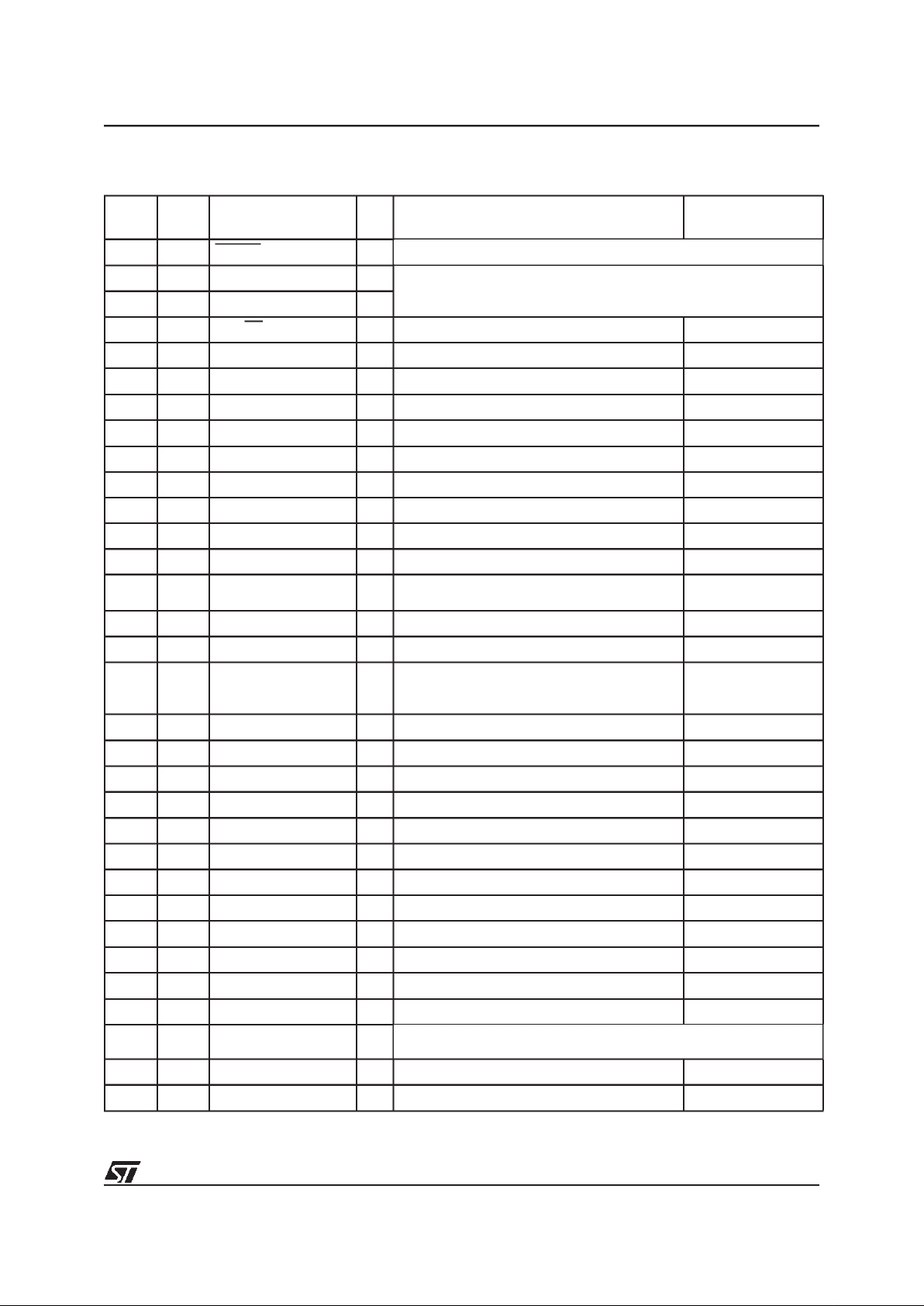
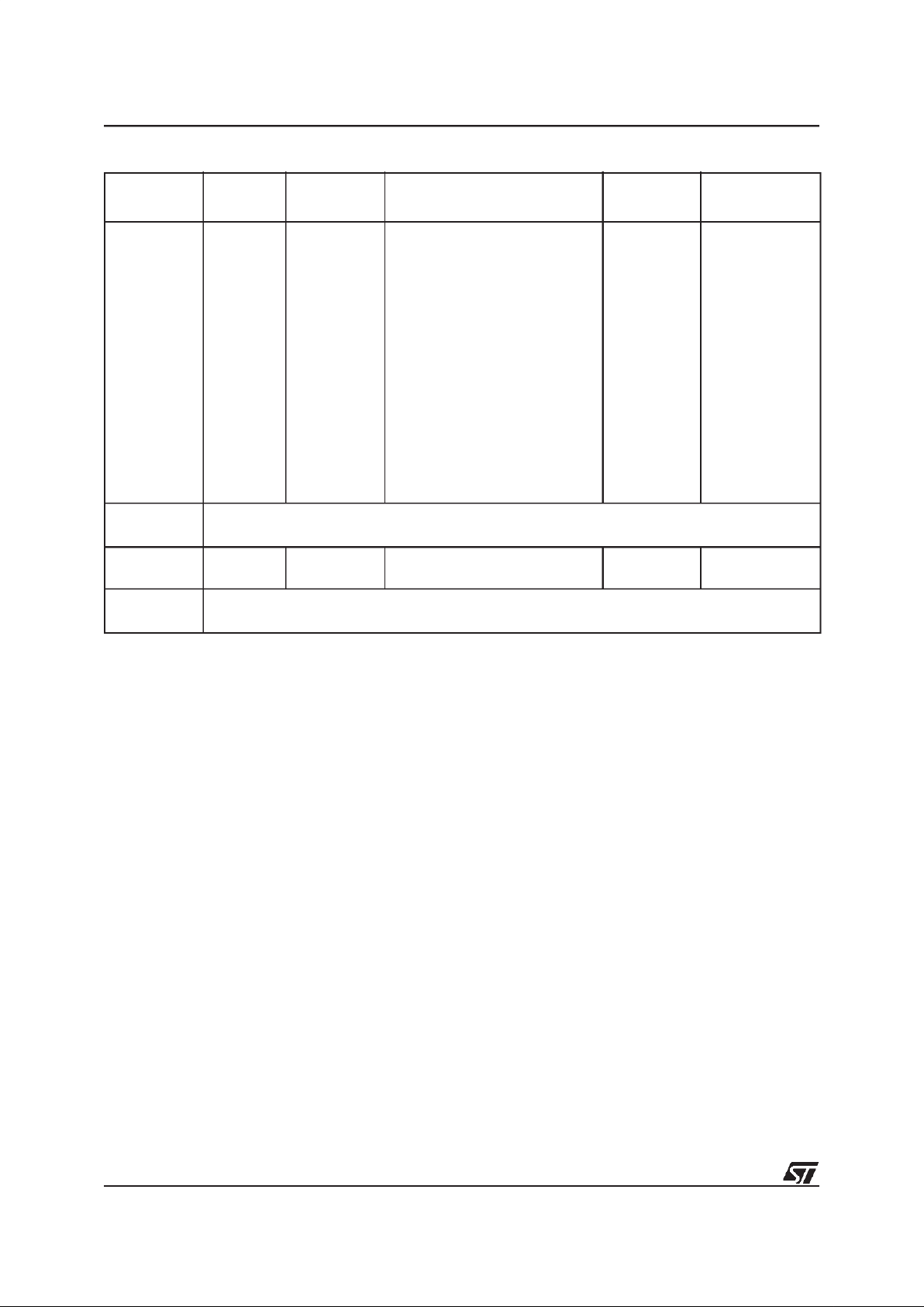
Table 1. ST72212 Pin Configuration
Note 1:VPPon EPROM/OTP only
Pin n°
SDIP32
Pin n °
SO28
Pin Name Type Description Remarks
1 1 RESET I/O Bidirectional. Active low. Top priority non maskable interrupt.
22OSCIN I
Input/Output Oscillator pin. These pins connect a parallel-resonant
crystal, or an external source to the on-chip oscillator.
3 3 OSCOUT O
4 4 PB7/SS I/O Port B7 or SPI Slave Select (active low) External Interrupt: EI1
5 5 PB6/SCK I/O Port B6 or SPI Serial Clock External Interrupt: EI1
6 6 PB5/MISO I/O Port B5 or SPI Master In/ Slave Out Data External Interrupt: EI1
7 7 PB4/MOSI I/O Port B4 or SPI Master Out / Slave In Data External Interrupt: EI1
8 NC Not Connected
9 NC Not Connected
10 8 PB3/OCMP2_A I/O Port B3 or TimerA Output Compare 2 External Interrupt: EI1
11 9 PB2/ICAP2_A I/O Port B2 or TimerA Input Capture 2 External Interrupt: EI1
12 10 PB1/OCMP1_A I/O Port B1 or TimerA Output Compare 1 External Interrupt: EI1
13 11 PB0/ICAP1_A I/O Port B0 or TimerA Input Capture 1 External Interrupt: EI1
14 12 PC5/EXTCLK_A/AIN5 I/O PortC5orTimerA InputClockorADCAnalog Input5 External Interrupt: EI1
15 13 PC4/OCMP2_B/AIN4 I/O
PortC4orTimerB OutputCompare2orADCAnalog
Input 4
External Interrupt: EI1
16 14 PC3 /IC A P2 _ B /AIN 3 I/O
Port C3 orTimerB InputCapture 2 orADC Analog
Input 3
External Interrupt: EI1
17 15 PC2/CLKOUT/AIN2 I/O
Port C2or InternalClockFrequency Outputor ADC
Analog Input 2. Clockout is driven by Bit 5 of the
miscellaneous register.
External Interrupt: EI1
18 16 PC1/OCMP1_B/AIN1 I/O
PortC1orTimerB OutputCompare1orADCAnalog
Input 1
External Interrupt: EI1
19 17 PC0 /IC A P1 _ B /AIN 0 I/O
Port C0 orTimerB InputCapture 1 orADC Analog
Input 0
External Interrupt: EI1
20 18 PA7 I/O Port A7, High Sink External Interrupt: EI0
21 19 PA6 I/O Port A6, High Sink External Interrupt: EI0
22 20 PA5 I/O Port A5, High Sink External Interrupt: EI0
23 21 PA4 I/O Port A4, High Sink External Interrupt: EI0
24 NC Not Connected
25 NC Not Connected
26 22 PA3 I/O Port A3, High Sink External Interrupt: EI0
27 23 PA2 I/O Port A2, High Sink External Interrupt: EI0
28 24 PA1 I/O Port A1, High Sink External Interrupt: EI0
29 25 PA0 I/O Port A0, High Sink External Interrupt: EI0
30 26 TEST/V
PP
(1)
I/S
Test mode pin (should be tied low in user mode). In the EPROM programming mode, this pin acts as the programming voltage input V
PP.
31 27 V
SS
S Ground
32 28 V
DD
S Main power supply
6
Page 7
7/84
ST72101/ST72212/ST72213
Table 2. ST72213 Pin Configuration
Note 1:VPPon EPROM/OTP only
Pin n°
SDIP32
Pin n°
SO28
Pin Name Type Description Remarks
1 1 RESET I/O
Bidirectional. Active low. Top priority non maskable interrupt.
2 2 OSCIN I
Input/Output Oscillator pin. These pins connect a parallel-resonant
crystal, oran external source to the on-chip oscillator.
3 3 OSCOUT O
4 4 PB7/SS I/O Port B7 orSPI Slave Select (active low) External Interrupt: EI1
5 5 PB6/SCK I/O Port B6 orSPI Serial Clock External Interrupt: EI1
6 6 PB5/MISO I/O Port B5 orSPI Master In/ Slave Out Data External Interrupt: EI1
7 7 PB4/MOSI I/O Port B4 orSPI Master Out / Slave In Data External Interrupt: EI1
8 NC Not Connected
9 NC Not Connected
10 8 PB3/OCMP2_A I/O Port B3 or TimerA Output Compare 2 External Interrupt: EI1
11 9 PB2/ICAP2_A I/O Port B2 orTimerA Input Capture 2 External Interrupt: EI1
12 10 PB1/OCMP1_A I/O Port B1 or TimerA Output Compare 1 External Interrupt: EI1
13 11 PB0/ICAP1_A I/O Port B0 orTimerA Input Capture 1 External Interrupt: EI1
14 12 PC5/EXTCLK_A/AIN5 I/O
Port C5 orTimerA Input Clock or ADC Analog
Input 5
External Interrupt: EI1
15 13 PC4/AIN4 I/O Port C4 or ADC Analog Input 4 External Interrupt: EI1
16 14 PC3/AIN3 I/O Port C3 or ADC Analog Input 3 External Interrupt: EI1
17 15 PC2/CLKOUT/AIN2 I/O
Port C2 orInternal Clock Frequency Output or
ADC Analog Input 2. Clockout is driven by Bit 5
of the miscellaneous register.
External Interrupt: EI1
18 16 PC1/AIN1 I/O Port C1 or ADC Analog Input 1 External Interrupt: EI1
19 17 PC0/AIN0 I/O Port C0 or ADC Analog Input 0 External Interrupt: EI1
20 18 PA7 I/O Port A7, High Sink External Interrupt: EI0
21 19 PA6 I/O Port A6, High Sink External Interrupt: EI0
22 20 PA5 I/O Port A5, High Sink External Interrupt: EI0
23 21 PA4 I/O Port A4, High Sink External Interrupt: EI0
24 NC Not Connected
25 NC Not Connected
26 22 PA3 I/O Port A3, High Sink External Interrupt: EI0
27 23 PA2 I/O Port A2, High Sink External Interrupt: EI0
28 24 PA1 I/O Port A1, High Sink External Interrupt: EI0
29 25 PA0 I/O Port A0, High Sink External Interrupt: EI0
30 26 TEST/V
PP
(1)
I/S
Test mode pin (should be tied low in user mode). In the EPROM programming mode, this pin acts asthe programming voltage input V
PP.
31 27 V
SS
S Ground
32 28 V
DD
S Main power supply
7
Page 8

8/84
ST72101/ST72212/ST72213
Table 3. ST72101 Pin Configuration
Pin n°
SDIP32
Pinn°
SO28
Pin Name Type Description Remarks
1 1 RESET I/O Bidirectional. Active low. Top priority non maskable interrupt.
2 2 OSCIN I
Input/Output Oscillator pin. These pins connect a parallel-resonant crystal, or
an external source to the on-chip oscillator.
3 3 OSCOUT O
4 4 PB7/SS I/O Port B7 orSPI Slave Select (active low) External Interrupt: EI1
5 5 PB6/SCK I/O Port B6 orSPI Serial Clock External Interrupt: EI1
6 6 PB5/MISO I/O Port B5 orSPI Master In/ Slave Out Data External Interrupt: EI1
7 7 PB4/MOSI I/O Port B4 orSPI Master Out / Slave In Data External Interrupt: EI1
8 NC Not Connected
9 NC Not Connected
10 8 PB3/OCMP2_A I/O Port B3 orTimerA Output Compare 2 External Interrupt: EI1
11 9 PB2/ICAP2_A I/O Port B2 orTimerA Input Capture 2 External Interrupt: EI1
12 10 PB1/OCMP1_A I/O Port B1 orTimerA Output Compare 1 External Interrupt: EI1
13 11 PB0/ICAP1_A I/O Port B0 orTimerA Input Capture 1 External Interrupt: EI1
14 12 PC5/EXTCLK_A I/O Port C5 or TimerA Input Clock External Interrupt: EI1
15 13 PC4 I/O Port C4 External Interrupt: EI1
16 14 PC3 I/O Port C3 External Interrupt: EI1
17 15 PC2/CLKOUT I/O
Port C2 or Internal Clock Frequency Output.Clockout
is driven by MCO bit of the miscellaneous register.
External Interrupt: EI1
18 16 PC1 I/O Port C1 External Interrupt: EI1
19 17 PC0 I/O Port C0 External Interrupt: EI1
20 18 PA7 I/O Port A7, High Sink External Interrupt: EI0
21 19 PA6 I/O Port A6, High Sink External Interrupt: EI0
22 20 PA5 I/O Port A5, High Sink External Interrupt: EI0
23 21 PA4 I/O Port A4, High Sink External Interrupt: EI0
24 NC Not Connected
25 NC Not Connected
26 22 PA3 I/O Port A3, High Sink External Interrupt: EI0
27 23 PA2 I/O Port A2, High Sink External Interrupt: EI0
28 24 PA1 I/O Port A1, High Sink External Interrupt: EI0
29 25 PA0 I/O Port A0, High Sink External Interrupt: EI0
30 26 TEST/V
PP
(1)
I/S
Test mode pin (should be tied low in user mode). In the EPROM programming
mode, this pin acts as the programming voltage input V
PP.
31 27 V
SS
S Ground
32 28 V
DD
S Main power supply
Note 1:V
PP
on EPROM/OTP only.
8
Page 9
9/84
ST72101/ST72212/ST72213
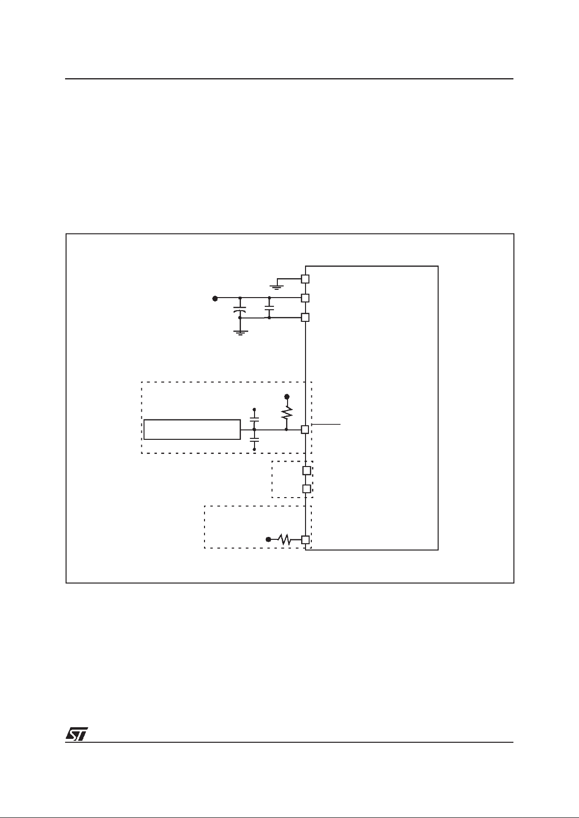
1.3 EXTERNAL CONNECTIONS
The following figure shows the recommended external connections for the device.
The VPPpin is only used for programming OTP
and EPROM devices and must betied to ground in
user mode.
The 10 nF and 0.1 µF decoupling capacitors on
the power supply lines are a suggested EMC performance/cost tradeoff.
The external reset network is intended to protect
the device against parasitic resets, especially in
noisy environments.
Unused I/Os should be tied high to avoid any unnecessary power consumption on floating lines.
An alternative solution is to program the unused
ports as inputs with pull-up.
Figure 8. Recommended External Connections
V
PP
V
DD
V
SS
OSCIN
OSCOUT
RESET
V
DD
0.1µF
+
See
Clocks
Section
V
DD
0.1µF
0.1µF
EXTERNAL RESET CIRCUIT
Or configure unused I/O ports
Unused I/O
10nF
4.7K
10K
by software as input with pull-up
V
DD
9
Page 10
10/84
ST72101/ST72212/ST72213
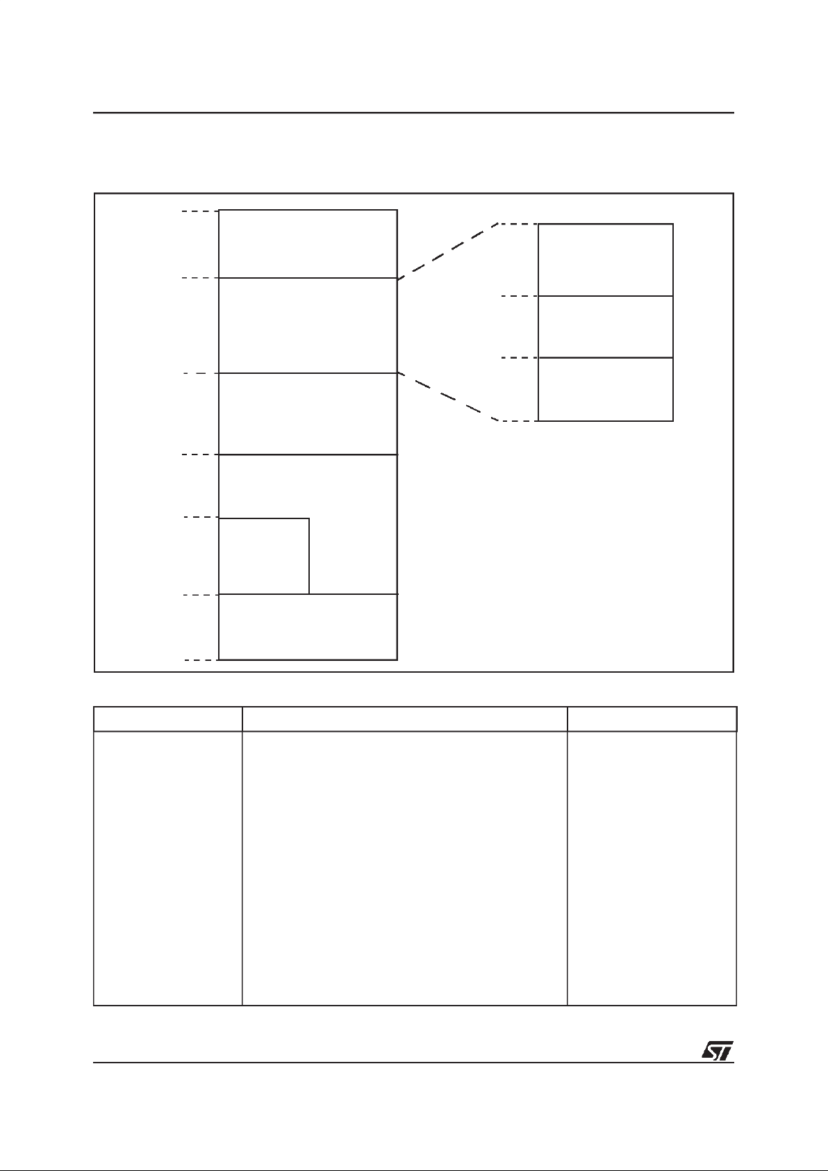
1.4 MEMORY MAP
Figure 9. Memory Map
Table 4. Interrupt Vector Map
Vector Address Description Remarks
FFE0-FFE1h
FFE2-FFE3h
FFE4-FFE5h
FFE6-FFE7h
FFE8-FFE9h
FFEA-FFEBh
FFEC-FFEDh
FFEE-FFEFh
FFF0-FFF1h
FFF2-FFF3h
FFF4-FFF5h
FFF6-FFF7h
FFF8-FFF9h
FFFA-FFFBh
FFFC-FFFDh
FFFE-FFFFh
Not Used
Not Used
Not Used
Not Used
Not Used
Not Used
Not Used
TIMER B Interrupt Vector (ST72212 only)
Not Used
TIMER A Interrupt Vector
SPI Interrupt Vector
Not Used
External Interrupt Vector EI1
External Interrupt Vector EI0
TRAP (software) Interrupt Vector
RESET Vector
Internal Interrupt
Internal Interrupt
Internal Interrupt
External Interrupt
External Interrupt
CPU Interrupt
0000h
8K Bytes
Interrupt & Reset Vectors
HW Registers
017Fh
0080h
007Fh
DFFFh
Reserved
(see Table 5)
E000h
FFDFh
FFE0h
FFFFh
(see Table 4)
4K Bytes
F000h
256 Bytes RAM
Short Addressing
RAM (zero page)
16-bit Addressing
RAM
0100h
0140h
017Fh
0080h
00FFh
013Fh
64 Bytes Stack or
16-bit Addressing RAM
0180h
Program Memory
Program
Memory
10
Page 11
11/84
ST72101/ST72212/ST72213
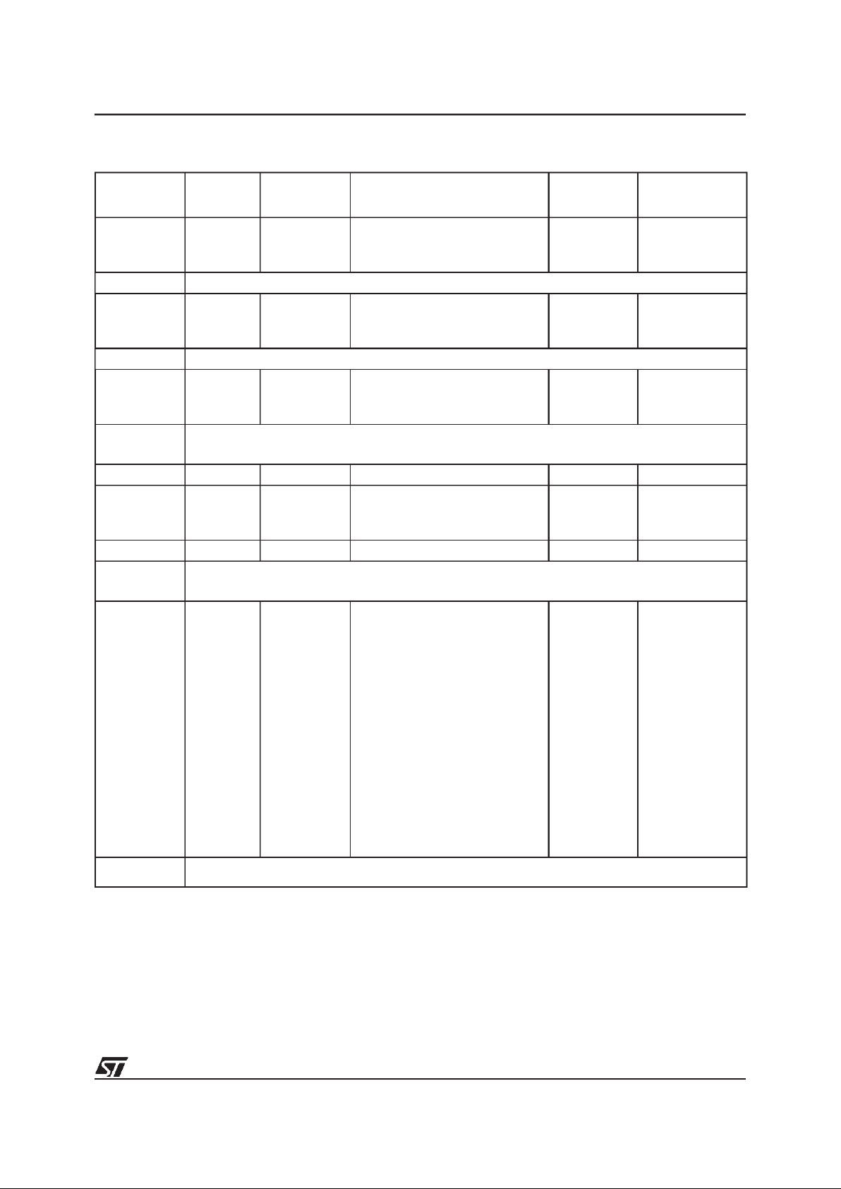
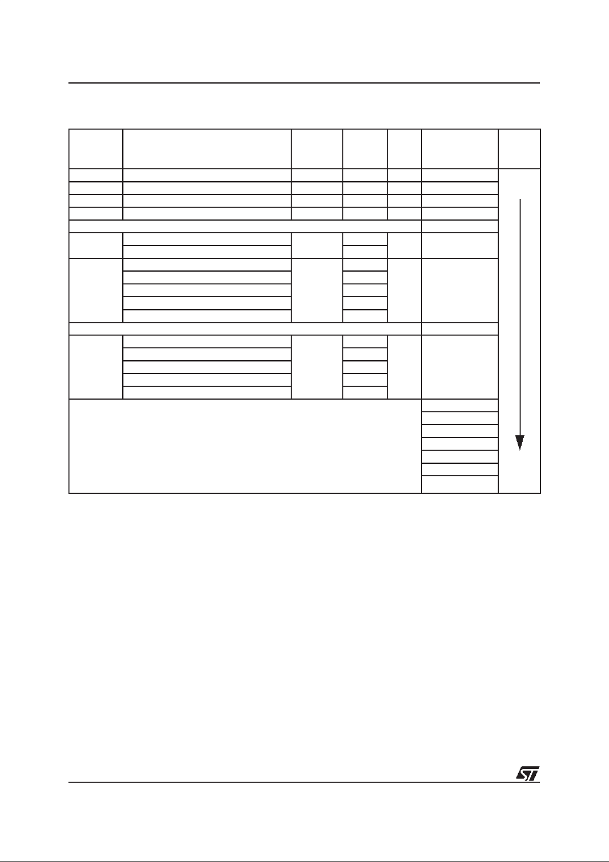
Table 5. Hardware Register Memory Map
Address
Block
Name
Register
Label
Register name Reset Status Remarks
0000h
0001h
0002h
Port C
PCDR
PCDDR
PCOR
Data Register
Data Direction Register
Option Register
00h
00h
00h
R/W
R/W
R/W
0003h Reserved Area (1 Byte)
0004h
0005h
0006h
Port B
PBDR
PBDDR
PBOR
Data Register
Data Direction Register
Option Register
00h
00h
00h
R/W
R/W
R/W
0007h Reserved Area (1 Byte)
0008h
0009h
000Ah
Port A
PADR
PADDR
PAOR
Data Register
Data Direction Register
Option Register
00h
00h
00h
R/W
R/W
R/W
000Bh to
001Fh
Reserved Area (21 Bytes)
0020h MISCR Miscellaneous Register 00h R/W
0021h
0022h
0023h
SPI
SPIDR
SPICR
SPISR
Data I/O Register
Control Register
Status Register
xxh
0xh
00h
R/W
R/W
Read Only
0024h WDG WDGCR Watchdog Control register 7Fh R/W
0025h to
0030h
Reserved Area (12 Bytes)
0031h
0032h
0033h
0034h-0035h
0036h-0037h
0038h-0039h
003Ah-003Bh
003Ch-003Dh
003Eh-003Fh
Timer A
TACR2
TACR1
TASR
TAIC1HR
TAIC1LR
TAOC1HR
TAOC1LR
TACHR
TACLR
TAACHR
TAACLR
TAIC2HR
TAIC2LR
TAOC2HR
TAOC2LR
Control Register2
Control Register1
Status Register
Input Capture1 High Register
Input Capture1 Low Register
Output Compare1 High Register
Output Compare1 Low Register
Counter High Register
Counter Low Register
Alternate Counter High Register
Alternate Counter Low Register
Input Capture2 High Register
Input Capture2 Low Register
Output Compare2 High Register
Output Compare2 Low Register
00h
00h
00h
xxh
xxh
80h
00h
FFh
FCh
FFh
FCh
xxh
xxh
80h
00h
R/W
R/W
Read Only
Read Only
Read Only
R/W
R/W
Read Only
Read Only
Read Only
Read Only
Read Only
Read Only
R/W
R/W
0040h Reserved Area (1 Byte)
11
Page 12
12/84
ST72101/ST72212/ST72213
Notes:
1. ST72212 only, reserved area for other devices.
2. ST72212 and ST72213 only, reserved otherwise.
0041h
0042h
0043h
0044h-0045h
0046h-0047h
0048h-0049h
004Ah-004Bh
004Ch-004Dh
004Eh-004Fh
Timer B
1)
TBCR2
TBCR1
TBSR
TBIC1HR
TBIC1LR
TBOC1HR
TBOC1LR
TBCHR
TBCLR
TBACHR
TBACLR
TBIC2HR
TBIC2LR
TBOC2HR
TBOC2LR
Control Register2
Control Register1
Status Register
Input Capture1 High Register
Input Capture1 Low Register
Output Compare1 High Register
Output Compare1 Low Register
Counter High Register
Counter Low Register
Alternate Counter High Register
Alternate Counter Low Register
Input Capture2 High Register
Input Capture2 Low Register
Output Compare2 High Register
Output Compare2 Low Register
00h
00h
00h
xxh
xxh
80h
00h
FFh
FCh
FFh
FCh
xxh
xxh
80h
00h
R/W
R/W
Read Only
Read Only
Read Only
R/W
R/W
Read Only
Read Only
Read Only
Read Only
Read Only
Read Only
R/W
R/W
0050h to
006Fh
Reserved Area (32 Bytes)
0070h
0071h
ADC
2)
ADCDR
ADCCSR
Data Register
Control/Status Register
00h
00h
Read Only
R/W
0072h to
007Fh
Reserved Area (14 Bytes)
Address
Block
Name
Register
Label
Register name Reset Status Remarks
12
Page 13
13/84
ST72101/ST72212/ST72213
2 CENTRAL PROCESSING UNIT
2.1 INTRODUCTION
This CPU hasa full 8-bit architecture andcontains
six internal registers allowing efficient 8-bit data
manipulation.
2.2 MAIN FEATURES
■ 63 basicinstructions
■ Fast 8-bit by 8-bit multiply
■ 17 main addressing modes (with indirect
addressing mode)
■ Two 8-bit index registers
■ 16-bit stackpointer
■ 8 MHzCPU internal frequency
■ Low power modes
■ Maskable hardware interrupts
■ Non-maskable software interrupt
2.3 CPU REGISTERS
The 6 CPU registers shown in Figure 10 are not
present in thememory mapping and are accessed
by specificinstructions.
Accumulator (A)
The Accumulator is an 8-bit general purpose register used to hold operands and the results of the
arithmetic and logic calculations andto manipulate
data.
Index Registers (Xand Y)
In indexedaddressingmodes, these 8-bit registers
are used to create either effective addresses or
temporary storage areas for data manipulation.
(The Cross-Assembler generates a precede instruction (PRE) to indicate that the following instruction refers to the Y register.)
The Y register is notaffected by theinterrupt automatic procedures (notpushed toand popped from
the stack).
Program Counter (PC)
The program counteris a16-bit register containing
the address of the next instruction to be executed
by the CPU. It is made of two 8-bit registers PCL
(Program CounterLow whichis the LSB) and PCH
(Program Counter High which is the MSB).
Figure 10. CPU Registers
ACCUMULATOR
X INDEX REGISTER
Y INDEX REGISTER
STACK POINTER
CONDITION CODE REGISTER
PROGRAM COUNTER
70
1C11HINZ
RESET VALUE= RESET VECTOR @ FFFEh-FFFFh
70
70
70
0
7
15 8
PCH
PCL
15
87 0
RESET VALUE = STACKHIGHER ADDRESS
RESET VALUE =
1X11X1XX
RESET VALUE = XXh
RESET VALUE= XXh
RESET VALUE = XXh
X = Undefined Value
13
Page 14

14/84
ST72101/ST72212/ST72213
CENTRAL PROCESSING UNIT (Cont’d)
CONDITION CODE REGISTER (CC)
Read/Write
Reset Value: 111x1xxx
The 8-bit Condition Code register contains the interrupt mask and four flags representative of the
result of the instructionjust executed. This register
can also be handled by the PUSH and POP instructions.
These bits can be individually tested and/or controlled by specific instructions.
Bit 4 = H
Half carry
.
This bit isset byhardware when a carry occurs between bits 3 and 4 of the ALU during an ADD or
ADC instruction.Itis reset by hardware during the
same instructions.
0: No half carry has occurred.
1: A half carry has occurred.
This bit is tested using the JRH or JRNH instruction. The H bit is useful in BCD arithmetic subroutines.
Bit 3 = I
Interrupt mask
.
This bit is set by hardware when entering in interrupt or by software to disable all interrupts except
the TRAP software interrupt. This bit is cleared by
software.
0: Interrupts are enabled.
1: Interrupts are disabled.
This bit is controlled by the RIM, SIM and IRET instructions andis tested bythe JRM and JRNM instructions.
Note: Interrupts requested while I is set are
latched and can be processed when I is cleared.
By default an interrupt routine is not interruptable
because the I bit is set by hardware when you en-
ter it and resetby the IRET instruction at theend of
the interrupt routine. If the I bit is cleared by software inthe interrupt routine, pending interruptsare
serviced regardless of the priority levelof the current interrupt routine.
Bit 2 = N
Negative
.
This bit is set and cleared by hardware.It is representative of the result sign of the last arithmetic,
logical or data manipulation. It is a copy of the 7
th
bit of the result.
0:Theresult of the last operation is positiveor null.
1: The result of the last operation is negative
(i.e. the most significant bit is a logic 1).
This bit isaccessed by the JRMIand JRPL instructions.
Bit 1 = Z
Zero
.
This bit is set and clearedby hardware. Thisbit indicates that the result of the last arithmetic, logical
or data manipulation is zero.
0: The result of the last operation is different from
zero.
1: The result of the last operation is zero.
This bit is accessed by the JREQ and JRNE test
instructions.
Bit 0 = C
Carry/borrow.
This bit is set and cleared by hardware and software. It indicates an overflow or anunderflow has
occurred during the last arithmetic operation.
0: No overflowor underflow has occurred.
1: An overflow or underflow has occurred.
This bit is driven by the SCFand RCF instructions
and tested by theJRC andJRNC instructions.It is
also affected by the“bit test and branch”, shift and
rotate instructions.
70
111HINZC
14
Page 15
15/84
ST72101/ST72212/ST72213
CENTRAL PROCESSING UNIT (Cont’d)
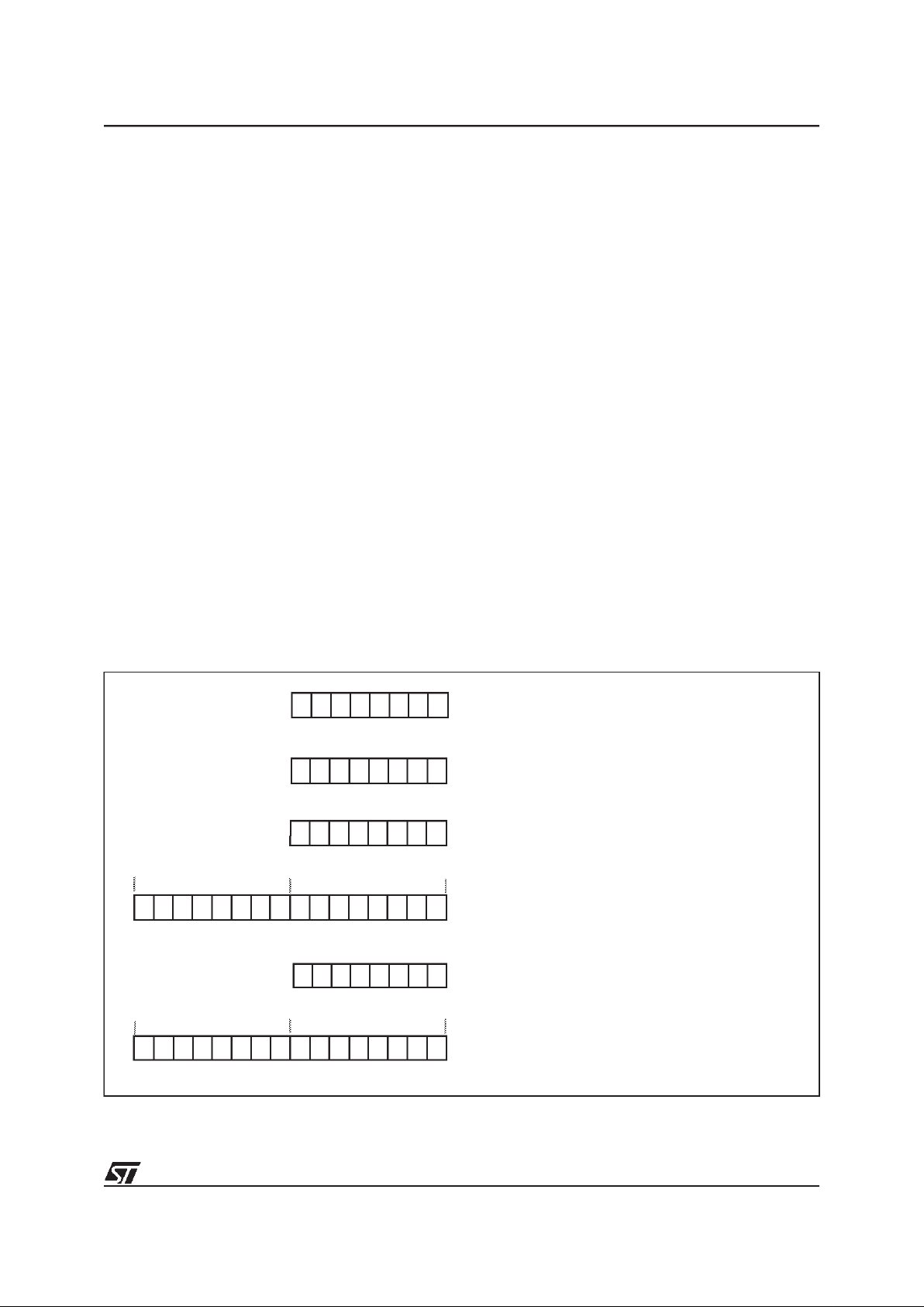
Stack Pointer (SP)
Read/Write
Reset Value: 01 7Fh
The Stack Pointer is a 16-bit register which is always pointingto the next free location in the stack.
It isthen decremented after datahas been pushed
onto the stack and incremented before data is
popped from the stack (see Figure 11).
Since the stack is 64 bytes deep, the 10 most significant bits are forced by hardware. Following an
MCU Reset, or after a Reset Stack Pointer instruction (RSP), the Stack Pointer contains its reset value (the SP5 to SP0 bits are set) which is the stack
higher address.
The least significant byte of the Stack Pointer
(called S) can be directly accessed by a LD instruction.
Note: When the lower limit is exceeded, the Stack
Pointer wraps around tothe stackupper limit, without indicating the stack overflow. The previously
stored information is then overwritten and therefore lost.The stackalso wrapsin caseof anunderflow.
The stack is used to save the return address during a subroutine call and the CPU context during
an interrupt.Theuser may also directly manipulate
the stack by means of the PUSH and POP instructions. In the case ofan interrupt, the PCLis stored
at the first location pointed to by the SP. Then the
other registers are stored in the next locations as
shown in Figure 11.
– Whenan interrupt isreceived, the SP is decre-
mented and the context is pushed on the stack.
– Onreturn from interrupt, the SP is incremented
and thecontext is popped from the stack.
A subroutine call occupies twolocations and aninterrupt five locations in the stack area.
Figure 11. Stack Manipulation Example
15 8
00000001
70
0 1 SP5 SP4 SP3 SP2 SP1 SP0
PCH
PCL
SP
PCH
PCL
SP
PCL
PCH
X
A
CC
PCH
PCL
SP
PCL
PCH
X
A
CC
PCH
PCL
SP
PCL
PCH
X
A
CC
PCH
PCL
SP
SP
Y
CALL
Subroutine
Interrupt
Event
PUSH Y POP Y IRET
RET
or RSP
@ 017Fh
@ 0140h
Stack Lower Address = 0140h
Stack Higher Address =
017Fh
15
Page 16

16/84
ST72101/ST72212/ST72213
3 CLOCKS, RESET, INTERRUPTS & POWER SAVING MODES
3.1 CLOCK SYSTEM
3.1.1 General Description
The MCU accepts either a Crystal or Ceramicresonator, or an external clock signal to drive the internal oscillator. The internal clock (f
CPU
) is de-
rived fromthe external oscillator frequency (f
OSC).
The external Oscillator clock is first divided by 2,
and division factor of 32 can be applied if Slow
Mode is selected by settingthe SMS bit in the Miscellaneous Register. This reduces the frequency
of the f
CPU
; the clock signal is also routed to the
on-chip peripherals.
The internal oscillator is designed to operate with
an AT-cut parallel resonant quartz crystal resonator in the frequency range specified for f
osc
.The
circuit shown in Figure 13 is recommended when
using a crystal, and Table 6 lists the recommended capacitance and feedback resistance values.
The crystal and associated componentsshould be
mounted as close as possible to the input pins in
order to minimize output distortion and start-up
stabilisation time.
Use of an external CMOS oscillator is recommended when crystals outside the specified frequency ranges are to be used.
Table 6. Recommended Values for 16 MHz
Crystal Resonator (C0<7pF)
C0: parasitic shunt capacitance of the quartz crys-
tal.
R
SMAX
: equivalent serialresistor of the crystal (up-
er limit, see crystal specification).
C
OSCOUT,COSCIN
: maximum total capacitance on
OSCIN and OSCOUT, including the external capacitance plus the parasitic capacitance of the
board and the device.
Figure 12. External Clock Source Connections
Figure 13. Crystal/CeramicResonator
Figure 14. Clock Prescaler Block Diagram
R
SMAX
40 Ω 60 Ω 150 Ω
C
OSCIN
56pF 47pF 22pF
C
OSCOUT
56pF 47pF 22pF
OSCIN OSCOUT
EXTERNAL
CLOCK
NC
OSCIN OSCOUT
C
OSCIN
C
OSCOUT
OSCIN
OSCOUT
C
OSCIN
C
OSCOUT
%2 % 16
f
CPU
to CPU and
Peripherals
16
Page 17

17/84
ST72101/ST72212/ST72213
3.2 RESET
3.2.1 Introduction
There are three sources of Reset:
– RESET pin (externalsource)
– Power-On Reset (Internal source)
– WATCHDOG (Internal Source)
The Reset Service Routine vectoris located at ad-
dress FFFEh-FFFFh.
3.2.2 External Reset
The RESET pin is both an input and an open-drain
output with integrated pull-up resistor. When one
of the internal Reset sources is active, the Reset
pin is driven low , for a duration of t
RESET,
to reset
the whole application.
3.2.3 Reset Operation
The duration of the Reset state is a minimum of
4096 internal CPU Clock cycles. During the Reset
state, all I/Os take their reset value.
A Reset signal originating from an externalsource
must have a duration of at least t
PULSE
in order to
be recognised. This detection is asynchronous
and therefore the MCU can enter Reset state even
in Halt mode.
At the end of the Reset cycle, the MCU may be
held in the Reset state by an External Reset signal. The RESET pin may thus be used to ensure
VDDhas risen to a point where theMCU can operate correctly before the user program is run. Fol-
lowing a Reset event, or after exiting Halt mode, a
4096 CPU Clock cycle delay period is initiated in
order to allow the oscillator to stabilise and to ensure that recovery hastaken place from the Reset
state.
In the high state, the RESET pin is connected internally to a pull-up resistor (RON). This resistor
can be pulled low by external circuitry to reset the
device.
The RESET pin is an asynchronous signal which
plays a majorrole in EMS performance. In a noisy
environment, it is recommended to use the external connections shown in Figure8.
3.2.4 Power-on Reset
This circuit detects the ramping up of VDD, and
generates a pulse that is used to reset the application (at approximately VDD= 2V).
Power-On Reset is designed exclusively to cope
with power-up conditions, and should not be used
in order to attempt to detect a drop in the power
supply voltage.
Caution:
to re-initialize the Power-On Reset, the
power supply must fall below approximately 0.8V
(Vtn), prior to rising above 2V. If this condition is
not respected, on subsequent power-upthe Reset
pulse may not be generated. An external Reset
pulse may be required to correctly reactivate the
circuit.
Figure 15. Reset Block Diagram
INTERNAL
RESET
WATCHDOG RESET
OSCILLATOR
SIGNAL
COUNTER
RESET
TO ST7
RESET
POWER-ON RESET
V
DD
R
ON
17
Page 18

18/84
ST72101/ST72212/ST72213
3.3 INTERRUPTS
The ST7 coremaybe interruptedby one of two different methods: maskable hardware interrupts as
listed in the Interrupt Mapping Table and a nonmaskable software interrupt (TRAP). The Interrupt
processing flowchartis shown in Figure16.
The maskable interrupts mustbe enabled clearing
the I bitin order to be serviced. However, disabled
interrupts may be latched and processed when
they are enabled (see external interrupts subsection).
When an interrupt has to be serviced:
– Normal processing is suspended at the end of
the current instruction execution.
– The PC, X, A and CC registersare saved onto
the stack.
– The I bit of the CC register is set to prevent addi-
tional interrupts.
– ThePC is thenloaded with theinterrupt vector of
the interrupt to service and the first instructionof
the interrupt serviceroutine is fetched(refer to
the Interrupt Mapping Table for vector addresses).
The interrupt service routine should finish with the
IRET instruction which causes the contents of the
saved registersto be recovered from thestack.
Note: As a consequence of the IRET instruction,
the I bit will be cleared and the main program will
resume.
Priority management
By default, a servicing interrupt can not be interrupted because the I bit is set by hardware entering in interrupt routine.
In the case several interrupts are simultaneously
pending, an hardware priority defines which one
will be serviced first (seethe Interrupt Mapping Table).
Non Maskable Software Interrupts
This interrupt is entered when the TRAP instruction is executed regardless of the state of theI bit.
It will be serviced according to the flowchart on
Figure 16.
Interrupts and Low power mode
All interrupts allowthe processorto leave the Wait
low power mode. Only external and specific mentioned interrupts allow the processor to leave the
Halt low power mode(referto the “Exit from HALT“
column in the Interrupt Mapping Table).
External Interrupts
External interrupt vectorscan be loaded in the PC
register if the corresponding external interrupt occurred and if the I bit is cleared. These interrupts
allow the processor to leave the Halt low power
mode.
The external interrupt polarity is selected through
the miscellaneous register or interrupt register (if
available).
External interrupt triggered on edge will be latched
and the interrupt request automatically cleared
upon entering the interrupt service routine.
If several input pins, connected to the same interrupt vector, are configured as interrupts, their signals are logically ANDed before entering theedge/
level detection block.
Warning: The type of sensitivity defined in the
Miscellaneous or Interrupt register (if available)
applies to the EI source. In case of an ANDed
source (as described on the I/O ports section), a
low level on an I/O pin configured as input with interrupt, masks the interrupt request even in case
of rising-edge sensitivity.
Peripheral Interrupts
Different peripheral interrupt flags in the status
register are able to cause an interrupt when they
are active if both:
– TheI bit of the CC register is cleared.
– Thecorresponding enablebit is set in thecontrol
register.
If any of these two conditions is false, theinterrupt
is latched and thus remains pending.
Clearing an interrupt request is done by:
– writing “0” to the corresponding bit in the status
register or
– anaccess to the status register while the flag is
set followed bya read or write of anassociated
register.
Note: the clearing sequence resets the internal
latch. A pending interrupt (i.e. waiting for being enabled) will therefore be lost ifthe clear sequence is
executed.
18
Page 19

19/84
ST72101/ST72212/ST72213
INTERRUPTS (Cont’d)
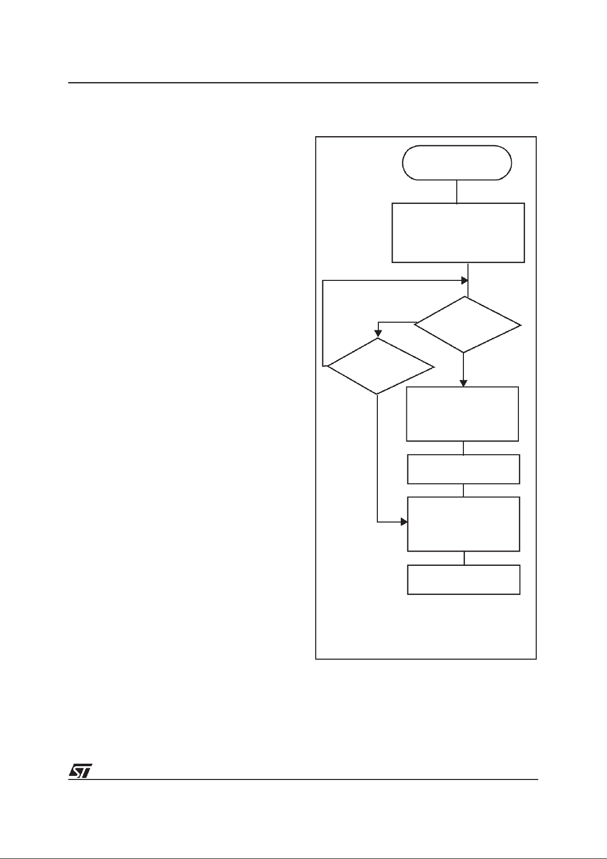
Figure 16. Interrupt Processing Flowchart
BIT I SET
Y
N
IRET
Y
N
FROM RESET
LOAD PC FROM INTERRUPT VECTOR
STACK PC, X, A, CC
SET I BIT
FETCH NEXT INSTRUCTION
EXECUTE INSTRUCTION
THIS CLEARS I BIT BY DEFAULT
RESTORE PC, X, A,CC FROM STACK
BIT I SET
Y
N
19
Page 20
20/84
ST72101/ST72212/ST72213
Table 7. Interrupt Mapping
Note 1: Timer B is available on ST72212 only.
Source
Block
Description
Register
Label
Flag
Exit
from
HALT
Vector
Address
Priority
Order
RESET Reset N/A N/A yes FFFEh-FFFFh
TRAP Software N/A N/A no FFFCh-FFFDh
EI0 External Interrupt PA0:PA7 N/A N/A yes FFFAh-FFFBh
EI1 External Interrupt PB0:PB7, PC0:PC5 N/A N/A yes FFF8h-FFF9h
Not Used FFF6h-FFF7h
SPI
Transfer Complete
SPISR
SPIF
no FFF4h-FFF5h
Mode Fault MODF
TIMER A
Input Capture 1
TASR
ICF1_A
no FFF2h-FFF3h
Output Compare 1 OCF1_A
Input Capture 2 ICF2_A
Output Compare 2 OCF2_A
Timer Overflow TOF_A
Not Used FFF0h-FFF1h
TIMER B
1)
Input Capture 1
TBSR
ICF1_B
no FFEEh-FFEFh
Output Compare 1 OCF1_B
Input Capture 2 ICF2_B
Output Compare 2 OCF2_B
Timer Overflow TOF_B
Not Used
FFECh-FFEDh
FFEAh-FFEBh
FFE8h-FFE9h
FFE6h-FFE7h
FFE4h-FFE5h
FFE2h-FFE3h
FFE0h-FFE1h
Highest
Priority
Priority
Lowest
20
Page 21
21/84
ST72101/ST72212/ST72213
3.4 POWER SAVING MODES
3.4.1 Introduction
There are threePower Saving modes. SlowMode
is selected by setting the relevant bits in the Miscellaneous register. Wait and Halt modes may be
entered usingthe WFI and HALT instructions.
3.4.2 Slow Mode
In Slow mode, the oscillator frequency can be divided by a value defined in the Miscellaneous
Register. The CPU and peripherals are clocked at
this lower frequency. Slow mode isused to reduce
power consumption, andenables the user to adapt
clock frequencyto available supply voltage.
3.4.3 Wait Mode
Wait mode places the MCU in a low power consumption mode by stoppingthe CPU. Allperipherals remain active. During Wait mode, the I bit (CC
Register) is cleared, so as to enable all interrupts.
All otherregisters and memory remain unchanged.
The MCU will remain in Wait mode until an Interrupt or Reset occurs, whereupon the Program
Counter branches to the starting address of the Interrupt orReset Service Routine.
The MCU will remain in Wait mode until a Reset or
an Interrupt occurs, causing it to wake up.
Refer to Figure 17 below.
Figure 17. WAIT Flow Chart
WFI INSTRUCTION
RESET
INTERRUPT
Y
N
N
Y
CPU CLOCK
OSCILLATOR
PERIPH. CLOCK
I-BIT
ON
ON
CLEARED
OFF
Note: Before servicing an interrupt, the CC register is
pushed on the stack. The I-Bit is set during the interrupt routine and cleared when the CC register is
popped.
4096 CPU CLOCK
FETCH RESET VECTOR
OR SERVICE INTERRUPT
CYCLES DELAY
CPU CLOCK
OSCILLATOR
PERIPH. CLOCK
I-BIT
ON
ON
SET
ON
CPU CLOCK
OSCILLATOR
PERIPH. CLOCK
I-BIT
ON
ON
SET
ON
21
Page 22
22/84
ST72101/ST72212/ST72213
POWER SAVINGMODES (Cont’d)
3.4.4 Halt Mode
The Halt mode is the MCU lowest power consumption mode. The Halt mode is entered byexecuting theHALT instruction. The internal oscillator
is then turnedoff, causing allinternal processing to
be stopped, including the operation of the on-chip
peripherals. The Halt mode cannot be used when
the watchdog isenabled, ifthe HALT instruction is
executed while the watchdog system is enabled,a
watchdog reset is generatedthus resetting the entire MCU.
When entering Halt mode, the Ibit in the CC Register is clearedso as toenable ExternalInterrupts.
If an interrupt occurs, the CPU becomes active.
The MCU canexit theHalt mode upon reception of
an interrupt or a reset. Refer to the Interrupt Mapping Table. The oscillator is then turned on and a
stabilization time is provided beforereleasing CPU
operation. Thestabilization timeis 4096 CPU clock
cycles.
After the start up delay, the CPU continuesoperation byservicingthe interrupt whichwakes it up or
by fetching the reset vector if a reset wakes it up.
Figure 18. HALT Flow Chart
N
N
EXTERNAL
INTERRUPT
1)
RESET
HALT INSTRUCTION
4096 CPU CLOCK
FETCH RESET VECTOR
OR SERVICE INTERRUPT
CYCLES DELAY
CPU CLOCK
OSCILLATOR
PERIPH. CLOCK
2)
I-BIT
ON
OFF
SET
ON
CPU CLOCK
OSCILLATOR
PERIPH. CLOCK
I-BIT
OFF
OFF
CLEARED
OFF
Y
Y
WDG
ENABLED?
N
Y
RESET
WATCHDOG
1) or some specific interrupts
Note: Before servicing an interrupt, the CC register is
pushed on the stack. The I-Bit is set during the interrupt routine and cleared when the CC register is
popped.
CPU CLOCK
OSCILLATOR
PERIPH. CLOCK
I-BIT
ON
ON
SET
ON
2) if reset PERIPH. CLOCK = ON ;if interrupt
PERIPH. CLOCK = OFF
22
Page 23

23/84
ST72101/ST72212/ST72213
3.5 MISCELLANEOUS REGISTER
The Miscellaneous register allows to select the
SLOW operatingmode, the polarity of external interrupt requestsand to output the internal clock.
Register Address:0020h — Read/Write
Reset Value: 0000 0000 (00h)
Bit 7:6 = PEI[3:2]
External Interrupt EI1 Polarity
Option
.
These bits are set and cleared by software. They
determine which event on EI1 causes the external interrupt according to Table 8.
Table 8. EI1 External Interrupt Polarity Options
Note: Any modification of one of these twobits re-
sets the interrupt request related to this interrupt
vector.
Bit 5 = MCO
Main Clock Out
This bit isset andcleared by software. When set, it
enables the output of the Internal Clock on the
PC2 I/Oport.
0 -PC2 is a general purpose I/O port.
1 -MCO alternate function (f
CPU
is output on PC2
pin).
Bit 4:3 = PEI[1:0]
External Interrupt EI0 Polarity
Option
.
These bits are set and cleared by software. They
determine which event on EI0 causes the external interrupt according to Table 9.
Table 9. EI0 External Interrupt Polarity Options
Note: Any modification of oneof these two bits re-
sets the interrupt request related to this interrupt
vector.
Bit 1:2 = Unused, always read at 0.
Warning:
Software must write 1 to these bits for
compatibility with future products.
Bit 0 = SMS
Slow Mode Select
This bit is set andcleared by software.
0- Normal mode - f
CPU
= Oscillator frequency / 2
(Reset state)
1- Slow mode - f
CPU
= Oscillatorfrequency /32
70
PEI3 PEI2 MCO PEI1 PEI0 - - SMS
MODE PEI3 PEI2
Falling edge and low level
(Reset state)
00
Falling edge only 1 0
Rising edge only 0 1
Rising and falling edge 1 1
MODE PEI1 PEI0
Falling edge and low level
(Reset state)
00
Falling edge only 1 0
Rising edge only 0 1
Rising and falling edge 1 1
23
Page 24

24/84
ST72101/ST72212/ST72213
4 ON-CHIP PERIPHERALS
4.1 I/O PORTS
4.1.1 Introduction
The I/O ports offer different functional modes:
– transferof data through digital inputsand outputs
and forspecific pins:
– analog signal input (ADC)
– alternate signal input/output for the on-chip pe-
ripherals.
– external interrupt generation
An I/O port is composed of up to 8 pins. Each pin
can be programmedindependently as digital input
(with or without interrupt generation) or digital output.
4.1.2 Functional Description
Each portis associated to 2 main registers:
– Data Register (DR)
– Data Direction Register (DDR)
and someof them to an optional register:
– Option Register (OR)
Each I/Opin may beprogrammed using thecorre-
sponding register bits inDDR and ORregisters: bit
X corresponding to pin Xof the port.The same correspondence is used for the DR register.
The following description takes into account the
OR register, for specific ports whichdo not provide
this register refer to the I/O Port Implementation
Section 4.1.3. The generic I/O block diagram is
shown onFigure 20.
4.1.2.1 Input Modes
The input configuration isselected by clearing the
corresponding DDRregister bit.
In this case, reading the DR register returns the
digital value applied to the external I/O pin.
Different input modes can beselected by software
through theOR register.
Notes:
1. All the inputs are triggered by a Schmitt trigger.
2. When switching from input mode to output
mode, the DR register should be written first to
output the correct value as soon as the port is configured as an output.
Interrupt function
When an I/O is configured in Input with Interrupt,
an event on this I/O can generate an external Interrupt request to the CPU. Theinterrupt polarity is
given independently according to the description
mentioned in the Miscellaneous register or in the
interrupt register (where available).
Each pin can independently generate an Interrupt
request.
Each external interrupt vector is linked to a dedicated group of I/O port pins (see Interrupts section). If several input pins are configured as inputs
to the same interrupt vector, their signals are logically ANDed before entering the edge/level detection block. For this reason if one of the interrupt
pins is tied low, it masks the other ones.
4.1.2.2 Output Mode
The pin is configured in output mode bysetting the
corresponding DDR registerbit.
In this mode, writing “0” or “1” to the DR register
applies this digital value to the I/O pin through the
latch. Then reading the DR register returns the
previously stored value.
Note: In this mode, the interrupt function is disabled.
4.1.2.3 Digital Alternate Function
When an on-chipperipheral is configured to use a
pin, the alternate function is automatically selected. This alternate function takes priority over
standard I/O programming. When the signal is
coming from an on-chip peripheral, the I/O pin is
automatically configuredin output mode (push-pull
or open drain according to theperipheral).
When the signal is going to an on-chip peripheral,
the I/O pin has to be configured ininput mode. In
this case, the pin’s state is also digitally readable
by addressing the DR register.
Notes:
1. Input pull-up configuration can cause an unexpected value atthe input of the alternate peripheral input.
2. When the on-chip peripheral uses apin asinput
and output, this pin must be configured as an input
(DDR = 0).
Warning
: The alternate function must not be acti-
vated as long as the pin isconfigured as inputwith
interrupt, in order to avoid generating spurious interrupts.
24
Page 25

25/84
ST72101/ST72212/ST72213
I/O PORTS (Cont’d)
4.1.2.4 Analog Alternate Function
When the pin isused asan ADC input theI/O must
be configured as input, floating. The analog multiplexer (controlled by the ADC registers) switches
the analog voltage present on the selected pin to
the common analog rail which is connected to the
ADC input.
It isrecommended not to change the voltage level
or loading on any port pin while conversion is in
progress. Furthermore it is recommended not to
have clocking pins located close to a selected analog pin.
Warning
: The analog input voltage level must be
within the limits stated in the Absolute Maximum
Ratings.
4.1.3 I/O Port Implementation
The hardware implementation oneach I/O port depends on the settingsin theDDR andOR registers
and specific feature ofthe I/O portsuch as ADCInput (see Figure 20) or true open drain. Switching
these I/O ports from one state to another should
be done in a sequence that prevents unwanted
side effects. Recommended safetransitions areillustrated in Figure 19. Other transitions are potentially risky and should be avoided, since they are
likely to present unwanted side-effects such as
spurious interrupt generation.
Figure 19. Recommended I/O State Transition Diagram
with interrupt
INPUT
OUTPUT
no interrupt
INPUT
push-pullopen-drain
OUTPUT
25
Page 26
26/84
ST72101/ST72212/ST72213
I/O PORTS (Cont’d)
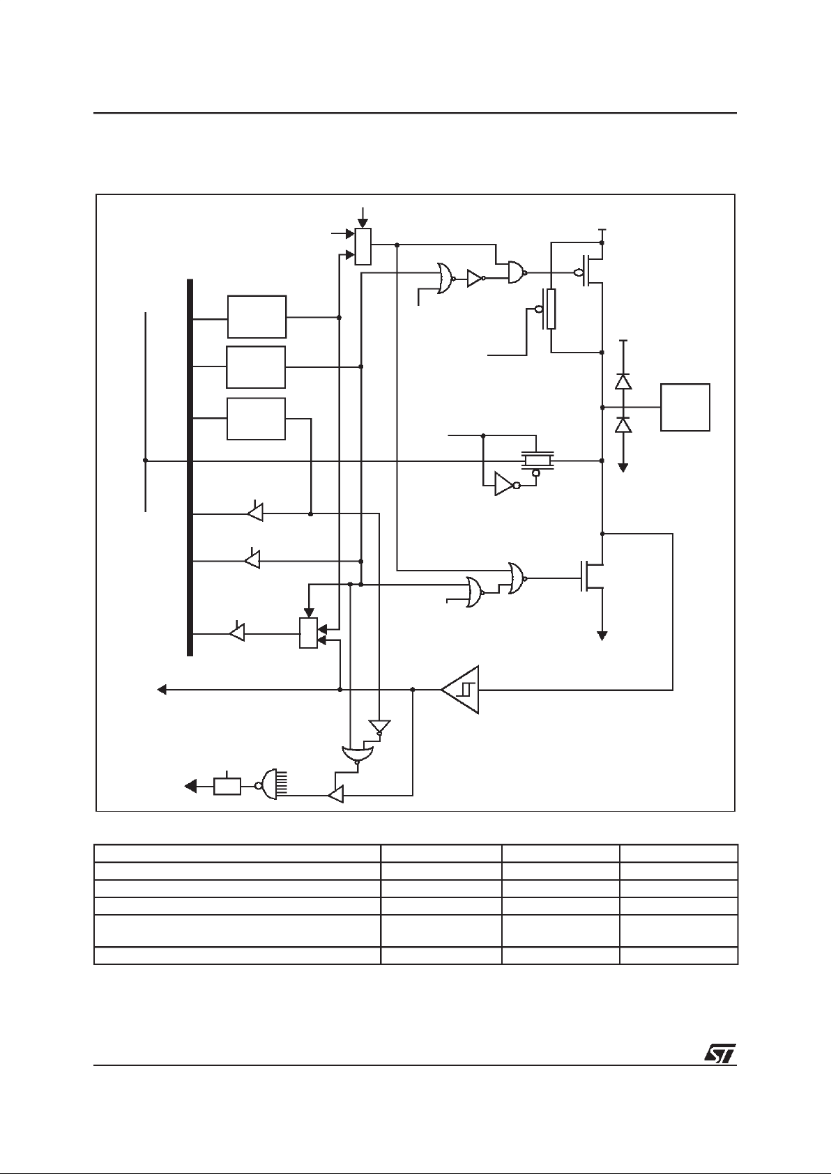
Figure 20. I/O BlockDiagram
Table 10. Port Mode Configuration
Legend:
0 - present, not activated
1 - present and activated
Notes:
– No OR Register on some ports (see register map).
– ADC Switch on ports with analog alternate functions.
DR
DDR
LATCH
LATCH
DATA BUS
DR SEL
DDR SEL
V
DD
PAD
ANALOG
SWITCH
ANALOG ENABLE
(ADC)
M
U
X
ALTERNATE
ALTERNATE
ALTERNATE ENABLE
COMMON ANALOG RAIL
ALTERNATE
M
U
X
ALTERNATE INPUT
PULL-UP
OUTPUT
P-BUFFER
(S
EE TABLE BELOW)
N-BUFFER
1
0
1
0
OR
LATCH
ORSEL
FROM
OTHER
BITS
EXTERNAL
PULL-UP
CONDITION
ENABLE
ENABLE
GND
(S
EE TABLE BELOW)
(S
EE NOTE BELOW)
CMOS
SCHMITT TRIGGER
SOURCE (EIx)
INTERRUPT
POLARITY
SEL
GND
V
DD
DIODE
(SEE TABLEBELOW)
Configuration Mode Pull-up P-buffer V
DD
Diode
Floating 0 0 1
Pull-up 1 0 1
Push-pull 0 1 1
True Open Drain not present not present
not present in OTP
and EPROM devices
Open Drain (logic level) 0 0 1
26
Page 27

27/84
ST72101/ST72212/ST72213
Table 11. Port Configuration
*Reset State
Port Pin Name
Input (DDR = 0) Output (DDR = 1)
OR = 0 OR =1 OR = 0 OR = 1
Port A PA0:PA7 Floating* Floating with Interrupt
True Open Drain,
High Sink Capability
Reserved
Port B PB0:PB7 Floating* Pull-up with Interrupt Open Drain (Logic level) Push-pull
Port C PC0:PC5 Floating* Pull-up with Interrupt Open Drain (Logic level) Push-pull
27
Page 28

28/84
ST72101/ST72212/ST72213
I/O PORTS (Cont’d)
4.1.4 Register Description
4.1.4.1 Data registers
Port A Data Register (PADR)
Port B Data Register (PBDR)
Port C Data Register (PCDR)
Read/Write
Reset Value: 0000 0000 (00h)
Bit 7:0 = D7-D0
Data Register 8 bits.
The DR register has a specific behaviour according to the selected input/output configuration. Writing the DR register is always taken in account
even if the pin is configured as an input. Reading
the DR register returns either theDR register latch
content (pin configuredas output) or the digital value applied to the I/O pin (pin configured as input).
4.1.4.2 Data direction registers
Port A Data Direction Register (PADDR)
Port B Data Direction Register (PBDDR)
Port C Data Direction Register (PCDDR)
Read/Write
Reset Value: 0000 0000 (00h) (input mode)
Bit 7:0 = DD7-DD0
Data Direction Register 8 bits.
The DDR register gives the input/output direction
configuration of the pins. Each bit is set and
cleared by software.
0: Input mode
1: Output mode
4.1.4.3 Option registers
Port A OptionRegister (PAOR)
Port B OptionRegister (PBOR)
Port C Option Register (PCOR)
Read/Write
Reset Value: 0000 0000 (00h) (nointerrupt)
Bit 7:0 = O7-O0
Option Register8 bits.
For specific I/O pins, thisregister is not implemented. In this case the DDR register is enough to select the I/O pin configuration.
The OR register allow to distinguish: in input mode
if the interrupt capability or the floating configuration is selected, in output mode if the push-pull or
open drain configuration is selected.
Each bit is set and clearedby software.
Input mode:
0: floating input
1: input interrupt with or without pull-up
Output mode (only for PB0:PB7, PC0:PC5):
0: output open drain (with P-Bufferinactivated)
1: output push-pull
Output mode (only for PA0:PA7):
0: output open drain
1: reserved
70
D7 D6 D5 D4 D3 D2 D1 D0
70
DD7 DD6 DD5 DD4 DD3 DD2 DD1 DD0
70
O7 O6 O5 O4 O3 O2 O1 O0
28
Page 29

29/84
ST72101/ST72212/ST72213
I/O PORTS (Cont’d)
Table 12. I/O Port RegisterMap and Reset Values
Address
(Hex.)
Register
Label
76543210
0000h
PCDR
Reset Value
D7
0
D6
0
D5
0
D4
0
D37
0
D2
0
D1
0
D0
0
0001h
PCDDR
Reset Value
DD7
0
DD6
0
DD5
0
DD4
0
DD3
0
DD2
0
DD1
0
DD0
0
0002h
PCOR
Reset Value
O7
0
O6
0
O5
0
O4
0
O3
0
O2
0
O1
0
O0
0
0004h
PBDR
Reset Value
D7
0
D6
0
D5
0
D4
0
D37
0
D2
0
D1
0
D0
0
0005h
PBDDR
Reset Value
DD7
0
DD6
0
DD5
0
DD4
0
DD3
0
DD2
0
DD1
0
DD0
0
0006h
PBOR
Reset Value
O7
0
O6
0
O5
0
O4
0
O3
0
O2
0
O1
0
O0
0
0008h
PADR
Reset Value
D7
0
D6
0
D5
0
D4
0
D37
0
D2
0
D1
0
D0
0
0009h
PADDR
Reset Value
DD7
0
DD6
0
DD5
0
DD4
0
DD3
0
DD2
0
DD1
0
DD0
0
000Ah
PAOR
Reset Value
O7
0
O6
0
O5
0
O4
0
O3
0
O2
0
O1
0
O0
0
29
Page 30

30/84
ST72101/ST72212/ST72213
4.2 WATCHDOG TIMER (WDG)
4.2.1 Introduction
The Watchdog timer is used to detect the occurrence of a software fault, usually generated by external interference or by unforeseen logical conditions, which causes the application program to
abandon its normal sequence. The Watchdog circuit generates an MCU reset on expiry of a programmed time period, unless theprogram refreshes the counter’s contents before the T6 bit becomes cleared.
4.2.2 Main Features
■ Programmable timer (64 increments of 12288
CPU cycles)
■ Programmablereset
■ Reset (if watchdog activated) after a HALT
instruction or whenthe T6 bit reaches zero
Figure 21. Watchdog Block Diagram
RESET
WDGA
7-BIT DOWNCOUNTER
f
CPU
T6 T0
CLOCK DIVIDER
WATCHDOG CONTROL REGISTER (CR)
÷12288
T1
T2
T3
T4
T5
30
Page 31

31/84
ST72101/ST72212/ST72213
WATCHDOG TIMER (Cont’d)
4.2.3 Functional Description
The counter value stored in the CR register (bits
T6:T0), is decremented every 12,288 machine cycles, and the length of the timeout period can be
programmed by the user in 64increments.
If the watchdog is activated (the WDGA bit is set)
and when the 7-bit timer (bits T6:T0) rolls over
from 40h to 3Fh (T6 becomes cleared), it initiates
a reset cycle pulling low the reset pin for typically
500ns.
The application program must write in theCR register at regular intervals during normal operation to
prevent an MCU reset. The value to be stored in
the CR register must be between FFh and C0h
(see Table 13):
– The WDGA bit is set (watchdog enabled)
– The T6 bit is set to prevent generating an imme-
diate reset
– TheT5:T0 bits containthenumber ofincrements
which represents the time delay before the
watchdog produces areset.
Table 13. Watchdog Timing (f
CPU
= 8MHz)
Notes: Following a reset, the watchdog is disa-
bled. Onceactivated it cannot be disabled, except
by areset.
The T6 bit can be used to generate a software reset (the WDGA bitis set and the T6 bit is cleared).
If the watchdog is activated, the HALT instruction
will generate a Reset.
4.2.4 Low Power Modes
4.2.5 Interrupts
None.
4.2.6 Register Description
CONTROL REGISTER (CR)
Read/Write
Reset Value: 0111 1111 (7Fh)
Bit 7 = WDGA
Activation bit
.
This bit is set by software and only cleared by
hardware after a reset. When WDGA = 1, the
watchdog can generatea reset.
0: Watchdog disabled
1: Watchdog enabled
Bit 6:0 = T[6:0]
7-bit timer (MSB to LSB).
These bits contain the decremented value. A reset
is produced when it rolls overfrom 40h to 3Fh(T6
becomes cleared).
Table 14. Watchdog Timer Register Map and Reset Values
CR Register
initial value
WDG timeout period
(ms)
Max FFh 98.304
Min C0h 1.536
Mode Description
WAIT No effect on Watchdog.
HALT
Immediate reset generation assoon as
the HALT instruction is executed ifthe
Watchdog is activated(WDGA bit is
set).
70
WDGA T6 T5 T4 T3 T2 T1 T0
Address
(Hex.)
Register
Label
76543210
0024h
WDGCR
Reset Value
WDGA
0
T6
1
T5
1
T4
1
T3
1
T2
1
T1
1
T0
1
31
Page 32

32/84
ST72101/ST72212/ST72213
4.3 16-BIT TIMER
4.3.1 Introduction
The timer consists of a 16-bit free-running counter
driven by a programmable prescaler.
It may be used for a variety of purposes, including
pulse length measurement of up to two input signals (
input capture
) orgeneration of upto two out-
put waveforms (
output compare
and
PWM
).
Pulse lengths and waveform periods can be modulated from a few microseconds to several milliseconds using the timer prescaler and the CPU
clock prescaler.
4.3.2 Main Features
■ Programmableprescaler:f
CPU
dividedby2,4or8.
■ Overflow statusflag and maskable interrupt
■ External clock input (must be at least 4 times
slower thantheCPUclockspeed)withthe choice
of activeedge
■ Output compare functions with
– 2 dedicated 16-bitregisters
– 2 dedicated programmablesignals
– 2 dedicated statusflags
– 1 dedicated maskableinterrupt
■ Input capturefunctions with
– 2 dedicated 16-bitregisters
– 2 dedicated active edge selection signals
– 2 dedicated statusflags
– 1 dedicated maskableinterrupt
■ Pulse widthmodulation mode (PWM)
■ One pulse mode
■ 5 alternatefunctionson I/Oports (ICAP1,ICAP2,
OCMP1, OCMP2, EXTCLK)*
The Block Diagram is shown in Figure 22.
*Note: Some external pins are not available on all
devices. Refer to the devicepin outdescription.
When reading an input signal which is not availa-
ble on an external pin, the value will always be ‘1’.
4.3.3 Functional Description
4.3.3.1 Counter
The principal block of the Programmable Timer is
a 16-bit free running increasing counter and itsassociated 16-bit registers:
Counter Registers
– Counter High Register (CHR) isthe most sig-
nificant byte (MSB).
– Counter Low Register (CLR) is the least sig-
nificant byte (LSB).
Alternate Counter Registers
– AlternateCounter HighRegister (ACHR) is the
most significant byte(MSB).
– AlternateCounter Low Register (ACLR) is the
least significant byte (LSB).
These two read-only 16-bit registers contain the
same value but with the differencethat reading the
ACLR register doesnot clear the TOF bit (overflow
flag), (see note at the end of paragraph titled16-bit
read sequence).
Writing in the CLRregister or ACLR register resets
the free running counter to the FFFCh value.
The timer clock depends on the clock control bits
of the CR2 register, as illustratedin Table 15. The
value in the counter register repeats every
131.072, 262.144 or 524.288 internal processorclock cycles depending on the CC1and CC0 bits.
32
Page 33

33/84
ST72101/ST72212/ST72213
16-BIT TIMER (Cont’d)
Figure 22. Timer Block Diagram
MCU-PERIPHERAL INTERFACE
COUNTER
ALTERNATE
REGISTER
OUTPUT
COMPARE
REGISTER
OUTPUT COMPARE
EDGE DETECT
OVERFLOW
DETECT
CIRCUIT
1/2
1/4
1/8
8-bit
buffer
ST7 INTERNAL BUS
LATCH1
OCMP1
ICAP1
EXTCLK
f
CPU
TIMER INTERRUPT
ICF2ICF1 000OCF2OCF1 TOF
PWMOC1E EXEDGIEDG2CC0CC1
OC2E
OPMFOLV2ICIE OLVL1IEDG1OLVL2FOLV1OCIE TOIE
ICAP2
LATCH2
OCMP2
8
8
8 low
16
8 high
16 16
16
16
CR1
CR2
SR
6
16
888
888
high
low
high
high
high
low
low
low
EXEDG
TIMER INTERNAL BUS
CIRCUIT1
EDGE DETECT
CIRCUIT2
CIRCUIT
1
OUTPUT
COMPARE
REGISTER
2
INPUT
CAPTURE
REGISTER
1
INPUT
CAPTURE
REGISTER
2
CC1 CC0
16 BIT
FREE RUNNING
COUNTER
33
Page 34

34/84
ST72101/ST72212/ST72213
16-BIT TIMER (Cont’d)
16-bit read sequence: (from either the Counter
Register orthe Alternate Counter Register).
The user must read the MSB first, then the LSB
value isbuffered automatically.
This buffered value remains unchanged until the
16-bit read sequence is completed, even if the
user readsthe MSB several times.
After a complete reading sequence, if only the
CLR register or ACLR register are read, they return the LSB of the count value at the time of the
read.
Whatever the timer mode used (input capture, output compare, one pulse mode or PWM mode) an
overflow occurs when the counter rolls over from
FFFFh to0000h then:
– The TOF bitof the SRregister is set.
– A timer interrupt is generated if:
– TOIE bit of the CR1 registeris set and
– I bit ofthe CC register is cleared.
If one of these conditions is false, the interrupt remains pending to be issued as soon as they are
both true.
Clearing the overflow interrupt request is done in
two steps:
1.Reading theSR registerwhile the TOF bit isset.
2.An access (read or write) to the CLR register.
Notes: The TOF bit is not cleared by accesses to
ACLR register. This feature allows simultaneous
use of the overflow function and reads of the free
running counter at random times (for example, to
measure elapsed time) without the risk ofclearing
the TOF biterroneously.
The timer is not affected byWAIT mode.
In HALT mode,the counter stops countinguntil the
mode is exited. Counting then resumes from the
previous count(MCU awakenedby an interrupt) or
from the reset count (MCU awakened by aReset).
4.3.3.2 External Clock
The external clock (where available) is selected if
CC0=1 and CC1=1 in CR2 register.
The status of the EXEDG bit determines the type
of level transition on the external clock pin EXTCLK that willtrigger the free running counter.
The counter is synchronised with the falling edge
of the internal CPU clock.
At least four falling edges of the CPU clock must
occur between two consecutive active edges of
the external clock; thus the external clock frequency must be less than a quarter of the CPU clock
frequency.
LSB is buffered
Read MSB
At t0
Read LSB
Returns the buffered
LSB value at t0
At t0 +∆t
Other
instructions
Beginning of the sequence
Sequence completed
34
Page 35

35/84
ST72101/ST72212/ST72213
16-BIT TIMER (Cont’d)
Figure 23. Counter Timing Diagram, internal clock dividedby 2
Figure 24. Counter Timing Diagram, internal clock dividedby 4
Figure 25. Counter Timing Diagram, internal clock dividedby 8
CPU CLOCK
FFFD FFFE FFFF 0000 0001 0002 0003
INTERNAL RESET
TIMER CLOCK
COUNTER REGISTER
OVERFLOW FLAG TOF
FFFC FFFD 0000 0001
CPU CLOCK
INTERNAL RESET
TIMERCLOCK
COUNTER REGISTER
OVERFLOW FLAG TOF
CPU CLOCK
INTERNAL RESET
TIMER CLOCK
COUNTER REGISTER
OVERFLOW FLAG TOF
FFFC FFFD
0000
35
Page 36

36/84
ST72101/ST72212/ST72213
16-BIT TIMER (Cont’d)
4.3.3.3 Input Capture
In this section, the index,i, may be 1 or 2.
The two input capture 16-bit registers (IC1R and
IC2R) are used to latch the value of the free running counter after a transition detected by the
ICAPipin (see figure 5).
ICiregister is a read-only register.
The active transition is software programmable
through theIEDGibitof theControl Register(CRi).
Timing resolution is one count of the free running
counter: (f
CPU
/(CC1.CC0)).
Procedure:
To use the input capturefunction select thefollowing in the CR2 register:
– Select the timer clock (CC1-CC0) (see Table
15).
– Select the edge of the active transition on the
ICAP2 pin with the IEDG2 bit (the ICAP2 pin
must be configured as floating input).
And selectthe following in theCR1 register:
– Set the ICIE bit to generate an interruptafter an
input capture coming from both the ICAP1 pin or
the ICAP2 pin
– Select the edge of the active transition on the
ICAP1 pin with theIEDG1 bit(the ICAP1pinmust
be configured as floating input).
When an input capture occurs:
– ICFibit is set.
– The ICiR register contains the value of the free
running counter on the active transition on the
ICAPipin (seeFigure 27).
– Atimer interrupt is generatedif the ICIEbit is set
and theI bit is cleared in the CC register.Otherwise, the interrupt remains pending until both
conditions become true.
Clearing the Input Capture interrupt request is
done in two steps:
1.Reading the SRregister while the ICFibitis set.
2.An access (read or write) to the ICiLR register.
Notes:
1.After reading the ICiHR register, transfer of
input capture data is inhibited until the ICiLR
register is also read.
2.The ICiR register always contains the free running counter value which corresponds to the
most recentinput capture.
3.The 2 input capture functions can be used
together even if the timer also uses the output
compare mode.
4.In One pulse Mode and PWM mode only the
input capture 2 can be used.
5.The alternate inputs (ICAP1 & ICAP2) are
always directly connected to the timer. So any
transitions on these pins activate the input capture process.
6.Moreover if one of the ICAPipin is configured
as an input and the second one as an output,
an interrupt can be generated if the user toggle
the output pin and if the ICIE bit isset.
7.The TOF bit can be used with interrupt in order
to measure event that go beyond the timer
range (FFFFh).
MS Byte LS Byte
ICiR IC
i
HR ICiLR
36
Page 37
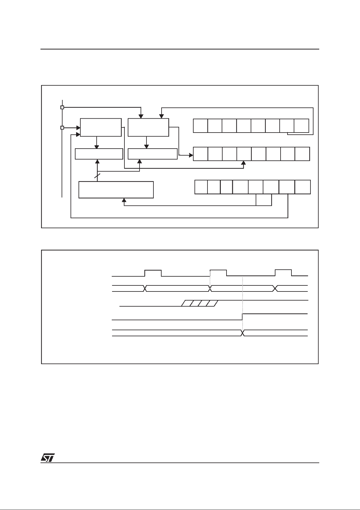
37/84
ST72101/ST72212/ST72213
16-BIT TIMER (Cont’d)
Figure 26. Input Capture Block Diagram
Figure 27. Input Capture Timing Diagram
ICIE
CC0
CC1
16-BIT FREE RUNNING
COUNTER
IEDG1
(Control Register 1) CR1
(Control Register 2) CR2
ICF2ICF1 000
(Status Register) SR
IEDG2
ICAP1
ICAP2
EDGE DETECT
CIRCUIT2
16-BIT
IC1R RegisterIC2R Register
EDGE DETECT
CIRCUIT1
pin
pin
FF01 FF02 FF03
FF03
TIMER CLOCK
COUNTER REGISTER
ICAPi PIN
ICAPi FLAG
ICAPi REGISTER
Note: A
ctive edge is rising edge.
37
Page 38

38/84
ST72101/ST72212/ST72213
16-BIT TIMER (Cont’d)
4.3.3.4 Output Compare
In this section, the index,i, may be 1 or 2.
This function can be used to control an output
waveform or indicating when a period of time has
elapsed.
When a match is found between the Output Compare register and the free running counter, the output compare function:
– Assigns pins with a programmable value if the
OCIE bit is set
– Sets a flag in the status register
– Generates an interrupt if enabled
Two 16-bit registers Output Compare Register 1
(OC1R) and Output Compare Register 2 (OC2R)
contain the value to be compared to the free running counter each timer clock cycle.
These registers are readable and writable and are
not affected by the timer hardware. A reset event
changes the OCiR valueto 8000h.
Timing resolution is one count of the free running
counter: (f
CPU/(CC1.CC0)
).
Procedure:
To use the outputcompare function, select thefollowing in the CR2 register:
– Set the OCiE bit if an output is needed then the
OCMPipin is dedicated to the output compare
i
function.
– Select the timer clock (CC1-CC0) (see Table
15).
And selectthe following in theCR1 register:
– Select theOLVLibitto applied to theOCMPipins
after the matchoccurs.
– Set the OCIE bit to generate an interrupt if it is
needed.
When a match is found:
– OCFibit is set.
– The OCMPipin takes OLVLibit value (OCMP
i
pin latch is forced low during reset andstays low
until valid compares change it to a high level).
– A timer interrupt is generated if the OCIE bit is
set in the CR2 register and the I bit iscleared in
the CC register (CC).
The OCiR register valuerequired for a specifictim-
ing application can be calculated using thefollowing formula:
Where:
∆t = Desired output compare period (in sec-
onds)
f
CPU
= Internal clock frequency
PRESC
= Timer prescaler factor (2, 4 or 8 de-
pending on CC1-CC0 bits, see Table
15)
Clearing the output compare interrupt request is
done by:
1.Reading the SR register while the OCFibit is
set.
2.An access (read or write) to the OCiLR register.
The following procedure is recommended to prevent the OCFibit from being set between the time
it is read and the write to the OCiR register:
– Writeto the OCiHR register (further compares
are inhibited).
– Readthe SR register (firststep of theclearance
of the OCFibit, which may be already set).
– Writeto the OCiLR register (enablesthe output
compare functionand clears the OCFibit).
Notes:
1.After a processor write cycle to the OCiHR register, the output compare function is inhibited
until theOCiLR register is also written.
2.If the OCiE bit is not set, the OCMPipin is a
general I/O port and the OLVLibit will not
appear when a match is found but an interrupt
could be generated if the OCIE bit is set.
3.When the clock is divided by 2, OCFiand
OCMPiare set while the counter value equals
the OCiR register value (see Figure 29, on
page 39). This behaviour is the same in OPM
or PWM mode.
When the clock is divided by 4, 8 or in external
clock mode, OCFiand OCMPiare set while the
counter value equals the OCiR register value
plus 1(see Figure 30, on page39).
4.The output compare functions can be usedboth
for generating external events on the OCMP
i
pins even if the input capture mode is also
used.
5.The value in the 16-bit OCiR register and the
OLVibit should be changed after each successful comparisonin orderto control an output
waveform orestablish a new elapsed timeout.
MS Byte LS Byte
OC
i
ROC
i
HR OCiLR
∆OC
i
R=
∆t*f
CPU
PRESC
38
Page 39

39/84
ST72101/ST72212/ST72213
16-BIT TIMER (Cont’d)
Figure 28. Output Compare BlockDiagram
Figure 29. Output Compare Timing Diagram, Internal Clock Divided by 2
Figure 30. Output Compare Timing Diagram, Internal Clock Divided by 4
OUTPUT COMPARE
16-bit
CIRCUIT
OC1R Register
16 BIT FREE RUNNING
COUNTER
OC1E CC0CC1
OC2E
OLVL1OLVL2OCIE
(Control Register 1) CR1
(Control Register 2) CR2
000OCF2OCF1
(Status Register) SR
16-bit
16-bit
OCMP1
OCMP2
Latch
1
Latch
2
OC2R Register
Pin
Pin
INTERNAL CPU CLOCK
TIMER CLOCK
COUNTER
OUTPUT COMPARE REGISTER
OUTPUT COMPARE FLAG (OCFi)
OCMPi PIN (OLVLi=1)
2ED3
2ED0 2ED1 2ED2
2ED3
2ED42ECF
INTERNAL CPU CLOCK
TIMER CLOCK
COUNTER
OUTPUT COMPARE REGISTER
COMPARE REGISTER LATCH
OCFi AND OCMPi PIN (OLVLi=1)
2ED3
2ED0 2ED1 2ED2
2ED3
2ED42ECF
39
Page 40
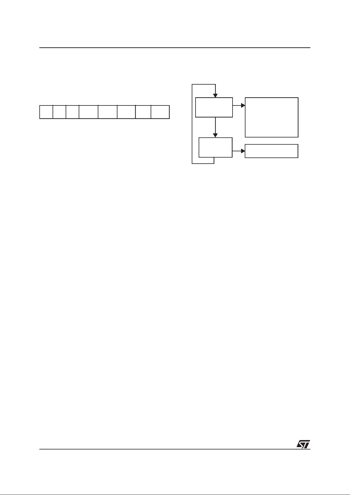
40/84
ST72101/ST72212/ST72213
16-BIT TIMER (Cont’d)
4.3.3.5 Forced Compare
In this sectionimay represent 1 or 2.
The following bits of the CR1 register are used:
When the FOLVibit is set by software, the OLVL
i
bit iscopied to the OCMPipin. The OLVibithas to
be toggled in order to toggle the OCMPipin when
it is enabled (OCiE bit=1). The OCFibitis then not
set by hardware, and thus no interrupt request is
generated.
FOLVLibitshaveno effectin both one pulse mode
and PWMmode.
4.3.3.6 One Pulse Mode
One Pulse mode enables the generation of a
pulse when an externalevent occurs.This mode is
selected viathe OPM bit inthe CR2 register.
The one pulse mode uses the Input Capture1
function and the Output Compare1 function.
Procedure:
To useone pulse mode:
1. Load the OC1R register with the value corresponding to the length of the pulse (see theformula inSection 4.3.3.7).
2. Select the following in the CR1 register:
– Using the OLVL1 bit, select the levelto be ap-
plied to the OCMP1 pin after the pulse.
– Using the OLVL2 bit, select the levelto be ap-
plied to the OCMP1 pin during the pulse.
– Select the edge of the active transition on the
ICAP1 pin with the IEDG1 bit (the ICAP1 pin
must be configured as floating input).
3. Select the following in the CR2 register:
– Set the OC1E bit, the OCMP1 pin is then ded-
icated to the Output Compare 1 function.
– Set the OPM bit.
– Select the timer clock CC1-CC0 (see Table
15).
Then, on a valid event on the ICAP1 pin, the counter is initialized to FFFCh and OLVL2 bit is loaded
on the OCMP1pin, the ICF1 bit is set and thevalue FFFDh is loaded in the IC1R register.
When the value of the counteris equal to the value
of the contents of the OC1R register, the OLVL1
bit is output on the OCMP1pin, (See Figure 31).
Notes:
1.The OCF1 bit cannot be set by hardware in one
pulse mode but the OCF2 bit can generate an
Output Compareinterrupt.
2.The ICF1 bit is set when an active edge occurs
and can generate an interrupt if the ICIE bit is
set.
3.When the Pulse Width Modulation (PWM) and
One Pulse Mode (OPM) bits are both set, the
PWM modeis the only active one.
4.If OLVL1=OLVL2 a continuous signal will be
seen onthe OCMP1 pin.
5.The ICAP1 pin cannot be usedto perform input
capture. TheICAP2 pin can be used to perform
input capture(ICF2 canbe set andIC2R can be
loaded) but the user must take care that the
counter is reset each time a valid edge occurs
on the ICAP1 pin and ICF1 can also generates
interrupt if ICIE is set.
6.When the one pulse mode is used OC1R is
dedicated to this mode. Nevertheless OC2R
and OCF2 can be used to indicate a period of
time has been elapsed but cannot generate an
output waveform because the level OLVL2 is
dedicated to the one pulse mode.
FOLV2 FOLV1 OLVL2 OLVL1
event occurs
Counter
= OC1R
OCMP1 = OLVL1
When
When
on ICAP1
One pulsemode cycle
OCMP1 = OLVL2
Counter is reset
to FFFCh
ICF1 bit is set
40
Page 41
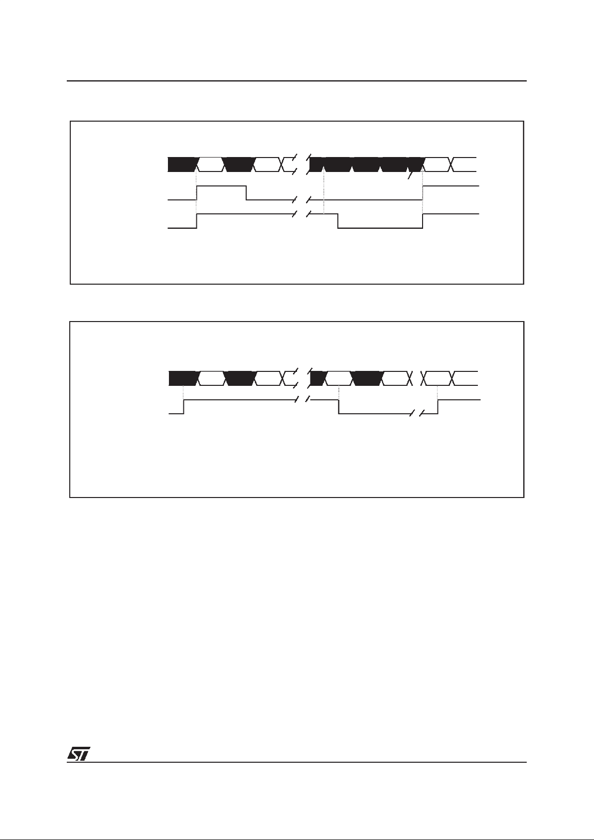
41/84
ST72101/ST72212/ST72213
Figure 31. One Pulse Mode Timing Example
Figure 32. Pulse Width Modulation Mode Timing Example
COUNTER
....
FFFC FFFD FFFE 2ED0 2ED1 2ED2
2ED3
FFFC FFFD
OLVL2
OLVL2OLVL1
ICAP1
OCMP1
compare1
Note: IEDG1=1, OC1R=2ED0h, OLVL1=0, OLVL2=1
COUNTER
34E2 FFFC FFFD FFFE 2ED0 2ED1 2ED2 34E2 FFFC
OLVL2
OLVL2OLVL1
OCMP1
compare2 compare1 compare2
Note: OC1R=2ED0h, OC2R=34E2, OLVL1=0, OLVL2= 1
41
Page 42
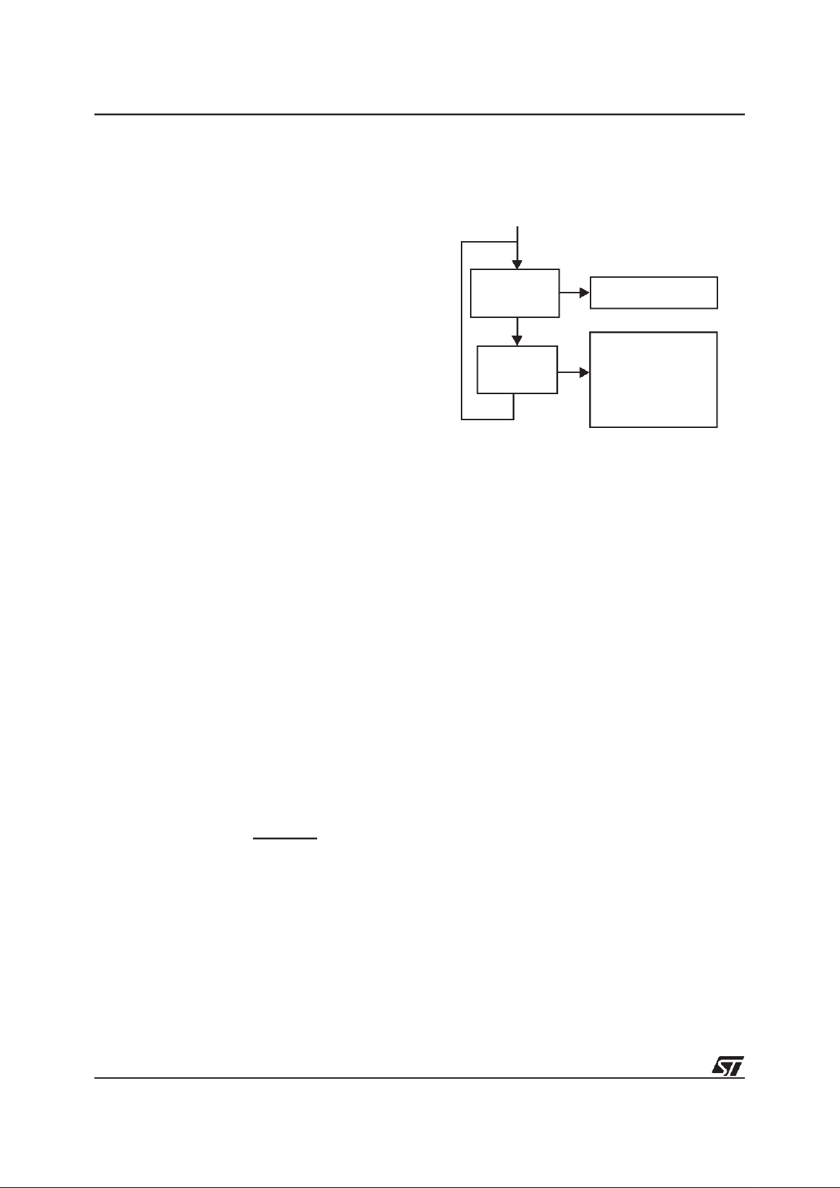
42/84
ST72101/ST72212/ST72213
16-BIT TIMER (Cont’d)
4.3.3.7 Pulse Width Modulation Mode
Pulse Width Modulation(PWM)mode enables the
generation of a signal with a frequency and pulse
length determined by the value of the OC1R and
OC2R registers.
The pulse width modulation mode uses the complete Output Compare 1 function plus the OC2R
register, and so these functionality can not be
used whenthe PWM mode is activated.
Procedure
To usepulse width modulation mode:
1. Load the OC2R register with the value corresponding to the period of the signal.
2. Load the OC1R register with the value corresponding to the length of the pulse if (OLVL1=0
and OLVL2=1).
3. Select the following in the CR1 register:
– Using the OLVL1 bit, select the levelto be ap-
plied to the OCMP1 pin after a successful
comparison with OC1R register.
– Using the OLVL2 bit, select the levelto be ap-
plied to the OCMP1 pin after a successful
comparison with OC2R register.
4. Select the following in the CR2 register:
– Set OC1E bit: the OCMP1 pinis thendedicat-
ed to the output compare 1 function.
– Set the PWM bit.
– Select the timer clock (CC1-CC0) (see Table
15).
If OLVL1=1 and OLVL2=0 the length of the positive pulse is the difference betweenthe OC2R and
OC1R registers.
If OLVL1=OLVL2 a continuous signal will be seen
on the OCMP1 pin.
The OCiR register valuerequired for a specifictiming application can be calculated using thefollowing formula:
Where:
t = Desired output compare period (in sec-
onds)
f
CPU
= Internal clock frequency
PRESC
= Timer prescaler factor (2, 4 or 8 de-
pending on CC1-CC0 bits, see Table
15)
The Output Compare 2 event causes the counter
to be initializedto FFFCh (SeeFigure 32).
Notes:
1.After a write instruction to the OCiHR register,
the output compare function is inhibited until the
OCiLR register is also written.
Therefore the Input Capture 1 function is inhibited but the Input Capture2 is available.
2.The OCF1 and OCF2 bits cannot be set by
hardware in PWM mode therefore the Output
Compare interruptis inhibited.
3.The ICF1 bit is set by hardware when the counter reaches the OC2R value and can produce a
timer interrupt if theICIE bit is setand the I bit is
cleared.
4.In PWM mode the ICAP1 pin can not be used
to perform input capture because it is disconnected tothe timer.The ICAP2 pin can beused
to perform input capture (ICF2 can be set and
IC2R can be loaded) but the user must take
care that the counter is reset each period and
ICF1 canalso generates interrupt if ICIE is set.
5.When the Pulse Width Modulation (PWM) and
One Pulse Mode (OPM) bits are both set, the
PWM modeis the only active one.
OCiR Value=
t*f
CPU
PRESC
-5
Counter
OCMP1 = OLVL2
Counter
= OC2R
OCMP1 = OLVL1
When
When
= OC1R
Pulse Width Modulation cycle
Counter is reset
to FFFCh
ICF1 bitis set
42
Page 43

43/84
ST72101/ST72212/ST72213
16-BIT TIMER (Cont’d)
4.3.4 LowPower Modes
4.3.5 Interrupts
Note: The 16-bit Timer interrupt events are con-
nected tothe sameinterrupt vector(see Interrupts
chapter).
These events generate an interrupt if the corresponding Enable Control Bit is set and the I-bit in
the CC register is reset (RIM instruction).
Mode Description
WAIT
No effect on 16-bit Timer.
Timer interrupts cause the device to exit from WAIT mode.
HALT
16-bit Timer registers are frozen.
In HALT mode, the counter stops counting until Halt mode is exited. Counting resumes from the previous
count whenthe MCU is woken up by an interrupt with “exit from HALT mode” capability or fromthe counter
reset value when the MCU is woken up by a RESET.
If an input capture event occurs on the ICAP
i
pin, the input capture detection circuitry is armed. Consequent-
ly, when the MCU is woken up by an interrupt with“exit from HALT mode” capability, the ICF
i
bit is set, and
the counter value present when exiting from HALT mode is captured into the IC
i
R register.
Interrupt Event
Event
Flag
Enable
Control
Bit
Exit
from
Wait
Exit
from
Halt
Input Capture 1 event/Counter reset in PWM mode ICF1
ICIE
Yes No
Input Capture 2 event ICF2 Yes No
Output Compare 1 event (not available in PWM mode) OCF1
OCIE
Yes No
Output Compare 2 event (not available in PWM mode) OCF2 Yes No
Timer Overflow event TOF TOIE Yes No
43
Page 44

44/84
ST72101/ST72212/ST72213
16-BIT TIMER (Cont’d)
4.3.6 Register Description
Each Timer is associated with three control and
status registers, and with six pairsof data registers
(16-bit values) relating to the two input captures,
the two output compares, the counter and the alternate counter.
CONTROL REGISTER 1 (CR1)
Read/Write
Reset Value: 0000 0000 (00h)
Bit 7 = ICIE
Input Capture Interrupt Enable.
0: Interrupt is inhibited.
1: A timer interrupt is generated whenever the
ICF1 or ICF2 bit of the SR register isset.
Bit 6 = OCIE
Output Compare Interrupt Enable.
0: Interrupt is inhibited.
1: A timer interrupt is generated whenever the
OCF1 or OCF2 bit of the SR register is set.
Bit 5 = TOIE
Timer Overflow Interrupt Enable.
0: Interrupt is inhibited.
1: A timer interrupt is enabled whenever the TOF
bit of the SR register is set.
Bit 4 = FOLV2
Forced Output Compare 2.
This bit is set andcleared by software.
0: No effecton the OCMP2 pin.
1:Forces the OLVL2 bit to be copied to the
OCMP2 pin, if the OC2E bit is set and even if
there isno successful comparison.
Bit 3 = FOLV1
Forced Output Compare 1.
This bit is set andcleared by software.
0: No effecton the OCMP1 pin.
1: Forces OLVL1 to becopied to theOCMP1 pin,if
the OC1E bit is set and even if there is no successful comparison.
Bit 2 = OLVL2
Output Level 2.
This bit is copied to the OCMP2 pin whenever a
successful comparison occurs withthe OC2Rregister and OCxE is set in the CR2 register.This value is copied to the OCMP1 pinin One Pulse Mode
and Pulse Width Modulation mode.
Bit 1 = IEDG1
Input Edge1.
This bit determines which type of level transition
on the ICAP1 pin will trigger the capture.
0: A falling edge triggers the capture.
1: A rising edge triggers the capture.
Bit 0 = OLVL1
Output Level 1.
The OLVL1 bit is copied to the OCMP1 pin whenever a successful comparison occurs with the
OC1R register and the OC1E bit is set in the CR2
register.
70
ICIE OCIE TOIE FOLV2 FOLV1 OLVL2 IEDG1 OLVL1
44
Page 45

45/84
ST72101/ST72212/ST72213
16-BIT TIMER (Cont’d)
CONTROL REGISTER 2 (CR2)
Read/Write
Reset Value: 0000 0000 (00h)
Bit 7 = OC1E
Output Compare 1 Pin Enable.
This bit is used only to output the signal from the
timer on the OCMP1 pin (OLV1 in Output Compare mode, both OLV1 and OLV2 in PWM and
one-pulse mode). Whateverthe value of theOC1E
bit, the Output Compare1 function of the timer remains active.
0: OCMP1 pin alternate function disabled (I/O pin
free for general-purpose I/O).
1: OCMP1 pin alternate function enabled.
Bit 6 = OC2E
Output Compare 2 Enable.
This bit is used only to output the signal from the
timer on the OCMP2 pin (OLV2 in Output Compare mode). Whatever the value of the OC2E bit,
the Output Compare 2 function of the timer remains active.
0: OCMP2 pin alternate function disabled (I/O pin
free for general-purpose I/O).
1: OCMP2 pin alternate function enabled.
Bit 5 = OPM
One PulseMode.
0: One Pulse Mode is not active.
1: One PulseMode isactive, theICAP1 pin can be
used totrigger one pulseon the OCMP1 pin; the
active transition is given by the IEDG1 bit. The
length of the generated pulse depends on the
contents of the OC1R register.
Bit 4 = PWM
Pulse WidthModulation.
0: PWM modeis not active.
1: PWM mode is active, the OCMP1 pin outputs a
programmable cyclic signal; the length of the
pulse depends on the value of OC1R register;
the period depends on the valueof OC2R register.
Bit 3, 2 = CC1-CC0
Clock Control.
The value ofthe timer clock depends onthese bits:
Table 15. Clock Control Bits
Bit 1 = IEDG2
Input Edge2.
This bit determines which type of level transition
on the ICAP2 pin will trigger the capture.
0: A falling edge triggers the capture.
1: A rising edge triggers the capture.
Bit 0 = EXEDG
External Clock Edge.
This bit determines which type of level transition
on the external clock pin EXTCLK will trigger the
free running counter.
0: A falling edge triggers the freerunning counter.
1: A rising edge triggers the free running counter.
70
OC1E OC2E OPM PWM CC1 CC0 IEDG2 EXEDG
Timer Clock CC1 CC0
f
CPU
/4 0 0
f
CPU
/2 0 1
f
CPU
/8 1 0
External Clock (where
available)
11
45
Page 46

46/84
ST72101/ST72212/ST72213
16-BIT TIMER (Cont’d)
STATUS REGISTER (SR)
Read Only
Reset Value: 0000 0000 (00h)
The three least significant bits arenot used.
Bit 7 = ICF1
Input Capture Flag 1.
0: No input capture (reset value).
1: An input capture has occurred or the counter
has reached the OC2R value in PWM mode. To
clear thisbit, firstread the SRregister, then read
or write the low byte of the IC1R (IC1LR) register.
Bit 6 = OCF1
Output Compare Flag 1.
0: No match (reset value).
1: The content of the free running counter has
matched the content of the OC1R register. To
clear thisbit, firstread the SRregister, then read
or writethe low byte of the OC1R (OC1LR) register.
Bit 5 = TOF
Timer Overflow.
0: No timer overflow (reset value).
1:The freerunning counter rolled overfrom FFFFh
to 0000h. To clear thisbit, first read the SR register, then read or write the low byte of the CR
(CLR) register.
Note: Reading or writing the ACLR register does
not clear TOF.
Bit 4 = ICF2
Input Capture Flag 2.
0: No input capture (reset value).
1: An input capture has occurred.To clear this bit,
first read the SR register, then read or write the
low byte of the IC2R (IC2LR) register.
Bit 3 = OCF2
Output Compare Flag 2.
0: No match (reset value).
1: The content of the free running counter has
matched the content of the OC2R register. To
clear thisbit, firstread the SRregister, then read
or writethe low byte of the OC2R (OC2LR) register.
Bit 2-0 = Reserved, forced by hardware to 0.
INPUT CAPTURE 1 HIGH REGISTER (IC1HR)
Read Only
Reset Value: Undefined
This is an8-bit read only register thatcontains the
high part of the counter value (transferred by the
input capture 1 event).
INPUT CAPTURE 1 LOW REGISTER (IC1LR)
Read Only
Reset Value: Undefined
This is an8-bit read only register thatcontains the
low part of the counter value (transferred by the input capture 1 event).
OUTPUT COMPARE 1 HIGH REGISTER
(OC1HR)
Read/Write
Reset Value: 1000 0000 (80h)
This is an 8-bit register that contains the high part
of the value to be comparedto the CHR register.
OUTPUT COMPARE 1 LOW REGISTER
(OC1LR)
Read/Write
Reset Value: 0000 0000 (00h)
This isan 8-bitregister that containsthelow part of
the value to be compared to the CLR register.
70
ICF1 OCF1 TOF ICF2 OCF2 0 0 0
70
MSB LSB
70
MSB LSB
70
MSB LSB
70
MSB LSB
46
Page 47

47/84
ST72101/ST72212/ST72213
16-BIT TIMER (Cont’d)
OUTPUT COMPARE 2 HIGH REGISTER
(OC2HR)
Read/Write
Reset Value: 1000 0000 (80h)
This is an 8-bit register that contains the high part
of the value to be comparedto the CHRregister.
OUTPUT COMPARE 2 LOW REGISTER
(OC2LR)
Read/Write
Reset Value: 0000 0000 (00h)
This is an 8-bitregister that contains thelow part of
the value to be compared tothe CLR register.
COUNTER HIGH REGISTER (CHR)
Read Only
Reset Value: 1111 1111 (FFh)
This is an 8-bit register that contains the high part
of the counter value.
COUNTER LOW REGISTER (CLR)
Read Only
Reset Value: 1111 1100 (FCh)
This is an 8-bitregister that contains thelow part of
the counter value. A writeto thisregisterresets the
counter. Anaccess to this registerafter accessing
the SR register clears the TOF bit.
ALTERNATE COUNTER HIGH REGISTER
(ACHR)
Read Only
Reset Value: 1111 1111 (FFh)
This is an 8-bit register that contains the high part
of the counter value.
ALTERNATE COUNTER LOW REGISTER
(ACLR)
Read Only
Reset Value: 1111 1100 (FCh)
This isan 8-bitregister that containsthelow part of
the counter value. Awrite to this register resets the
counter. An access to this register after anaccess
to SR register does not clear the TOF bit in SR
register.
INPUT CAPTURE 2 HIGH REGISTER (IC2HR)
Read Only
Reset Value: Undefined
This is an8-bit read only register thatcontains the
high part of the counter value (transferred by the
Input Capture 2 event).
INPUT CAPTURE 2 LOW REGISTER (IC2LR)
Read Only
Reset Value: Undefined
This is an8-bit read only register thatcontains the
low part of thecounter value(transferred by the Input Capture 2 event).
70
MSB LSB
70
MSB LSB
70
MSB LSB
70
MSB LSB
70
MSB LSB
70
MSB LSB
70
MSB LSB
70
MSB LSB
47
Page 48

48/84
ST72101/ST72212/ST72213
16-BIT TIMER (Cont’d)
Table 16. 16-Bit Timer Register Map and Reset Values
Address
(Hex.)
Register
Name
76543210
TimerA: 32
TimerB: 42
CR1
Reset Value
ICIE
0
OCIE
0
TOIE0FOLV20FOLV10OLVL20IEDG10OLVL1
0
TimerA: 31
TimerB: 41
CR2
Reset Value
OC1E
0
OC2E
0
OPM
0
PWM
0
CC1
0
CC0
0
IEDG20EXEDG
0
TimerA: 33
TimerB: 43SRReset Value
ICF1
0
OCF1
0
TOF
0
ICF2
0
OCF2
0
-
0
-
0
-
0
TimerA: 34
TimerB: 44
IC1HR
Reset Value
MSB
-
------
LSB
TimerA: 35
TimerB: 45
IC1LR
Reset Value
MSB
-
------
LSB
TimerA: 36
TimerB: 46
OC1HR
Reset Value
MSB
1
-
0
-
0
-
0
-
0
-
0
-
0
LSB
0
TimerA: 37
TimerB: 47
OC1LR
Reset Value
MSB
0
-
0
-
0
-
0
-
0
-
0
-
0
LSB
0
TimerA: 3E
TimerB: 4E
OC2HR
Reset Value
MSB
1
-
0
-
0
-
0
-
0
-
0
-
0
LSB
0
TimerA: 3F
TimerB: 4F
OC2LR
Reset Value
MSB
0
-
0
-
0
-
0
-
0
-
0
-
0
LSB
0
TimerA: 38
TimerB: 48
CHR
Reset Value
MSB
1111111
LSB
1
TimerA: 39
TimerB: 49
CLR
Reset Value
MSB
1111110
LSB
0
TimerA: 3A
TimerB: 4A
ACHR
Reset Value
MSB
1111111
LSB
1
TimerA: 3B
TimerB: 4B
ACLR
Reset Value
MSB
1111110
LSB
0
TimerA: 3C
TimerB: 4C
IC2HR
Reset Value
MSB
-
------
LSB
TimerA: 3D
TimerB: 4D
IC2LR
Reset Value
MSB
-
------
LSB
-
48
Page 49

49/84
ST72101/ST72212/ST72213
4.4 SERIAL PERIPHERAL INTERFACE (SPI)
4.4.1 Introduction
The Serial Peripheral Interface (SPI) allows fullduplex, synchronous, serial communication with
external devices. An SPI system may consist of a
master and one or more slaves or a system in
which devices may be either mastersor slaves.
The SPI is normally used for communication between themicrocontroller and external peripherals
or another microcontroller.
Refer to the Pin Descriptionchapter for the devicespecific pin-out.
4.4.2 Main Features
■ Full duplex, three-wire synchronous transfers
■ Master orslave operation
■ Four mastermode frequencies
■ Maximum slave mode frequency = fCPU/2.
■ Four programmablemaster bit rates
■ Programmable clock polarity and phase
■ End of transfer interrupt flag
■ Write collision flag protection
■ Master modefault protection capability.
4.4.3 General description
The SPI is connected to external devices through
4 alternate pins:
– MISO: Master In Slave Out pin
– MOSI: Master Out Slave In pin
– SCK: Serial Clock pin
– SS: Slave select pin
A basic example of interconnections between a
single master and a single slave is illustrated on
Figure 33.
The MOSI pins are connected together as are
MISO pins. In this way data is transferred serially
between master and slave (most significant bit
first).
When the master device transmits data to a slave
device via MOSI pin, the slave device responds by
sending data to the master device via the MISO
pin. This implies full duplex transmission with both
data out and data in synchronized with the same
clock signal (which is provided by the master device via the SCK pin).
Thus, the byte transmitted is replacedby the byte
received and eliminates the need for separate
transmit-empty and receiver-full bits. A status flag
is used to indicate that the I/O operation is complete.
Four possible data/clock timing relationships may
be chosen (see Figure 36) but master and slave
must be programmed with the same timing mode.
Figure 33. Serial Peripheral Interface Master/Slave
8-BIT SHIFT REGISTER
SPI
CLOCK
GENERATOR
8-BIT SHIFT REGISTER
MISO
MOSI
MOSI
MISO
SCK
SCK
SLAVE
MASTER
SS
SS
+5V
MSBit LSBit MSBit LSBit
49
Page 50

50/84
ST72101/ST72212/ST72213
SERIAL PERIPHERAL INTERFACE (Cont’d)
Figure 34. Serial Peripheral Interface Block Diagram
DR
Read Buffer
8-Bit Shift Register
Write
Read
Internal Bus
SPI
SPIE SPE SPR2 MSTR CPHA SPR0SPR1CPOL
SPIF
WCOL
MODF
SERIAL
CLOCK
GENERATOR
MOSI
MISO
SS
SCK
CONTROL
STATE
CR
SR
-
--
--
IT
request
MASTER
CONTROL
50
Page 51

51/84
ST72101/ST72212/ST72213
SERIAL PERIPHERAL INTERFACE (Cont’d)
4.4.4 Functional Description
Figure 33 shows the serial peripheral interface
(SPI) blockdiagram.
This interface contains 3 dedicated registers:
– A Control Register (CR)
– A Status Register (SR)
– A Data Register (DR)
Refer to the CR, SR and DR registers in Section
4.4.7for the bit definitions.
4.4.4.1 Master Configuration
In a master configuration, the serial clock is generated onthe SCK pin.
Procedure
– Select the SPR0 & SPR1 bits todefine these-
rial clock baud rate (see CR register).
– Select the CPOL and CPHA bits todefine one
of the four relationships between the data
transfer and the serial clock (see Figure 36).
– The SS pin must be connected to ahigh level
signal during the complete byte transmit sequence.
– The MSTR and SPE bits must beset (they re-
main set only if the SS pin is connected to a
high level signal).
In this configuration the MOSI pin is a data output
and to the MISO pin is a data input.
Transmit sequence
The transmit sequencebegins when abyte is written the DRregister.
The data byte is parallel loaded into the 8-bit shift
register (from the internal bus)during a writecycle
and then shifted out serially to the MOSI pin most
significant bit first.
When data transfer is complete:
– The SPIF bit is set by hardware
– An interrupt is generatedif the SPIE bit is set
and the I bit in the CCR register is cleared.
During the last clock cycle the SPIF bit is set, a
copy of the data byte received in the shift register
is moved to a buffer. Whenthe DR register isread,
the SPI peripheralreturns this buffered value.
Clearing the SPIF bit isperformed bythe following
software sequence:
1.An access to the SR registerwhile the SPIF bit
is set
2.A write ora read of the DR register.
Note: While the SPIF bit is set, all writes to the DR
51
Page 52

52/84
ST72101/ST72212/ST72213
SERIAL PERIPHERAL INTERFACE (Cont’d)
4.4.4.2 Slave Configuration
In slave configuration, the serial clock is received
on the SCK pin from themaster device.
The value of the SPR0& SPR1 bits is not used for
the data transfer.
Procedure
– For correct data transfer, the slave device
must be in the same timing mode asthe master device (CPOL and CPHA bits).See Figure
36.
– The SS pin must be connected to a low level
signal during the complete byte transmit sequence.
– Clear the MSTRbit and set the SPE bit to as-
sign the pins to alternate function.
In this configuration the MOSI pin is a data input
and theMISO pin is a data output.
Transmit Sequence
The data byte is parallel loaded into the 8-bit shift
register (from the internalbus) during a write cycle
and then shifted out serially to the MISO pin most
significant bit first.
The transmit sequence begins whenthe slave device receivesthe clock signal and the most significant bit of the data on its MOSI pin.
When data transfer is complete:
– The SPIF bit is set by hardware
– An interrupt is generatedif SPIE bit is set and
I bit in CCR register iscleared.
During the last clock cycle the SPIF bit is set, a
copy of the data byte received in the shift register
is moved to a buffer. Whenthe DR register isread,
the SPI peripheralreturns this buffered value.
Clearing the SPIF bit isperformed bythe following
software sequence:
1.An access to the SR registerwhile the SPIF bit
is set.
2.A write ora read of the DR register.
Notes: While the SPIF bit is set, all writes to the
DR register are inhibited until the SR register is
read.
The SPIF bit can be cleared during a second
transmission; however, it must be cleared before
the second SPIF bit in order to prevent an overrun
condition (see Section 4.4.4.6).
Depending on the CPHA bit, the SS pin has to be
set to write to the DR register between each data
byte transfer to avoid awrite collision(see Section
4.4.4.4).
52
Page 53

53/84
ST72101/ST72212/ST72213
SERIAL PERIPHERAL INTERFACE (Cont’d)
4.4.4.3 Data Transfer Format
During an SPI transfer, data is simultaneously
transmitted (shifted out serially) and received
(shifted in serially). Theserial clock isused tosynchronize the data transfer during a sequence of
eight clockpulses.
The SS pin allows individual selection of a slave
device; theother slave devices that are notselected do not interfere with the SPI transfer.
Clock Phase and Clock Polarity
Four possible timing relationships may be chosen
by software,using the CPOL and CPHA bits.
The CPOL (clock polarity) bit controls the steady
state value of the clock when no data is being
transferred. This bit affects both master andslave
modes.
The combination between the CPOL and CPHA
(clock phase) bits selects the data capture clock
edge.
Figure 36, shows an SPI transfer with the four
combinations of the CPHAand CPOL bits. Thediagram may be interpreted as a master or slave
timing diagram where the SCK pin, the MISO pin,
the MOSI pin are directly connected between the
master and theslave device.
The SS pin is the slavedevice select input andcan
be driven by the master device.
The master device applies data to its MOSI pinclock edge before the capture clockedge.
CPHA bit is set
The second edge on the SCK pin (falling edge if
the CPOL bit is reset, rising edge if the CPOL bit is
set) is theMSBit capture strobe. Data islatched on
the occurrence of the first clock transition.
No write collision should occur even if the SS pin
stays low during a transfer of several bytes (see
Figure 35).
CPHA bit is reset
The firstedge on theSCKpin (falling edge ifCPOL
bit is set, rising edge if CPOL bit is reset) is the
MSBit capture strobe. Data is latched on the occurrence of the second clock transition.
This pin must be toggled high and low between
each byte transmitted (see Figure 35).
To protect the transmission froma writecollision a
low value on the SS pin of a slave device freezes
the data in its DR register and does not allow it to
be altered. Therefore the SS pin must be high to
write a new data byte in the DR without producing
a write collision.
Figure 35. CPHA / SS Timing Diagram
MOSI/MISO
Master
SS
Slave SS
(CPHA=0)
Slave
SS
(CPHA=1)
Byte 1 Byte 2
Byte 3
VR02131A
53
Page 54

54/84
ST72101/ST72212/ST72213
SERIAL PERIPHERAL INTERFACE (Cont’d)
Figure 36. Data Clock Timing Diagram
CPOL = 1
CPOL =0
MSBit Bit 6 Bit 5
Bit 4 Bit3 Bit 2 Bit 1 LSBit
MISO
(from master)
MOSI
(from slave)
SS
(to slave)
CAPTURE STROBE
CPHA =1
CPOL = 1
CPOL = 0
MSBit Bit 6 Bit 5
Bit 4 Bit3 Bit 2 Bit 1 LSBit
MSBit Bit 6 Bit 5 Bit 4 Bit3 Bit 2 Bit 1 LSBit
MISO
(from master)
MOSI
SS
(to slave)
CAPTURE STROBE
CPHA =0
Note: This figureshould not be usedas a replacement forparametric information.
Refer to the Electrical Characteristics chapter.
(from slave)
VR02131B
MSBit Bit 6 Bit 5
Bit 4 Bit3 Bit 2 Bit 1 LSBit
54
Page 55
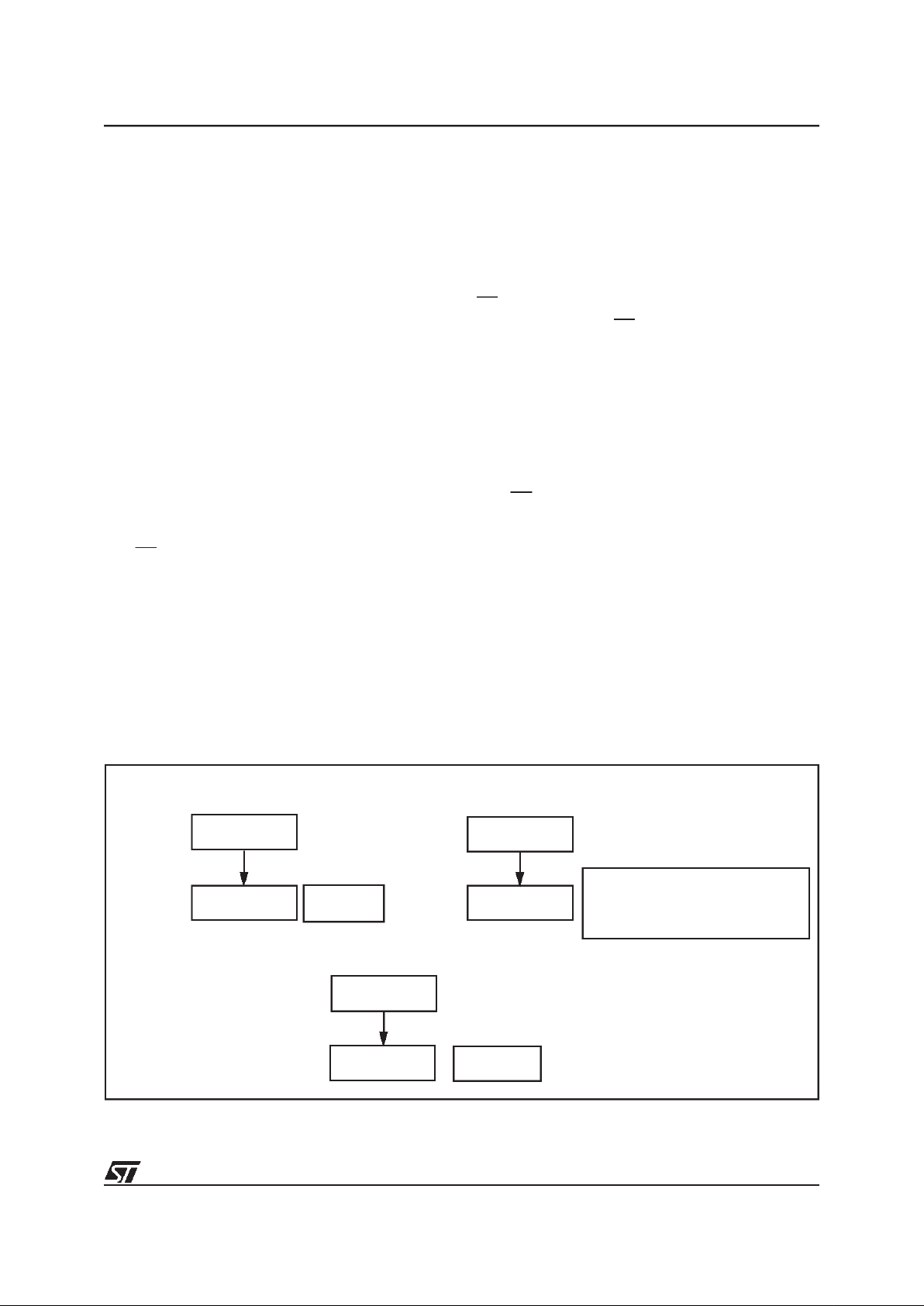
55/84
ST72101/ST72212/ST72213
SERIAL PERIPHERAL INTERFACE (Cont’d)
4.4.4.4 Write Collision Error
A write collision occurs when the software tries to
write to the DR register while a data transfer is taking place with an external device. When this happens, the transfer continues uninterrupted; and
the software write will be unsuccessful.
Write collisions can occurboth inmaster and slave
mode.
Note: a ”read collision” will never occur since the
received data byte is placed in a buffer in which
access is alwayssynchronous withthe MCU operation.
In Slave mode
When the CPHA bit is set:
The slave device will receive a clock (SCK) edge
prior to the latch of the first data transfer. This first
clock edgewill freeze the data in the slave device
DR register and output the MSBit on to the external MISO pin of the slave device.
The SS pin lowstate enables the slave device but
the output of the MSBit onto the MISO pin does
not take place until the first data transfer clock
edge.
When the CPHA bit is reset:
Data is latchedon the occurrence of thefirst clock
transition. The slave device does not have any
way of knowing when that transition will occur;
therefore, the slave device collision occurs when
software attempts to write the DR registerafter its
SS pin has been pulled low.
For this reason, the SS pin mustbe high, between
each data byte transfer, to allow the CPU to write
in the DR register without generating a write collision.
In Master mode
Collision in the master device is definedas a write
of the DR register while the internal serial clock
(SCK) is in the process of transfer.
The SS pin signal must be always high on the
master device.
WCOL bit
The WCOL bit in the SR register is set if a write
collision occurs.
No SPI interrupt is generated when the WCOL bit
is set (the WCOL bit is a status flagonly).
Clearing the WCOLbit is done through a software
sequence (see Figure37).
Figure 37. Clearing the WCOLbit (Write Collision Flag) Software Sequence
Clearing sequence after SPIF = 1(end of a databyte transfer)
1st Step
Read SR
Read DR Write DR
2nd Step
SPIF =0
WCOL=0
SPIF =0
WCOL=0 if no transfer has started
WCOL=1 if a transfer has started
Clearing sequence before SPIF = 1 (during a data byte transfer)
1st Step
2nd Step
WCOL=0
before the 2nd step
Read SR
Read DR
Note: Writing in DR register instead of reading in it do not reset
WCOL bit
Read SR
OR
THEN
THEN
THEN
55
Page 56

56/84
ST72101/ST72212/ST72213
SERIAL PERIPHERAL INTERFACE (Cont’d)
4.4.4.5 Master Mode Fault
Master mode fault occurs when the master device
has its SS pin pulled low, then the MODF bit isset.
Master mode fault affectstheSPI peripheral in the
following ways:
– The MODF bit is set and an SPI interrupt is
generated if theSPIE bit is set.
– The SPE bit is reset. This blocks all output
from the device and disables the SPI peripheral.
– The MSTR bit is reset,thus forcingthe device
into slave mode.
Clearing theMODF bit is done through a software
sequence:
1. A read or write access to the SR register while
the MODF bit is set.
2. A writeto the CR register.
Notes: To avoid any multiple slave conflicts in the
case of a system comprising several MCUs, the
SS pinmust be pulled high during the clearingsequence of the MODF bit. The SPE and MSTRbits
may be restored to their original state during or after this clearing sequence.
Hardware does not allow the user to set the SPE
and MSTR bits while the MODFbit isset exceptin
the MODF bit clearing sequence.
In a slave device the MODF bit can notbe set, but
in a multi masterconfiguration the device can be in
slave mode with this MODF bit set.
The MODF bit indicates that there might have
been a multi-master conflict for system control and
allows a proper exitfrom systemoperation toa reset or default system state using an interrupt routine.
4.4.4.6 Overrun Condition
An overrun condition occurs, when themaster device has sent several data bytes and the slavedevice has not cleared the SPIF bit issuing from the
previous data bytetransmitted.
In this case, the receiver buffer contains the byte
sent after the SPIF bit was last cleared. A read to
the DR register returns this byte. All other bytes
are lost.
This condition isnot detected by the SPIperipheral.
56
Page 57

57/84
ST72101/ST72212/ST72213
SERIAL PERIPHERAL INTERFACE (Cont’d)
4.4.4.7 Single Master and Multimaster Configurations
There are two types of SPI systems:
– Single Master System
– Multimaster System
Single MasterSystem
A typical single master systemmay beconfigured,
using an MCU as the master and four MCUs as
slaves (see Figure 38).
The master device selects the individualslave devices byusing fourpins ofa parallel port to control
the four SS pinsof the slave devices.
The SS pins are pulled high during reset since the
master device ports will be forced to be inputs at
that time,thus disabling the slave devices.
Note: To prevent a bus conflict on the MISO line
the master allows only one slave device during a
transmission.
For more security, the slave device may respond
to the masterwith thereceived data byte. Then the
master willreceivethe previous byte backfrom the
slave device if all MISO and MOSI pins are connected and the slave has not written its DR register.
Other transmission security methods can use
ports for handshake lines or data bytes with command fields.
Multi-master System
A multi-master system may also be configured by
the user. Transfer of master control could be implemented using a handshake method through the
I/O ports or by an exchange of code messages
through the serial peripheral interface system.
The multi-master system is principally handled by
the MSTR bit in the CRregister and the MODF bit
in the SR register.
Figure 38. Single Master Configuration
MISO
MOSI
MOSI
MOSI MOSI MOSIMISO MISO MISOMISO
SS
SS
SS
SS
SS
SCK SCK
SCK
SCK
SCK
5V
Ports
Slave
MCU
Slave
MCU
Slave
MCU
Slave
MCU
Master
MCU
57
Page 58

58/84
ST72101/ST72212/ST72213
SERIAL PERIPHERAL INTERFACE (Cont’d)
4.4.5 LowPower Modes
4.4.6 Interrupts
Note: The SPI interrupt events are connected to
the same interrupt vector (see Interrupts chapter).
They generate an interrupt if the corresponding
Enable Control Bitis set and the I-bitin the CCregister is reset (RIM instruction).
Mode Description
WAIT
No effect on SPI.
SPI interrupt events cause the device to exit from WAIT mode.
HALT
SPI registers are frozen.
In HALT mode, the SPI is inactive. SPI operation resumes when the MCU is woken up by an interrupt with
“exit from HALT mode” capability.
Interrupt Event
Event
Flag
Enable
Control
Bit
Exit
from
Wait
Exit
from
Halt
SPI End of Transfer Event SPIF
SPIE
Yes No
Master Mode Fault Event MODF Yes No
58
Page 59
59/84
ST72101/ST72212/ST72213
SERIAL PERIPHERAL INTERFACE (Cont’d)
4.4.7 Register Description
CONTROL REGISTER (CR)
Read/Write
Reset Value: 0000xxxx (0xh)
Bit 7 = SPIE
Serial peripheral interrupt enable.
This bit is set and cleared by software.
0: Interrupt is inhibited
1: An SPI interruptis generated whenever SPIF=1
or MODF=1in the SR register
Bit 6 = SPE
Serial peripheral output enable.
This bit is set and cleared by software. It is also
cleared by hardware when, inmaster mode, SS=0
(see Section 4.4.4.5 Master Mode Fault).
0: I/O port connected to pins
1: SPI alternate functions connected to pins
The SPE bit is clearedby reset,so the SPI peripheral isnot initially connected to the external pins.
Bit 5 = SPR2
Divider Enable
.
this bit is set and cleared by software and it is
cleared by reset.It is usedwith theSPR[1:0] bits to
set the baud rate. Refer to Table 17.
0: Divider by 2 enabled
1: Divider by 2 disabled
Bit 4 = MSTR
Master.
This bit is set and cleared by software. It is also
cleared by hardware when, inmaster mode, SS=0
(see Section 4.4.4.5 Master Mode Fault).
0: Slave mode is selected
1: Master mode is selected, the function of the
SCK pin changesfrom an input to an output and
the functions ofthe MISO and MOSI pinsare reversed.
Bit 3 = CPOL
Clock polarity.
This bit is setand cleared by software. This bit determines the steady state of the serial Clock. The
CPOL bit affects both the master and slave
modes.
0: The steady state is a low value at the SCK pin.
1: The steady state is a high value at the SCK pin.
Bit 2 = CPHA
Clock phase.
This bit is set andcleared by software.
0: The first clock transition isthe firstdata capture
edge.
1: The second clock transition is the first capture
edge.
Bit 1:0 = SPR[1:0]
Serial peripheral rate.
These bits are set and cleared by software.Used
with the SPR2 bit,they select one of six baudrates
to be used as the serial clock when the deviceis a
master.
These 2 bits have no effectin slave mode.
Table 17. Serial Peripheral Baud Rate
70
SPIE SPE SPR2 MSTR CPOL CPHA SPR1 SPR0
Serial Clock SPR2 SPR1 SPR0
f
CPU
/2 1 0 0
f
CPU
/8 0 0 0
f
CPU
/16 0 0 1
f
CPU
/32 1 1 0
f
CPU
/64 0 1 0
f
CPU
/128 0 1 1
59
Page 60

60/84
ST72101/ST72212/ST72213
SERIAL PERIPHERAL INTERFACE (Cont’d)
STATUS REGISTER (SR)
Read Only
Reset Value: 0000 0000 (00h)
Bit 7 = SPIF
Serial Peripheral data transfer flag.
This bit is set by hardware when a transfer has
been completed. An interrupt is generated if
SPIE=1 in the CR register. It is cleared by a software sequence (an access to the SR register followed by a read or write to the DR register).
0: Data transfer is in progressor has beenap-
proved by a clearing sequence.
1: Data transfer between the device and an exter-
nal device has been completed.
Note: While the SPIFbit is set, allwrites to the DR
register are inhibited.
Bit 6 = WCOL
Write Collision status.
This bit is set by hardware when a write to the DR
register is done during a transmit sequence. It is
cleared by a software sequence (see Figure 37).
0: No write collision occurred
1: A write collision has been detected
Bit 5 = Unused.
Bit 4 = MODF
Mode Fault flag.
This bit is set by hardware when the SS pin is
pulled low in master mode (see Section 4.4.4.5
Master Mode Fault). An SPI interrupt can be generated if SPIE=1 in the CR register. This bit is
cleared by a software sequence (An accessto the
SR register while MODF=1 followed by a write to
the CR register).
0: No master mode fault detected
1: A fault in master mode has been detected
Bits 3-0= Unused.
DATA I/O REGISTER (DR)
Read/Write
Reset Value: Undefined
The DR register is used to transmit and receive
data on the serial bus. In the master device only a
write to this register will initiate transmission/reception of anotherbyte.
Notes: During the last clock cycle the SPIF bit is
set, a copy of the received data byte in the shift
register is movedto a buffer. Whenthe user reads
the serial peripheral data I/O register, the buffer is
actually being read.
Warning:
A write to theDR register places data directly into
the shift register fortransmission.
A write to the the DR register returns the value located in the bufferand notthe contentsof the shift
register (See Figure 34 ).
70
SPIF WCOL - MODF - - - -
70
D7 D6 D5 D4 D3 D2 D1 D0
60
Page 61
61/84
ST72101/ST72212/ST72213
SERIAL PERIPHERAL INTERFACE (Cont’d)
Table 18. SPI Register Map and Reset Values
Address
(Hex.)
Register
Name
76543210
21
DR
Reset Value
D7
x
D6
x
D5
x
D4
x
D3
x
D2
x
D1
x
D0
x
22
CR
Reset Value
SPIE
0
SPE
0
SPR20MSTR
0
CPOL
x
CPHA
x
SPR1
x
SPR0
x
23
SR
Reset Value
SPIF
0
WCOL
0
-
0
MODF
0
-
0
-
0
-
0
-
0
61
Page 62

62/84
ST72101/ST72212/ST72213
4.5 8-BIT A/D CONVERTER (ADC)
4.5.1 Introduction
The on-chip Analog to Digital Converter (ADC) peripheral is a 8-bit, successive approximation converter with internal sample and hold circuitry. This
peripheral has up to 8 multiplexed analog input
channels (refer to device pin out description) that
allow the peripheral to convert the analog voltage
levels from up to 8 different sources.
The result of the conversion is stored in a 8-bit
Data Register. The A/D converter is controlled
through a Control/Status Register.
4.5.2 Main Features
■ 8-bit conversion
■ Up to 8 channels with multiplexed input
■ Linear successive approximation
■ Data register (DR) which contains the results
■ Conversioncomplete status flag
■ On/off bit (to reduce consumption)
The block diagram is shown in Figure 39.
Figure 39. ADC block diagram
SAMPLE
ANALOG
MUX
AIN0
AIN1
AIN2
AIN3
AIN4
AIN5
AIN6
AIN7
(Control Status Register) CSR
(Data Register) DR
&
HOLD
f
CPU
ANALOG TO
DIGITAL
CONVERTER
COCO
0CH0CH1CH2-- ADON
AD7
AD4 AD0AD1AD2AD3AD6 AD5
62
Page 63

63/84
ST72101/ST72212/ST72213
8-BIT A/D CONVERTER (ADC) (Cont’d)
4.5.3 Functional Description
The high level reference voltage V
DDA
must be
connected externallyto the VDDpin. The low level
reference voltage V
SSA
must be connected externally to the VSSpin. In some devices (refer to device pin out description) high and low level reference voltages are internally connected to the V
DD
and VSSpins.
Conversion accuracy may therefore be degraded
by voltage drops and noise in the event of heavily
loaded orbadly decoupled power supply lines.
Figure 40. Recommended Ext. Connections
Characteristics:
The conversion is monotonic, meaning the result
never decreases if the analog input does not and
never increases if the analog input does not.
If input voltage is greater than or equal to V
DD
(voltage reference high) then results = FFh (full
scale) withoutoverflow indication.
If input voltage ≤ VSS(voltage reference low) then
the results = 00h.
The conversion time is 64 CPU clock cycles including asampling time of 31.5 CPU clock cycles.
R
AIN
is the maximum recommended impedance
for an analog input signal. If the impedance is too
high, this will result in a loss of accuracy due to
leakage and sampling not being completed in the
alloted time.
The A/D converter is linear and the digital result of
the conversion is given by theformula:
Where Reference Voltage is VDD-VSS.
The accuracy of the conversion is describedin the
Electrical Characteristics Section.
Procedure:
Refer to the CSRand DRregister description section for the bit definitions.
Each analog input pin must be configured as input,
no pull-up, no interrupt. Refer to the «I/O ports»
chapter. Using these pins as analog inputs does
not affect the abilityof the port to beread as a logic
input.
In the CSR register:
– Select the CH2 to CH0 bits to assign the ana-
log channel toconvert. Refer to Table 19.
– Set the ADON bit. Then the A/D converter is
enabled after a stabilization time (typically 30
µs). It then performs a continuous conversion
of the selected channel.
When a conversionis complete
– The COCO bit is set by hardware.
– No interrupt isgenerated.
– The result is in the DR register.
A write to the CSR register aborts the current conversion, resets the COCO bit and starts a new
conversion.
4.5.4 Low Power Modes
Note: The A/D converter may be disabled by re-
setting the ADON bit. This feature allows reduced
power consumption when no conversion is needed.
4.5.5 Interrupts
None
ST7
Px.x/AINx
V
DDA
V
SSA
1K
V
DD
0.1µF
R
AIN
V
AIN
Digital result =
255 x Input Voltage
Reference Voltage
Mode Description
WAIT No effect on A/D Converter
HALT
A/D Converterdisabled.
After wakeup from Halt mode, theA/D
Converter requires a stabilisation time
before accurate conversionscan be
performed.
63
Page 64

64/84
ST72101/ST72212/ST72213
8-BIT A/D CONVERTER (ADC) (Cont’d)
4.5.6 Register Description
CONTROL/STATUS REGISTER (CSR)
Read/Write
Reset Value: 0000 0000 (00h)
Bit 7 = COCO
Conversion Complete
This bit is set by hardware. It is cleared by software readingthe resultin the DRregister or writing
to the CSR register.
0: Conversion is not complete.
1: Conversion can be read from theDR register.
Bit 6 = Reserved. Must always be cleared.
Bit 5 = ADON
A/D converter On
This bit is set and cleared by software.
0: A/D converter is switched off.
1: A/D converter is switched on.
Note: a typically 30µs delay time is necessary for
the ADC tostabilize when the ADON bit is set.
Bit 4 = Reserved. Forced by hardware to 0.
Bit 3 = Reserved. Must always be cleared.
Bits 2-0:CH[2:0]
Channel Selection
These bits are set and cleared by software. They
select the analog input to convert.
Table 19. Channel Selection
*IMPORTANT NOTE:
The number of pins AND
the channel selection vary according to the device.
REFER TO THEDEVICE PINOUT).
DATA REGISTER (DR)
Read Only
Reset Value: 0000 0000 (00h)
Bit 7:0 = AD[7:0]
Analog Converted Value
This register contains the converted analog value
in the range 00h to FFh.
Reading this registerreset the COCOflag.
Table 20. ADC Register Map
70
COCO - ADON 0 - CH2 CH1 CH0
Pin* CH2 CH1 CH0
AIN0 0 0 0
AIN1 0 0 1
AIN2 0 1 0
AIN3 0 1 1
AIN4 1 0 0
AIN5 1 0 1
AIN6 1 1 0
AIN7 1 1 1
70
AD7 AD6 AD5 AD4 AD3 AD2 AD1 AD0
Address
(Hex.)
Register
Name
765 43210
70
Reset Value
DR
AD7
0
AD6
0
AD5
0
AD4
0
AD3
0
AD2
0
AD1
0
AD0
0
71
Reset Value
CSR
COCO
0
-
0
ADON
0
0
0
-
0
CH2
0
CH1
0
CH0
0
64
Page 65

65/84
ST72101/ST72212/ST72213
5 INSTRUCTION SET
5.1 ST7 ADDRESSING MODES
The ST7 Core features 17 different addressing
modes which can be classified in7 main groups:
The ST7 Instruction set is designed to minimize
the number ofbytes requiredper instruction: To do
so, most of the addressing modes may be subdivided in two sub-modes called long andshort:
– Longaddressing mode is more powerful be-
cause itcan use thefull64 Kbyte addressspace,
however it uses more bytes and more CPU cycles.
– Short addressing mode isless powerfulbecause
it can generally only access page zero (0000h 00FFh range),but the instruction size ismore
compact, andfaster. All memory to memory instructions use short addressing modes only
(CLR, CPL,NEG, BSET, BRES, BTJT, BTJF,
INC, DEC, RLC, RRC, SLL, SRL, SRA, SWAP)
The ST7 Assembler optimizes the use of long and
short addressing modes.
Table 21. ST7 Addressing Mode Overview
Note 1. At the time the instruction is executed,the Program Counter (PC) points to the instructionfollowing JRxx.
Addressing Mode Example
Inherent nop
Immediate ld A,#$55
Direct ld A,$55
Indexed ld A,($55,X)
Indirect ld A,([$55],X)
Relative jrne loop
Bit operation bset byte,#5
Mode Syntax
Destination/
Source
Pointer
Address
(Hex.)
Pointer
Size
(Hex.)
Length
(Bytes)
Inherent nop + 0
Immediate ld A,#$55 + 1
Short Direct ld A,$10 00..FF + 1
Long Direct ld A,$1000 0000..FFFF + 2
No Offset Direct Indexed ld A,(X) 00..FF
+ 0 (with X register)
+ 1 (with Y register)
Short Direct Indexed ld A,($10,X) 00..1FE + 1
Long Direct Indexed ld A,($1000,X) 0000..FFFF + 2
Short Indirect ld A,[$10] 00..FF 00..FF byte + 2
Long Indirect ld A,[$10.w] 0000..FFFF 00..FF word + 2
Short Indirect Indexed ld A,([$10],X) 00..1FE 00..FF byte + 2
Long Indirect Indexed ld A,([$10.w],X) 0000..FFFF 00..FF word + 2
Relative Direct jrne loop PC-128/PC+127
1)
+1
Relative Indirect jrne [$10] PC-128/PC+127
1)
00..FF byte + 2
Bit Direct bset $10,#7 00..FF + 1
Bit Indirect bset [$10],#7 00..FF 00..FF byte + 2
Bit Direct Relative btjt $10,#7,skip 00..FF + 2
Bit Indirect Relative btjt [$10],#7,skip 00..FF 00..FF byte + 3
65
Page 66

66/84
ST72101/ST72212/ST72213
ST7 ADDRESSING MODES (Cont’d)
5.1.1 Inherent
All Inherent instructions consist of a single byte.
The opcode fully specifies all the required information for theCPU to process the operation.
5.1.2 Immediate
Immediate instructions have two bytes, the first
byte contains the opcode, the second byte contains the the operand value. .
5.1.3 Direct
In Direct instructions, theoperands are referenced
by their memory address.
The direct addressing mode consists of two submodes:
Direct (short)
The address is a byte, thus requires only one byte
after the opcode, but only allows 00 - FF addressing space.
Direct (long)
The address is a word, thus allowing 64 Kbyte addressing space, but requires 2 bytes after the opcode.
5.1.4 Indexed (No Offset, Short, Long)
In this mode, the operand is referenced by its
memory address,which is defined by the unsigned
addition of an index register (X or Y)with an offset.
The indirect addressing mode consists of three
sub-modes:
Indexed (No Offset)
There is nooffset, (noextra byteafter the opcode),
and allows 00 - FF addressingspace.
Indexed (Short)
The offset is a byte, thus requires only one byteafter the opcode and allows 00 - 1FE addressing
space.
Indexed (long)
The offset is a word, thus allowing 64 Kbyte addressing space and requires 2 bytes after the opcode.
5.1.5 Indirect (Short, Long)
The required data byteto do the operation is found
by itsmemory address, located in memory (pointer).
The pointer address follows the opcode. The indirect addressing mode consists of two sub-modes:
Indirect (short)
The pointer addressis a byte, thepointer size is a
byte, thus allowing 00 - FFaddressing space, and
requires 1 byteafter the opcode.
Indirect (long)
The pointer addressis a byte, thepointer size is a
word, thus allowing 64 Kbyte addressing space,
and requires 1 byte after the opcode.
Inherent Instruction Function
NOP No operation
TRAP S/W Interrupt
WFI
Wait For Interrupt (Low Power
Mode)
HALT
Halt Oscillator (Lowest Power
Mode)
RET Sub-routine Return
IRET Interrupt Sub-routine Return
SIM Set Interrupt Mask
RIM Reset Interrupt Mask
SCF Set Carry Flag
RCF Reset Carry Flag
RSP Reset Stack Pointer
LD Load
CLR Clear
PUSH/POP Push/Pop to/from the stack
INC/DEC Increment/Decrement
TNZ Test Negative or Zero
CPL, NEG 1 or 2 Complement
MUL Byte Multiplication
SLL, SRL, SRA, RLC,
RRC
Shift and Rotate Operations
SWAP Swap Nibbles
Immediate Instruction Function
LD Load
CP Compare
BCP Bit Compare
AND, OR, XOR Logical Operations
ADC, ADD, SUB, SBC Arithmetic Operations
66
Page 67

67/84
ST72101/ST72212/ST72213
ST7 ADDRESSING MODES (Cont’d)
5.1.6 Indirect Indexed (Short, Long)
This is acombination of indirect and short indexed
addressing modes. The operand is referenced by
its memory address, which is defined by the unsigned addition of an index register value (X or Y)
with apointer value located in memory. The pointer address followsthe opcode.
The indirect indexed addressing mode consists of
two sub-modes:
Indirect Indexed(Short)
The pointer address is a byte, the pointer size is a
byte, thus allowing 00 - 1FE addressing space,
and requires1 byte after the opcode.
Indirect Indexed(Long)
The pointer address is a byte, the pointer size is a
word, thus allowing 64 Kbyte addressing space,
and requires1 byte after the opcode.
Table 22. Instructions Supporting Direct,
Indexed, Indirect and Indirect Indexed
Addressing Modes
5.1.7 Relative mode (Direct, Indirect)
This addressing mode is used to modify the PC
register value, by adding an 8-bit signed offset to
it.
The relative addressing mode consists oftwo submodes:
Relative (Direct)
The offset is following the opcode.
Relative (Indirect)
The offset is defined in memory, which address
follows the opcode.
Long and Short
Instructions
Function
LD Load
CP Compare
AND, OR, XOR Logical Operations
ADC, ADD, SUB, SBC
Arithmetic Addition/subtraction operations
BCP Bit Compare
Short Instructions Only Function
CLR Clear
INC, DEC Increment/Decrement
TNZ Test Negative or Zero
CPL, NEG 1 or 2 Complement
BSET, BRES Bit Operations
BTJT, BTJF
Bit Test and Jump Operations
SLL, SRL, SRA, RLC,
RRC
Shift and Rotate Operations
SWAP Swap Nibbles
CALL, JP Call or Jump subroutine
Available Relative Direct/
Indirect Instructions
Function
JRxx Conditional Jump
CALLR Call Relative
67
Page 68

68/84
ST72101/ST72212/ST72213
5.2 INSTRUCTION GROUPS
The ST7 family devices use an Instruction Set
consisting of 63 instructions. The instructions may
be subdivided into 13 main groups as illustrated in
the following table:
Using a pre-byte
The instructions are described with one to four
bytes.
In order to extend the number of available opcodes for an 8-bitCPU (256opcodes), three different prebyte opcodes are defined. These prebytes
modify the meaning of the instruction they precede.
The whole instruction becomes:
PC-2 End of previous instruction
PC-1 Prebyte
PC opcode
PC+1 Additional word (0 to 2) according
to the numberof bytesrequired tocompute the effective address
These prebytes enable instruction in Y as well as
indirect addressing modes to be implemented.
They precede the opcode of the instruction in X or
the instruction using direct addressing mode. The
prebytes are:
PDY 90 Replace an X based instruction
using immediate, direct, indexed, or inherent addressing mode by a Y one.
PIX 92 Replace an instruction using direct, direct bit, or direct relative addressing mode
to an instruction using the corresponding indirect
addressing mode.
It also changesan instruction using Xindexed addressing modeto an instruction using indirect Xindexed addressing mode.
PIY 91 Replace an instruction using X indirect indexed addressing mode by a Y one.
Load and Transfer LD CLR
Stack operation PUSH POP RSP
Increment/Decrement INC DEC
Compare and Tests CP TNZ BCP
Logical operations AND OR XOR CPL NEG
Bit Operation BSET BRES
Conditional Bit Test and Branch BTJT BTJF
Arithmetic operations ADC ADD SUB SBC MUL
Shift and Rotates SLL SRL SRA RLC RRC SWAP SLA
Unconditional Jump or Call JRA JRT JRF JP CALL CALLR NOP RET
Conditional Branch JRxx
Interruption management TRAP WFI HALT IRET
Code Condition Flag modification SIM RIM SCF RCF
68
Page 69
69/84
ST72101/ST72212/ST72213
INSTRUCTION GROUPS (Cont’d)
Mnemo Description Function/Example Dst Src H I N Z C
ADC Add with Carry A = A + M + C A M H N Z C
ADD Addition A = A + M A M H N Z C
AND Logical And A = A . M A M N Z
BCP Bit compare A, Memory tst (A . M) A M N Z
BRES Bit Reset bres Byte, #3 M
BSET Bit Set bset Byte, #3 M
BTJF Jump if bit is false (0) btjf Byte, #3, Jmp1 M C
BTJT Jump if bit is true (1) btjt Byte, #3, Jmp1 M C
CALL Call subroutine
CALLR Call subroutine relative
CLR Clear reg, M 0 1
CP Arithmetic Compare tst(Reg - M) reg M N Z C
CPL One Complement A = FFH-A reg, M N Z 1
DEC Decrement dec Y reg, M N Z
HALT Halt 0
IRET Interrupt routine return Pop CC, A,X, PC H I N Z C
INC Increment inc X reg, M N Z
JP Absolute Jump jp [TBL.w]
JRA Jump relative always
JRT Jump relative
JRF Never jump jrf *
JRIH Jump if ext. interrupt = 1
JRIL Jump if ext. interrupt = 0
JRH Jump if H = 1 H = 1?
JRNH Jump if H = 0 H = 0?
JRM Jump if I = 1 I = 1 ?
JRNM Jump if I = 0 I = 0 ?
JRMI Jump if N = 1(minus) N = 1?
JRPL Jump if N = 0(plus) N = 0?
JREQ Jump if Z = 1 (equal) Z = 1 ?
JRNE Jump if Z = 0 (not equal) Z =0 ?
JRC Jump if C = 1 C = 1?
JRNC Jump if C = 0 C = 0?
JRULT Jump if C = 1 Unsigned <
JRUGE Jump if C = 0 Jmp if unsigned >=
JRUGT Jump if (C + Z = 0) Unsigned >
69
Page 70

70/84
ST72101/ST72212/ST72213
INSTRUCTION GROUPS (Cont’d)
Mnemo Description Function/Example Dst Src H I N Z C
JRULE Jump if (C + Z = 1) Unsigned <=
LD Load dst <= src reg, M M, reg N Z
MUL Multiply X,A =X * A A, X, Y X, Y, A 0 0
NEG Negate (2’s compl) neg $10 reg, M N Z C
NOP No Operation
OR OR operation A = A + M A M N Z
POP Pop from the Stack pop reg reg M
pop CC CC M H I N Z C
PUSH Push onto the Stack push Y M reg, CC
RCF Reset carry flag C = 0 0
RET Subroutine Return
RIM Enable Interrupts I = 0 0
RLC Rotate left true C C <= Dst <= C reg, M N Z C
RRC Rotate right true C C => Dst => C reg, M N Z C
RSP Reset Stack Pointer S = Max allowed
SBC Subtract with Carry A = A - M -C A M N Z C
SCF Set carry flag C = 1 1
SIM Disable Interrupts I = 1 1
SLA Shift left Arithmetic C <= Dst <= 0 reg, M N Z C
SLL Shift left Logic C <= Dst <= 0 reg, M N Z C
SRL Shift right Logic 0 => Dst => C reg, M 0 Z C
SRA Shift right Arithmetic Dst7 => Dst => C reg, M N Z C
SUB Subtraction A = A - M A M N Z C
SWAP SWAP nibbles Dst[7..4] <=> Dst[3..0] reg, M N Z
TNZ Test for Neg & Zero tnz lbl1 N Z
TRAP S/W trap S/W interrupt 1
WFI Wait for Interrupt 0
XOR Exclusive OR A = A XOR M A M N Z
70
Page 71
71/84
ST72101/ST72212/ST72213
6 ELECTRICAL CHARACTERISTICS
6.1 ABSOLUTE MAXIMUM RATINGS
This product contains devices to protect the inputs
against damage due to high static voltages, however it is advisable to take normal precaution to
avoid application of any voltage higher than the
specified maximum ratedvoltages.
For proper operation it is recommended that V
I
and VObe higher than VSSand lower than VDD.
Reliability is enhanced if unused inputs are connected to an appropriate logic voltage level (V
DD
or VSS).
Power Considerations.The average chip-junction temperature, TJ, in Celsius can be obtained
from:
TJ= TA + PD x RthJA
Where: TA= Ambient Temperature.
RthJA = Package thermal resistance
(junction-to ambient).
PD=P
INT+PPORT
.
P
INT=IDDxVDD
(chip internal power).
P
PORT
=Portpower dissipation
determined by the user)
Note: Stresses above those listed as “absolute maximum ratings” may cause permanent damage to thedevice. This is
a stress rating only and functional operation ofthe device atthese conditions isnot implied. Exposure to maximum
rating conditions for extended periods may affect device reliability.
Symbol Parameter Value Unit
V
DD
Supply Voltage -0.3 to6.0 V
V
I
Input Voltage VSS- 0.3 to VDD+ 0.3 V
V
AI
Analog Input Voltage (A/D Converter) VSS- 0.3 to VDD+ 0.3 V
V
O
Output Voltage VSS- 0.3 to VDD+ 0.3 V
IV
DD
TotalCurrent into VDD(source) 80 mA
IV
SS
TotalCurrent out of VSS(sink) 80 mA
T
J
Junction Temperature 150 °C
T
STG
Storage Temperature -60 to 150 °C
71
Page 72

72/84
ST72101/ST72212/ST72213
6.2 RECOMMENDED OPERATING CONDITIONS
Note 1: A/D operation and Oscillator start-up are not guaranteed below 1MHz.
Figure 41. Maximum Operating Frequency (f
OSC
) Versus Supply Voltage (VDD)
Symbol Parameter Test Conditions
Value
Unit
Min. Typ. Max.
T
A
Operating Temperature
1 Suffix Version 0 70 °C
6 Suffix Version -40 85 °C
3 Suffix Version -40 125 °C
V
DD
Operating Supply Voltage
f
OSC
=16 MHz (1 & 6 Suffix)
f
OSC
=8 MHz
3.5
3.0
5.5
5.5
V
f
OSC
Oscillator Frequency
V
DD
= 3.0V
V
DD
= 3.5V (1 & 6 Suffix)
0
1)
0
1)
8
16
MHz
f
OSC
[MHz]
Supplly Voltage
[V]
16
8
4
1
0
2.5 3 3.5 4 4.5 5 5.5
FUNCTIONALITY NOT GUARANTEED IN THISAREA
FUNCTIONALITY NOT GUARANTEED IN THIS AREAWITH RESONATOR
FUNCTIONALITY GUARANTEED IN THIS AREA
FUNCTIONALITY NOT GUARANTEED IN THIS AREA
FOR TEMPERATURE HIGHER THAN85°C
72
Page 73

73/84
ST72101/ST72212/ST72213
6.3 DC ELECTRICAL CHARACTERISTICS
(TA= -40°C to+125°C and VDD= 5Vunless otherwise specified)
Notes:
1. Hysteresis voltage between switching levels. Based on characterisation results, not tested.
2. CPU running with memory access, no DC load or activity on I/O’s; clockinput (OSCIN) driven by external square wave.
3. No DCload or activity on I/O’s; clock input (OSCIN) driven by external square wave.
4. Except OSCIN and OSCOUT
5. WAIT Mode with SLOW Mode selected. Based oncharacterisation results, not tested.
Symbol Parameter Test Conditions
Value
Unit
Min. Typ. Max.
V
IL
Input Low Level Voltage
All Input pins
3V < V
DD
< 5.5V VDDx 0.3 V
V
IH
Input High LevelVoltage
All Input pins
3V < V
DD
< 5.5V VDDx 0.7 V
V
HYS
Hysteresis Voltage
1)
All Input pins
400 mV
V
OL
Low Level Output Voltage
All Output pins
IOL=+10µA
I
OL
= + 2mA
0.1
0.4
V
Low Level Output Voltage
High Sink I/O pins
I
OL
=+10µA
I
OL
= +10mA
I
OL
= + 15mA
I
OL
= + 20mA, TA=85°Cmax
0.1
1.5
3.0
3.0
V
OH
High Level Output Voltage
All Output pins
IOH=-10µA
I
OH
= - 2mA
4.9
4.2
V
I
IL
I
IH
Input Leakage Current
All Input pins but RESET
4)
VIN=VSS(No Pull-up configured)
V
IN=VDD
0.1 1.0
µA
I
IH
Input Leakage Current
RESET pin
V
IN=VDD
0.1 1.0
R
ON
Reset Weak Pull-up R
ON
VIN>V
IH
VIN<V
IL
20
60
40
12080240
kΩ
R
PU
I/O Weak Pull-up R
PU
VIN<V
IL
100 kΩ
I
DD
Supply Current in
RUN Mode
2)
f
OSC
= 4 MHz, f
CPU
=2MHz
f
OSC
= 8 MHz, f
CPU
=4MHz
f
OSC
= 16 MHz, f
CPU
= 8 MHz
3
5.5
10
6
11
20
mA
Supply Current in SLOW Mode
2)
f
OSC
= 4 MHz, f
CPU
= 125 kHz
f
OSC
= 8 MHz, f
CPU
= 250 kHz
f
OSC
= 16 MHz, f
CPU
= 500 kHz
1.5
2.5
4
3
5
8
mA
Supply Current in WAIT Mode
3)
f
OSC
= 4MHz, f
CPU
= 2MHz
f
OSC
= 8MHz, f
CPU
= 4 MHz
f
OSC
= 16MHz, f
CPU
=8MHz
2
3.5
6
4
7
12
mA
Supply Current in WAIT-MINIMUM Mode
5)
f
OSC
= 4 MHz, f
CPU
= 125 kHz
f
OSC
= 8 MHz, f
CPU
= 250 kHz
f
OSC
= 16 MHz, f
CPU
= 500 kHz
0.8
1
1.6
1.5
2
3.5
mA
Supply Current in HALTMode
I
LOAD
=0mA,TA=85°Cmax
I
LOAD
=0mA
1
5
10
20
µA
73
Page 74

74/84
ST72101/ST72212/ST72213
6.4 RESET CHARACTERISTICS
(TA=-40...+125oC and VDD=5V±10% unless otherwisespecified.
Note:
1) These values given only as design guidelines and are not tested.
6.5 OSCILLATOR CHARACTERISTICS
(TA= -40°C to+125°C unless otherwise specified)
Symbol Parameter Conditions Min Typ
1)
Max Unit
R
ON
Reset Weak Pull-up R
ON
VIN>V
IH
VIN<V
IL
20
60
40
120
80
240
kΩ
t
RESET
Pulse duration generated by watchdog and POR reset
1 µs
t
PULSE
Minimum pulse duration to be applied on external RESET pin
10
1)
ns
Symbol Parameter Test Conditions
Value
Unit
Min. Typ. Max.
g
m
Oscillator transconductance 2 9 mA/V
f
OSC
Crystal frequency 1 16 MHz
t
START
Osc. start up time VDD=5V±10% 50 ms
74
Page 75
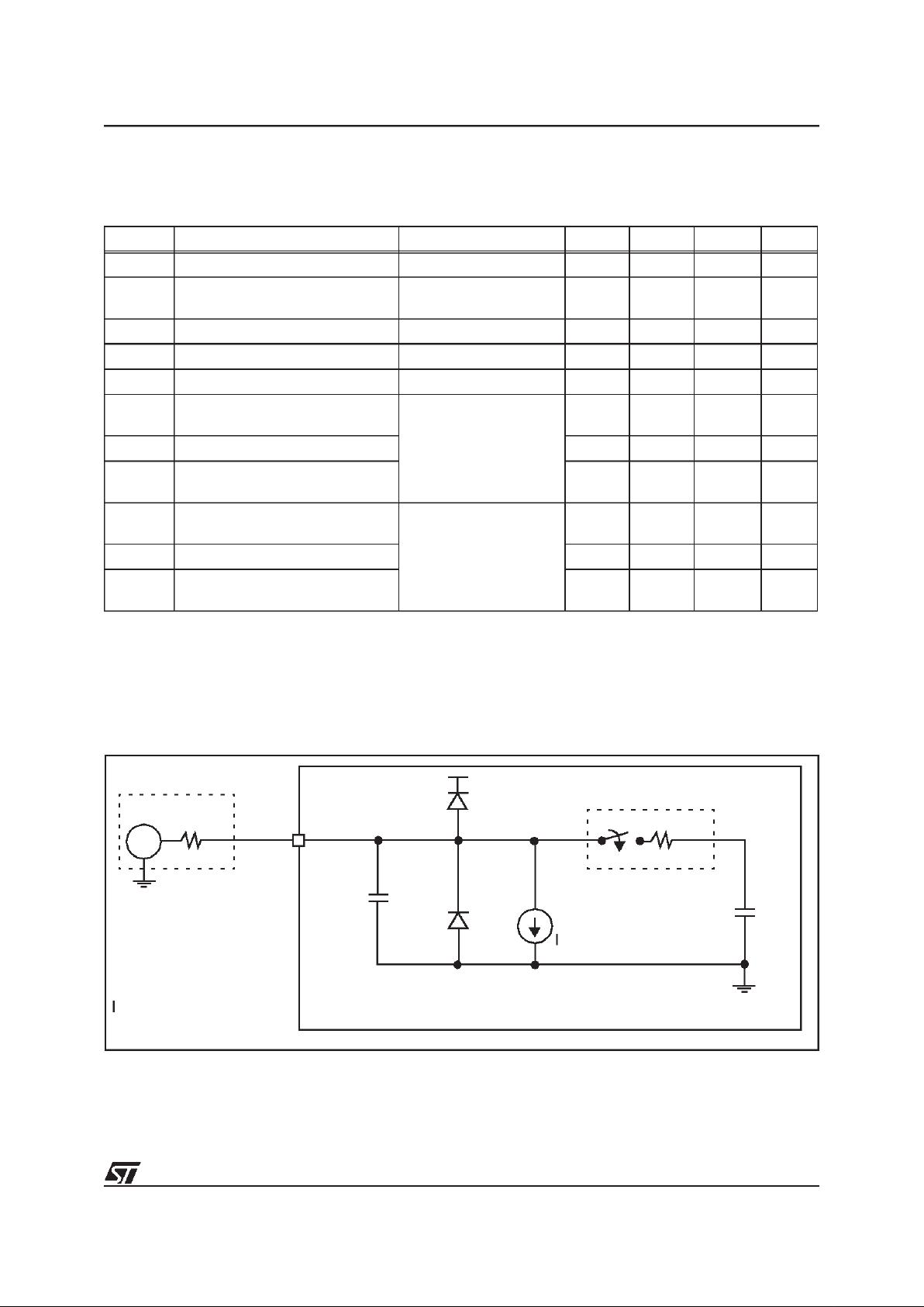
75/84
ST72101/ST72212/ST72213
6.6 A/D CONVERTER CHARACTERISTICS (ST72212 and ST72213 only)
(TA= -40°C to+125°C and VDD=5V±10% unlessotherwise specified )
*Note:
ADC Accuracyvs. Negative Injection Current
:
For I
inj-
=0.8mA, the typical leakageinduced inside the die is 1.6µA and theeffect on the ADC accuracy is
a lossof 1 LSB by 10KΩ increase of the external analog source impedance.
These measurement results and recommendations take worst case injection conditions into account:
- negative injection
- injectionto an Input with analogcapability, adjacent to the enabled Analog Input
-at5VVDDsupply, and worst case temperature.
Symbol Parameter Conditions Min Typ Max Unit
T
SAMPLE
Sample Duration 31.5 1/f
CPU
Res ADC Resolution
f
CPU
=8MHz
V
DD=VDDA
=5V
8 bit
DLE Differential Linearity Error* ±0.6 ±1
ILE Integral Linearity Error* ±2
V
AIN
Analog Input Voltage V
SSA
V
DDA
V
I
ADC
Supply current rise
during A/Dconversion
f
CPU
=8MHz
V
DD=VDDA
=5V
1mA
t
STAB
Stabilization timeafter ADC enable 30 µs
t
CONV
Conversion Time
8
64
µs
1/f
CPU
R
AIN
Resistance of analog sources
(V
AIN)
f
CPU
=8MHz, T=25°C,
V
DD=VDDA
=5V
15 ΚΩ
C
HOLD
Hold Capacitance 22 pF
R
SS
Resistance ofsampling switch and
internal trace
2 ΚΩ
Px.x/AINx
R
AIN
V
AIN
C
pin
5pF
V
DD
VT= 0.6V
leakage max.
V
T
= 0.6V
C
pin
V
T
leakage
C
hold
SS
Sampling
Switch
SS
R
SS
at the pin due
to various junctions
C
hold
22 pF
capacitance
= input capacitance
= threshold voltage
= sampling switch
= sample/hold
±1µA
V
SS
= leakage current
2ΚΩ
75
Page 76

76/84
ST72101/ST72212/ST72213
A/D CONVERTER CHARACTERISTICS (Cont’d)
Figure 42. ADC conversion characteristics
(2)
(1)
(3)
(4)
(5)
VR02133A
Offset Error OSE
Offset Error OSE
Gain Error GE
1 LSB(ideal)
1LSB
ideal
V
refPVrefM
–
256
--------------------------------------- -=
V
in(A)
(LSB
ideal
)
(1) Example of an actual transfer curve
(2) The ideal transfer curve
(3) Differential non-linearity error (DLE)
(4) Integral non-linearity error (ILE)
(5) Center of a step of the actual transfer curve
code
out
255
254
253
252
251
250
5
4
3
2
1
0
7
6
1 2 3 4 5 6 7 250 251252 253 254 255 256
76
Page 77

77/84
ST72101/ST72212/ST72213
6.7 SPI CHARACTERISTICS
Measurement points are VOL,VOH,VILand VIHin the SPI Timing Diagram
Figure 43. SPI Master Timing Diagram CPHA=0, CPOL=0
Serial Peripheral Interface
Ref. Symbol Parameter Condition
Value
Unit
Min. Max.
f
SPI
SPI frequency
Master
Slave
1/128
dc
1/4
1/2
f
CPU
1t
SPI
SPI clock period
Master
Slave
4
2
t
CPU
2t
Lead
Enable lead time Slave 120 ns
3t
Lag
Enable lag time Slave 120 ns
4t
SPI_H
Clock (SCK) high time
Master
Slave
100
90
ns
5t
SPI_L
Clock (SCK) low time
Master
Slave
100
90
ns
6t
SU
Data set-up time
Master
Slave
100
100
ns
7t
H
Data hold time (inputs)
Master
Slave
100
100
ns
8t
A
Access time (time to data active
from high impedance state)
Slave
0 120 ns
9t
Dis
Disable time (hold time to high impedance state)
240 ns
10 t
V
Data valid
Master (before capture edge)
Slave (after enableedge)
0.25
120
t
CPU
ns
11 t
Hold
Data hold time (outputs)
Master (before capture edge)
Slave (after enableedge)
0.25
0
t
CPU
ns
12 t
Rise
Rise time
(20% V
DD
to 70% VDD,CL=200pF)
Outputs: SCK,MOSI,MISO
Inputs: SCK,MOSI,MISO,SS
100
100
ns
µs
13 t
Fall
Fall time
(70% V
DD
to 20% VDD,CL=200pF)
Outputs: SCK,MOSI,MISO
Inputs: SCK,MOSI,MISO,SS
100
100
ns
µs
1
67
10 11
1213
SS
(INPUT)
SCK
(OUTPUT)
MISO
MOSI
(INPUT)
(OUTPUT)
4
5
D7-OUT D6-OUT D0-OUT
D7-IN D6-IN
D0-IN
VR000109
77
Page 78

78/84
ST72101/ST72212/ST72213
SPI CHARACTERISTICS (Cont’d)
Measurement points are VOL,VOH,VILand VIHin the SPI Timing Diagram
Figure 44. SPI Master Timing Diagram CPHA=0, CPOL=1
Figure 45. SPI Master Timing Diagram CPHA=1, CPOL=0
Figure 46. SPI Master Timing Diagram CPHA=1, CPOL=1
1
6
7
10 11
1213
SS
(INPUT)
SCK
(OUTPUT)
MISO
MOSI
(INPUT)
(OUTPUT)
45
VR000110
D7-OUT D6-OUT D0-OUT
D7-IN D6-IN
D0-IN
1
6
7
10 11
1213
SS
(INPUT)
SCK
(OUTPUT)
MISO
MOSI
(INPUT)
(OUTPUT)
54
VR000107
D7-IN
D6-IN D0-IN
D7-OUT D6-OUT
D0-OUT
1
6
7
10 11
12
13
SS
(INPUT)
SCK
(OUTPUT)
MISO
MOSI
(INPUT)
(OUTPUT)
4
5
VR000108
D7-OUT D6-OUT D0-OUT
D7-IN D6-IN
D0-IN
Page 79

79/84
ST72101/ST72212/ST72213
SPI CHARACTERISTICS (Cont’d)
Measurement points are VOL,VOH,VILand VIHin the SPI Timing Diagram
Figure 47. SPI Slave Timing Diagram CPHA=0, CPOL=0
Figure 48. SPI Slave Timing Diagram CPHA=0, CPOL=1
Figure 49. SPI Slave Timing Diagram CPHA=1, CPOL=0
Figure 50. SPI Slave Timing Diagram CPHA=1, CPOL=1
1
6
7
10
11
12
13
SS
(INPUT)
SCK
MISO
MOSI
(INPUT)
(OUTPUT)
5
4
(INPUT)
2
3
8
9
HIGH-Z
VR000113
D7-IN
D6-IN D0-IN
D7-OUT
D6-OUT D0-OUT
1
6
7
10 11
12
13
SS
(INPUT)
SCK
MISO
MOSI
(INPUT)
(OUTPUT)
54
(INPUT)
2
3
8
9
HIGH-Z
VR000114
D7-IN
D6-IN D0-IN
D7-OUT
D6-OUT D0-OUT
1
6
7
10
11
12
13
SS
(INPUT)
SCK
MISO
MOSI
(INPUT)
(OUTPUT)
54
(INPUT)
2
3
8 9
HIGH-Z
VR000111
D7-OUT
D6-OUT D0-OUT
D7-IN
D6-IN D0-IN
1
67
10
11
12 13
SS
(INPUT)
SCK
MISO
MOSI
(INPUT)
(OUTPUT)
54
(INPUT)
2
3
8
9
HIGH-Z
D7-OUT D6-OUT
D0-OUT
D7-IN D6-IN D0-IN
VR000112
Page 80
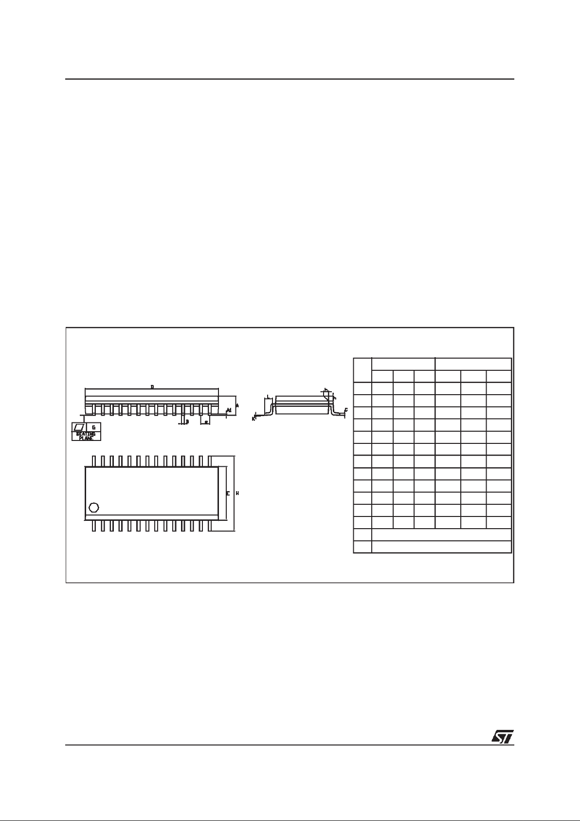
80/84
ST72101/ST72212/ST72213
7 GENERAL INFORMATION
7.1 EPROM ERASURE
EPROM version devices are erased by exposure
to high intensity UV light admitted through the
transparent window. This exposure discharges the
floating gate to its initial state through induced
photo current.
It is recommended that the EPROM devices be
kept out of direct sunlight, since the UV content of
sunlight can be sufficient to cause functional failure. Extended exposure to room level fluorescent
lighting mayalso cause erasure.
An opaque coating (paint, tape, label, etc...)
should be placed over the package window if the
product is to beoperated undertheselighting conditions. Covering the window also reduces IDDin
power-saving modes due to photo-diode leakage
currents.
An Ultraviolet source of wave length 2537 Å yielding a total integrated dosageof 15 Watt-sec/cm2is
required to erase the device. It will beerased in 15
to 20 minutes ifsuch aUV lamp with a 12mW/cm
2
power rating is placed 1 inch from the device window without any interposed filters.
7.2 PACKAGE MECHANICAL DATA
Figure 51. 28-Pin Small Outline Package, 300-mil Width
Dim.
mm inches
Min Typ Max Min Typ Max
A 2.35 2.65 0.0926 0.1043
A1 0.10 0.30 0.0040 0.0118
B 0.33 0.51 0.013 0.020
C 0.23 0.32 0.0091 0.0125
D 17.70 18.10 0.6969 0.7125
E 7.40 7.60 0.2914 0.2992
e 1.27 0.0500
H 10.01 10.64 0.394 0.419
h 0.25 0.74 0.010 0.029
K 0° 8°
L 0.41 1.27 0.016 0.050
G 0.10 0.004
Number of Pins
N28
SO28
Page 81

81/84
ST72101/ST72212/ST72213
Figure 52. 32-Pin Shrink Plastic Dual In Line Package
Figure 53. 32-Pin Shrink Ceramic Dual In-Line Package
1
N
b
D
VR01725J
N/2
b1
e
A
L
See Lead Detail
E
1
e
3
A
2
A
1
E
C
e
B
e
A
Dim.
mm inches
Min Typ Max Min Typ Max
A 3.56 3.76 5.08 0.140 0.148 0.200
A1 0.51 0.020
A2 3.05 3.56 4.57 0.120 0.140 0.180
b 0.36 0.46 0.58 0.014 0.018 0.023
b1 0.76 1.02 1.40 0.030 0.040 0.055
C 0.20 0.25 0.36 0.008 0.010 0.014
D 27.43 27.94 28.45 1.080 1.100 1.120
E 9.91 10.41 11.05 0.390 0.410 0.435
E1 7.62 8.89 9.40 0.300 0.350 0.370
e 1.78 0.070
eA 10.16 0.400
eB 12.70 0.500
L 2.54 3.05 3.81 0.100 0.120 0.150
Number of Pins
N32
CDIP32SW
Dim.
mm inches
Min Typ Max Min Typ Max
A 3.63 0.143
A1 0.38 0.015
B 0.36 0.46 0.58 0.014 0.018 0.023
B1 0.64 0.89 1.14 0.025 0.035 0.045
C 0.20 0.25 0.36 0.008 0.010 0.014
D 29.41 29.97 30.53 1.158 1.180 1.202
D1 26.67 1.050
E 10.16 0.400
E1 9.45 9.91 10.36 0.372 0.390 0.408
e 1.78 0.070
G 9.40 0.370
G1 14.73 0.580
G2 1.12 0.044
L 3.30 0.130
Ø 7.37 0.290
Number of Pins
N32
Page 82

82/84
ST72101/ST72212/ST72213
7.3 ORDERING INFORMATION
Each deviceis available forproduction in user programmable version (OTP) as well as in factory
coded version (ROM). OTPdevices areshipped to
customer with a default blank content FFh, while
ROM factory coded partscontain thecode sentby
customer. There is one common EPROM version
for debugging and prototyping which features the
maximum memory size and peripherals of the
family. Care must be taken to only use resources
available on the target device.
7.3.1 Transfer Of Customer Code
Customer code is made up of the ROM contents
and the list of the selected options (if any). The
ROM contents are to be sent on diskette, or by
electronic means,with thehexadecimal file in .S19
format generated by the development tool. All unused bytes must be set to FFh.
The selected options are communicated to STMicroelectronics using the correctly completed OPTION LIST appended.
The STMicroelectronics Sales Organization will be
pleased to provide detailed information on contractual points.
Figure 54. ROM Factory Coded Device Types
Figure 55. OTP User Programmable Device Types
Note: TheST72E251G2D0 (CERDIP 25 °C) is used as the EPROMversion for the above devices.
DEVICE
PACKAGE
TEMP.
RANGE
XXX/
Code name (defined by STMicroelectronics)
1 = standard 0 to +70°C
3 = automotive -40 to +125°C
6 = industrial -40 to +85°C
B = Plastic DIP
M = Plastic SOIC
ST72101G1
ST72101G2
ST72212G2
ST72213G1
DEVICE
PACKAGE
TEMP.
RANGE
Option (if any)
3 = automotive -40 to +125°C
6 = industrial -40 to +85°C
B = Plastic DIP
M = Plastic SOIC
ST72T101G1
ST72T101G2
ST72T212G2
ST72T213G1
XXX
Page 83

83/84
ST72101/ST72212/ST72213
ST72101, ST72213 and ST72212 MICROCONTROLLER OPTION LIST
Customer . . . .. . . . . . . .. . . . . . . . . . . . . . . ..
Address . . . . . . . . . . . .. . . . . . . . . . . . . . . . .
.............................
Contact . . . . . . . . . . . . . . . . . . . . . . . . .. . . .
Phone No . . . .. . . . . . . . . . . . . . . . . . . .. . . ..
Reference . . . . . . . . . . . .. . . . . . .. . . . . . . . . .
STMicroelectronics references
Device: [ ] ST72101 [ ] ST72212 [ ] ST72213
Package: [ ] Dual in Line Plastic [ ] Small OutlinePlastic with conditioning:
[ ] Standard (Stick)
[ ] Tape & Reel
Temperature Range: [ ] 0°Cto+70°C []-40°Cto+85°C[]-40°C to+ 125°C
Special Marking: [ ] No [ ] Yes ”_ _ _ _ _______”
Authorized characters are letters, digits, ’.’,’-’, ’/’ and spaces only.
Maximum character count: SDIP32: 10
SO28: 8
Comments:
Supply Operating Range in the application:
Oscillator Frequency in the application:
Notes . . . . . . . . . . . .. . . . . . .. . . . . . . . . .
Signature . . . . . . . . . . . .. . . . . . . . . . . . . . . . .
Date . . . .. . . . . . . .. . . . . . .. . . . . . . . . .
Page 84

84/84
ST72101/ST72212/ST72213
8 SUMMARY OF CHANGES
Information furnished is believed to be accurate and reliable. However, STMicroelectronics assumes no responsibility for the consequences
of useof such information nor for any infringement ofpatents orotherrights ofthird parties which may result from itsuse. No license isgranted
by implication or otherwise under any patent or patent rights of STMicroelectronics. Specifications mentioned in this publication are subject
to change without notice. This publication supersedes and replaces all information previously supplied. STMicroelectronics products are not
authorized for use as critical components in life support devices or systems without the express written approval of STMicroelectronics.
The ST logo is a registered trademark of STMicroelectronics
1999 STMicroelectronics - All Rights Reserved.
Purchase of I
2
C Components by STMicroelectronics conveys a license under the Philips I2C Patent. Rights to use these components in an
I
2
C system is granted provided that the system conforms to the I2C Standard Specification as defined by Philips.
STMicroelectronics Group of Companies
Australia - Brazil - China - Finland - France - Germany - Hong Kong -India - Italy - Japan - Malaysia - Malta - Morocco - Singapore - Spain
Sweden - Switzerland - United Kingdom - U.S.A.
http://www.st.com
Change Description (Rev. 1.5 to 1.6) Page
Added new External Connections section 9
Removed RP external resistor 16
Changed ORed to ANDed in External interrupts paragraph, to read “If several inputpins, con-
nected to the sameinterrupt vector, areconfigured asinterrupts, their signals are logically ANDed before entering the edge/level detection block”.
18 and 24
Added note ”Any modification ofone of these two bits resets the interrupt request related to
this interrupt vector.”
23
Added clamping diodes to I/O pin figure andtable 26
Added sections on low power modes and interrupts to peripheral descriptions 31,43,58,63
Changed 16-bit Timer Chapter 32 to 48
Added details to description of FOLV1 and FOLV2 bits 44
Added ADC recommended external connections 63
Added Reset characteristics section 74
Added figure to ADC electrical characteristics section 75
Change Description (Rev. 1.6 to 1.7)
SPR2 bit reinstated in SPI chapter 49 to 61
 Loading...