

ST72334xx-Auto,
ST72314xx-Auto, ST72124Jx-Auto
8-bit MCU for automotive with single voltage Flash/ROM memory,
ADC, 16-bit timers, SPI, SCI interfaces
■ Memories
– 8 or 16 Kbyte Program memory (ROM or sin-
gle voltage Flash) with readout protection and
in-situ programming (remote ISP)
– 256 bytes EEPROM Data memory (with read-
out protection option in ROM devices)
– 384 or 512 bytes RAM
■ Clock, Reset and Supply Management
– Enhanced reset system
– Enhanced low voltage supply supervisor with
3 programmable levels
– Clock sources: crystal/ceramic resonator os-
cillators or RC oscillators, external clock,
backup Clock Security System
– 4 Power Saving Modes: Halt, Active Halt,
Wait and Slow
– Beep and clock-out capabilities
■ Interrupt Management
– 10 interrupt vectors plus TRAP and RESET
– 15 external interrupt lines (4 vectors)
■ 44 or 32 I/O Ports
– 44 or 32 multifunctional bidirectional I/O lines:
– 21 or 19 alternate function lines
– 12 or 8 high sink outputs
■ 4 Timers
– Configurable watchdog timer
– Real-time base
– Two 16-bit timers with: 2 input captures (only
one on timer A), 2 output compares (only one
on timer A), External clock input on timer A,
PWM and Pulse generator modes
■ 2 Communications Interfaces
– SPI synchronous serial interface
– SCI asynchronous serial interface (LIN com-
■ 1 Analog Peripheral
– 8-bit ADC with 8 input channels (6 only on
■ Instruction Set
– 8-bit data manipulation
– 63 basic instructions
– 17 main addressing modes
– 8 x 8 unsigned multiply instruction
– True bit manipulation
■ Development Tools
– Full hardware/software development package
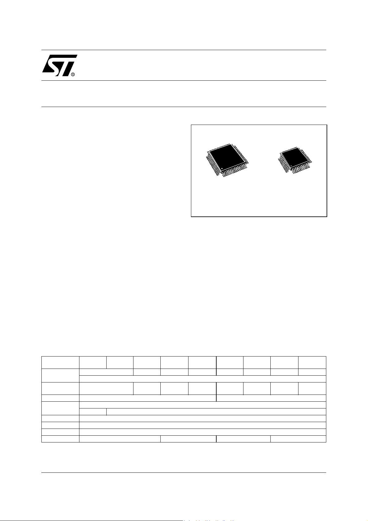
TQFP64
14 x 14
TQFP44
10 x 10
patible)
ST72334Jx, not available on ST72124J2)
Device Summary
Features
Prog. memory
RAM (stack) 384 (256) bytes
EEPROM - 256 bytes
Peripherals
Oper. Supply 3.2V to 5.5 V
CPU Freq. Up to 8 MHz (with up to 16 MHz oscillator)
Oper. Temp. -40°C to +85°C / -40°C to +125C° Flash or ROM (-40°C to +105°C ROM only)
Packages TQFP44 TQFP64 TQFP44 TQFP64
ST72124J2
-Auto
ST72314J2
-Auto
8 Kbytes 16 Kbytes 8 Kbytes 16 Kbytes 8 Kbytes 16 Kbytes 8 Kbytes 16 Kbytes
- ADC
ST72314J4
-Auto
512 (256)
bytes
ST72314N2
-Auto
384 (256)
bytes
Watchdog, Two 16-bit Timers, SPI, SCI
ST72314N4
-Auto
Flash/ROM
512 (256)
bytes
ST72334J2
-Auto
384 (256)
bytes
ST72334J4
-Auto
512 (256)
bytes
ST72334N2
-Auto
384 (256)
bytes
ST72334N4
-Auto
512 (256)
bytes
Rev. 1
October 2007 1/150
1

Table of Contents
1 PREAMBLE: ST72C334-Auto VERSUS ST72E331 SPECIFICATION . . . . . . . . . . . . . . . . . . . . 7
2 INTRODUCTION . . . . . . . . . . . . . . . . . . . . . . . . . . . . . . . . . . . . . . . . . . . . . . . . . . . . . . . . . . . . . . 8
3 PIN DESCRIPTION . . . . . . . . . . . . . . . . . . . . . . . . . . . . . . . . . . . . . . . . . . . . . . . . . . . . . . . . . . . . 9
4 REGISTER AND MEMORY MAP . . . . . . . . . . . . . . . . . . . . . . . . . . . . . . . . . . . . . . . . . . . . . . . . 14
5 FLASH PROGRAM MEMORY . . . . . . . . . . . . . . . . . . . . . . . . . . . . . . . . . . . . . . . . . . . . . . . . . . 18
5.1 INTRODUCTION . . . . . . . . . . . . . . . . . . . . . . . . . . . . . . . . . . . . . . . . . . . . . . . . . . . . . . . 18
5.2 MAIN FEATURES . . . . . . . . . . . . . . . . . . . . . . . . . . . . . . . . . . . . . . . . . . . . . . . . . . . . . . 18
5.3 STRUCTURAL ORGANIZATION . . . . . . . . . . . . . . . . . . . . . . . . . . . . . . . . . . . . . . . . . . 18
5.4 IN-SITU PROGRAMMING (ISP) MODE . . . . . . . . . . . . . . . . . . . . . . . . . . . . . . . . . . . . . 18
5.5 MEMORY READOUT PROTECTION . . . . . . . . . . . . . . . . . . . . . . . . . . . . . . . . . . . . . . . 18
6 DATA EEPROM . . . . . . . . . . . . . . . . . . . . . . . . . . . . . . . . . . . . . . . . . . . . . . . . . . . . . . . . . . . . . 19
6.1 INTRODUCTION . . . . . . . . . . . . . . . . . . . . . . . . . . . . . . . . . . . . . . . . . . . . . . . . . . . . . . . 19
6.2 MAIN FEATURES . . . . . . . . . . . . . . . . . . . . . . . . . . . . . . . . . . . . . . . . . . . . . . . . . . . . . . 19
6.3 MEMORY ACCESS . . . . . . . . . . . . . . . . . . . . . . . . . . . . . . . . . . . . . . . . . . . . . . . . . . . . . 20
6.4 POWER SAVING MODES . . . . . . . . . . . . . . . . . . . . . . . . . . . . . . . . . . . . . . . . . . . . . . . 21
6.5 ACCESS ERROR HANDLING . . . . . . . . . . . . . . . . . . . . . . . . . . . . . . . . . . . . . . . . . . . . 21
6.6 REGISTER DESCRIPTION . . . . . . . . . . . . . . . . . . . . . . . . . . . . . . . . . . . . . . . . . . . . . . . 22
6.7 READOUT PROTECTION OPTION . . . . . . . . . . . . . . . . . . . . . . . . . . . . . . . . . . . . . . . . 22
7 CENTRAL PROCESSING UNIT . . . . . . . . . . . . . . . . . . . . . . . . . . . . . . . . . . . . . . . . . . . . . . . . . 23
7.1 INTRODUCTION . . . . . . . . . . . . . . . . . . . . . . . . . . . . . . . . . . . . . . . . . . . . . . . . . . . . . . . 23
7.2 MAIN FEATURES . . . . . . . . . . . . . . . . . . . . . . . . . . . . . . . . . . . . . . . . . . . . . . . . . . . . . . 23
7.3 CPU REGISTERS . . . . . . . . . . . . . . . . . . . . . . . . . . . . . . . . . . . . . . . . . . . . . . . . . . . . . . 23
8 SUPPLY, RESET AND CLOCK MANAGEMENT . . . . . . . . . . . . . . . . . . . . . . . . . . . . . . . . . . . . 26
8.1 LOW VOLTAGE DETECTOR (LVD) . . . . . . . . . . . . . . . . . . . . . . . . . . . . . . . . . . . . . . . . 27
8.2 RESET SEQUENCE MANAGER (RSM) . . . . . . . . . . . . . . . . . . . . . . . . . . . . . . . . . . . . . 28
8.2.1 Introduction . . . . . . . . . . . . . . . . . . . . . . . . . . . . . . . . . . . . . . . . . . . . . . . . . . . . . . . 28
8.2.2 Asynchronous External RESET Pin . . . . . . . . . . . . . . . . . . . . . . . . . . . . . . . . . . . . . 29
8.2.3 Internal Low Voltage Detection RESET . . . . . . . . . . . . . . . . . . . . . . . . . . . . . . . . . . 29
8.2.4 Internal Watchdog RESET . . . . . . . . . . . . . . . . . . . . . . . . . . . . . . . . . . . . . . . . . . . . 29
8.3 MULTI-OSCILLATOR (MO) . . . . . . . . . . . . . . . . . . . . . . . . . . . . . . . . . . . . . . . . . . . . . . . 30
8.4 CLOCK SECURITY SYSTEM (CSS) . . . . . . . . . . . . . . . . . . . . . . . . . . . . . . . . . . . . . . . . 32
8.4.1 Clock Filter Control . . . . . . . . . . . . . . . . . . . . . . . . . . . . . . . . . . . . . . . . . . . . . . . . . 32
8.4.2 Safe Oscillator Control . . . . . . . . . . . . . . . . . . . . . . . . . . . . . . . . . . . . . . . . . . . . . . . 32
8.4.3 Low Power Modes . . . . . . . . . . . . . . . . . . . . . . . . . . . . . . . . . . . . . . . . . . . . . . . . . 32
8.4.4 Interrupts . . . . . . . . . . . . . . . . . . . . . . . . . . . . . . . . . . . . . . . . . . . . . . . . . . . . . . . . . 32
8.5 SUPPLY, RESET AND CLOCK REGISTER DESCRIPTION . . . . . . . . . . . . . . . . . . . . . 33
9 INTERRUPTS . . . . . . . . . . . . . . . . . . . . . . . . . . . . . . . . . . . . . . . . . . . . . . . . . . . . . . . . . . . . . . . 34
9.1 NON-MASKABLE SOFTWARE INTERRUPT . . . . . . . . . . . . . . . . . . . . . . . . . . . . . . . . . 34
9.2 EXTERNAL INTERRUPTS . . . . . . . . . . . . . . . . . . . . . . . . . . . . . . . . . . . . . . . . . . . . . . . 34
9.3 PERIPHERAL INTERRUPTS . . . . . . . . . . . . . . . . . . . . . . . . . . . . . . . . . . . . . . . . . . . . . 34
10 POWER SAVING MODES . . . . . . . . . . . . . . . . . . . . . . . . . . . . . . . . . . . . . . . . . . . . . . . . . . . . 36
10.1 INTRODUCTION . . . . . . . . . . . . . . . . . . . . . . . . . . . . . . . . . . . . . . . . . . . . . . . . . . . . . . . 36
10.2 SLOW MODE . . . . . . . . . . . . . . . . . . . . . . . . . . . . . . . . . . . . . . . . . . . . . . . . . . . . . . . . . 36
150
2/150
2

Table of Contents
10.3 WAIT MODE . . . . . . . . . . . . . . . . . . . . . . . . . . . . . . . . . . . . . . . . . . . . . . . . . . . . . . . . . . 37
10.4 ACTIVE HALT AND HALT MODES . . . . . . . . . . . . . . . . . . . . . . . . . . . . . . . . . . . . . . . . . 38
10.4.1Active Halt Mode . . . . . . . . . . . . . . . . . . . . . . . . . . . . . . . . . . . . . . . . . . . . . . . . . . . 38
10.4.2Halt Mode . . . . . . . . . . . . . . . . . . . . . . . . . . . . . . . . . . . . . . . . . . . . . . . . . . . . . . . . . 39
11 I/O PORTS . . . . . . . . . . . . . . . . . . . . . . . . . . . . . . . . . . . . . . . . . . . . . . . . . . . . . . . . . . . . . . . . . 40
11.1 INTRODUCTION . . . . . . . . . . . . . . . . . . . . . . . . . . . . . . . . . . . . . . . . . . . . . . . . . . . . . . . 40
11.2 FUNCTIONAL DESCRIPTION . . . . . . . . . . . . . . . . . . . . . . . . . . . . . . . . . . . . . . . . . . . . 40
11.2.1Input Modes . . . . . . . . . . . . . . . . . . . . . . . . . . . . . . . . . . . . . . . . . . . . . . . . . . . . . . . 40
11.2.2Output Modes . . . . . . . . . . . . . . . . . . . . . . . . . . . . . . . . . . . . . . . . . . . . . . . . . . . . . 40
11.2.3Alternate Functions . . . . . . . . . . . . . . . . . . . . . . . . . . . . . . . . . . . . . . . . . . . . . . . . . 40
11.3 I/O PORT IMPLEMENTATION . . . . . . . . . . . . . . . . . . . . . . . . . . . . . . . . . . . . . . . . . . . . 43
11.4 LOW POWER MODES . . . . . . . . . . . . . . . . . . . . . . . . . . . . . . . . . . . . . . . . . . . . . . . . . . 44
11.5 INTERRUPTS . . . . . . . . . . . . . . . . . . . . . . . . . . . . . . . . . . . . . . . . . . . . . . . . . . . . . . . . . 44
11.5.1Register Description . . . . . . . . . . . . . . . . . . . . . . . . . . . . . . . . . . . . . . . . . . . . . . . . . 45
12 MISCELLANEOUS REGISTERS . . . . . . . . . . . . . . . . . . . . . . . . . . . . . . . . . . . . . . . . . . . . . . . 47
12.1 I/O PORT INTERRUPT SENSITIVITY . . . . . . . . . . . . . . . . . . . . . . . . . . . . . . . . . . . . . . 47
12.2 I/O PORT ALTERNATE FUNCTIONS . . . . . . . . . . . . . . . . . . . . . . . . . . . . . . . . . . . . . . . 47
12.3 REGISTERS DESCRIPTION . . . . . . . . . . . . . . . . . . . . . . . . . . . . . . . . . . . . . . . . . . . . . 48
13 ON-CHIP PERIPHERALS . . . . . . . . . . . . . . . . . . . . . . . . . . . . . . . . . . . . . . . . . . . . . . . . . . . . . 50
13.1 WATCHDOG TIMER (WDG) . . . . . . . . . . . . . . . . . . . . . . . . . . . . . . . . . . . . . . . . . . . . . . 50
13.1.1Introduction . . . . . . . . . . . . . . . . . . . . . . . . . . . . . . . . . . . . . . . . . . . . . . . . . . . . . . . 50
13.1.2Main Features . . . . . . . . . . . . . . . . . . . . . . . . . . . . . . . . . . . . . . . . . . . . . . . . . . . . . 50
13.1.3Functional Description . . . . . . . . . . . . . . . . . . . . . . . . . . . . . . . . . . . . . . . . . . . . . . . 50
13.1.4Hardware Watchdog Option . . . . . . . . . . . . . . . . . . . . . . . . . . . . . . . . . . . . . . . . . . . 51
13.1.5Low Power Modes . . . . . . . . . . . . . . . . . . . . . . . . . . . . . . . . . . . . . . . . . . . . . . . . . . 51
13.1.6Interrupts . . . . . . . . . . . . . . . . . . . . . . . . . . . . . . . . . . . . . . . . . . . . . . . . . . . . . . . . . 51
13.1.7Register Description . . . . . . . . . . . . . . . . . . . . . . . . . . . . . . . . . . . . . . . . . . . . . . . . . 51
13.2 MAIN CLOCK CONTROLLER WITH REAL-TIME CLOCK TIMER (MCC/RTC) . . . . . . . 53
13.2.1Programmable CPU clock prescaler . . . . . . . . . . . . . . . . . . . . . . . . . . . . . . . . . . . . 53
13.2.2Clock-out capability . . . . . . . . . . . . . . . . . . . . . . . . . . . . . . . . . . . . . . . . . . . . . . . . . 53
13.2.3Real-time clock timer (RTC) . . . . . . . . . . . . . . . . . . . . . . . . . . . . . . . . . . . . . . . . . . . 53
13.2.4Low Power Modes . . . . . . . . . . . . . . . . . . . . . . . . . . . . . . . . . . . . . . . . . . . . . . . . . 54
13.2.5Interrupts . . . . . . . . . . . . . . . . . . . . . . . . . . . . . . . . . . . . . . . . . . . . . . . . . . . . . . . . . 54
13.3 16-BIT TIMER . . . . . . . . . . . . . . . . . . . . . . . . . . . . . . . . . . . . . . . . . . . . . . . . . . . . . . . . . 55
13.3.1Introduction . . . . . . . . . . . . . . . . . . . . . . . . . . . . . . . . . . . . . . . . . . . . . . . . . . . . . . . 55
13.3.2Main Features . . . . . . . . . . . . . . . . . . . . . . . . . . . . . . . . . . . . . . . . . . . . . . . . . . . . . 55
13.3.3Functional Description . . . . . . . . . . . . . . . . . . . . . . . . . . . . . . . . . . . . . . . . . . . . . . . 55
13.3.4Low Power Modes . . . . . . . . . . . . . . . . . . . . . . . . . . . . . . . . . . . . . . . . . . . . . . . . . 67
13.3.5Interrupts . . . . . . . . . . . . . . . . . . . . . . . . . . . . . . . . . . . . . . . . . . . . . . . . . . . . . . . . . 67
13.3.6Summary of Timer modes . . . . . . . . . . . . . . . . . . . . . . . . . . . . . . . . . . . . . . . . . . . . 67
13.3.7Register Description . . . . . . . . . . . . . . . . . . . . . . . . . . . . . . . . . . . . . . . . . . . . . . . . . 68
13.4 SERIAL PERIPHERAL INTERFACE (SPI) . . . . . . . . . . . . . . . . . . . . . . . . . . . . . . . . . . . 73
13.4.1Introduction . . . . . . . . . . . . . . . . . . . . . . . . . . . . . . . . . . . . . . . . . . . . . . . . . . . . . . . 73
13.4.2Main Features . . . . . . . . . . . . . . . . . . . . . . . . . . . . . . . . . . . . . . . . . . . . . . . . . . . . . 73
13.4.3General description . . . . . . . . . . . . . . . . . . . . . . . . . . . . . . . . . . . . . . . . . . . . . . . . . 73
13.4.4Functional Description . . . . . . . . . . . . . . . . . . . . . . . . . . . . . . . . . . . . . . . . . . . . . . . 75
3/150
3

ST72334xx-Auto, ST72314xx-Auto, ST72124Jx-Auto
13.4.5Low Power Modes . . . . . . . . . . . . . . . . . . . . . . . . . . . . . . . . . . . . . . . . . . . . . . . . . . 82
13.4.6Interrupts . . . . . . . . . . . . . . . . . . . . . . . . . . . . . . . . . . . . . . . . . . . . . . . . . . . . . . . . . 82
13.4.7Register Description . . . . . . . . . . . . . . . . . . . . . . . . . . . . . . . . . . . . . . . . . . . . . . . . . 83
13.5 SERIAL COMMUNICATIONS INTERFACE (SCI) . . . . . . . . . . . . . . . . . . . . . . . . . . . . . . 86
13.5.1Introduction . . . . . . . . . . . . . . . . . . . . . . . . . . . . . . . . . . . . . . . . . . . . . . . . . . . . . . . 86
13.5.2Main Features . . . . . . . . . . . . . . . . . . . . . . . . . . . . . . . . . . . . . . . . . . . . . . . . . . . . . 86
13.5.3General Description . . . . . . . . . . . . . . . . . . . . . . . . . . . . . . . . . . . . . . . . . . . . . . . . . 86
13.5.4LIN Protocol support . . . . . . . . . . . . . . . . . . . . . . . . . . . . . . . . . . . . . . . . . . . . . . . . 86
13.5.5Functional Description . . . . . . . . . . . . . . . . . . . . . . . . . . . . . . . . . . . . . . . . . . . . . . . 88
13.5.6Low Power Modes . . . . . . . . . . . . . . . . . . . . . . . . . . . . . . . . . . . . . . . . . . . . . . . . . . 93
13.5.7Interrupts . . . . . . . . . . . . . . . . . . . . . . . . . . . . . . . . . . . . . . . . . . . . . . . . . . . . . . . . . 93
13.5.8Register Description . . . . . . . . . . . . . . . . . . . . . . . . . . . . . . . . . . . . . . . . . . . . . . . . . 94
13.6 8-BIT A/D CONVERTER (ADC) . . . . . . . . . . . . . . . . . . . . . . . . . . . . . . . . . . . . . . . . . . . 98
13.6.1Introduction . . . . . . . . . . . . . . . . . . . . . . . . . . . . . . . . . . . . . . . . . . . . . . . . . . . . . . . 98
13.6.2Main Features . . . . . . . . . . . . . . . . . . . . . . . . . . . . . . . . . . . . . . . . . . . . . . . . . . . . . 98
13.6.3Functional Description . . . . . . . . . . . . . . . . . . . . . . . . . . . . . . . . . . . . . . . . . . . . . . . 98
13.6.4Low Power Modes . . . . . . . . . . . . . . . . . . . . . . . . . . . . . . . . . . . . . . . . . . . . . . . . . 99
13.6.5Interrupts . . . . . . . . . . . . . . . . . . . . . . . . . . . . . . . . . . . . . . . . . . . . . . . . . . . . . . . . . 99
13.6.6Register Description . . . . . . . . . . . . . . . . . . . . . . . . . . . . . . . . . . . . . . . . . . . . . . . . 100
14 INSTRUCTION SET . . . . . . . . . . . . . . . . . . . . . . . . . . . . . . . . . . . . . . . . . . . . . . . . . . . . . . . . 102
14.1 ST7 ADDRESSING MODES . . . . . . . . . . . . . . . . . . . . . . . . . . . . . . . . . . . . . . . . . . . . . 102
14.1.1Inherent . . . . . . . . . . . . . . . . . . . . . . . . . . . . . . . . . . . . . . . . . . . . . . . . . . . . . . . . . 103
14.1.2Immediate . . . . . . . . . . . . . . . . . . . . . . . . . . . . . . . . . . . . . . . . . . . . . . . . . . . . . . . 103
14.1.3Direct . . . . . . . . . . . . . . . . . . . . . . . . . . . . . . . . . . . . . . . . . . . . . . . . . . . . . . . . . . . 103
14.1.4Indexed (No Offset, Short, Long) . . . . . . . . . . . . . . . . . . . . . . . . . . . . . . . . . . . . . . 103
14.1.5Indirect (Short, Long) . . . . . . . . . . . . . . . . . . . . . . . . . . . . . . . . . . . . . . . . . . . . . . . 103
14.1.6Indirect Indexed (Short, Long) . . . . . . . . . . . . . . . . . . . . . . . . . . . . . . . . . . . . . . . . 104
14.1.7Relative Mode (Direct, Indirect) . . . . . . . . . . . . . . . . . . . . . . . . . . . . . . . . . . . . . . . 104
14.2 INSTRUCTION GROUPS . . . . . . . . . . . . . . . . . . . . . . . . . . . . . . . . . . . . . . . . . . . . . . . 105
15 ELECTRICAL CHARACTERISTICS . . . . . . . . . . . . . . . . . . . . . . . . . . . . . . . . . . . . . . . . . . . . 108
15.1 PARAMETER CONDITIONS . . . . . . . . . . . . . . . . . . . . . . . . . . . . . . . . . . . . . . . . . . . . . 108
15.1.1Minimum and Maximum values . . . . . . . . . . . . . . . . . . . . . . . . . . . . . . . . . . . . . . . 108
15.1.2Typical values . . . . . . . . . . . . . . . . . . . . . . . . . . . . . . . . . . . . . . . . . . . . . . . . . . . . 108
15.1.3Typical curves . . . . . . . . . . . . . . . . . . . . . . . . . . . . . . . . . . . . . . . . . . . . . . . . . . . . 108
15.1.4Loading capacitor . . . . . . . . . . . . . . . . . . . . . . . . . . . . . . . . . . . . . . . . . . . . . . . . . . 108
15.1.5Pin input voltage . . . . . . . . . . . . . . . . . . . . . . . . . . . . . . . . . . . . . . . . . . . . . . . . . . 108
15.2 ABSOLUTE MAXIMUM RATINGS . . . . . . . . . . . . . . . . . . . . . . . . . . . . . . . . . . . . . . . . 109
15.2.1Voltage Characteristics . . . . . . . . . . . . . . . . . . . . . . . . . . . . . . . . . . . . . . . . . . . . . 109
15.2.2Current Characteristics . . . . . . . . . . . . . . . . . . . . . . . . . . . . . . . . . . . . . . . . . . . . . 109
15.2.3Thermal Characteristics . . . . . . . . . . . . . . . . . . . . . . . . . . . . . . . . . . . . . . . . . . . . 110
15.3 OPERATING CONDITIONS . . . . . . . . . . . . . . . . . . . . . . . . . . . . . . . . . . . . . . . . . . . . . 111
15.3.1General Operating Conditions . . . . . . . . . . . . . . . . . . . . . . . . . . . . . . . . . . . . . . . 111
15.3.2Operating Conditions with Low Voltage Detector (LVD) . . . . . . . . . . . . . . . . . . . . 112
15.4 SUPPLY CURRENT CHARACTERISTICS . . . . . . . . . . . . . . . . . . . . . . . . . . . . . . . . . . 114
15.4.1Run and Slow Modes . . . . . . . . . . . . . . . . . . . . . . . . . . . . . . . . . . . . . . . . . . . . . . 114
15.4.2Wait and Slow Wait Modes . . . . . . . . . . . . . . . . . . . . . . . . . . . . . . . . . . . . . . . . . . 115
15.4.3Halt and Active Halt Modes . . . . . . . . . . . . . . . . . . . . . . . . . . . . . . . . . . . . . . . . . . 116
4/150

ST72334xx-Auto, ST72314xx-Auto, ST72124Jx-Auto
15.4.4Supply and Clock Managers . . . . . . . . . . . . . . . . . . . . . . . . . . . . . . . . . . . . . . . . . 116
15.4.5On-Chip Peripherals . . . . . . . . . . . . . . . . . . . . . . . . . . . . . . . . . . . . . . . . . . . . . . . 116
15.5 CLOCK AND TIMING CHARACTERISTICS . . . . . . . . . . . . . . . . . . . . . . . . . . . . . . . . . 117
15.5.1General Timings . . . . . . . . . . . . . . . . . . . . . . . . . . . . . . . . . . . . . . . . . . . . . . . . . . 117
15.5.2External Clock Source . . . . . . . . . . . . . . . . . . . . . . . . . . . . . . . . . . . . . . . . . . . . . 117
15.5.3Crystal and Ceramic Resonator Oscillators . . . . . . . . . . . . . . . . . . . . . . . . . . . . . . 118
15.5.4RC Oscillators . . . . . . . . . . . . . . . . . . . . . . . . . . . . . . . . . . . . . . . . . . . . . . . . . . . . 121
15.5.5Clock Security System (CSS) . . . . . . . . . . . . . . . . . . . . . . . . . . . . . . . . . . . . . . . . 122
15.6 MEMORY CHARACTERISTICS . . . . . . . . . . . . . . . . . . . . . . . . . . . . . . . . . . . . . . . . . . 123
15.6.1RAM and Hardware Registers . . . . . . . . . . . . . . . . . . . . . . . . . . . . . . . . . . . . . . . 123
15.6.2EEPROM Data Memory . . . . . . . . . . . . . . . . . . . . . . . . . . . . . . . . . . . . . . . . . . . . 123
15.6.3Flash Program Memory . . . . . . . . . . . . . . . . . . . . . . . . . . . . . . . . . . . . . . . . . . . . 123
15.7 EMC CHARACTERISTICS . . . . . . . . . . . . . . . . . . . . . . . . . . . . . . . . . . . . . . . . . . . . . . 124
15.7.1Functional EMS . . . . . . . . . . . . . . . . . . . . . . . . . . . . . . . . . . . . . . . . . . . . . . . . . . . 124
15.7.2Absolute Electrical Sensitivity . . . . . . . . . . . . . . . . . . . . . . . . . . . . . . . . . . . . . . . . 125
15.7.3ESD Pin Protection Strategy . . . . . . . . . . . . . . . . . . . . . . . . . . . . . . . . . . . . . . . . . 127
15.8 I/O PORT PIN CHARACTERISTICS . . . . . . . . . . . . . . . . . . . . . . . . . . . . . . . . . . . . . . . 129
15.8.1General Characteristics . . . . . . . . . . . . . . . . . . . . . . . . . . . . . . . . . . . . . . . . . . . . . 129
15.8.2Output Driving Current . . . . . . . . . . . . . . . . . . . . . . . . . . . . . . . . . . . . . . . . . . . . . . 130
15.9 CONTROL PIN CHARACTERISTICS . . . . . . . . . . . . . . . . . . . . . . . . . . . . . . . . . . . . . . 132
15.9.1Asynchronous RESET Pin . . . . . . . . . . . . . . . . . . . . . . . . . . . . . . . . . . . . . . . . . . . 132
15.9.2ISPSEL Pin . . . . . . . . . . . . . . . . . . . . . . . . . . . . . . . . . . . . . . . . . . . . . . . . . . . . . . 134
15.10 TIMER PERIPHERAL CHARACTERISTICS . . . . . . . . . . . . . . . . . . . . . . . . . . . . . . . . . 135
15.10.1Watchdog Timer . . . . . . . . . . . . . . . . . . . . . . . . . . . . . . . . . . . . . . . . . . . . . . . . . 135
15.10.216-Bit Timer . . . . . . . . . . . . . . . . . . . . . . . . . . . . . . . . . . . . . . . . . . . . . . . . . . . . . 135
15.11 COMMUNICATION INTERFACE CHARACTERISTICS . . . . . . . . . . . . . . . . . . . . . . . . 136
15.11.1SPI - Serial Peripheral Interface . . . . . . . . . . . . . . . . . . . . . . . . . . . . . . . . . . . . . . 136
15.11.2SCI - Serial Communications Interface . . . . . . . . . . . . . . . . . . . . . . . . . . . . . . . . 138
15.12 8-BIT ADC CHARACTERISTICS . . . . . . . . . . . . . . . . . . . . . . . . . . . . . . . . . . . . . . . . . 139
16 PACKAGE CHARACTERISTICS . . . . . . . . . . . . . . . . . . . . . . . . . . . . . . . . . . . . . . . . . . . . . . 141
16.1 PACKAGE MECHANICAL DATA . . . . . . . . . . . . . . . . . . . . . . . . . . . . . . . . . . . . . . . . . 141
16.2 THERMAL CHARACTERISTICS . . . . . . . . . . . . . . . . . . . . . . . . . . . . . . . . . . . . . . . . . . 142
16.3 ECOPACK® . . . . . . . . . . . . . . . . . . . . . . . . . . . . . . . . . . . . . . . . . . . . . . . . . . . . . . . . . 142
17 DEVICE CONFIGURATION AND ORDERING INFORMATION . . . . . . . . . . . . . . . . . . . . . . . 143
17.1 INTRODUCTION . . . . . . . . . . . . . . . . . . . . . . . . . . . . . . . . . . . . . . . . . . . . . . . . . . . . . . 143
17.2 OPTION BYTES . . . . . . . . . . . . . . . . . . . . . . . . . . . . . . . . . . . . . . . . . . . . . . . . . . . . . . 143
17.2.1User Option Byte 0 . . . . . . . . . . . . . . . . . . . . . . . . . . . . . . . . . . . . . . . . . . . . . . . . . 143
17.2.2User Option Byte 1 . . . . . . . . . . . . . . . . . . . . . . . . . . . . . . . . . . . . . . . . . . . . . . . . . 143
17.3 TRANSFER OF CUSTOMER CODE . . . . . . . . . . . . . . . . . . . . . . . . . . . . . . . . . . . . . . 144
17.4 DEVELOPMENT TOOLS . . . . . . . . . . . . . . . . . . . . . . . . . . . . . . . . . . . . . . . . . . . . . . . 146
17.4.1Suggested List of Socket Types . . . . . . . . . . . . . . . . . . . . . . . . . . . . . . . . . . . . . . 147
17.5 ST7 APPLICATION NOTES . . . . . . . . . . . . . . . . . . . . . . . . . . . . . . . . . . . . . . . . . . . . . 147
18 IMPORTANT NOTES . . . . . . . . . . . . . . . . . . . . . . . . . . . . . . . . . . . . . . . . . . . . . . . . . . . . . . . 148
18.1 SCI BAUD RATE REGISTERS . . . . . . . . . . . . . . . . . . . . . . . . . . . . . . . . . . . . . . . . . . . 148
19 SUMMARY OF CHANGES . . . . . . . . . . . . . . . . . . . . . . . . . . . . . . . . . . . . . . . . . . . . . . . . . . . 149
5/150

ST72334xx-Auto, ST72314xx-Auto, ST72124Jx-Auto
To obtain the most recent version of this datasheet,
please check at www.st.com>products>technical literature>datasheet.
Please also pay special attention to the Section “IMPORTANT NOTES” on page 148
6/150

ST72334xx-Auto, ST72314xx-Auto, ST72124Jx-Auto
1 PREAMBLE: ST72C334-Auto VERSUS ST72E331 SPECIFICATION
New Features available on the ST72C334-Auto
■ 8 or 16K Flash/ROM with In-Situ Programming
and Readout protection
■ New ADC with a better accuracy and conversion
time
■ New configurable Clock, Reset and Supply
system
■ New power saving mode with real-time base:
Active Halt
■ Beep capability on PF1
■ New interrupt source: Clock security system
(CSS) or Main clock controller (MCC)
ST72C334-Auto I/O Configuration and Pinout
■ Same pinout as ST72E331
■ PA6 and PA7 are true open drain I/O ports
without pull-up (same as ST72E331)
■ PA3, PB3, PB4 and PF2 have no pull-up
configuration (all I/Os present on TQFP44)
■ PA5:4, PC3:2, PE7:4 and PF7:6 have high sink
capabilities (20mA on N-buffer, 2mA on P-buffer
and pull-up). On the ST72E331, all these pads
(except PA5:4) were 2mA push-pull pads
without high sink capabilities. PA4 and PA5
were 20mA true open drains.
New Memory Locations in ST72C334-Auto
■ 20h: MISCR register becomes MISCR1 register
(naming change)
■ 29h: new control/status register for the MCC
module
■ 2Bh: new control/status register for the Clock,
Reset and Supply control. This register replaces
the WDGSR register keeping the WDOGF flag
compatibility.
■ 40h: new MISCR2 register
7/150
ST72334xx-Auto, ST72314xx-Auto, ST72124Jx-Auto
2 INTRODUCTION
The ST72334J/N-Auto, ST72314J/N-Auto and
ST72124J-Auto devices are members of the ST7
microcontroller family. They can be grouped as fol
lows:
– ST72334J/N-Auto devices are designed for mid-
range applications with Data EEPROM, ADC,
SPI and SCI interface capabilities.
– ST72314J/N-Auto devices target the same
range of applications but without Data EEPROM.
– ST72124J-Auto devices are for applications that
do not need Data EEPROM and the ADC periph
eral.
All devices are based on a common industrystandard 8-bit core, featuring an enhanced instruc
tion set.
The ST72C334J/N-Auto, ST72C314J/N-Auto and
ST72C124J-Auto versions feature single-voltage
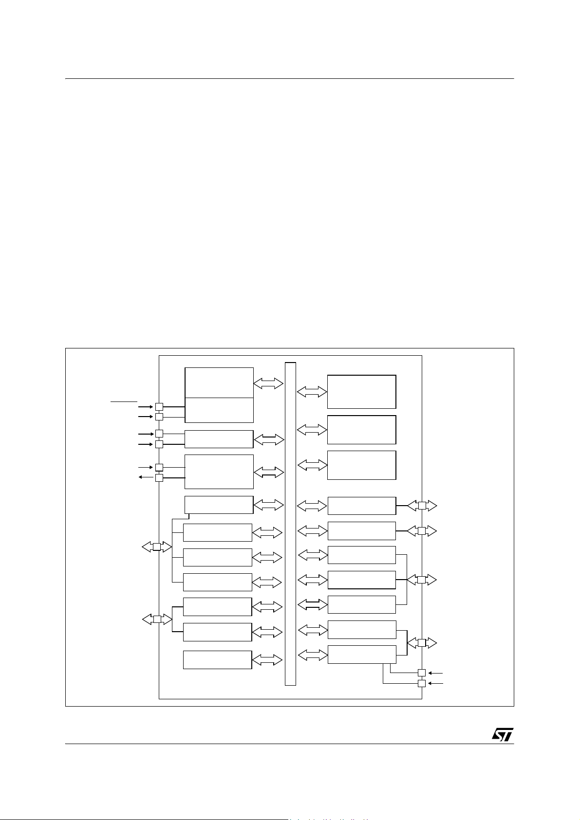
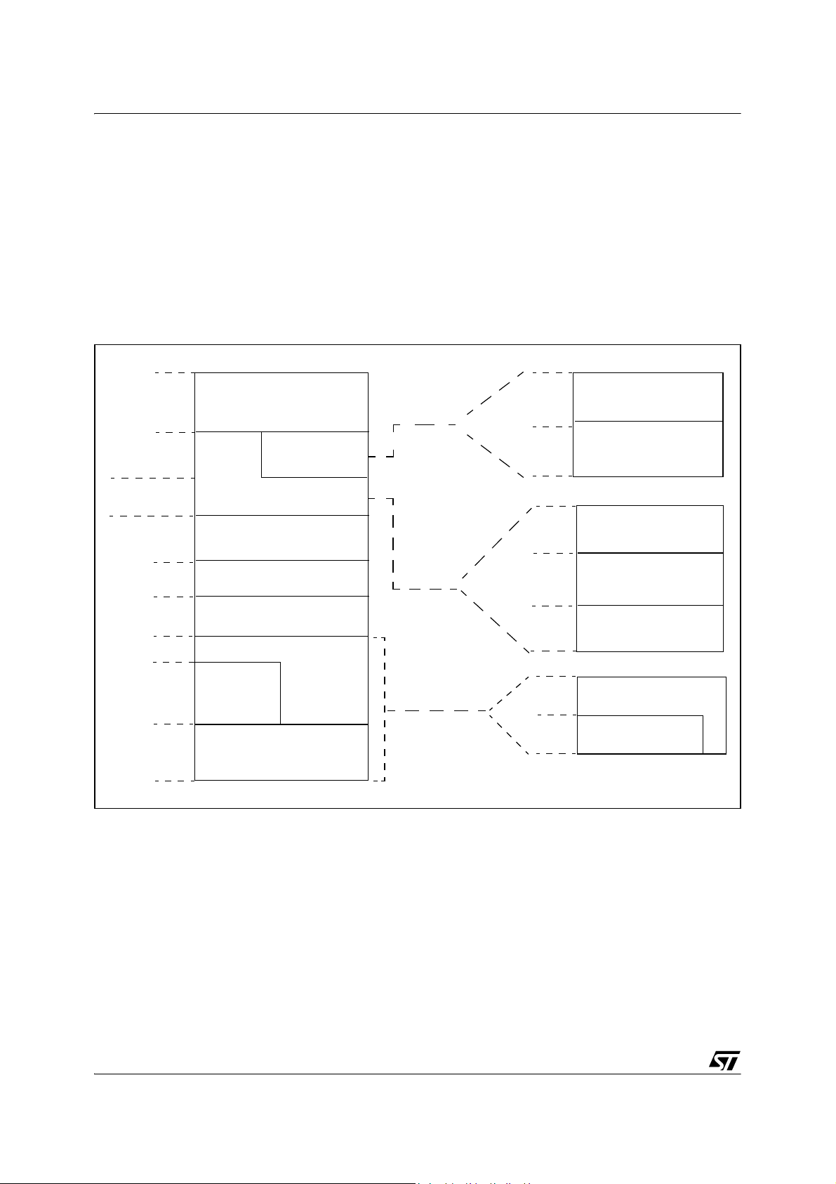
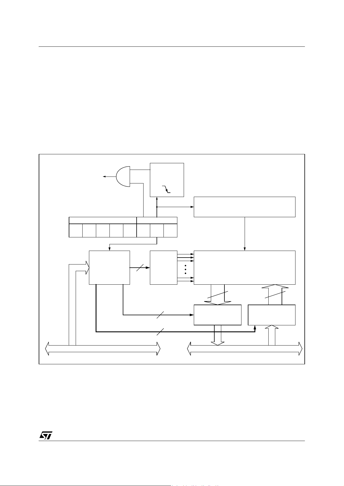
Figure 1. General Block Diagram
8-bit CORE
ALU
RESET
ISPSEL
V
DD
V
SS
CONTROL
LVD
-
-
-
Flash memory with byte-by-byte In-Situ Program
-
ming (ISP) capability.
Under software control, all devices can be placed
in Wait, Slow, Active Halt or Halt mode, reducing
power consumption when the application is in idle
or standby state.
The enhanced instruction set and addressing
modes of the ST7 offer both power and flexibility to
software developers, enabling the design of highly
efficient and compact application code. In addition
to standard 8-bit data management, all ST7 micro
controllers feature true bit manipulation, 8x8 unsigned multiplication and indirect addressing
modes.
For easy reference, all parametric data is located
Section 15 on page 108.
in
PROGRAM
MEMORY
(8 or 16 Kbytes)
RAM
(384 or 512 bytes)
OSC1
OSC2
PF7,6,4,2:0
(6-bit)
PE7:0
(6-bit for N versions)
(2-bit for J versions)
8/150
MULTI-OSC
+
CLOCK FILTER
MCC/RTC
PORT F
TIMER A
BEEP
PORT E
SCI
WATCHDOG
EEPROM
ADDRESS AND DATA BUS
(256 bytes)
PORT A
PORT B
PORT C
TIMER B
SPI
PORT D
8-bit ADC
PA7:0
(8-bit for N versions)
(5-bit for J versions)
PB7:0
(8-bit for N versions)
(5-bit for J versions)
PC7:0
(8-bit)
PD7:0
(8-bit for N versions)
(6-bit for J versions)
V
DDA
V
SSA
ST72334xx-Auto, ST72314xx-Auto, ST72124Jx-Auto
3 PIN DESCRIPTION
Figure 2. 64-Pin TQFP Package Pinout (N versions)
(HS) PE4
(HS) PE5
(HS) PE6
(HS) PE7
PB0
PB1
PB2
PB3
PB4
PB5
PB6
PB7
AIN0 / PD0
AIN1 / PD1
AIN2 / PD2
AIN3 / PD3
_2
DD
NCNCPE1 / RDI
64 63 62 61 60 59 58 57 56 55 54 53 52 51 50 49
1
V
PE0 / TDO
_2
SS
OSC1
OSC2
V
NCNCRESET
ISPSEL PA7 (HS)
PA6 (HS)
2
3
4
5
6
ei2
7
ei0
8
9
10
ei3
11
12
13
14
DD_3
V
ei1
SS_3
V
MCO / PF0
PF2
BEEP / PF1
NC
NC
15
16
17 18 19 20 21 22 23 24 29 30 31 3225 26 27 28
SSA
DDA
V
V
AIN4 / PD4
AIN5 / PD5
AIN6 / PD6
AIN7 / PD7
OCMP1_A / PF4
PA5 (HS)
46
45
44
43
ICAP1_A / (HS) PF6
PA4 (HS)
V
48
SS_1
V
47
DD_1
PA3
PA2
PA1
PA0
PC7 / SS
42
PC6 / SCK / ISPCLK
41
PC5 / MOSI
40
PC4 / MISO / ISPDATA
39
PC3 (HS) / ICAP1_B
38
PC2 (HS) / ICAP2_B
37
PC1 / OCMP1_B
36
PC0 / OCMP2_B
35
V
34
SS_0
V
33
DD_0
EXTCLK_A / (HS) PF7
(HS) 20mA high sink capability
associated external interrupt vector
ei
x
9/150
ST72334xx-Auto, ST72314xx-Auto, ST72124Jx-Auto
PIN DESCRIPTION (Cont’d)
Figure 3. 44-Pin TQFP Package Pinout (J versions)
PE1 / RDI
PB0
PB1
PB2
PB3
PB4
AIN0 / PD0
AIN1 / PD1
AIN2 / PD2
AIN3 / PD3
AIN4 / PD4
_2
DD
PE0 / TDO
V
44 43 42 41 40 39 38 37 36 35 34
1
_2
SS
V
RESET
ISPSEL PA7 (HS)
OSC1
OSC2
PA6 (HS)
2
3
ei2
4
ei0
5
ei3
6
7
8
9
DDA
V
ei1
19 20 21 22
SSA
V
PF2
MCO / PF0
BEEP / PF1
10
11
12 13 14 15 16 17 18
AIN5 / PD5
OCMP1_A / PF4
ICAP1_A / (HS) PF6
EXTCLK_A / (HS) PF7
PA5 (HS)
DD_0
V
PA4 (HS)
V
33
SS_1
V
32
DD_1
PA3
31
PC7 / SS
30
PC6 / SCK / ISPCLK
29
PC5 / MOSI
28
PC4 / MISO / ISPDATA
27
PC3 (HS) / ICAP1_B
26
PC2 (HS) / ICAP2_B
25
PC1 / OCMP1_B
24
PC0 / OCMP2_B
23
SS_0
V
(HS) 20mA high sink capability
eixassociated external interrupt vector
10/150
ST72334xx-Auto, ST72314xx-Auto, ST72124Jx-Auto
PIN DESCRIPTION (Cont’d)
For external pin connection guidelines, refer to Section 15 "ELECTRICAL CHARACTERISTICS" on page
108.
Legend / Abbreviations for Table 1:
Type: I = input, O = output, S = supply
Input level: A = Dedicated analog input
In/Output level: C = CMOS 0.3VDD/0.7VDD,
CT= CMOS 0.3VDD/0.7VDD with input trigger
Output level: HS = 20mA high sink (on N-buffer only)
Port and control configuration:
– Input: float = floating, wpu = weak pull-up, int = interrupt
– Output: OD = open drain
2)
, PP = push-pull
Refer to Section 11 "I/O PORTS" on page 40 for more details on the software configuration of the I/O
ports.
The RESET configuration of each pin is shown in bold. This configuration is valid as long as the device is
in reset state.
Table 1. Device Pin Description
1)
, ana = analog
Pin
No.
TQFP64
Pin Name
TQFP44
Level Port
Type
Input
Input Output
Output
float
Main
function
(after
int
wpu
ana
OD
PP
reset)
1 - PE4 (HS) I/O CTHS X X X X Port E4
2 - PE5 (HS) I/O CTHS X X X X Port E5
3 - PE6 (HS) I/O CTHS X X X X Port E6
4 - PE7 (HS) I/O CTHS X X X X Port E7
5 2 PB0 I/O C
6 3 PB1 I/O C
7 4 PB2 I/O C
8 5 PB3 I/O C
9 6 PB4 I/O C
10 - PB5 I/O C
11 - PB6 I/O C
12 - PB7 I/O C
13 7 PD0/AIN0 I/O C
14 8 PD1/AIN1 I/O C
15 9 PD2/AIN2 I/O C
16 10 PD3/AIN3 I/O C
17 11 PD4/AIN4 I/O C
18 12 PD5/AIN5 I/O C
19 - PD6/AIN6 I/O C
20 - PD7/AIN7 I/O C
21 13 V
22 14 V
23 - V
DDA
SSA
DD_3
S Analog Power Supply Voltage
S Analog Ground Voltage
S Digital Main Supply Voltage
X ei2 X X Port B0
T
X ei2 X X Port B1
T
X ei2 X X Port B2
T
X ei2 X X Port B3
T
X ei3 X X Port B4
T
X ei3 X X Port B5
T
X ei3 X X Port B6
T
X ei3 X X Port B7
T
X X X X X Port D0 ADC Analog Input 0
T
X X X X X Port D1 ADC Analog Input 1
T
X X X X X Port D2 ADC Analog Input 2
T
X X X X X Port D3 ADC Analog Input 3
T
X X X X X Port D4 ADC Analog Input 4
T
X X X X X Port D5 ADC Analog Input 5
T
X X X X X Port D6 ADC Analog Input 6
T
X X X X X Port D7 ADC Analog Input 7
T
Alternate function
11/150
ST72334xx-Auto, ST72314xx-Auto, ST72124Jx-Auto
Pin
No.
Pin Name
TQFP64
TQFP44
24 - V
SS_3
25 15 PF0/MCO I/O C
26 16 PF1/BEEP I/O C
27 17 PF2 I/O C
Level Port
Type
Input
Input Output
Output
float
int
wpu
ana
OD
function
PP
Main
(after
reset)
Alternate function
S Digital Ground Voltage
X ei1 X X Port F0 Main clock output (f
T
X ei1 X X Port F1 Beep signal output
T
X ei1 X X Port F2
T
OSC
/2)
28 - NC Not Connected
29 18 PF4/OCMP1_A I/O C
X X X X Port F4 Timer A Output Compare 1
T
30 - NC Not Connected
31 19 PF6 (HS)/ICAP1_A I/O CTHS X X X X Port F6 Timer A Input Capture 1
32 20 PF7 (HS)/EXTCLK_A I/O CTHS X X X X Port F7 Timer A External Clock Source
33 21 V
34 22 V
DD_0
SS_0
35 23 PC0/OCMP2_B I/O C
36 24 PC1/OCMP1_B I/O C
S Digital Main Supply Voltage
S Digital Ground Voltage
X X X X Port C0 Timer B Output Compare 2
T
X X X X Port C1 Timer B Output Compare 1
T
37 25 PC2 (HS)/ICAP2_B I/O CTHS X X X X Port C2 Timer B Input Capture 2
38 26 PC3 (HS)/ICAP1_B I/O CTHS X X X X Port C3 Timer B Input Capture 1
39 27 PC4/MISO I/O C
40 28 PC5/MOSI I/O C
41 29 PC6/SCK I/O C
42 30 PC7/SS I/O C
43 - PA0 I/O C
44 - PA1 I/O C
45 - PA2 I/O C
46 31 PA3 I/O C
47 32 V
48 33 V
DD_1
SS_1
S Digital Main Supply Voltage
S Digital Ground Voltage
X X X X Port C4 SPI Master In / Slave Out Data
T
X X X X Port C5 SPI Master Out / Slave In Data
T
X X X X Port C6 SPI Serial Clock
T
X X X X Port C7 SPI Slave Select (active low)
T
X ei0 X X Port A0
T
X ei0 X X Port A1
T
X ei0 X X Port A2
T
X ei0 X X Port A3
T
49 34 PA4 (HS) I/O CTHS X X X X Port A4
50 35 PA5 (HS) I/O CTHS X X X X Port A5
51 36 PA6 (HS) I/O CTHS X T Port A6
52 37 PA7 (HS) I/O CTHS X T Port A7
Must be tied low in user mode. In programming
53 38 ISPSEL I
mode when available, this pin acts as In-Situ
Programming mode selection.
54 39 RESET I/O C X X Top priority non maskable interrupt (active low)
55 - NC
56 - NC
57 40 V
SS_3
58 41 OSC2
59 42 OSC1
60 43 V
DD_3
S Digital Ground Voltage
3)
3)
O
I
S Digital Main Supply Voltage
Not Connected
Resonator oscillator inverter output or capacitor input for RC oscillator
External clock input or Resonator oscillator inverter input or resistor input for RC oscillator
12/150

ST72334xx-Auto, ST72314xx-Auto, ST72124Jx-Auto
Pin
No.
Pin Name
TQFP64
TQFP44
61 44 PE0/TDO I/O C
62 1 PE1/RDI I/O C
63 - NC
64 - NC
Level Port
Type
Input
T
T
Input Output
Output
float
X X X X Port E0 SCI Transmit Data Out
X X X X Port E1 SCI Receive Data In
Main
function
(after
int
wpu
ana
OD
reset)
PP
Not Connected
Alternate function
Notes:
1. In the interrupt input column, “eix” defines the associated external interrupt vector. If the weak pull-up
column (wpu) is merged with the interrupt column (int), then the I/O configuration is pull-up interrupt input,
else the configuration is floating interrupt input.
2. In the open drain output column, “T” defines a true open drain I/O (P-Buffer and protection diode to V
are not implemented). See Section 11 "I/O PORTS" on page 40 and Section 15.8 "I/O PORT PIN CHAR-
DD
ACTERISTICS" on page 129 for more details.
3. OSC1 and OSC2 pins connect a crystal or ceramic resonator, an external RC, or an external source to
the on-chip oscillator see
Section 3 "PIN DESCRIPTION" on page 9 and Section 15.5 "CLOCK AND TIM-
ING CHARACTERISTICS" on page 117 for more details.
13/150
ST72334xx-Auto, ST72314xx-Auto, ST72124Jx-Auto
4 REGISTER AND MEMORY MAP
As shown in the Figure 4, the MCU is capable of
addressing 64 Kbytes of memories and I/O registers.
The available memory locations consist of 128
bytes of register locations, 384 or 512 bytes of
RAM, up to 256 bytes of data EEPROM and 4 or
Kbytes of user program memory. The RAM
8
Figure 4. Memory Map
0000h
007Fh
0080h
01FFh
027Fh
0200h / 0280h
0BFFh
0C00h
0CFFh
0D00h
BFFFh
C000h
E000h
FFDFh
FFE0h
FFFFh
HW Registers
(see Table 2)
384 bytes RAM
512 bytes RAM
Reserved
256 bytes Data EEPROM
Reserved
16 Kbytes
8 Kbytes
Program
Memory
Interrupt and Reset Vectors
(see Table 6 on page 35)
Program
Memory
space includes up to 256 bytes for the stack from
0100h to 01FFh.
The highest address bytes contain the user reset
and interrupt vectors.
IMPORTANT: Memory locations marked as “Reserved” must never be accessed. Accessing a reserved area can have unpredictable effects on the
device.
0080h
00FFh
0100h
01FFh
0080h
00FFh
0100h
01FFh
0200h
027Fh
C000h
E000h
FFFFh
Short Addressing RAM
Zero page
(128 bytes)
Stack or
16-bit Addressing RAM
(256 bytes)
Short Addressing RAM
Zero page
(128 bytes)
Stack or
16-bit Addressing RAM
(256 bytes)
16-bit Addressing
RAM
16 Kbytes
8 Kbytes
14/150

REGISTER AND MEMORY MAP (Cont’d)
Table 2. Hardware Register Map
ST72334xx-Auto, ST72314xx-Auto, ST72124Jx-Auto
Address Block
0000h
0001h
Port A
0002h
Register
Label
PADR
PADDR
PAOR
Register Name
Port A Data Register
Port A Data Direction Register
Port A Option Register
0003h Reserved Area (1 byte)
0004h
0005h
0006h
Port C
PCDR
PCDDR
PCOR
Port C Data Register
Port C Data Direction Register
Port C Option Register
0007h Reserved Area (1 byte)
0008h
0009h
000Ah
Port B
PBDR
PBDDR
PBOR
Port B Data Register
Port B Data Direction Register
Port B Option Register
000Bh Reserved Area (1 byte)
000Ch
000Dh
000Eh
Port E
PEDR
PEDDR
PEOR
Port E Data Register
Port E Data Direction Register
Port E Option Register
000Fh Reserved Area (1 byte)
0010h
0011h
0012h
Port D
PDDR
PDDDR
PDOR
Port D Data Register
Port D Data Direction Register
Port D Option Register
Reset
Status
1)
00h
00h
00h
1)
00h
00h
00h
1)
00h
00h
00h
1)
00h
00h
00h
1)
00h
00h
00h
Remarks
R/W
R/W
2)
R/W
R/W
R/W
R/W
R/W
R/W
2)
R/W
R/W
R/W
2)
R/W
R/W
R/W
2)
R/W
0013h Reserved Area (1 byte)
0014h
0015h
0016h
Port F
PFDR
PFDDR
PFOR
Port F Data Register
Port F Data Direction Register
Port F Option Register
00h
00h
00h
1)
R/W
R/W
R/W
0017h
to
Reserved Area (9 bytes)
001Fh
0020h MISCR1 Miscellaneous Register 1 00h R/W
0021h
0022h
0023h
SPI
SPIDR
SPICR
SPISR
SPI Data I/O Register
SPI Control Register
SPI Status Register
xxh
0xh
00h
R/W
R/W
Read Only
0024h
to
Reserved Area (5 bytes)
0028h
0029h MCC MCCSR Main Clock Control / Status Register 01h R/W
15/150

ST72334xx-Auto, ST72314xx-Auto, ST72124Jx-Auto
Address Block
Register
Label
Register Name
Reset
Status
002Ah WATCHDOG WDGCR Watchdog Control Register 7Fh R/W
002Bh CRSR Clock, Reset, Supply Control / Status Register 000x 000x R/W
002Ch Data-EEPROM EECSR Data-EEPROM Control/Status Register 00h R/W
002Dh
0030h
0031h
0032h
0033h
0034h
0035h
0036h
0037h
0038h
0039h
003Ah
003Bh
003Ch
003Dh
003Eh
003Fh
TIMER A
TACR2
TACR1
TASR
TAIC1HR
TAIC1LR
TAOC1HR
TAOC1LR
TACHR
TACLR
TAACHR
TAACLR
TAIC2HR
TAIC2LR
TAOC2HR
TAOC2LR
Timer A Control Register 2
Timer A Control Register 1
Timer A Status Register
Timer A Input Capture 1 High Register
Timer A Input Capture 1 Low Register
Timer A Output Compare 1 High Register
Timer A Output Compare 1 Low Register
Timer A Counter High Register
Timer A Counter Low Register
Timer A Alternate Counter High Register
Timer A Alternate Counter Low Register
Timer A Input Capture 2 High Register
Timer A Input Capture 2 Low Register
Timer A Output Compare 2 High Register
Timer A Output Compare 2 Low Register
Reserved Area (4 bytes)
00h
00h
xxh
xxh
xxh
80h
00h
FFh
FCh
FFh
FCh
xxh
xxh
80h
00h
Remarks
R/W
R/W
Read Only
Read Only
Read Only
R/W
R/W
Read Only
Read Only
Read Only
Read Only
Read Only 3)
Read Only
R/W
R/W
3)
3)
3)
0040h MISCR2 Miscellaneous Register 2 00h R/W
0041h
0042h
0043h
0044h
0045h
0046h
0047h
0048h
0049h
004Ah
004Bh
004Ch
004Dh
004Eh
004Fh
0050h
0051h
0052h
0053h
0054h
0055h
0056h
0057h
0058h
006Fh
TIMER B
SCI
TBCR2
TBCR1
TBSR
TBIC1HR
TBIC1LR
TBOC1HR
TBOC1LR
TBCHR
TBCLR
TBACHR
TBACLR
TBIC2HR
TBIC2LR
TBOC2HR
TBOC2LR
SCISR
SCIDR
SCIBRR
SCICR1
SCICR2
SCIERPR
SCIETPR
Timer B Control Register 2
Timer B Control Register 1
Timer B Status Register
Timer B Input Capture 1 High Register
Timer B Input Capture 1 Low Register
Timer B Output Compare 1 High Register
Timer B Output Compare 1 Low Register
Timer B Counter High Register
Timer B Counter Low Register
Timer B Alternate Counter High Register
Timer B Alternate Counter Low Register
Timer B Input Capture 2 High Register
Timer B Input Capture 2 Low Register
Timer B Output Compare 2 High Register
Timer B Output Compare 2 Low Register
SCI Status Register
SCI Data Register
SCI Baud Rate Register
SCI Control Register 1
SCI Control Register 2
SCI Extended Receive Prescaler Register
Reserved area
SCI Extended Transmit Prescaler Register
Reserved Area (24 bytes)
00h
00h
xxh
xxh
xxh
80h
00h
FFh
FCh
FFh
FCh
xxh
xxh
80h
00h
C0h
xxh
00xx xxxx
xxh
00h
00h
---
00h
R/W
R/W
Read Only
Read Only
Read Only
R/W
R/W
Read Only
Read Only
Read Only
Read Only
Read Only
Read Only
R/W
R/W
Read Only
R/W
R/W
R/W
R/W
R/W
R/W
16/150

ST72334xx-Auto, ST72314xx-Auto, ST72124Jx-Auto
Address Block
0070h
0071h
0072h
to
007Fh
ADC
Register
Label
ADCDR
ADCCSR
Register Name
Data Register
Control/Status Register
Reserved Area (14 bytes)
Reset
Status
xxh
00h
Remarks
Read Only
R/W
Legend: x=undefined, R/W=read/write
Notes:
1. The contents of the I/O port DR registers are readable only in output configuration. In input configuration, the values
of the I/O pins are returned instead of the DR register contents.
2. The bits corresponding to unavailable pins are forced to 1 by hardware, affecting accordingly the reset status value.
These bits must always keep their reset value.
3. External pin not available.
17/150
ST72334xx-Auto, ST72314xx-Auto, ST72124Jx-Auto
5 FLASH PROGRAM MEMORY
5.1 INTRODUCTION
Flash devices have a single voltage non-volatile
Flash memory that may be programmed in-situ (or
plugged in a programming tool) on a byte-by-byte
basis.
5.2 MAIN FEATURES
■ Remote In-Situ Programming (ISP) mode
■ Up to 16 bytes programmed in the same cycle
■ MTP memory (Multiple Time Programmable)
■ Readout memory protection against piracy
5.3 STRUCTURAL ORGANIZATION
The Flash program memory is organized in a single 8-bit wide memory block which can be used for
storing both code and data constants.
The Flash program memory is mapped in the upper part of the ST7 addressing space and includes
the reset and interrupt user vector area.
5.4 IN-SITU PROGRAMMING (ISP) MODE
The Flash program memory can be programmed
using Remote ISP mode. This ISP mode allows
the contents of the ST7 program memory to be up
dated using a standard ST7 programming tools after the device is mounted on the application board.
This feature can be implemented with a minimum
number of added components and board area im
pact.
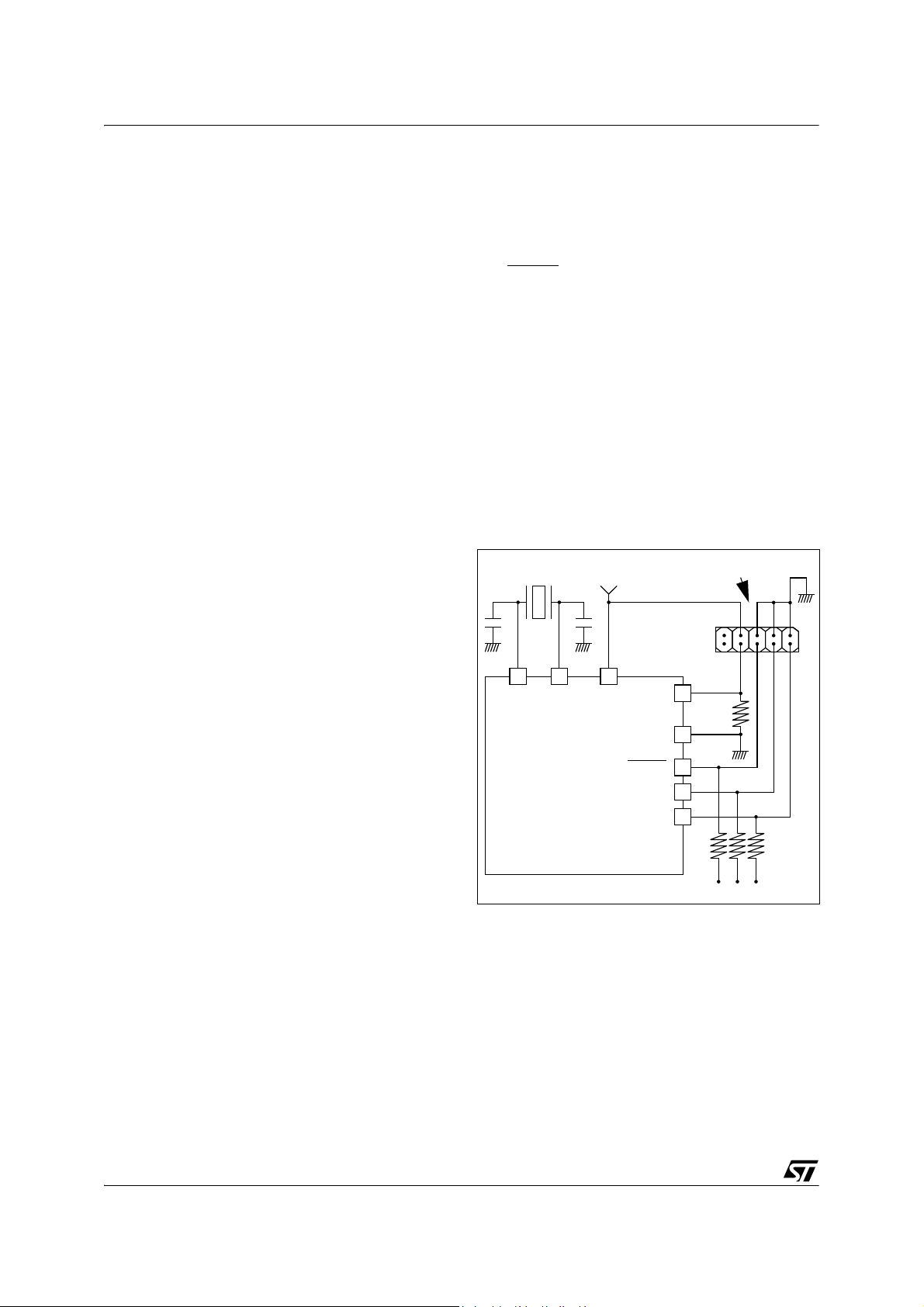
An example Remote ISP hardware interface to the
standard ST7 programming tool is described be
low. For more details on ISP programming, refer to
the ST7 Programming Specification.
Remote ISP Overview
The Remote ISP mode is initiated by a specific sequence on the dedicated ISPSEL pin.
The Remote ISP is performed in three steps:
– Selection of the RAM execution mode
– Download of Remote ISP code in RAM
– Execution of Remote ISP code in RAM to pro-
gram the user program into the Flash
Remote ISP hardware configuration
In Remote ISP mode, the ST7 has to be supplied
with power (V
and VSS) and a clock signal (os-
DD
cillator and application crystal circuit for example).
This mode needs five signals (plus the VDD signal
if necessary) to be connected to the programming
tool. This signals are:
– RESET: device reset
–VSS: device ground power supply
– ISPCLK: ISP output serial clock pin
– ISPDATA: ISP input serial data pin
– ISPSEL: Remote ISP mode selection. This pin
must be connected to V
board through a pull-down resistor.
on the application
SS
If any of these pins are used for other purposes on
the application, a serial resistor has to be imple
mented to avoid a conflict if the other device forces
the signal level.
Figure 5 shows a typical hardware interface to a
standard ST7 programming tool. For more details
on the pin locations, refer to the device pinout de
scription.
Figure 5. Typical Remote ISP Interface
HE10 CONNECTOR TYPE
XTAL
C
L0
C
L1
-
OSC1
OSC2
TO PROGRAMMING TOOL
ISPSEL
DD
V
V
10KΩ
SS
-
RESET
-
ST7
ISPCLK
ISPDATA
APPLICATION
5.5 MEMORY READOUT PROTECTION
The readout protection is enabled through an option bit.
For Flash devices, when this option is selected,
the program and data stored in the Flash memory
are protected against readout piracy (including a
re-write protection). When this protection option is
removed the entire Flash program memory is first
automatically erased. However, the EEPROM
data memory (when available) can be protected
only with ROM devices.
-
-
1
47KΩ
18/150
6 DATA EEPROM
ST72334xx-Auto, ST72314xx-Auto, ST72124Jx-Auto
6.1 INTRODUCTION
The Electrically Erasable Programmable Read
Only Memory can be used as a non-volatile backup for storing data. Using the EEPROM requires a
basic access protocol described in this chapter.
Figure 6. EEPROM Block Diagram
FALLING
EEPROM INTERRUPT
EECSR
IE LAT00 0 0 0 PGM
EDGE
DETECTOR
EEPROMRESERVED
6.2 MAIN FEATURES
■ Up to 16 bytes programmed in the same cycle
■ EEPROM mono-voltage (charge pump)
■ Chained erase and programming cycles
■ Internal control of the global programming cycle
duration
■ End of programming cycle interrupt flag
■ Wait mode management
HIGH VOLTAGE
PUMP
ADDRESS
DECODER
ADDRESS BUS
4
ROW
DECODER
4
4
MEMORY MATRIX
(1 ROW = 16 x 8 BITS)
DATA
MULTIPLEXER
EEPROM
128128
16 x 8 BITS
DATA LATCHES
DATA BUS
19/150
ST72334xx-Auto, ST72314xx-Auto, ST72124Jx-Auto
DATA EEPROM (Cont’d)
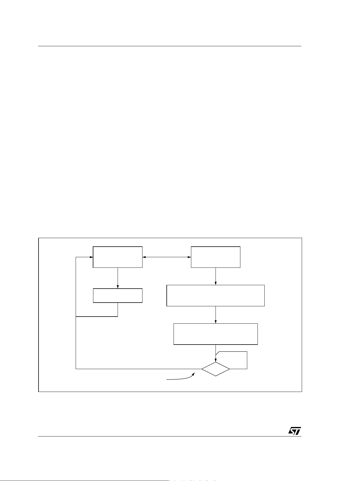
6.3 MEMORY ACCESS
The Data EEPROM memory read/write access
modes are controlled by the LAT bit of the EEP
ROM Control/Status register (EECSR). The flowchart in Figure 7 describes these different memory
access modes.
Read Operation (LAT=0)
The EEPROM can be read as a normal ROM location when the LAT bit of the EECSR register is
cleared. In a read cycle, the byte to be accessed is
put on the data bus in less than 1 CPU clock cycle.
This means that reading data from EEPROM
takes the same time as reading data from
EPROM, but this memory cannot be used to exe
cute machine code.
Write Operation (LAT=1)
To access the write mode, the LAT bit has to be
set by software (the PGM bit remains cleared).
When a write access to the EEPROM area occurs,
the value is latched inside the 16 data latches ac
cording to its address.
Figure 7. Data EEPROM Programming Flowchart
When PGM bit is set by the software, all the previous bytes written in the data latches (up to 16) are
programmed in the EEPROM cells. The effective
high address (row) is determined by the last EEP
ROM write sequence. To avoid wrong programming, the user must take care that all the bytes
written between two programming sequences
have the same high address: only the four Least
Significant Bits of the address can change.
At the end of the programming cycle, the PGM and
LAT bits are cleared simultaneously, and an inter
rupt is generated if the IE bit is set. The Data EEPROM interrupt request is cleared by hardware
when the Data EEPROM interrupt vector is
fetched.
Note: Care should be taken during the programming cycle. Writing to the same memory location
will over-program the memory (logical AND be
tween the two write access data result) because
the data latches are only cleared at the end of the
programming cycle and by the falling edge of LAT
bit.
It is not possible to read the latched data.
This note is illustrated by the Figure 8.
READ MODE
LAT=0
PGM=0
READ BYTES
IN EEPROM AREA
INTERRUPT GENERATION
IF IE=1 0 1
CLEARED BY HARDWARE
WRITE MODE
LAT=1
PGM=0
WRITE UP TO 16 BYTES
IN EEPROM AREA
(with the same 11 MSB of the address)
START PROGRAMMING CYCLE
LAT=1
PGM=1 (set by software)
LAT
20/150
DATA EEPROM (Cont’d)
ST72334xx-Auto, ST72314xx-Auto, ST72124Jx-Auto
6.4 POWER SAVING MODES
Wait mode
The Data EEPROM can enter Wait mode on execution of the WFI instruction of the microcontroller.
The Data EEPROM will immediately enter this
mode if there is no programming in progress, oth
erwise the Data EEPROM will finish the cycle and
then enter Wait mode.
Halt mode
The Data EEPROM immediately enters Halt mode
if the microcontroller executes the HALT instruc
tion. Therefore the EEPROM will stop the function
in progress, and data may be corrupted.
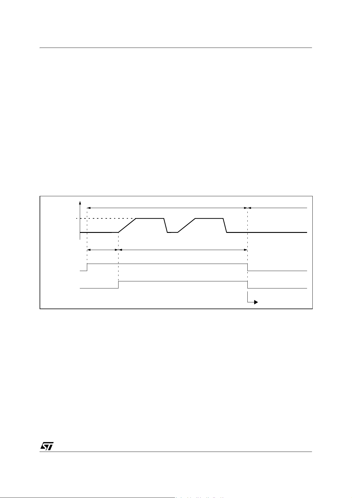
Figure 8. Data EEPROM Programming Cycle
READ OPERATION NOT POSSIBLE
INTERNAL
PROGRAMMING
VOLTAGE
ERASE CYCLE WRITE CYCLE
WRITE OF
DATA LATCHES
6.5 ACCESS ERROR HANDLING
If a read access occurs while LAT=1, then the data
bus will not be driven.
If a write access occurs while LAT=0, then the
data on the bus will not be latched.
If a programming cycle is interrupted (by software/
RESET action), the memory data will not be guar
anteed.
READ OPERATION POSSIBLE
t
PROG
-
EEPROM INTERRUPT
LAT
PGM
21/150

ST72334xx-Auto, ST72314xx-Auto, ST72124Jx-Auto
DATA EEPROM (Cont’d)
6.6 REGISTER DESCRIPTION
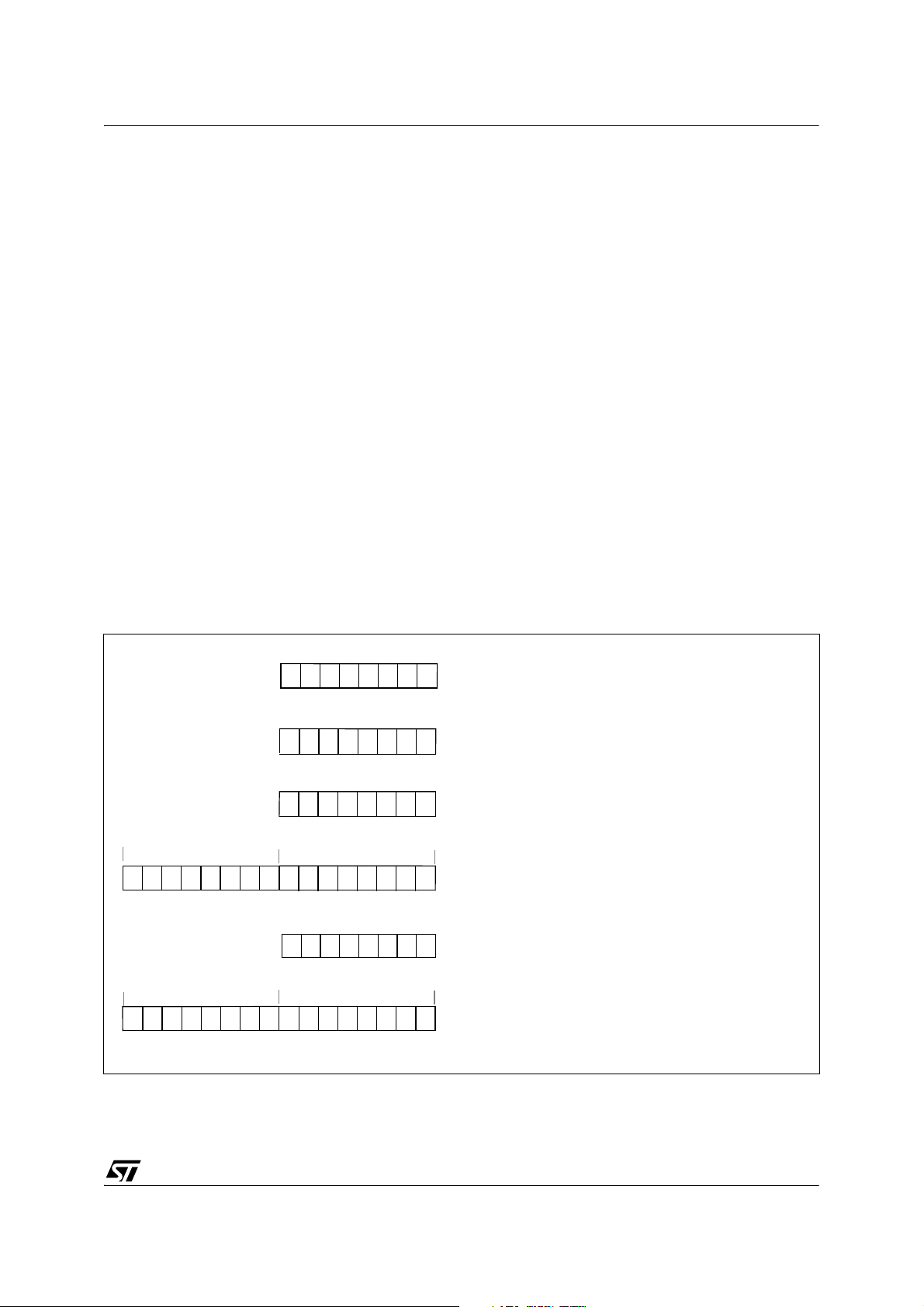
Bit 1 = LAT Latch Access Transfer
This bit is set by software. It is cleared by hard-
CONTROL/STATUS REGISTER (CSR)
Read / Write
Reset Value: 0000 0000 (00h)
7 0
ware at the end of the programming cycle. It can
only be cleared by software if PGM bit is cleared.
0: Read mode
1: Write mode
Bit 0 = PGM Programming control and status
0 0 0 0 0 IE LAT PGM
This bit is set by software to begin the programming
cycle. At the end of the programming cycle, this bit
is cleared by hardware and an interrupt is generated
Bit 7:3 = Reserved, forced by hardware to 0.
if the ITE bit is set.
0: Programming finished or not yet started
1: Programming cycle is in progress
Bit 2 = IE Interrupt enable
This bit is set and cleared by software. It enables the
Data EEPROM interrupt capability when the PGM
bit is cleared by hardware. The interrupt request is
Note: if the PGM bit is cleared during the programming cycle, the memory data is not guaranteed
automatically cleared when the software enters the
interrupt routine.
0: Interrupt disabled
1: Interrupt enabled
Table 3. Data EEPROM Register Map and Reset Values
Address
(Hex.)
002Ch
Register
Label
EECSR
Reset Value 0 0 0 0 0
7 6 5 4 3 2 1 0
IE
0
RWM
0
PGM
0
6.7 READOUT PROTECTION OPTION
The Data EEPROM can be optionally readout protected in ST72334 ROM devices (see option list on
22/150
page 145). ST72C334 Flash devices do not have
this protection option.
7 CENTRAL PROCESSING UNIT
ST72334xx-Auto, ST72314xx-Auto, ST72124Jx-Auto
7.1 INTRODUCTION
This CPU has a full 8-bit architecture and contains
six internal registers allowing efficient 8-bit data
manipulation.
7.2 MAIN FEATURES
■ 63 basic instructions
■ Fast 8-bit by 8-bit multiply
■ 17 main addressing modes
■ Two 8-bit index registers
■ 16-bit stack pointer
■ Low power modes
■ Maskable hardware interrupts
■ Non-maskable software interrupt
7.3 CPU REGISTERS
The six CPU registers shown in Figure 9 are not
present in the memory mapping and are accessed
by specific instructions.
Figure 9. CPU Registers
70
RESET VALUE = XXh
70
RESET VALUE = XXh
70
RESET VALUE = XXh
Accumulator (A)
The Accumulator is an 8-bit general purpose register used to hold operands and the results of the
arithmetic and logic calculations and to manipulate
data.
Index Registers (X and Y)
In indexed addressing modes, these 8-bit registers
are used to create either effective addresses or
temporary storage areas for data manipulation.
(The Cross-Assembler generates a precede in
struction (PRE) to indicate that the following instruction refers to the Y register.)
The Y register is not affected by the interrupt automatic procedures (not pushed to and popped from
the stack).
Program Counter (PC)
The program counter is a 16-bit register containing
the address of the next instruction to be executed
by the CPU. It is made of two 8-bit registers PCL
(Program Counter Low which is the LSB) and PCH
(Program Counter High which is the MSB).
ACCUMULATOR
X INDEX REGISTER
Y INDEX REGISTER
-
15 8
RESET VALUE = RESET VECTOR @ FFFEh-FFFFh
15
RESET VALUE = STACK HIGHER ADDRESS
PCH
RESET VALUE =
7
70
1C11HI NZ
1X11X1XX
70
8
PCL
0
PROGRAM COUNTER
CONDITION CODE REGISTER
STACK POINTER
X = Undefined Value
23/150

ST72334xx-Auto, ST72314xx-Auto, ST72124Jx-Auto
CPU REGISTERS (Cont’d)
CONDITION CODE REGISTER (CC)
Read/Write
Reset Value: 111x1xxx
7 0
1 1 1 H I N Z C
The 8-bit Condition Code register contains the interrupt mask and four flags representative of the
result of the instruction just executed. This register
can also be handled by the PUSH and POP in
structions.
These bits can be individually tested and/or controlled by specific instructions.
Bit 4 = H Half carry
This bit is set by hardware when a carry occurs be-
tween bits 3 and 4 of the ALU during an ADD or
ADC instruction. It is reset by hardware during the
same instructions.
0: No half carry has occurred.
1: A half carry has occurred.
This bit is tested using the JRH or JRNH instruction. The H bit is useful in BCD arithmetic subroutines.
Bit 3 = I Interrupt mask
This bit is set by hardware when entering in interrupt or by software to disable all interrupts except
the TRAP software interrupt. This bit is cleared by
software.
0: Interrupts are enabled.
1: Interrupts are disabled.
This bit is controlled by the RIM, SIM and IRET instructions and is tested by the JRM and JRNM instructions.
Note: Interrupts requested while I is set are
latched and can be processed when I is cleared.
By default an interrupt routine is not interruptible
because the I bit is set by hardware at the start of
the routine and reset by the IRET instruction at the
end of the routine. If the I bit is cleared by software
in the interrupt routine, pending interrupts are
serviced regardless of the priority level of the cur
rent interrupt routine.
Bit 2 = N Negative
This bit is set and cleared by hardware. It is repre-
sentative of the result sign of the last arithmetic,
logical or data manipulation. It is a copy of the 7
bit of the result.
0: The result of the last operation is positive or null.
1: The result of the last operation is negative
(that is, the most significant bit is a logic 1).
This bit is accessed by the JRMI and JRPL instructions.
-
Bit 1 = Z Zero
This bit is set and cleared by hardware. This bit indicates that the result of the last arithmetic, logical
or data manipulation is zero.
0: The result of the last operation is different from
zero.
1: The result of the last operation is zero.
This bit is accessed by the JREQ and JRNE test
instructions.
Bit 0 = C Carry/borrow
This bit is set and cleared by hardware and soft-
ware. It indicates an overflow or an underflow has
occurred during the last arithmetic operation.
0: No overflow or underflow has occurred.
1: An overflow or underflow has occurred.
This bit is driven by the SCF and RCF instructions
and tested by the JRC and JRNC instructions. It is
also affected by the “bit test and branch”, shift and
rotate instructions.
-
th
24/150
ST72334xx-Auto, ST72314xx-Auto, ST72124Jx-Auto
CENTRAL PROCESSING UNIT (Cont’d)
Stack Pointer (SP)
Read/Write
Reset Value: 01 FFh
15 8
0 0 0 0 0 0 0 1
7 0
SP7 SP6 SP5 SP4 SP3 SP2 SP1 SP0
The Stack Pointer is a 16-bit register which is always pointing to the next free location in the stack.
It is then decremented after data has been pushed
onto the stack and incremented before data is
popped from the stack (see
Since the stack is 256 bytes deep, the 8th most
significant bits are forced by hardware. Following
an MCU Reset, or after a Reset Stack Pointer in
struction (RSP), the Stack Pointer contains its reset value (the SP7 to SP0 bits are set) which is the
stack higher address.
Figure 10).
-
The least significant byte of the Stack Pointer
(called S) can be directly accessed by a LD in
-
struction.
Note: When the lower limit is exceeded, the Stack
Pointer wraps around to the stack upper limit, with
out indicating the stack overflow. The previously
stored information is then overwritten and there
fore lost. The stack also wraps in case of an underflow.
The stack is used to save the return address during a subroutine call and the CPU context during
an interrupt. The user may also directly manipulate
the stack by means of the PUSH and POP instruc
tions. In the case of an interrupt, the PCL is stored
at the first location pointed to by the SP. Then the
other registers are stored in the next locations as
shown in
Figure 10.
– When an interrupt is received, the SP is decre-
mented and the context is pushed on the stack.
– On return from interrupt, the SP is incremented
and the context is popped from the stack.
A subroutine call occupies two locations and an interrupt five locations in the stack area.
Figure 10. Stack Manipulation Example
@ 0100h
SP
@ 01FFh
CALL
Subroutine
SP
PCH
PCL
Stack Higher Address = 01FFh
Stack Lower Address =
Interrupt
Event
SP
CC
A
X
PCH
PCL
PCH
PCL
0100h
PUSH Y POP Y IRET
SP
Y
CC
A
X
PCH
PCL
PCH
PCL
CC
A
X
PCH
PCL
PCH
PCL
SP
PCH
PCL
RET
or RSP
SP
25/150
ST72334xx-Auto, ST72314xx-Auto, ST72124Jx-Auto
8 SUPPLY, RESET AND CLOCK MANAGEMENT
The ST72334J/N-Auto, ST72314J/N-Auto and
ST72124J-Auto microcontrollers include a range
of utility features for securing the application in crit
ical situations (for example, in case of a power
brown-out), and reducing the number of external
components. An overview is shown in
Figure 11.
See Section 15 "ELECTRICAL CHARACTERIS-
TICS" on page 108 for more details.
Main Features
■ Supply Manager with main supply low voltage
detection (LVD)
■ Reset Sequence Manager (RSM)
Figure 11. Clock, Reset and Supply Block Diagram
CLOCK SECURITY SYSTEM
(CSS)
OSC2
OSC1
MULTI-
OSCILLATOR
(MO)
CLOCK
FILTER
■ Multi-Oscillator (MO)
– 4 Crystal/Ceramic resonator oscillators
– 1 External RC oscillator
– 1 Internal RC oscillator
■ Clock Security System (CSS)
– Clock Filter
– Backup Safe Oscillator
SAFE
OSC
f
OSC
TO
MAIN CLOCK
CONTROLLER
RESET
V
DD
V
SS
RESET SEQUENCE
MANAGER
(RSM)
LOW VOLTAGE
DETECTOR
(LVD)
CRSR
FROM
WATCHDOG
PERIPHERAL
LVD
IE D00 0 0 RF RF
CSS INTERRUPT
CSS WDG
26/150
8.1 LOW VOLTAGE DETECTOR (LVD)
ST72334xx-Auto, ST72314xx-Auto, ST72124Jx-Auto
To allow the integration of power management
features in the application, the Low Voltage Detec
tor function (LVD) generates a static reset when
the V
supply voltage is below a V
DD
reference
IT-
value. This means that it secures the power-up as
well as the power-down keeping the ST7 in reset.
The V
than the V
to avoid a parasitic reset when the MCU starts run
reference value for a voltage drop is lower
IT-
reference value for power-on in order
IT+
ning and sinks current on the supply (hysteresis).
The LVD Reset circuitry generates a reset when
is below:
V
DD
–V
when VDD is rising
IT+
–V
when VDD is falling
IT-
The LVD function is illustrated in the Figure 12.
Provided the minimum VDD value (guaranteed for
the oscillator frequency) is above V
, the MCU
IT-
can only be in two modes:
– under full software control
– in static safe reset
Figure 12. Low Voltage Detector vs Reset
V
DD
In these conditions, secure operation is always ensured for the application without the need for external reset hardware.
During a Low Voltage Detector Reset, the RESET
pin is held low, thus permitting the MCU to reset
other devices.
Notes:
1. The LVD allows the device to be used without
any external RESET circuitry.
2. Three different reference levels are selectable
through the option byte according to the applica
tion requirement.
LVD application note
Application software can detect a reset caused by
the LVD by reading the LVDRF bit in the CRSR
register.
This bit is set by hardware when a LVD reset is
generated and cleared by software (writing zero).
-
V
IT+
V
IT-
RESET
V
hyst
27/150
ST72334xx-Auto, ST72314xx-Auto, ST72124Jx-Auto
8.2 RESET SEQUENCE MANAGER (RSM)
8.2.1 Introduction
The reset sequence manager includes three RESET sources as shown in Figure 14:
■ External RESET source pulse
■ Internal LVD RESET (Low Voltage Detection)
■ Internal WATCHDOG RESET
These sources act on the RESET pin and it is always kept low during the delay phase.
The RESET service routine vector is fixed at addresses FFFEh-FFFFh in the ST7 memory map.
The basic RESET sequence consists of three
phases as shown in
■ Delay depending on the RESET source
■ 4096 CPU clock cycle delay
■ RESET vector fetch
Figure 13:
Figure 14. Reset Block Diagram
V
DD
f
CPU
The 4096 CPU clock cycle delay allows the oscillator to stabilise and ensures that recovery has
taken place from the Reset state.
The RESET vector fetch phase duration is 2 clock
cycles.
Figure 13. RESET Sequence Phases
RESET
DELAY
INTERNAL RESET
4096 CLOCK CYCLES
FETCH
VECTOR
INTERNAL
RESET
RESET
R
ON
COUNTER
WATCHDOG RESET
LVD RESET
28/150
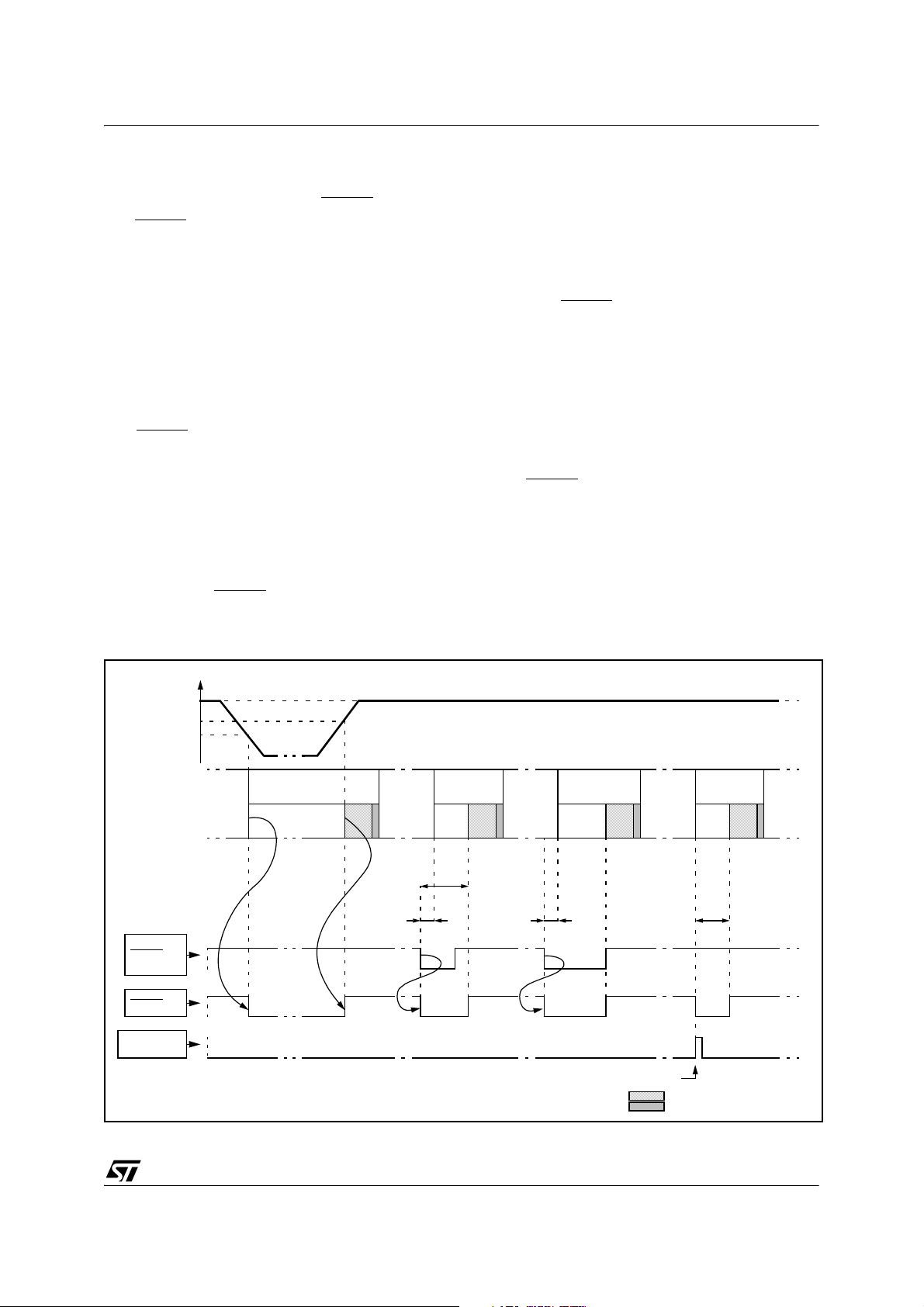
RESET SEQUENCE MANAGER (Cont’d)
ST72334xx-Auto, ST72314xx-Auto, ST72124Jx-Auto
8.2.2 Asynchronous External RESET Pin
The RESET pin is both an input and an open-drain
output with integrated R
This pull-up has no fixed value but varies in ac
weak pull-up resistor.
ON
cordance with the input voltage. It can be pulled
low by external circuitry to reset the device. See
ELECTRICAL CHARACTERISTICS section for
more details.
A RESET signal originating from an external
source must have a duration of at least t
h(RSTL)in
order to be recognized. This detection is asynchro
in
nous and therefore the MCU can enter reset state
even in Halt mode.
The RESET pin is an asynchronous signal which
plays a major role in EMS performance. In a noisy
environment, it is recommended to follow the
guidelines mentioned in the
ELECTRICAL CHAR-
ACTERISTICS section.
Two RESET sequences can be associated with
this RESET source: short or long external reset
pulse (see
Figure 15).
Starting from the external RESET pulse recognition, the device RESET pin acts as an output that
is pulled low during at least t
w(RSTL)out
.
Figure 15. RESET Sequences
8.2.3 Internal Low Voltage Detection RESET
Two different RESET sequences caused by the internal LVD circuitry can be distinguished:
■ Power-On RESET
■ Voltage Drop RESET
The device RESET pin acts as an output that is
pulled low when V
V
DD<VIT-
(falling edge) as shown in Figure 15.
DD<VIT+
The LVD filters spikes on V
(rising edge) or
larger than t
DD
g(VDD)
to
avoid parasitic resets.
8.2.4 Internal Watchdog RESET
The RESET sequence generated by an internal
Watchdog counter overflow is shown in
Figure 15.
Starting from the Watchdog counter underflow, the
device
low during at least t
RESET pin acts as an output that is pulled
w(RSTL)out
.
V
V
EXTERNAL
RESET
SOURCE
RESET PIN
WATCHDOG
RESET
IT+
IT-
V
DD
RUN
LVD
RESET
DELAY
RUN
t
w(RSTL)out
t
h(RSTL)in
SHORT EXT.
RESET
DELAY
LONG EXT.
RESET
RUN RUN
DELAY
t
h(RSTL)in
WATCHDOG UNDERFLOW
WATCHDOG
RESET
RUN
DELAY
t
w(RSTL)out
INTERNAL RESET (4096 T
FETCH VECTOR
CPU
)
29/150
ST72334xx-Auto, ST72314xx-Auto, ST72124Jx-Auto
8.3 MULTI-OSCILLATOR (MO)
The main clock of the ST7 can be generated by
four different source types coming from the multioscillator block:
■ an external source
■ 4 crystal or ceramic resonator oscillators
■ an external RC oscillator
■ an internal high frequency RC oscillator
Each oscillator is optimized for a given frequency
range in terms of consumption and is selectable
through the option byte. The associated hardware
configuration are shown in
Table 4. Refer to the
ELECTRICAL CHARACTERISTICS section for
more details.
External Clock Source
In this external clock mode, a clock signal (square,
sinus or triangle) with ~50% duty cycle has to drive
the OSC1 pin while the OSC2 pin is tied to ground.
Crystal/Ceramic Oscillators
This family of oscillators has the advantage of producing a very accurate rate on the main clock of
the ST7. The selection within a list of four oscilla
tors with different frequency ranges has to be done
by option byte in order to reduce consumption. In
this mode of the multi-oscillator, the resonator and
the load capacitors have to be placed as close as
possible to the oscillator pins in order to minimize
output distortion and start-up stabilization time.
The loading capacitance values must be adjusted
according to the selected oscillator.
These oscillators are not stopped during the RESET phase to avoid losing time in the oscillator
start-up phase.
the drawback of a lower frequency accuracy. Its
frequency is in the range of several MHz. This op
tion should not be used in applications that require
accurate timing.
In this mode, the two oscillator pins have to be tied
to ground.
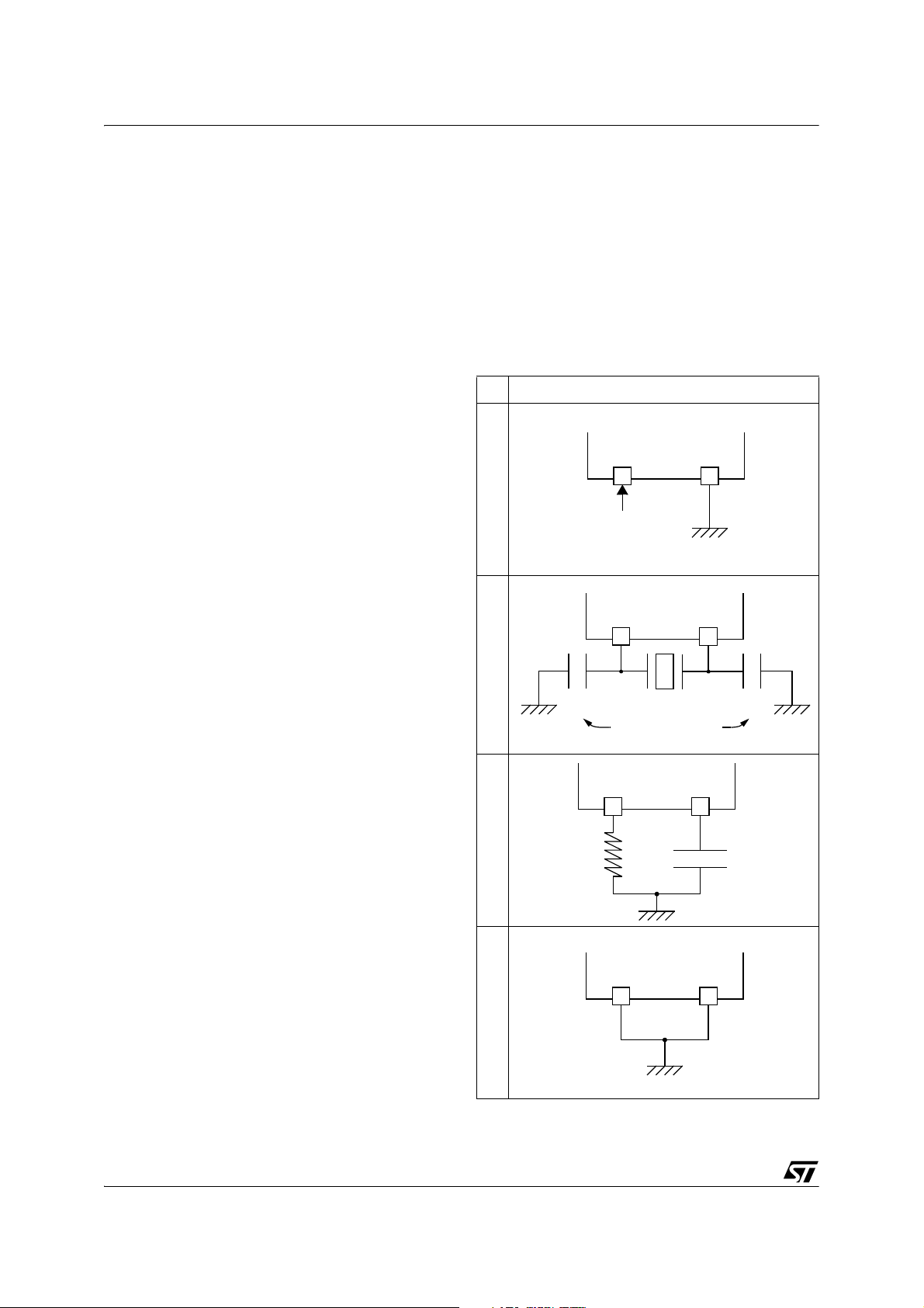
Table 4. ST7 Clock Sources
Hardware Configuration
ST7
OSC1 OSC2
External ClockCrystal/Ceramic ResonatorsExternal RC OscillatorInternal RC Oscillator
EXTERNAL
SOURCE
OSC1 OSC2
C
L1
OSC1 OSC2
LOAD
CAPACITORS
ST7
ST7
C
L2
-
External RC Oscillator
This oscillator allows a low cost solution for the
main clock of the ST7 using only an external resis
tor and an external capacitor. The frequency of the
external RC oscillator (in the range of some MHz)
is fixed by the resistor and the capacitor values.
Consequently in this MO mode, the accuracy of
the clock is dependent on V
, TA, process varia-
DD
tions and the accuracy of the discrete components
used. This option should not be used in applica
tions that require accurate timing.
Internal RC Oscillator
The internal RC oscillator mode is based on the
same principle as the external RC oscillator includ
ing the resistance and the capacitance of the device. This mode is the most cost effective one with
30/150
R
EX
C
EX
-
OSC1 OSC2
ST7
-
-

ST72334xx-Auto, ST72314xx-Auto, ST72124Jx-Auto
31/150

ST72334xx-Auto, ST72314xx-Auto, ST72124Jx-Auto
8.4 CLOCK SECURITY SYSTEM (CSS)
The Clock Security System (CSS) protects the
ST7 against main clock problems. To allow the in
tegration of the security features in the applications, it is based on a clock filter control and an internal safe oscillator. The CSS can be enabled or
disabled by option byte.
8.4.1 Clock Filter Control
The clock filter is based on a clock frequency limitation function.
This filter function is able to detect and filter high
frequency spikes on the ST7 main clock.
If the oscillator is not working properly (e.g. working at a harmonic frequency of the resonator), the
current active oscillator clock can be totally fil
tered, and then no clock signal is available for the
ST7 from this oscillator anymore. If the original
clock source recovers, the filtering is stopped au
tomatically and the oscillator supplies the ST7
clock.
8.4.2 Safe Oscillator Control
The safe oscillator of the CSS block is a low frequency back-up clock source (see Figure 16).
If the clock signal disappears (due to a broken or
disconnected resonator...) during a safe oscillator
period, the safe oscillator delivers a low frequency
clock signal which allows the ST7 to perform some
rescue operations.
Automatically, the ST7 clock source switches back
from the safe oscillator if the original clock source
recovers.
Limitation detection
The automatic safe oscillator selection is notified
by hardware setting the CSSD bit of the CRSR
register. An interrupt can be generated if the CS
SIE bit has been previously set.
These 2 bits are described in the CRSR register
description.
8.4.3 Low Power Modes
Mode Description
WAIT
HALT
No effect on CSS. CSS interrupt cause the
device to exit from Wait mode.
The CRSR register is frozen. The CSS (including the safe oscillator) is disabled until
Halt mode is exited. The previous CSS con
figuration resumes when the MCU is woken
up by an interrupt with “exit from Halt mode”
capability or from the counter reset value
when the MCU is woken up by a RESET.
-
8.4.4 Interrupts
The CSS interrupt event generates an interrupt if
the corresponding Enable Control Bit (CSSIE) is
set and the interrupt mask in the CC register is re
set (RIM instruction).
Flag
Enable
Control
Bit
Interrupt Event
CSS event detection
(safe oscillator acti
vated as main clock)
Notes:
1. This interrupt allows to exit from Active Halt mode if this
mode is available in the MCU.
Event
-
CSSD CSSIE Yes No
Exit
from
Wait
Exit
from
Halt
1)
-
-
Figure 16. Clock Filter Function and Safe Oscillator Function
f
/2
OSC
f
FUNCTION
CPU
CLOCK FILTER
f
/2
OSC
f
SFOSC
FUNCTION
f
CPU
SAFE OSCILLATOR
32/150

ST72334xx-Auto, ST72314xx-Auto, ST72124Jx-Auto
8.5 SUPPLY, RESET AND CLOCK REGISTER DESCRIPTION
Read / Write
Reset Value: 000x 000x (xxh)
7 0
0 0 0
LVD
RF
CSSIECSSDWDG
0
RF
Bit 7:5 = Reserved, always read as 0.
Bit 4 = LVDRF LVD reset flag
This bit indicates that the last RESET was generated by the LVD block. It is set by hardware (LVD
reset) and cleared by software (writing zero). See
WDGRF flag description for more details. When
the LVD is disabled by option byte, the LVDRF bit
value is undefined.
Bit 3 = Reserved, always read as 0.
Bit 2 = CSSIE Clock security syst. interrupt enable
This bit enables the interrupt when a disturbance
is detected by the clock security system (CSSD bit
set). It is set and cleared by software.
0: Clock security system interrupt disabled
1: Clock security system interrupt enabled
Refer to Table 6, “Interrupt Mapping,” on page 35
for more details on the CSS interrupt vector. When
the CSS is disabled by option byte, the CSSIE bit
has no effect.
Bit 1 = CSSD Clock security system detection
This bit indicates that the safe oscillator of the
clock security system block has been selected by
hardware due to a disturbance on the main clock
signal (f
). It is set by hardware and cleared by
OSC
reading the CRSR register when the original oscil
lator recovers.
0: Safe oscillator is not active
1: Safe oscillator has been activated
When the CSS is disabled by option byte, the
CSSD bit value is forced to 0.
Bit 0 = WDGRF Watchdog reset flag
This bit indicates that the last RESET was generated by the watchdog peripheral. It is set by hardware (Watchdog RESET) and cleared by software
(writing zero) or an LVD RESET (to ensure a sta
ble cleared state of the WDGRF flag when the
CPU starts).
Combined with the LVDRF flag information, the
flag description is given by the following table.
RESET Sources LVDRF WDGRF
External RESET pin 0 0
Watchdog 0 1
LVD 1 X
Application notes
The LVDRF flag is not cleared when another RESET type occurs (external or watchdog), the
LVDRF flag remains set to keep trace of the origi
nal failure.
In this case, a watchdog reset can be detected by
software while an external reset can not.
-
-
-
Table 5. Clock, Reset and Supply Register Map and Reset Values
Address
(Hex.)
002Bh
Register
Label
CRSR
Reset Value 0 0 0
7 6 5 4 3 2 1 0
LVDRF
x
0
CFIE
0
CSSD0WDGRF
x
33/150

ST72334xx-Auto, ST72314xx-Auto, ST72124Jx-Auto
9 INTERRUPTS
The ST7 core may be interrupted by one of two different methods: maskable hardware interrupts as
listed in the
maskable software interrupt (TRAP). The Interrupt
processing flowchart is shown in
The maskable interrupts must be enabled by
clearing the I bit in order to be serviced. However,
disabled interrupts may be latched and processed
when they are enabled (see
RUPTS subsection).
Note: After reset, all interrupts are disabled.
When an interrupt has to be serviced:
– Normal processing is suspended at the end of
the current instruction execution.
– The PC, X, A and CC registers are saved onto
the stack.
– The I bit of the CC register is set to prevent addi-
tional interrupts.
– The PC is then loaded with the interrupt vector of
the interrupt to service and the first instruction of
the interrupt service routine is fetched (refer to
Interrupt Mapping table for vector address-
the
es).
The interrupt service routine should finish with the
IRET instruction which causes the contents of the
saved registers to be recovered from the stack.
Note: As a consequence of the IRET instruction,
the I bit will be cleared and the main program will
resume.
Priority Management
By default, a servicing interrupt cannot be interrupted because the I bit is set by hardware entering in interrupt routine.
In the case when several interrupts are simultaneously pending, a hardware priority defines which
one will be serviced first (see the
ping table).
Interrupts and Low Power Mode
All interrupts allow the processor to leave the Wait
low power mode. Only external and specifically
mentioned interrupts allow the processor to leave
the Halt low power mode (refer to the “Exit from
Halt” column in the
9.1 NON-MASKABLE SOFTWARE INTERRUPT
This interrupt is entered when the TRAP instruction is executed regardless of the state of the I bit.
Interrupt Mapping table and a non-
Figure 17.
EXTERNAL INTER-
Interrupt Map-
Interrupt Mapping table).
It will be serviced according to the flowchart on
Figure 17.
9.2 EXTERNAL INTERRUPTS
External interrupt vectors can be loaded into the
PC register if the corresponding external interrupt
occurred and if the I bit is cleared. These interrupts
allow the processor to leave the Halt low power
mode.
The external interrupt polarity is selected through
the miscellaneous register or interrupt register (if
available).
An external interrupt triggered on edge will be
latched and the interrupt request automatically
cleared upon entering the interrupt service routine.
If several input pins, connected to the same interrupt vector, are configured as interrupts, their signals are logically NANDed before entering the
edge/level detection block.
Caution: The type of sensitivity defined in the Miscellaneous or Interrupt register (if available) applies to the ei source. In case of a NANDed source
(as described in the
level on an I/O pin configured as input with interrupt, masks the interrupt request even in case of
rising-edge sensitivity.
9.3 PERIPHERAL INTERRUPTS
Different peripheral interrupt flags in the status
register are able to cause an interrupt when they
are active if both:
– The I bit of the CC register is cleared.
– The corresponding enable bit is set in the control
register.
If any of these two conditions is false, the interrupt
is latched and thus remains pending.
Clearing an interrupt request is done by:
– Writing “0” to the corresponding bit in the status
register or
– Access to the status register while the flag is set
followed by a read or write of an associated reg
ister.
Note: The clearing sequence resets the internal
latch. A pending interrupt (that is, waiting to be en
abled) will therefore be lost if the clear sequence is
executed.
I/O PORTS section), a low
-
-
34/150

ST72334xx-Auto, ST72314xx-Auto, ST72124Jx-Auto
INTERRUPTS (Cont’d)
Figure 17. Interrupt Processing Flowchart
FROM RESET
N
N
INTERRUPT
PENDING?
Y
STACK PC, X, A, CC
SET I BIT
LOAD PC FROM INTERRUPT VECTOR
EXECUTE INSTRUCTION
RESTORE PC, X, A, CC FROM STACK
THIS CLEARS I BIT BY DEFAULT
I BIT SET?
Y
FETCH NEXT INSTRUCTION
N
IRET?
Y
Table 6. Interrupt Mapping
No.
0 Not used FFFAh-FFFBh
1
2 ei0 External Interrupt Port A3..0
3 ei1 External Interrupt Port F2..0 FFF4h-FFF5h
4 ei2 External Interrupt Port B3..0 FFF2h-FFF3h
5 ei3 External Interrupt Port B7..4 FFF0h-FFF1h
6 Not used FFEEh-FFEFh
7 SPI SPI Peripheral Interrupts SPISR
8 TIMER A TIMER A Peripheral Interrupts TASR FFEAh-FFEBh
9 TIMER B TIMER B Peripheral Interrupts TBSR FFE8h-FFE9h
10 SCI SCI Peripheral Interrupts SCISR FFE6h-FFE7h
11 Data-EEPROM Data EEPROM Interrupt EECSR FFE4h-FFE5h
12
13 FFE0h-FFE1h
Notes:
1. Valid for Halt and Active Halt modes except for the MCC/RTC or CSS interrupt source which exits from Active Halt
mode only.
Source
Block
RESET Reset
TRAP Software Interrupt no FFFCh-FFFDh
MCC/RTC
CSS
Main Clock Controller Time Base Interrupt
or Clock Security System Interrupt
Not used
Description
Register
Label
N/A
MCCSR
CRSR
N/A
Priority
Order
Highest
Priority
Lowest
Priority
Exit
from
Halt
yes FFFEh-FFFFh
yes
no
Address
1)
FFF8h-FFF9h
FFF6h-FFF7h
FFECh-FFEDh
FFE2h-FFE3h
Vector
35/150

ST72334xx-Auto, ST72314xx-Auto, ST72124Jx-Auto
10 POWER SAVING MODES
10.1 INTRODUCTION
To give a large measure of flexibility to the application in terms of power consumption, four main
power saving modes are implemented in the ST7
Figure 18): Slow, Wait (Slow Wait), Active
(see
Halt and Halt.
After a RESET the normal operating mode is selected by default (RUN mode). This mode drives
the device (CPU and embedded peripherals) by
means of a master clock which is based on the
main oscillator frequency divided by 2 (f
CPU
).
From RUN mode, the different power saving
modes may be selected by setting the relevant
register bits or by calling the specific ST7 software
instruction whose action depends on the oscillator
status.
Figure 18. Power Saving Mode Transitions
High
RUN
SLOW
10.2 SLOW MODE
This mode has two targets:
– To reduce power consumption by decreasing the
internal clock in the device,
– To adapt the internal clock frequency (f
CPU
) to
the available supply voltage.
Slow mode is controlled by three bits in the
MISCR1 register: the SMS bit which enables or
disables Slow mode and two CPx bits which select
the internal slow frequency (f
CPU
).
In this mode, the oscillator frequency can be divided by 4, 8, 16 or 32 instead of 2 in normal operating mode. The CPU and peripherals are clocked at
this lower frequency.
Note: Slow Wait mode is activated when entering
the Wait mode while the device is already in Slow
mode.
Figure 19. Slow Mode Clock Transitions
f
f
CPU
f
OSC
/4 f
OSC
/2
OSC
/8 f
OSC
/2
WAIT
SLOW WAIT
ACTIVE HALT
HALT
Low
POWER CONSUMPTION
MISCR1
CP1:0
SMS
00 01
NEW SLOW
FREQUENCY
REQUEST
NORMAL RUN MODE
REQUEST
36/150

POWER SAVING MODES (Cont’d)
ST72334xx-Auto, ST72314xx-Auto, ST72124Jx-Auto
10.3 WAIT MODE
Wait mode places the MCU in a low power consumption mode by stopping the CPU.
This power saving mode is selected by calling the
WFI instruction.
All peripherals remain active. During Wait mode,
the I bit of the CC register is cleared, to enable all
interrupts. All other registers and memory remain
unchanged. The MCU remains in Wait mode until
an interrupt or RESET occurs, whereupon the Pro
gram Counter branches to the starting address of
the interrupt or Reset service routine.
The MCU will remain in Wait mode until a Reset or
an Interrupt occurs, causing it to wake up.
Refer to Figure 20.
Figure 20. Wait Mode Flowchart
WFI INSTRUCTION
-
N
INTERRUPT
Y
OSCILLATOR
PERIPHERALS
CPU
IBIT
N
RESET
Y
OSCILLATOR
PERIPHERALS
CPU
IBIT
4096 CPU CLOCK CYCLE
DELAY
OSCILLATOR
PERIPHERALS
CPU
IBIT
ON
ON
OFF
0
ON
OFF
ON
0
ON
ON
ON
X
1)
FETCH RESET VECTOR
OR SERVICE INTERRUPT
Note:
1. Before servicing an interrupt, the CC register is
pushed on the stack. The I bit of the CC register is
set during the interrupt routine and cleared when
the CC register is popped.
37/150

ST72334xx-Auto, ST72314xx-Auto, ST72124Jx-Auto
POWER SAVING MODES (Cont’d)
10.4 ACTIVE HALT AND HALT MODES
Active Halt and Halt modes are the two lowest
power consumption modes of the MCU. They are
both entered by executing the HALT instruction.
The decision to enter either in Active Halt or Halt
mode is given by the MCC/RTC interrupt enable
flag (OIE bit in MCCSR register).
MCCSR
OIE bit
Power Saving Mode entered when HALT
instruction is executed
0 Halt mode
1 Active Halt mode
10.4.1 Active Halt Mode
Active Halt mode is the lowest power consumption
mode of the MCU with a real-time clock available.
It is entered by executing the HALT instruction
when the OIE bit of the Main Clock Controller Sta
tus register (MCCSR) is set (see Section 13.2
"MAIN CLOCK CONTROLLER WITH REAL-TIME
CLOCK TIMER (MCC/RTC)" on page 53 for more
details on the MCCSR register).
The MCU can exit Active Halt mode on reception
of either an MCC/RTC interrupt, a specific inter
rupt (see Table 6, “Interrupt Mapping,” on
page 35) or a RESET. When exiting Active Halt
mode by means of a RESET or an interrupt, a
4096 CPU cycle delay occurs. After the start up
delay, the CPU resumes operation by servicing
the interrupt or by fetching the reset vector which
woke it up (see
Figure 22).
When entering Active Halt mode, the I bit in the CC
register is cleared to enable interrupts. Therefore,
if an interrupt is pending, the MCU wakes up im
mediately.
In Active Halt mode, only the main oscillator and
its associated counter (MCC/RTC) are running to
keep a wake-up time base. All other peripherals
are not clocked except those which get their clock
supply from another clock generator (such as ex
ternal or auxiliary oscillator).
The safeguard against staying locked in Active
Halt mode is provided by the oscillator interrupt.
Note: As soon as the interrupt capability of one of
the oscillators is selected (MCCSR.OIE bit set),
entering Active Halt mode while the Watchdog is
active does not generate a RESET.
This means that the device cannot spend more
than a defined delay in this power saving mode.
Figure 21. Active Halt Timing Overview
ACTIVE
HALTRUN RUN
HALT
INSTRUCTION
[MCCSR.OIE=1]
4096 CPU CYCLE
DELAY
RESET
OR
INTERRUPT
FETCH
VECTOR
Figure 22. Active Halt Mode Flowchart
HALT INSTRUCTION
(MCCSR.OIE=1)
N
INTERRUPT
Y
OSCILLATOR
PERIPHERALS
CPU
IBIT
N
RESET
Y
2)
OSCILLATOR
PERIPHERALS
CPU
IBIT
4096 CPU CLOCK CYCLE
DELAY
OSCILLATOR
PERIPHERALS
CPU
IBITS
FETCH RESET VECTOR
OR SERVICE INTERRUPT
1)
1)
ON
OFF
OFF
0
ON
OFF
ON
X
ON
ON
ON
X
3)
3)
Notes:
1. Peripheral clocked with an external clock source
can still be active.
2. Only the MCC/RTC interrupt and some specific
interrupts can exit the MCU from Active Halt mode
(such as external interrupt). Refer to
Table 6, “In-
terrupt Mapping,” on page 35 for more details.
3. Before servicing an interrupt, the CC register is
pushed on the stack. The I bit of the CC register is
set during the interrupt routine and cleared when
the CC register is popped.
38/150

ST72334xx-Auto, ST72314xx-Auto, ST72124Jx-Auto
POWER SAVING MODES (Cont’d)
10.4.2 Halt Mode
The Halt mode is the lowest power consumption
mode of the MCU. It is entered by executing the
HALT instruction when the OIE bit of the Main
Clock Controller Status register (MCCSR) is
cleared (see
TROLLER WITH REAL-TIME CLOCK TIMER
(MCC/RTC)" on page 53 for more details on the
MCCSR register).
The MCU can exit Halt mode on reception of either
a specific interrupt (see
ping,” on page 35) or a RESET. When exiting Halt
mode by means of a RESET or an interrupt, the
oscillator is immediately turned on and the 4096
CPU cycle delay is used to stabilize the oscillator.
After the start up delay, the CPU resumes opera
tion by servicing the interrupt or by fetching the reset vector which woke it up (see Figure 24).
When entering Halt mode, the I bit in the CC register is forced to 0 to enable interrupts. Therefore, if
an interrupt is pending, the MCU wakes immedi
ately.
In Halt mode, the main oscillator is turned off causing all internal processing to be stopped, including
the operation of the on-chip peripherals. All periph
erals are not clocked except the ones which get
their clock supply from another clock generator
(such as an external or auxiliary oscillator).
The compatibility of Watchdog operation with Halt
mode is configured by the “WDGHALT” option bit
of the option byte. The HALT instruction when ex
ecuted while the Watchdog system is enabled, can
generate a Watchdog RESET (see
on page 143 for more details).
Figure 23. HALT Timing Overview
HALT
INSTRUCTION
[MCCSR.OIE=0]
Section 13.2 "MAIN CLOCK CON-
Table 6, “Interrupt Map-
Section 17.2
HALTRUN RUN
4096 CPU CYCLE
DELAY
RESET
OR
INTERRUPT
FETCH
VECTOR
-
-
-
-
Figure 24. Halt Mode Flowchart
HALT INSTRUCTION
(MCCSR.OIE=0)
WDGHALT
1
WATCHDOG
RESET
N
INTERRUPT
Y
1)
ENABLE
0
OSCILLATOR
PERIPHERALS
CPU
IBIT
N
3)
OSCILLATOR
PERIPHERALS
CPU
IBIT
4096 CPU CLOCK CYCLE
OSCILLATOR
PERIPHERALS
CPU
IBITS
FETCH RESET VECTOR
OR SERVICE INTERRUPT
WATCHDOG
DISABLE
OFF
2)
OFF
OFF
RESET
Y
OFF
DELAY
0
ON
ON
X
ON
ON
ON
X
4)
4)
Notes:
1. WDGHALT is an option bit. See OPTION
BYTES section for more details.
2. Peripheral clocked with an external clock source
can still be active.
3. Only some specific interrupts can exit the MCU
from Halt mode (such as external interrupt). Refer
to
Table 6, “Interrupt Mapping,” on page 35 for
more details.
4. Before servicing an interrupt, the CC register is
pushed on the stack. The I bit of the CC register is
set during the interrupt routine and cleared when
the CC register is popped.
39/150

ST72334xx-Auto, ST72314xx-Auto, ST72124Jx-Auto
11 I/O PORTS
11.1 INTRODUCTION
The I/O ports offer different functional modes:
– transfer of data through digital inputs and outputs
and for specific pins:
– external interrupt generation
– alternate signal input/output for the on-chip pe-
ripherals.
An I/O port contains up to eight pins. Each pin can
be programmed independently as digital input
(with or without interrupt generation) or digital out
-
put.
11.2 FUNCTIONAL DESCRIPTION
Each port has two main registers:
– Data Register (DR)
– Data Direction Register (DDR)
and one optional register:
– Option Register (OR)
Each I/O pin may be programmed using the corresponding register bits in the DDR and OR registers: bit X corresponding to pin X of the port. The
same correspondence is used for the DR register.
The following description takes into account the
OR register (for specific ports which do not provide
this register refer to the
I/O PORT IMPLEMENTATION section). The generic I/O block diagram is
shown in Figure 25.
11.2.1 Input Modes
The input configuration is selected by clearing the
corresponding DDR register bit.
In this case, reading the DR register returns the
digital value applied to the external I/O pin.
Different input modes can be selected by software
through the OR register.
Notes:
1. Writing the DR register modifies the latch value
but does not affect the pin status.
2. When switching from input to output mode, the
DR register has to be written first to drive the cor
rect level on the pin as soon as the port is configured as an output.
3. Do not use read/modify/write instructions (BSET
or BRES) to modify the DR register.
External interrupt function
When an I/O is configured as Input with Interrupt,
an event on this I/O can generate an external inter
rupt request to the CPU.
Each pin can independently generate an interrupt
request. The interrupt sensitivity is independently
programmable using the sensitivity bits in the Mis
-
cellaneous register.
Each external interrupt vector is linked to a dedi-
cated group of I/O port pins (see pinout description
and interrupt section). If several input pins are se
lected simultaneously as interrupt source, these
are logically NANDed. For this reason if one of the
interrupt pins is tied low, it masks the other ones.
In case of a floating input with interrupt configuration, special care must be taken when changing
the configuration (see
Figure 26).
The external interrupts are hardware interrupts,
which means that the request latch (not accessible
directly by the application) is automatically cleared
when the corresponding interrupt vector is
fetched. To clear an unwanted pending interrupt
by software, the sensitivity bits in the Miscellane
ous register must be modified.
11.2.2 Output Modes
The output configuration is selected by setting the
corresponding DDR register bit. In this case, writ
ing the DR register applies this digital value to the
I/O pin through the latch. Then reading the DR reg
ister returns the previously stored value.
Two different output modes can be selected by
software through the OR register: Output push-pull
and open-drain.
DR register value and output pin status:
DR Push-pull Open-drain
0 V
1 V
SS
DD
V
SS
Floating
11.2.3 Alternate Functions
When an on-chip peripheral is configured to use a
pin, the alternate function is automatically select
ed. This alternate function takes priority over the
standard I/O programming.
When the signal is coming from an on-chip peripheral, the I/O pin is automatically configured in output mode (push-pull or open drain according to the
peripheral).
When the signal is going to an on-chip peripheral,
the I/O pin must be configured in input mode. In
this case, the pin state is also digitally readable by
addressing the DR register.
Note: Input pull-up configuration can cause unexpected value at the input of the alternate peripheral
input. When an on-chip peripheral use a pin as in
put and output, this pin has to be configured in input floating mode.
40/150

ST72334xx-Auto, ST72314xx-Auto, ST72124Jx-Auto
I/O PORTS (Cont’d)
Figure 25. I/O Port General Block Diagram
REGISTER
ACCESS
DATA BUS
DDR SEL
DR
DDR
OR
OR SEL
DR SEL
ALTERNATE
OUTPUT
ALTERNATE
ENABLE
If implemented
1
1
0
PULL-UP
CONFIGURATION
N-BUFFER
V
DD
CMOS
SCHMITT
TRIGGER
P-BUFFER
(see table below)
PULL-UP
(see table below)
V
DD
PAD
DIODES
(see table below)
ANALOG
INPUT
0
EXTERNAL
INTERRUPT
SOURCE (eix)
POLARITY
SELECTION
Table 7. I/O Port Mode Options
Configuration Mode Pull-Up P-Buffer
Input
Output
Floating with/without Interrupt Off
Pull-up with/without Interrupt On
Push-pull
Open Drain (logic level) Off
True Open Drain NI NI NI (see note)
Legend: NI - not implemented
Off - implemented not activated
On - implemented and activated
FROM
OTHER
BITS
ALTERNATE
INPUT
Diodes
Off
Off
On
to V
On
DD
to V
On
Note: The diode to VDD is not implemented in the
true open drain pads. A local protection between
the pad and V
vice against positive stress.
is implemented to protect the de-
SS
SS
41/150

ST72334xx-Auto, ST72314xx-Auto, ST72124Jx-Auto
I/O PORTS (Cont’d)
Table 8. I/O Port Configurations
Hardware Configuration
NOT IMPLEMENTED IN
TRUE OPEN DRAIN
I/O PORTS
1)
INPUT
NOT IMPLEMENTED IN
TRUE OPEN DRAIN
2)
I/O PORTS
OPEN-DRAIN OUTPUT
PAD
PAD
V
DD
R
PU
V
DD
R
PU
PULL-UP
CONFIGURATION
FROM
OTHER
PINS
INTERRUPT
CONFIGURATION
DR REGISTER ACCESS
DR
REGISTER
ENABLE OUTPUT
W
R
POLARITY
SELECTION
DR REGISTER ACCESS
DR
REGISTER
ALTERNATEALTERNATE
ALTERNATE INPUT
EXTERNAL INTERRUPT
SOURCE (eix)
ANALOG INPUT
R/W
DATA B U S
DATA B U S
NOT IMPLEMENTED IN
TRUE OPEN DRAIN
2)
I/O PORTS
PUSH-PULL OUTPUT
PAD
V
DD
R
PU
ENABLE OUTPUT
DR REGISTER ACCESS
DR
REGISTER
ALTERNATEALTERNATE
R/W
DATA B U S
Notes:
1. When the I/O port is in input configuration and the associated alternate function is enabled as an output,
reading the DR register will read the alternate function output status.
2. When the I/O port is in output configuration and the associated alternate function is enabled as an input,
the alternate function reads the pin status given by the DR register content.
42/150

ST72334xx-Auto, ST72314xx-Auto, ST72124Jx-Auto
I/O PORTS (Cont’d)
CAUTION: The alternate function must not be ac-
tivated as long as the pin is configured as input
with interrupt, in order to avoid generating spurious
interrupts.
Analog alternate function
When the pin is used as an ADC input, the I/O
must be configured as floating input. The analog
multiplexer (controlled by the ADC registers)
switches the analog voltage present on the select
ed pin to the common analog rail which is connected to the ADC input.
It is recommended not to change the voltage level
or loading on any port pin while conversion is in
progress. Furthermore it is recommended not to
have clocking pins located close to a selected an
alog pin.
WARNING: The analog input voltage level must
be within the limits stated in the absolute maxi
mum ratings.
11.3 I/O PORT IMPLEMENTATION
The hardware implementation on each I/O port depends on the settings in the DDR and OR registers
and specific feature of the I/O port such as ADC In
put or true open drain.
Switching these I/O ports from one state to another should be done in a sequence that prevents unwanted side effects. Recommended safe transitions are illustrated in Figure 26. Other transitions
are potentially risky and should be avoided, since
they are likely to present unwanted side-effects
such as spurious interrupt generation.
Figure 26. Interrupt I/O Port State Transitions
-
-
-
-
Standard Ports
PA5:4, PC7:0, PD7:0, PE7:4, PE1:0, PF7:6, PF4
MODE DDR OR
floating input 0 0
pull-up input 0 1
open drain output 1 0
push-pull output 1 1
Interrupt Ports
PA2:0, PB7:5, PB2:0, PF1:0 (with pull-up)
MODE DDR OR
floating input 0 0
pull-up interrupt input 0 1
open drain output 1 0
push-pull output 1 1
PA3, PB4, PB3, PF2 (without pull-up)
MODE DDR OR
floating input 0 0
floating interrupt input 0 1
open drain output 1 0
push-pull output 1 1
True Open Drain Ports
PA7:6
MODE DDR
floating input 0
open drain (high sink ports) 1
01
INPUT
floating/pull-up
interrupt
00
INPUT
floating
(reset state)
10
OUTPUT
open-drain
XX
11
OUTPUT
push-pull
= DDR, OR
The I/O port register configurations are summarized as follows.
43/150

ST72334xx-Auto, ST72314xx-Auto, ST72124Jx-Auto
I/O PORTS (Cont’d)
11.4 LOW POWER MODES 11.5 INTERRUPTS
Mode Description
WAIT
HALT
No effect on I/O ports. External interrupts
cause the device to exit from Wait mode.
No effect on I/O ports. External interrupts
cause the device to exit from Halt mode.
Table 9. Port Configuration
Port Pin name
PA7:6 floating true open-drain
Port A
Port B
Port C
Port D PD7:0 floating pull-up open drain push-pull No
Port E
Port F
PA5:4 floating pull-up open drain push-pull
PA3 floating floating interrupt open drain push-pull
PA2:0 floating pull-up interrupt open drain push-pull
PB4:3 floating floating interrupt open drain push-pull
PB7:5, PB2:0 floating pull-up interrupt open drain push-pull
PC7:4, PC1:0 floating pull-up open drain push-pull
PC3:2 floating pull-up open drain push-pull Yes
PE7:4 floating pull-up open drain push-pull Yes
PE1:0 floating pull-up open drain push-pull No
PF7:6 floating pull-up open drain push-pull Yes
PF4 floating pull-up open drain push-pull
PF1:0 floating pull-up interrupt open drain push-pull
OR = 0 OR = 1 OR = 0 OR = 1 High-Sink
Input Output
The external interrupt event generates an interrupt
if the corresponding configuration is selected with
DDR and OR registers and the I-bit in the CC reg
ister is reset (RIM instruction).
Interrupt Event
External interrupt
on selected exter
nal event
Flag
-
Enable
Control
Bit
DDRx
ORx
Event
-
Exit
from
Wait
Yes Yes
-
Exit
from
Halt
Yes
No
NoPF2 floating floating interrupt open drain push-pull
44/150

I/O PORTS (Cont’d)
11.5.1 Register Description
ST72334xx-Auto, ST72314xx-Auto, ST72124Jx-Auto
DATA REGISTER (DR)
Port x Data Register
PxDR with x = A, B, C, D, E or F.
Read / Write
Reset Value: 0000 0000 (00h)
7 0
D7 D6 D5 D4 D3 D2 D1 D0
Bit 7:0 = D[7:0] Data register 8 bits.
The DR register has a specific behavior according
to the selected input/output configuration. Writing
the DR register is always taken into account even
if the pin is configured as an input; this allows to al
ways have the expected level on the pin when toggling to output mode. Reading the DR register returns either the DR register latch content (pin configured as output) or the digital value applied to the
I/O pin (pin configured as input).
DATA DIRECTION REGISTER (DDR)
Port x Data Direction Register
PxDDR with x = A, B, C, D, E or F.
Read / Write
Reset Value: 0000 0000 (00h)
OPTION REGISTER (OR)
Port x Option Register
PxOR with x = A, B, C, D, E or F.
Read / Write
Reset Value: 0000 0000 (00h)
7 0
O7 O6 O5 O4 O3 O2 O1 O0
Bit 7:0 = O[7:0] Option register 8 bits.
For specific I/O pins, this register is not implement-
ed. In this case the DDR register is enough to select the I/O pin configuration.
The OR register allows to distinguish: in input
mode if the pull-up with interrupt capability or the
basic pull-up configuration is selected, in output
mode if the push-pull or open drain configuration is
selected.
Each bit is set and cleared by software.
Input mode:
0: floating input
1: pull-up input with or without interrupt
Output mode:
0: output open drain (with P-Buffer deactivated)
1: output push-pull
7 0
DD7 DD6 DD5 DD4 DD3 DD2 DD1 DD0
Bit 7:0 = DD[7:0] Data direction register 8 bits.
The DDR register gives the input/output direction
configuration of the pins. Each bits is set and
cleared by software.
0: Input mode
1: Output mode
45/150

ST72334xx-Auto, ST72314xx-Auto, ST72124Jx-Auto
I/O PORTS (Cont’d)
Table 10. I/O Port Register Map and Reset Values
Address
(Hex.)
Reset Value
of all IO port registers
0000h PADR
0002h PAOR 1)
0004h PCDR
0006h PCOR
0008h PBDR
000Ah PBOR 1)
000Ch PEDR
000Eh PEOR 1)
0010h PDDR
0012h PDOR 1)
0014h PFDR
0016h PFOR
Notes:
1) The bits corresponding to unavailable pins are forced to 1 by hardware, this affects the reset status value.
Register
Label
7 6 5 4 3 2 1 0
0 0 0 0 0 0 0 0
MSB LSB0001h PADDR
MSB LSB0005h PCDDR
MSB LSB0009h PBDDR
MSB LSB000Dh PEDDR
MSB LSB0011h PDDDR
MSB LSB0015h PFDDR
46/150

ST72334xx-Auto, ST72314xx-Auto, ST72124Jx-Auto
12 MISCELLANEOUS REGISTERS
The miscellaneous registers allow control over
several different features such as the external in
-
terrupts or the I/O alternate functions.
12.1 I/O PORT INTERRUPT SENSITIVITY
The external interrupt sensitivity is controlled by
the ISxx bits of the MISCR1 miscellaneous regis
-
ter. This control allows to have two fully independent external interrupt source sensitivities.
Each external interrupt source can be generated
on four different events on the pin:
■ Falling edge
■ Rising edge
■ Falling and rising edge
■ Falling edge and low level
To guarantee correct functionality, the sensitivity
bits in the MISCR1 register must be modified only
when the I bit of the CC register is set to 1 (inter
-
rupt masked). See I/O port register and Miscellaneous register descriptions for more details on the
programming.
12.2 I/O PORT ALTERNATE FUNCTIONS
The MISCR registers manage four I/O port miscellaneous alternate functions:
■ Main clock signal (f
■ A beep signal output on PF1 (with 3 selectable
) output on PF0
CPU
audio frequencies)
■ SPI pin configuration:
– SS pin internal control to use the PC7 I/O port
function while the SPI is active.
These functions are described in detail in the Sec-
tion 12 "MISCELLANEOUS REGISTERS" on
page 47.
Figure 27. Ext. Interrupt Sensitivity
MISCR1
IS10 IS11
PB0
PB1
PB2
PB3
PB4
PB5
PB6
PB7
PA0
PA1
PA2
PA3
PF0
PF1
PF2
INTERRUPT
SOURCE
ei2
ei3
INTERRUPT
SOURCE
ei0
ei1
SENSITIVITY
CONTROL
MISCR1
IS20 IS21
SENSITIVITY
CONTROL
47/150

ST72334xx-Auto, ST72314xx-Auto, ST72124Jx-Auto
MISCELLANEOUS REGISTERS (Cont’d)
12.3 REGISTERS DESCRIPTION
MISCELLANEOUS REGISTER 1 (MISCR1)
Read / Write
Reset Value: 0000 0000 (00h)
7 0
Bit 4:3 = IS2[1:0] ei0 and ei1 sensitivity
The interrupt sensitivity, defined using the IS2[1:0]
bits, is applied to the following external interrupts:ei0 (port A3..0) and ei1 (port F2..0). These 2 bits
can be written only when the I bit of the CC register
is set to 1 (interrupt disabled).
IS11 IS10 MCO IS21 IS20 CP1 CP0 SMS
Bit 7:6 = IS1[1:0] ei2 and ei3 sensitivity
The interrupt sensitivity, defined using the IS1[1:0]
bits, is applied to the following external interrupts:
ei2 (port B3..0) and ei3 (port B7..4). These 2 bits
can be written only when the I bit of the CC register
is set to 1 (interrupt disabled).
External Interrupt Sensitivity IS11 IS10
Falling edge and low level 0 0
Rising edge only 0 1
Falling edge only 1 0
Rising and falling edge 1 1
Bit 5 = MCO Main clock out selection
This bit enables the MCO alternate function on the
I/O port. It is set and cleared by software.
0: MCO alternate function disabled
(I/O pin free for general-purpose I/O)
1: MCO alternate function enabled
(f
/2 on I/O port)
OSC
Note: To reduce power consumption, the MCO
function is not active in Active Halt mode.
Bit 2:1 = CP[1:0] CPU clock prescaler
These bits select the CPU clock prescaler which is
applied in the different slow modes. Their action is
conditioned by the setting of the SMS bit. These 2
bits are set and cleared by software.
f
in Slow mode CP1 CP0
f
OSC
f
OSC
f
OSC
f
OSC
Bit 0 = SMS Slow mode select
CPU
/ 4 0 0
/ 8 1 0
/ 16 0 1
/ 32 1 1
This bit is set and cleared by software.
0: Normal mode. f
1: Slow mode. f
= f
/ 2
CPU
CPU
OSC
is given by CP1, CP0
See low power consumption mode and MCC
chapters for more details.
48/150

ST72334xx-Auto, ST72314xx-Auto, ST72124Jx-Auto
MISCELLANEOUS REGISTERS (Cont’d)
MISCELLANEOUS REGISTER 2 (MISCR2)
Read / Write
Reset Value: 0000 0000 (00h)
7 0
- - BC1 BC0 - - SSM SSI
Bit 7:6 = Reserved Must always be cleared
Bit 5:4 = BC[1:0] Beep control
These 2 bits select the PF1 pin beep capability.
Beep mode with f
Off 0 0
~2 kHz
~1 kHz 1 0
~500 Hz 1 1
=16MHz BC1 BC0
OSC
Output
Beep signal
~50% duty cycle
0 1
The beep output signal is available in Active Halt
mode but has to be disabled to reduce the con
-
sumption.
Bit 3:2 = Reserved Must always be cleared
Bit 1 = SSM SS mode selection
It is set and cleared by software.
0: Normal mode - SS uses information coming
from the
SS pin of the SPI.
1: I/O mode, the SPI uses the information stored
into bit SSI.
Bit 0 = SSI SS internal mode
This bit replaces pin SS of the SPI when bit SSM is
set to 1. (see SPI description). It is set and cleared
by software.
Table 11. Miscellaneous Register Map and Reset Values
Address
(Hex.)
0020h
0040h
Register
Label
MISCR1
Reset Value
MISCR2
Reset Value 0 0
7 6 5 4 3 2 1 0
IS11
0
IS10
MCO
0
0
BC1
0
IS21
0
BC0
0
IS20
0
0 0
CP1
0
CP0
0
SSM
0
SMS
0
SSI
0
49/150

ST72334xx-Auto, ST72314xx-Auto, ST72124Jx-Auto
13 ON-CHIP PERIPHERALS
13.1 WATCHDOG TIMER (WDG)
13.1.1 Introduction
The Watchdog timer is used to detect the occurrence of a software fault, usually generated by external interference or by unforeseen logical conditions, which causes the application program to
abandon its normal sequence. The Watchdog cir
cuit generates an MCU reset on expiry of a programmed time period, unless the program refreshes the counter’s contents before the T6 bit becomes cleared.
13.1.2 Main Features
■ Programmable timer (64 increments of 12288
CPU cycles)
■ Programmable reset
■ Reset (if watchdog activated) after a HALT
instruction or when the T6 bit reaches zero
Figure 28. Watchdog Block Diagram
RESET
■ Hardware Watchdog selectable by option byte
■ Watchdog Reset indicated by status flag (in
versions with Safe Reset option only)
13.1.3 Functional Description
The counter value stored in the CR register (bits
T[6:0]), is decremented every 12288 machine cy
cles, and the length of the timeout period can be
programmed by the user in 64 increments.
If the watchdog is activated (the WDGA bit is set)
and when the 7-bit timer (bits T[6:0]) rolls over
from 40h to 3Fh (T6 becomes cleared), it initiates
a reset cycle pulling low the
RESET pin for typical-
ly 30µs.
50/150
f
CPU
WATCHDOG CONTROL REGISTER (CR)
T5
WDGA
T6
T4
7-BIT DOWNCOUNTER
CLOCK DIVIDER
÷12288
T3
T2
T1
T0

ST72334xx-Auto, ST72314xx-Auto, ST72124Jx-Auto
WATCHDOG TIMER (Cont’d)
The application program must write in the CR register at regular intervals during normal operation to
prevent an MCU reset. The value to be stored in
the CR register must be between FFh and C0h
Table 12 .Watchdog Timing (fCPU = 8 MHz)):
(see
– The WDGA bit is set (watchdog enabled)
– The T6 bit is set to prevent generating an imme-
diate reset
– The T[5:0] bits contain the number of increments
which represents the time delay before the
watchdog produces a reset.
Table 12.Watchdog Timing (f
CR Register
initial value
Max FFh 98.304
Min C0h 1.536
= 8 MHz)
CPU
WDG timeout period
(ms)
13.1.7 Register Description
CONTROL REGISTER (CR)
Read / Write
Reset Value: 0111 1111 (7F h)
7 0
WDGA T6 T5 T4 T3 T2 T1 T0
Bit 7 = WDGA Activation bit.
This bit is set by software and only cleared by
hardware after a reset. When WDGA = 1, the
watchdog can generate a reset.
0: Watchdog disabled
1: Watchdog enabled
Note: This bit is not used if the hardware watchdog option is enabled by option byte.
Notes: Following a reset, the watchdog is disabled. Once activated it cannot be disabled, except
by a reset.
The T6 bit can be used to generate a software reset (the WDGA bit is set and the T6 bit is cleared).
If the watchdog is activated, the HALT instruction
will generate a Reset.
13.1.4 Hardware Watchdog Option
If Hardware Watchdog is selected by option byte,
the watchdog is always active and the WDGA bit in
the CR is not used.
Refer to the device-specific Option Byte description.
13.1.5 Low Power Modes
Mode Description
WAIT No effect on Watchdog.
Immediate reset generation as soon as the
HALT
HALT instruction is executed if the Watch
dog is activated (WDGA bit is set).
-
13.1.6 Interrupts
None.
Bit 6:0 = T[6:0] 7-bit timer (MSB to LSB).
These bits contain the decremented value. A reset
is produced when it rolls over from 40h to 3Fh (T6
becomes cleared).
STATUS REGISTER (SR)
Read / Write
Reset Value*: 0000 0000 (00 h)
7 0
- - - - - - - WDOGF
Bit 0 = WDOGF Watchdog flag.
This bit is set by a watchdog reset and cleared by
software or a power on/off reset. This bit is useful
for distinguishing power/on off or external reset
and watchdog reset.
0: No Watchdog reset occurred
1: Watchdog reset occurred
* Only by software and power on/off reset
Note: This register is not used in versions without
LVD Reset.
51/150

ST72334xx-Auto, ST72314xx-Auto, ST72124Jx-Auto
WATCHDOG TIMER (Cont’d)
Table 13. Watchdog Timer Register Map and Reset Values
Address
(Hex.)
002Ah
Register
Label
WDGCR
Reset Value
7 6 5 4 3 2 1 0
WDGA
0
T6
T5
1
1
T4
T3
1
1
T2
T1
1
1
T0
1
52/150

ST72334xx-Auto, ST72314xx-Auto, ST72124Jx-Auto
13.2 MAIN CLOCK CONTROLLER WITH REAL-TIME CLOCK TIMER (MCC/RTC)
The Main Clock Controller consists of three different functions:
■ a programmable CPU clock prescaler
■ a clock-out signal to supply external devices
■ a real-time clock timer with interrupt capability
Each function can be used independently and simultaneously.
13.2.1 Programmable CPU clock prescaler
The programmable CPU clock prescaler supplies
the clock for the ST7 CPU and its internal periph
erals. It manages Slow power saving mode (See
Section 10.2 "SLOW MODE" on page 36 for more
details).
The prescaler selects the f
main clock frequen-
CPU
cy and is controlled by three bits in the MISCR1
register: CP[1:0] and SMS.
CAUTION: The prescaler does not act on the CAN
peripheral clock source. This peripheral is always
supplied by the f
/2 clock source.
OSC
13.2.2 Clock-out capability
The clock-out capability is an alternate function of
an I/O port pin that outputs a f
external devices. It is controlled by the MCO bit in
the MISCR1 register.
CAUTION: When selected, the clock out pin suspends the clock during Active Halt mode.
13.2.3 Real-time clock timer (RTC)
The counter of the real-time clock timer allows an
interrupt to be generated based on an accurate
-
real-time clock. Four different time bases depend
ing directly on f
tionality is controlled by four bits of the MCCSR
register: TB[1:0], OIE and OIF.
When the RTC interrupt is enabled (OIE bit set),
the ST7 enters Active Halt mode when the HALT
instruction is executed. See
HALT AND HALT MODES" on page 38 for more
details.
Figure 29. Main Clock Controller (MCC/RTC) Block Diagram
PORT
ALTERNATE
f
OSC
/2
FUNCTION
/2 clock to drive
OSC
are available. The whole func-
OSC
Section 10.4 "ACTIVE
-
MCO
f
OSC
MCCSR
MCC/RTC INTERRUPT
DIV 2
MISCR1
RTC
COUNTER
TB1 TB0 OIE OIF
0000
MCO ----
CP1 CP0
DIV 2, 4, 8, 16
SMS
f
CPU
CPU CLOCK
TO CPU AND
PERIPHERALS
53/150

ST72334xx-Auto, ST72314xx-Auto, ST72124Jx-Auto
MAIN CLOCK CONTROLLER WITH REAL-TIME CLOCK TIMER (Cont’d)
MISCELLANEOUS REGISTER 1 (MISCR1)
See Section 12 on page 47.
MAIN CLOCK CONTROL/STATUS REGISTER
(MCCSR)
Read / Write
Reset Value: 0000 0001 (01h)
7 0
0 0 0 0 TB1 TB0 OIE OIF
Bit 7:4 = Reserved, always read as 0.
Bit 3:2 = TB[1:0] Time base control
These bits select the programmable divider time
base. They are set and cleared by software.
=8MHz f
OSC
Time Base
OSC
=16MHz
TB1 TB0
Counter
Prescaler
32000 4ms 2ms 0 0
64000 8ms 4ms 0 1
160000 20ms 10ms 1 0
400000 50ms 25ms 1 1
f
A modification of the time base is taken into account at the end of the current period (previously
set) to avoid unwanted time shift. This allows to
use this time base as a real-time clock.
Bit 1 = OIE Oscillator interrupt enable
This bit set and cleared by software.
0: Oscillator interrupt disabled
1: Oscillator interrupt enabled
This interrupt allows to exit from Active Halt mode.
When this bit is set, calling the ST7 software HALT
instruction enters the Active Halt power saving
mode.
Bit 0 = OIF Oscillator interrupt flag
This bit is set by hardware and cleared by software
reading the CSR register. It indicates when set
that the main oscillator has measured the selected
elapsed time (TB1:0).
0: Timeout not reached
1: Timeout reached
CAUTION: The BRES and BSET instructions
must not be used on the MCCSR register to avoid
unintentionally clearing the OIF bit.
13.2.4 Low Power Modes
Mod Description
No effect on MCC/RTC peripheral.
WAIT
ACTIVE
HALT
HALT
MCC/RTC interrupt cause the device to exit
from Wait mode.
No effect on MCC/RTC counter (OIE bit is
set), the registers are frozen.
MCC/RTC interrupt cause the device to exit
from Active Halt mode.
MCC/RTC counter and registers are frozen.
MCC/RTC operation resumes when the
MCU is woken up by an interrupt with “exit
from Halt” capability.
13.2.5 Interrupts
The MCC/RTC interrupt event generates an interrupt if the OIE bit of the MCCSR register is set and
the interrupt mask in the CC register is not active
(RIM instruction).
Interrupt Event
Time base overflow
event
Notes:
1. The MCC/RTC interrupt allows to exit from Active Halt
mode, not from Halt mode.
Event
Enable
Control
Flag
OIF OIE Yes No
Bit
Exit
from
Wait
Exit
from
Halt
1)
Table 14. MCC Register Map and Reset Values
Address
(Hex.)
0029h
54/150
Register
Label
MCCSR
Reset Value 0 0 0 0
7 6 5 4 3 2 1 0
TB1
0
TB0
0
OIE
0
OIF
1

13.3 16-BIT TIMER
ST72334xx-Auto, ST72314xx-Auto, ST72124Jx-Auto
13.3.1 Introduction
The timer consists of a 16-bit free-running counter
driven by a programmable prescaler.
It may be used for a variety of purposes, including
measuring the pulse lengths of up to two input sig
nals (input capture) or generating up to two output
waveforms (output compare and PWM).
Pulse lengths and waveform periods can be modulated from a few microseconds to several milliseconds using the timer prescaler and the CPU
clock prescaler.
Some ST7 devices have two on-chip 16-bit timers.
They are completely independent, and do not
share any resources. They are synchronized after
a MCU reset as long as the timer clock frequen
cies are not modified.
This description covers one or two 16-bit timers. In
ST7 devices with two timers, register names are
prefixed with TA (Timer A) or TB (Timer B).
13.3.2 Main Features
■ Programmable prescaler: f
divided by 2, 4 or
CPU
8
■ Overflow status flag and maskable interrupt
■ External clock input (must be at least 4 times
slower than the CPU
clock speed) with the choice
of active edge
■ Output compare functions with:
– 2 dedicated 16-bit registers
– 2 dedicated programmable signals
– 2 dedicated status flags
– 1 dedicated maskable interrupt
■ Input capture functions with:
– 2 dedicated 16-bit registers
– 2 dedicated active edge selection signals
– 2 dedicated status flags
– 1 dedicated maskable interrupt
■ Pulse Width Modulation mode (PWM)
■ One Pulse mode
■ 5 alternate functions on I/O ports (ICAP1, ICAP2,
OCMP1, OCMP2, EXTCLK)*
When reading an input signal on a non-bonded
pin, the value will always be ‘1’.
13.3.3 Functional Description
13.3.3.1 Counter
The main block of the Programmable Timer is a
16-bit free running upcounter and its associated
16-bit registers. The 16-bit registers are made up
of two 8-bit registers called high and low.
Counter Register (CR)
– Counter High Register (CHR) is the most sig-
nificant byte (MS Byte).
– Counter Low Register (CLR) is the least sig-
nificant byte (LS Byte).
Alternate Counter Register (ACR)
– Alternate Counter High Register (ACHR) is
the most significant byte (MS Byte).
– Alternate Counter Low Register (ACLR) is the
least significant byte (LS Byte).
These two read-only 16-bit registers contain the
same value but with the difference that reading the
ACLR register does not clear the TOF bit (Timer
overflow flag), located in the Status register (SR).
(See note at the end of paragraph titled 16-bit read
sequence).
Writing in the CLR register or ACLR register resets
the free running counter to the FFFCh value.
Both counters have a reset value of FFFCh (this is
the only value which is reloaded in the 16-bit tim
er). The reset value of both counters is also
FFFCh in One Pulse mode and PWM mode.
The timer clock depends on the clock control bits
of the CR2 register, as illustrated in
Table 15 Clock
Control Bits. The value in the counter register re-
peats every 131072, 262144 or 524288 CPU clock
cycles depending on the CC[1:0] bits.
The timer frequency can be f
CPU
/2, f
CPU
/4, f
CPU
/8
or an external frequency.
The Block Diagram is shown in Figure 30.
*Note: Some timer pins may not be available (not
bonded) in some ST7 devices. Refer to the device
pin out description.
55/150

ST72334xx-Auto, ST72314xx-Auto, ST72124Jx-Auto
16-BIT TIMER (Cont’d)
Figure 30. Timer Block Diagram
ST7 INTERNAL BUS
f
CPU
MCU-PERIPHERAL INTERFACE
EXTCLK
pin
EXEDG
1/2
1/4
1/8
CC[1:0]
8 high
COUNTER
REGISTER
ALTERNATE
COUNTER
REGISTER
OVERFLOW
DETECT
CIRCUIT
8 low
8-bit
buffer
high
16
OUTPUT
COMPARE
REGISTER
16
TIMER INTERNAL BUS
OUTPUT COMPARE
CIRCUIT
low
1
16 16
6
8
high
low
OUTPUT
COMPARE
REGISTER
2
88 8
8
high
INPUT
CAPTURE
REGISTER
EDGE DETECT
CIRCUIT1
EDGE DETECT
CIRCUIT2
8 8 8
low
1
16
high
low
INPUT
CAPTURE
REGISTER
2
16
ICAP1
pin
ICAP2
pin
56/150
(See note)
TIMER INTERRUPT
ICF2ICF1 000OCF2OCF1 TOF
(Status Register) SR
(Control Register 1) CR1
LATCH1
LATCH2
OC2E
PWMOC1E
OPMFOLV2ICIE OLVL1IEDG1OLVL2FOLV1OCIE TOIE
EXEDG
IEDG2CC0CC1
(Control Register 2) CR2
Note: If IC, OC and TO interrupt requests have separate vectors
then the last OR is not present (See device Interrupt Vector Table)
OCMP1
pin
OCMP2
pin

ST72334xx-Auto, ST72314xx-Auto, ST72124Jx-Auto
16-BIT TIMER (Cont’d)
16-bit Read Sequence: (from either the Counter
Register or the Alternate Counter Register).
Beginning of the sequence
Read
At t0
MS Byte
Other
instructions
Read
At t0 +∆t
LS Byte
Sequence completed
The user must read the MS Byte first, then the LS
Byte value is buffered automatically.
This buffered value remains unchanged until the
16-bit read sequence is completed, even if the
user reads the MS Byte several times.
After a complete reading sequence, if only the
CLR register or ACLR register are read, they re
turn the LS Byte of the count value at the time of
the read.
Whatever the timer mode used (input capture, output compare, One Pulse mode or PWM mode) an
overflow occurs when the counter rolls over from
FFFFh to 0000h then:
– The TOF bit of the SR register is set.
– A timer interrupt is generated if:
– TOIE bit of the CR1 register is set and
– I bit of the CC register is cleared.
If one of these conditions is false, the interrupt remains pending to be issued as soon as they are
both true.
LS Byte
is buffered
Returns the buffered
LS Byte value at t0
-
Clearing the overflow interrupt request is done in
two steps:
1. Reading the SR register while the TOF bit is set.
2. An access (read or write) to the CLR register.
Note: The TOF bit is not cleared by accessing the
ACLR register. The advantage of accessing the
ACLR register rather than the CLR register is that
it allows simultaneous use of the overflow function
and reading the free running counter at random
times (for example, to measure elapsed time) with
out the risk of clearing the TOF bit erroneously.
The timer is not affected by Wait mode.
In Halt mode, the counter stops counting until the
mode is exited. Counting then resumes from the
previous count (MCU awakened by an interrupt) or
from the reset count (MCU awakened by a Reset).
13.3.3.2 External Clock
The external clock (where available) is selected if
= 1 and CC1 = 1 in the CR2 register.
CC0
The status of the EXEDG bit in the CR2 register
determines the type of level transition on the exter
nal clock pin EXTCLK that will trigger the free running counter.
The counter is synchronized with the falling edge
of the internal CPU clock.
A minimum of four falling edges of the CPU clock
must occur between two consecutive active edges
of the external clock; thus the external clock fre
quency must be less than a quarter of the CPU
clock frequency.
-
-
-
57/150

ST72334xx-Auto, ST72314xx-Auto, ST72124Jx-Auto
16-BIT TIMER (Cont’d)
Figure 31. Counter Timing Diagram, internal clock divided by 2
CPU CLOCK
INTERNAL RESET
TIMER CLOCK
COUNTER REGISTER
TIMER OVERFLOW FLAG (TOF)
FFFD FFFE FFFF 0000 0001 0002 0003
Figure 32. Counter Timing Diagram, internal clock divided by 4
CPU CLOCK
INTERNAL RESET
TIMER CLOCK
COUNTER REGISTER
TIMER OVERFLOW FLAG (TOF)
FFFC FFFD 0000 0001
Figure 33. Counter Timing Diagram, internal clock divided by 8
CPU CLOCK
INTERNAL RESET
TIMER CLOCK
COUNTER REGISTER
TIMER OVERFLOW FLAG (TOF)
FFFC FFFD
0000
Note: The MCU is in reset state when the internal reset signal is high. When it is low, the MCU is running.
58/150

ST72334xx-Auto, ST72314xx-Auto, ST72124Jx-Auto
16-BIT TIMER (Cont’d)
13.3.3.3 Input Capture
In this section, the index, i, may be 1 or 2 because
there are two input capture functions in the 16-bit
timer.
The two input capture 16-bit registers (IC1R and
IC2R) are used to latch the value of the free run
ning counter after a transition is detected by the
ICAPi pin (see
ICiR ICiHR ICiLR
Figure 34).
MS Byte LS Byte
The ICiR register is a read-only register.
The active transition is software programmable
through the IEDGi bit of Control Registers (CRi).
Timing resolution is one count of the free running
counter: (f
/CC[1:0]).
CPU
Procedure:
To use the input capture function, select the following in the CR2 register:
– Select the timer clock (CC[1:0]) (see Table 15
Clock Control Bits).
– Select the edge of the active transition on the
ICAP2 pin with the IEDG2 bit (the ICAP2 pin
must be configured as a floating input or input
with pull-up without interrupt if this configuration
is available).
And select the following in the CR1 register:
– Set the ICIE bit to generate an interrupt after an
input capture coming from either the ICAP1 pin
or the ICAP2 pin
– Select the edge of the active transition on the
ICAP1 pin with the IEDG1 bit (the ICAP1 pin
must be configured as a floating input or input
with pull-up without interrupt if this configuration
is available).
-
When an input capture occurs:
– The ICFi bit is set.
– The ICiR register contains the value of the free
running counter on the active transition on the
ICAPi pin (see
Figure 35).
– A timer interrupt is generated if the ICIE bit is set
and the I bit is cleared in the CC register. Other
wise, the interrupt remains pending until both
conditions become true.
Clearing the Input Capture interrupt request (i.e.
clearing the ICFi bit) is done in two steps:
1. Reading the SR register while the ICFi bit is set.
2. An access (read or write) to the ICiLR register.
Notes:
1. After reading the ICiHR register, the transfer of
input capture data is inhibited and ICFi will
never be set until the ICiLR register is also
read.
2. The ICiR register contains the free running
counter value which corresponds to the most
recent input capture.
3. The two input capture functions can be used
together even if the timer also uses the two out
-
put compare functions.
4. In One Pulse mode and PWM mode only the
input capture 2 function can be used.
5. The alternate inputs (ICAP1 and ICAP2) are
always directly connected to the timer. So any
transitions on these pins activate the input cap
ture function.
Moreover if one of the ICAPi pin is configured
as an input and the second one as an output,
an interrupt can be generated if the user tog
gles the output pin and if the ICIE bit is set.
This can be avoided if the input capture function i is disabled by reading the ICiHR (see note
1).
6. The TOF bit can be used with an interrupt in
order to measure events that exceed the timer
range (FFFFh).
59/150

ST72334xx-Auto, ST72314xx-Auto, ST72124Jx-Auto
16-BIT TIMER (Cont’d)
Figure 34. Input Capture Block Diagram
ICAP1
pin
ICAP2
pin
EDGE DETECT
CIRCUIT2
IC2R Register
16-BIT
EDGE DETECT
CIRCUIT1
IC1R Register
16-BIT FREE RUNNING
COUNTER
Figure 35. Input Capture Timing Diagram
TIMER CLOCK
ICIE
(Control Register 1) CR1
IEDG1
(Status Register) SR
ICF2ICF1 000
(Control Register 2) CR2
IEDG2
CC0
CC1
COUNTER REGISTER
ICAPi FLAG
ICAPi REGISTER
Note: Active edge is rising edge.
60/150
FF01 FF02 FF03
ICAPi PIN
FF03

ST72334xx-Auto, ST72314xx-Auto, ST72124Jx-Auto
16-BIT TIMER (Cont’d)
13.3.3.4 Output Compare
In this section, the index, i, may be 1 or 2 because
there are two output compare functions in the 16bit timer.
This function can be used to control an output
waveform or indicate when a period of time has
elapsed.
When a match is found between the Output Compare register and the free running counter, the output compare function:
– Assigns pins with a programmable value if the
OCiE bit is set
– Sets a flag in the status register
– Generates an interrupt if enabled
Two 16-bit registers Output Compare Register 1
(OC1R) and Output Compare Register 2 (OC2R)
contain the value to be compared to the counter
register each timer clock cycle.
MS Byte LS Byte
OCiR OCiHR OCiLR
These registers are readable and writable and are
not affected by the timer hardware. A reset event
changes the OC
Timing resolution is one count of the free running
counter: (f
Procedure:
To use the output compare function, select the following in the CR2 register:
– Set the OCiE bit if an output is needed then the
OCMPi pin is dedicated to the output compare i
signal.
– Select the timer clock (CC[1:0]) (see Table 15
Clock Control Bits).
And select the following in the CR1 register:
– Select the OLVLi bit to applied to the OCMPi pins
after the match occurs.
– Set the OCIE bit to generate an interrupt if it is
needed.
When a match is found between OCRi register
and CR register:
– OCFi bit is set.
iR value to 8000h.
CPU/CC[1:0]
).
– The OCMPi pin takes OLVLi bit value (OCMPi
pin latch is forced low during reset).
– A timer interrupt is generated if the OCIE bit is
set in the CR1 register and the I bit is cleared in
the CC register (CC).
The OCiR register value required for a specific timing application can be calculated using the following formula:
∆t * f
∆ OCiR =
CPU
PRESC
Where:
∆t = Output compare period (in seconds)
f
= CPU clock frequency (in hertz)
CPU
PRESC
= Timer prescaler factor (2, 4 or 8 de-
pending on CC[1:0] bits, see Table 15
Clock Control Bits)
If the timer clock is an external clock, the formula
is:
∆ OCiR = ∆t
* fEXT
Where:
∆t = Output compare period (in seconds)
f
= External timer clock frequency (in hertz)
EXT
Clearing the output compare interrupt request (i.e.
clearing the OCFi bit) is done by:
1. Reading the SR register while the OCFi bit is
set.
2. An access (read or write) to the OCiLR register.
The following procedure is recommended to prevent the OCFi bit from being set between the time
it is read and the write to the OC
– Write to the OCiHR register (further compares
are inhibited).
– Read the SR register (first step of the clearance
of the OCFi bit, which may be already set).
– Write to the OCiLR register (enables the output
compare function and clears the OCFi bit).
iR register:
61/150

ST72334xx-Auto, ST72314xx-Auto, ST72124Jx-Auto
16-BIT TIMER (Cont’d)
Notes:
1. After a processor write cycle to the OCiHR reg-
ister, the output compare function is inhibited
until the OCiLR register is also written.
2. If the OCiE bit is not set, the OCMPi pin is a
general I/O port and the OLVLi bit will not
appear when a match is found but an interrupt
could be generated if the OCIE bit is set.
3. When the timer clock is f
/2, OCFi and
CPU
OCMPi are set while the counter value equals
the OCiR register value (see
Figure 37 on page
63). This behavior is the same in OPM or PWM
mode.
When the timer clock is f
CPU
/4, f
/8 or in
CPU
external clock mode, OCFi and OCMPi are set
while the counter value equals the OCiR regis
ter value plus 1 (see Figure 38 on page 63).
4. The output compare functions can be used both
for generating external events on the OCMPi
pins even if the input capture mode is also
used.
5. The value in the 16-bit OCiR register and the
OLVi bit should be changed after each suc
cessful comparison in order to control an output
waveform or establish a new elapsed timeout.
Forced Compare Output capability
When the FOLVi bit is set by software, the OLVLi
bit is copied to the OCMPi pin. The OLVi bit has to
be toggled in order to toggle the OCMPi pin when
it is enabled (OCiE bit
not set by hardware, and thus no interrupt request
is generated.
FOLVLi bits have no effect in either One Pulse
mode or PWM mode.
-
-
= 1). The OCFi bit is then
Figure 36. Output Compare Block Diagram
16 BIT FREE RUNNING
COUNTER
16-bit
OUTPUT COMPARE
CIRCUIT
16-bit
OC1R Register
16-bit
OC2R Register
OC1E CC0CC1
OC2E
(Control Register 2) CR2
(Control Register 1) CR1
FOLV1
FOLV2
(Status Register) SR
OLVL1OLVL2OCIE
000OCF2OCF1
Latch
1
Latch
2
OCMP1
Pin
OCMP2
Pin
62/150

16-BIT TIMER (Cont’d)
ST72334xx-Auto, ST72314xx-Auto, ST72124Jx-Auto
Figure 37. Output Compare Timing Diagram, f
INTERNAL CPU CLOCK
TIMER CLOCK
COUNTER REGISTER
OUTPUT COMPARE REGISTER i (OCRi)
OUTPUT COMPARE FLAG i (OCFi)
OCMPi PIN (OLVLi =1)
Figure 38. Output Compare Timing Diagram, f
INTERNAL CPU CLOCK
TIMER CLOCK
TIMER
TIMER
= f
= f
/2
CPU
2ED0 2ED1 2ED2
/4
CPU
2ED3
2ED3
2ED42ECF
COUNTER REGISTER
OUTPUT COMPARE REGISTER i (OCRi)
COMPARE REGISTER i LATCH
OUTPUT COMPARE FLAG i (OCFi)
OCMPi PIN (OLVLi =1)
2ED0 2ED1 2ED2
2ED3
2ED3
2ED42ECF
63/150

ST72334xx-Auto, ST72314xx-Auto, ST72124Jx-Auto
16-BIT TIMER (Cont’d)
13.3.3.5 One Pulse Mode
One Pulse mode enables the generation of a
pulse when an external event occurs. This mode is
selected via the OPM bit in the CR2 register.
The One Pulse mode uses the Input Capture1
function and the Output Compare1 function.
Procedure:
To use One Pulse mode:
1. Load the OC1R register with the value corresponding to the length of the pulse (see the formula in the opposite column).
2. Select the following in the CR1 register:
– Using the OLVL1 bit, select the level to be ap-
plied to the OCMP1 pin after the pulse.
– Using the OLVL2 bit, select the level to be ap-
plied to the OCMP1 pin during the pulse.
– Select the edge of the active transition on the
ICAP1 pin with the IEDG1 bit (the ICAP1 pin
must be configured as floating input).
3. Select the following in the CR2 register:
– Set the OC1E bit, the OCMP1 pin is then ded-
icated to the Output Compare 1 function.
– Set the OPM bit.
– Select the timer clock CC[1:0] (see Table 15
Clock Control Bits).
Clearing the Input Capture interrupt request (i.e.
clearing the ICFi bit) is done in two steps:
1. Reading the SR register while the ICFi bit is set.
2. An access (read or write) to the ICiLR register.
The OC1R register value required for a specific
timing application can be calculated using the fol
lowing formula:
Where:
t = Pulse period (in seconds)
f
= CPU clock frequency (in hertz)
CPU
PRESC
If the timer clock is an external clock the formula is:
Where:
t = Pulse period (in seconds)
f
= External timer clock frequency (in hertz)
EXT
When the value of the counter is equal to the value
of the contents of the OC1R register, the OLVL1
bit is output on the OCMP1 pin (see
OCiR Value =
CPU
PRESC
- 5
t
f
*
= Timer prescaler factor (2, 4 or 8 depend-
ing on the CC[1:0] bits, see Table 15
Clock Control Bits)
OCiR = t
* fEXT
-5
Figure 39).
-
One Pulse mode cycle
When
event occurs
on ICAP1
OCMP1 = OLVL2
Counter is reset
to FFFCh
ICF1 bit is set
When
Counter
= OC1R
OCMP1 = OLVL1
Then, on a valid event on the ICAP1 pin, the counter is initialized to FFFCh and the OLVL2 bit is
loaded on the OCMP1 pin, the ICF1 bit is set and
the value FFFDh is loaded in the IC1R register.
Because the ICF1 bit is set when an active edge
occurs, an interrupt can be generated if the ICIE
bit is set.
64/150
Notes:
1. The OCF1 bit cannot be set by hardware in
One Pulse mode but the OCF2 bit can generate
an Output Compare interrupt.
2. When the Pulse Width Modulation (PWM) and
One Pulse mode (OPM) bits are both set, the
PWM mode is the only active one.
3. If OLVL1 = OLVL2 a continuous signal will be
seen on the OCMP1 pin.
4. The ICAP1 pin can not be used to perform input
capture. The ICAP2 pin can be used to perform
input capture (ICF2 can be set and IC2R can be
loaded) but the user must take care that the
counter is reset each time a valid edge occurs
on the ICAP1 pin and ICF1 can also generates
interrupt if ICIE is set.
5. When One Pulse mode is used OC1R is dedicated to this mode. Nevertheless OC2R and
OCF2 can be used to indicate that a period of
time has elapsed but cannot generate an output
waveform because the OLVL2 level is dedi
-
cated to One Pulse mode.

ST72334xx-Auto, ST72314xx-Auto, ST72124Jx-Auto
16-BIT TIMER (Cont’d)
Figure 39. One Pulse Mode Timing Example
COUNTER
ICAP1
OCMP1
FFFC FFFD FFFE 2ED0 2ED1 2ED2
OLVL2
Note: IEDG1 = 1, OC1R = 2ED0h, OLVL1 = 0, OLVL2 = 1
Figure 40. Pulse Width Modulation Mode Timing Example
FFFC FFFD FFFE
COUNTER
OCMP1
34E2
OLVL2
compare2 compare1 compare2
2ED3
compare1
2ED0 2ED1 2ED2
FFFC FFFD
OLVL2OLVL1
34E2 FFFC
OLVL2OLVL1
Note: OC1R = 2ED0h, OC2R = 34E2, OLVL1 = 0, OLVL2 = 1
65/150

ST72334xx-Auto, ST72314xx-Auto, ST72124Jx-Auto
16-BIT TIMER (Cont’d)
13.3.3.6 Pulse Width Modulation Mode
Pulse Width Modulation (PWM) mode enables the
generation of a signal with a frequency and pulse
length determined by the value of the OC1R and
OC2R registers.
The Pulse Width Modulation mode uses the complete Output Compare 1 function plus the OC2R
register, and so these functions cannot be used
when the PWM mode is activated.
Procedure
To use Pulse Width Modulation mode:
1. Load the OC2R register with the value corresponding to the period of the signal using the
formula in the opposite column.
2. Load the OC1R register with the value corresponding to the period of the pulse if OLVL1 = 0
and OLVL2
= 1, using the formula in the oppo-
site column.
3. Select the following in the CR1 register:
– Using the OLVL1 bit, select the level to be ap-
plied to the OCMP1 pin after a successful
comparison with OC1R register.
– Using the OLVL2 bit, select the level to be ap-
plied to the OCMP1 pin after a successful
comparison with OC2R register.
4. Select the following in the CR2 register:
– Set OC1E bit: the OCMP1 pin is then dedicat-
ed to the output compare 1 function.
– Set the PWM bit.
– Select the timer clock (CC[1:0]) (see Table 15
Clock Control Bits).
If OLVL1 = 1 and OLVL2 = 0, the length of the
positive pulse is the difference between the OC2R
and OC1R registers.
If OLVL1 = OLVL2 a continuous signal will be
seen on the OCMP1 pin
.
Pulse Width Modulation cycle
When
Counter
OCMP1 = OLVL1
= OC1R
When
Counter
= OC2R
OCMP1 = OLVL2
Counter is reset
to FFFCh
The OCiR register value required for a specific timing application can be calculated using the following formula:
Where:
t = Signal or pulse period (in seconds)
f
= CPU clock frequency (in hertz)
CPU
PRESC
If the timer clock is an external clock the formula is:
Where:
t = Signal or pulse period (in seconds)
f
= External timer clock frequency (in hertz)
EXT
The Output Compare 2 event causes the counter
to be initialized to FFFCh (See
Notes:
1. After a write instruction to the OCiHR register,
the output compare function is inhibited until the
OCiLR register is also written.
2. The OCF1 and OCF2 bits cannot be set by
hardware in PWM mode, therefore the Output
Compare interrupt is inhibited.
3. The ICF1 bit is set by hardware when the counter reaches the OC2R value and can produce a
timer interrupt if the ICIE bit is set and the I bit is
cleared.
4. In PWM mode the ICAP1 pin can not be used
to perform input capture because it is discon
nected from the timer. The ICAP2 pin can be
used to perform input capture (ICF2 can be set
and IC2R can be loaded) but the user must
take care that the counter is reset after each
period and ICF1 can also generate an interrupt
if ICIE is set.
5. When the Pulse Width Modulation (PWM) and
One Pulse mode (OPM) bits are both set, the
PWM mode is the only active one.
OCiR Value =
CPU
PRESC
- 5
t
f
*
= Timer prescaler factor (2, 4 or 8 depend-
ing on CC[1:0] bits, see Table 15 Clock
Control Bits)
OCiR = t
* fEXT
-5
Figure 40)
-
66/150
ICF1 bit is set

ST72334xx-Auto, ST72314xx-Auto, ST72124Jx-Auto
16-BIT TIMER (Cont’d)
13.3.4 Low Power Modes
Mode Description
WAIT
HALT
13.3.5 Interrupts
Input Capture 1 event/Counter reset in PWM mode ICF1
Input Capture 2 event ICF2 Yes No
Output Compare 1 event (not available in PWM mode) OCF1
Output Compare 2 event (not available in PWM mode) OCF2 Yes No
Timer Overflow event TOF TOIE Yes No
No effect on 16-bit Timer.
Timer interrupts cause the device to exit from Wait mode.
16-bit Timer registers are frozen.
In Halt mode, the counter stops counting until Halt mode is exited. Counting resumes from the previous
count when the MCU is woken up by an interrupt with “exit from Halt mode” capability or from the counter
reset value when the MCU is woken up by a RESET.
If an input capture event occurs on the ICAPi pin, the input capture detection circuitry is armed. Consequently, when the MCU is woken up by an interrupt with “exit from Halt mode” capability, the ICFi bit is set, and
the counter value present when exiting from Halt mode is captured into the ICiR register.
Interrupt Event
Event
Flag
Enable
Control
Bit
ICIE
OCIE
Exit
from
Wait
Yes No
Yes No
Exit
from
Halt
Note: The 16-bit Timer interrupt events are connected to the same interrupt vector (see INTERRUPTS
chapter). These events generate an interrupt if the corresponding Enable Control Bit is set and the interrupt mask in the CC register is reset (RIM instruction).
13.3.6 Summary of Timer modes
Modes
Input Capture (1 and/or 2) Yes Yes Yes Yes
Output Compare (1 and/or 2) Yes Yes Yes Yes
One Pulse mode No Not Recommended
PWM Mode No Not Recommended
Notes:
1. See note 4 in Section 13.3.3.5 "One Pulse Mode" on page 64
2. See note 5 in Section 13.3.3.5 "One Pulse Mode" on page 64
3. See note 4 in Section 13.3.3.6 "Pulse Width Modulation Mode" on page 66
Input Capture 1 Input Capture 2 Output Compare 1 Output Compare 2
Available Resources
1)
3)
No Partially
No No
2)
67/150

ST72334xx-Auto, ST72314xx-Auto, ST72124Jx-Auto
16-BIT TIMER (Cont’d)
13.3.7 Register Description
Each Timer is associated with three control and
status registers, and with six pairs of data registers
(16-bit values) relating to the two input captures,
the two output compares, the counter and the al
ternate counter.
Bit 4 = FOLV2 Forced Output Compare 2.
This bit is set and cleared by software.
0: No effect on the OCMP2 pin.
1: Forces the OLVL2 bit to be copied to the
-
OCMP2 pin, if the OC2E bit is set and even if
there is no successful comparison.
CONTROL REGISTER 1 (CR1)
Read/Write
Reset Value: 0000 0000 (00h)
7 0
ICIE OCIE TOIE FOLV2 FOLV1 OLVL2 IEDG1 OLVL1
Bit 7 = ICIE Input Capture Interrupt Enable.
0: Interrupt is inhibited.
1: A timer interrupt is generated whenever the
ICF1 or ICF2 bit of the SR register is set.
Bit 6 = OCIE Output Compare Interrupt Enable.
0: Interrupt is inhibited.
1: A timer interrupt is generated whenever the
OCF1 or OCF2 bit of the SR register is set.
Bit 5 = TOIE Timer Overflow Interrupt Enable.
0: Interrupt is inhibited.
1: A timer interrupt is enabled whenever the TOF
bit of the SR register is set.
Bit 3 = FOLV1 Forced Output Compare 1.
This bit is set and cleared by software.
0: No effect on the OCMP1 pin.
1: Forces OLVL1 to be copied to the OCMP1 pin, if
the OC1E bit is set and even if there is no suc
cessful comparison.
Bit 2 = OLVL2 Output Level 2.
This bit is copied to the OCMP2 pin whenever a
successful comparison occurs with the OC2R reg
ister and OCxE is set in the CR2 register. This value is copied to the OCMP1 pin in One Pulse mode
and Pulse Width Modulation mode.
Bit 1 = IEDG1 Input Edge 1.
This bit determines which type of level transition
on the ICAP1 pin will trigger the capture.
0: A falling edge triggers the capture.
1: A rising edge triggers the capture.
Bit 0 = OLVL1 Output Level 1.
The OLVL1 bit is copied to the OCMP1 pin whenever a successful comparison occurs with the
OC1R register and the OC1E bit is set in the CR2
register.
-
-
68/150

ST72334xx-Auto, ST72314xx-Auto, ST72124Jx-Auto
16-BIT TIMER (Cont’d)
CONTROL REGISTER 2 (CR2)
Read/Write
Reset Value: 0000 0000 (00h)
7 0
OC1E OC2E OPM PWM CC1 CC0 IEDG2 EXEDG
Bit 4 = PWM Pulse Width Modulation.
0: PWM mode is not active.
1: PWM mode is active, the OCMP1 pin outputs a
programmable cyclic signal; the length of the
pulse depends on the value of OC1R register;
the period depends on the value of OC2R regis
ter.
-
Bit 7 = OC1E Output Compare 1 Pin Enable.
This bit is used only to output the signal from the
timer on the OCMP1 pin (OLV1 in Output Com
pare mode, both OLV1 and OLV2 in PWM and
One Pulse mode). Whatever the value of the
OC1E bit, the internal Output Compare 1 function
of the timer remains active.
0: OCMP1 pin alternate function disabled (I/O pin
free for general-purpose I/O).
1: OCMP1 pin alternate function enabled.
Bit 6 = OC2E Output Compare 2 Pin Enable.
This bit is used only to output the signal from the
timer on the OCMP2 pin (OLV2 in Output Com
pare mode). Whatever the value of the OC2E bit,
the internal Output Compare 2 function of the timer
remains active.
0: OCMP2 pin alternate function disabled (I/O pin
free for general-purpose I/O).
1: OCMP2 pin alternate function enabled.
Bit 5 = OPM One Pulse mode.
0: One Pulse mode is not active.
1: One Pulse mode is active, the ICAP1 pin can be
used to trigger one pulse on the OCMP1 pin; the
active transition is given by the IEDG1 bit. The
length of the generated pulse depends on the
contents of the OC1R register.
Bits 3:2 = CC[1:0] Clock Control.
The timer clock mode depends on these bits:
Table 15. Clock Control Bits
Timer Clock CC1 CC0
f
/ 4 0 0
CPU
f
/ 2 0 1
CPU
f
/ 8 1 0
CPU
External Clock (where
available)
1 1
Note: If the external clock pin is not available, programming the external clock configuration stops
the counter.
Bit 1 = IEDG2 Input Edge 2.
This bit determines which type of level transition
on the ICAP2 pin will trigger the capture.
0: A falling edge triggers the capture.
1: A rising edge triggers the capture.
Bit 0 = EXEDG External Clock Edge.
This bit determines which type of level transition
on the external clock pin (EXTCLK) will trigger the
counter register.
0: A falling edge triggers the counter register.
1: A rising edge triggers the counter register.
69/150

ST72334xx-Auto, ST72314xx-Auto, ST72124Jx-Auto
16-BIT TIMER (Cont’d)
STATUS REGISTER (SR)
Read Only
Reset Value: 0000 0000 (00h)
The three least significant bits are not used.
7 0
ICF1 OCF1 TOF ICF2 OCF2 0 0 0
INPUT CAPTURE 1 HIGH REGISTER (IC1HR)
Read Only
Reset Value: Undefined
This is an 8-bit read only register that contains the
high part of the counter value (transferred by the
input capture 1 event).
7 0
Bit 7 = ICF1 Input Capture Flag 1.
0: No input capture (reset value).
1: An input capture has occurred on the ICAP1 pin
or the counter has reached the OC2R value in
PWM mode. To clear this bit, first read the SR
register, then read or write the low byte of the
IC1R (IC1LR) register.
Bit 6 = OCF1 Output Compare Flag 1.
0: No match (reset value).
1: The content of the free running counter matches
the content of the OC1R register. To clear this
bit, first read the SR register, then read or write
the low byte of the OC1R (OC1LR) register.
Bit 5 = TOF Timer Overflow Flag.
0: No timer overflow (reset value).
1: The free running counter has rolled over from
FFFFh to 0000h. To clear this bit, first read the
SR register, then read or write the low byte of
the CR (CLR) register.
Note: Reading or writing the ACLR register does
not clear TOF.
Bit 4 = ICF2 Input Capture Flag 2.
0: No input capture (reset value).
1: An input capture has occurred on the ICAP2
pin. To clear this bit, first read the SR register,
then read or write the low byte of the IC2R
(IC2LR) register.
Bit 3 = OCF2 Output Compare Flag 2.
0: No match (reset value).
1: The content of the free running counter matches
the content of the OC2R register. To clear this
bit, first read the SR register, then read or write
the low byte of the OC2R (OC2LR) register.
Bit 2-0 = Reserved, forced by hardware to 0.
MSB LSB
INPUT CAPTURE 1 LOW REGISTER (IC1LR)
Read Only
Reset Value: Undefined
This is an 8-bit read only register that contains the
low part of the counter value (transferred by the in
-
put capture 1 event).
7 0
MSB LSB
OUTPUT COMPARE 1 HIGH REGISTER
(OC1HR)
Read/Write
Reset Value: 1000 0000 (80h)
This is an 8-bit register that contains the high part
of the value to be compared to the CHR register.
7 0
MSB LSB
OUTPUT COMPARE 1 LOW REGISTER
(OC1LR)
Read/Write
Reset Value: 0000 0000 (00h)
This is an 8-bit register that contains the low part of
the value to be compared to the CLR register.
7 0
MSB LSB
70/150

ST72334xx-Auto, ST72314xx-Auto, ST72124Jx-Auto
16-BIT TIMER (Cont’d)
OUTPUT COMPARE 2 HIGH REGISTER
(OC2HR)
Read/Write
Reset Value: 1000 0000 (80h)
This is an 8-bit register that contains the high part
of the value to be compared to the CHR register.
ALTERNATE COUNTER HIGH REGISTER
(ACHR)
Read Only
Reset Value: 1111 1111 (FFh)
This is an 8-bit register that contains the high part
of the counter value.
7 0
MSB LSB
OUTPUT COMPARE 2 LOW REGISTER
(OC2LR)
Read/Write
Reset Value: 0000 0000 (00h)
This is an 8-bit register that contains the low part of
the value to be compared to the CLR register.
7 0
MSB LSB
COUNTER HIGH REGISTER (CHR)
Read Only
Reset Value: 1111 1111 (FFh)
This is an 8-bit register that contains the high part
of the counter value.
7 0
MSB LSB
7 0
MSB LSB
ALTERNATE COUNTER LOW REGISTER
(ACLR)
Read Only
Reset Value: 1111 1100 (FCh)
This is an 8-bit register that contains the low part of
the counter value. A write to this register resets the
counter. An access to this register after an access
to SR register does not clear the TOF bit in SR
register.
7 0
MSB LSB
INPUT CAPTURE 2 HIGH REGISTER (IC2HR)
Read Only
Reset Value: Undefined
This is an 8-bit read only register that contains the
high part of the counter value (transferred by the
Input Capture 2 event).
COUNTER LOW REGISTER (CLR)
Read Only
Reset Value: 1111 1100 (FCh)
This is an 8-bit register that contains the low part of
the counter value. A write to this register resets the
counter. An access to this register after accessing
the SR register clears the TOF bit.
7 0
MSB LSB
7 0
MSB LSB
INPUT CAPTURE 2 LOW REGISTER (IC2LR)
Read Only
Reset Value: Undefined
This is an 8-bit read only register that contains the
low part of the counter value (transferred by the In
put Capture 2 event).
7 0
MSB LSB
71/150
-

ST72334xx-Auto, ST72314xx-Auto, ST72124Jx-Auto
16-BIT TIMER (Cont’d)
Table 16. 16-Bit Timer Register Map and Reset Values
Address
(Hex.)
Timer A: 32
Timer B: 42
Timer A: 31
Timer B: 41
Timer A: 33
Timer B: 43SRReset Value
Timer A: 34
Timer B: 44
Timer A: 35
Timer B: 45
Timer A: 36
Timer B: 46
Timer A: 37
Timer B: 47
Timer A: 3E
Timer B: 4E
Timer A: 3F
Timer B: 4F
Timer A: 38
Timer B: 48
Timer A: 39
Timer B: 49
Timer A: 3A
Timer B: 4A
Timer A: 3B
Timer B: 4B
Timer A: 3C
Timer B: 4C
Timer A: 3D
Timer B: 4D
Register
Label
CR1
Reset Value
CR2
Reset Value
ICHR1
Reset Value
ICLR1
Reset Value
OCHR1
Reset Value
OCLR1
Reset Value
OCHR2
Reset Value
OCLR2
Reset Value
CHR
Reset Value
CLR
Reset Value
ACHR
Reset Value
ACLR
Reset Value
ICHR2
Reset Value
ICLR2
Reset Value
7 6 5 4 3 2 1 0
ICIE
0
OC1E
0
ICF1
0
MSB
-
MSB
-
MSB
-
MSB
-
MSB
-
MSB
-
MSB
1
MSB
1
MSB
1
MSB
1
MSB
-
MSB
-
OCIE
0
OC2E
0
OCF1
0
- - - - - -
- - - - - -
- - - - - -
- - - - - -
- - - - - -
- - - - - -
1 1 1 1 1 1
1 1 1 1 1 0
1 1 1 1 1 1
1 1 1 1 1 0
- - - - - -
- - - - - -
TOIE0FOLV20FOLV10OLVL20IEDG10OLVL1
OPM
0
TOF
0
PWM
0
ICF2
0
CC1
0
OCF2
0
CC0
0
-
0
IEDG20EXEDG
-
0
0
0
-
0
LSB
-
LSB
-
LSB
-
LSB
-
LSB
-
LSB
-
LSB
1
LSB
0
LSB
1
LSB
0
LSB
-
LSB
-
72/150

ST72334xx-Auto, ST72314xx-Auto, ST72124Jx-Auto
13.4 SERIAL PERIPHERAL INTERFACE (SPI)
13.4.1 Introduction
The Serial Peripheral Interface (SPI) allows fullduplex, synchronous, serial communication with
external devices. An SPI system may consist of a
master and one or more slaves or a system in
which devices may be either masters or slaves.
The SPI is normally used for communication between the microcontroller and external peripherals
or another microcontroller.
Refer to the PIN DESCRIPTION chapter for the
device-specific pinout.
13.4.2 Main Features
■ Full duplex, three-wire synchronous transfers
■ Master or slave operation
■ 4 master mode frequencies
■ Maximum slave mode frequency = f
■ 4 programmable master bit rates
■ Programmable clock polarity and phase
■ End of transfer interrupt flag
■ Write collision flag protection
■ Master mode fault protection capability
CPU
/4
13.4.3 General description
The SPI is connected to external devices through
four alternate pins:
– MISO: Master In Slave Out pin
– MOSI: Master Out Slave In pin
– SCK: Serial Clock pin
– SS: Slave select pin
A basic example of interconnections between a
single master and a single slave is illustrated on
Figure 41.
The MOSI pins are connected together as are
MISO pins. In this way data is transferred serially
between master and slave (most significant bit
first).
When the master device transmits data to a slave
device via MOSI pin, the slave device responds by
sending data to the master device via the MISO
pin. This implies full duplex transmission with both
data out and data in synchronized with the same
clock signal (which is provided by the master de
-
vice via the SCK pin).
Thus, the byte transmitted is replaced by the byte
received and eliminates the need for separate
transmit-empty and receiver-full bits. A status flag
is used to indicate that the I/O operation is com
-
plete.
Four possible data/clock timing relationships may
be chosen (see
Figure 44) but master and slave
must be programmed with the same timing mode.
Figure 41. Serial Peripheral Interface Master/Slave
MASTER
MSBit LSBit MSBit LSBit
8-BIT SHIFT REGISTER
SPI
CLOCK
GENERATOR
MISO
MOSI
SCK
SS
+5V
MISO
MOSI
SCK
SS
SLAVE
8-BIT SHIFT REGISTER
73/150

ST72334xx-Auto, ST72314xx-Auto, ST72124Jx-Auto
SERIAL PERIPHERAL INTERFACE (Cont’d)
Figure 42. Serial Peripheral Interface Block Diagram
Internal Bus
MOSI
MISO
SCK
SS
Read
Read Buffer
8-Bit Shift Register
Write
MASTER
CONTROL
DR
SPIF WCOL MODF
SPIE SPE SPR2 MSTR CPHA SPR0SPR1CPOL
-
SPI
STATE
CONTROL
----
IT
request
SR
CR
74/150
SERIAL
CLOCK
GENERATOR

ST72334xx-Auto, ST72314xx-Auto, ST72124Jx-Auto
SERIAL PERIPHERAL INTERFACE (Cont’d)
13.4.4 Functional Description
Figure 41 shows the serial peripheral interface
(SPI) block diagram.
This interface contains three dedicated registers:
– A Control Register (CR)
– A Status Register (SR)
– A Data Register (DR)
Refer to the CR, SR and DR registers in Section
13.4.7for the bit definitions.
In this configuration the MOSI pin is a data output
and to the MISO pin is a data input.
Transmit sequence
The transmit sequence begins when a byte is written the DR register.
The data byte is parallel loaded into the 8-bit shift
register (from the internal bus) during a write cycle
and then shifted out serially to the MOSI pin most
significant bit first.
13.4.4.1 Master Configuration
In a master configuration, the serial clock is generated on the SCK pin.
Procedure
– Select the SPR0 and SPR1 bits to define the
serial clock baud rate (see CR register).
– Select the CPOL and CPHA bits to define one
of the four relationships between the data
transfer and the serial clock (see
–The SS pin must be connected to a high level
signal during the complete byte transmit se
quence.
– The MSTR and SPE bits must be set (they re-
main set only if the SS pin is connected to a
high level signal).
Figure 44).
When data transfer is complete:
– The SPIF bit is set by hardware
– An interrupt is generated if the SPIE bit is set
and the I bit in the CCR register is cleared.
During the last clock cycle the SPIF bit is set, a
copy of the data byte received in the shift register
is moved to a buffer. When the DR register is read,
the SPI peripheral returns this buffered value.
Clearing the SPIF bit is performed by the following
software sequence:
-
1. An access to the SR register while the SPIF bit
is set
2. A read to the DR register.
Note: While the SPIF bit is set, all writes to the DR
register are inhibited until the SR register is read.
75/150

ST72334xx-Auto, ST72314xx-Auto, ST72124Jx-Auto
SERIAL PERIPHERAL INTERFACE (Cont’d)
13.4.4.2 Slave Configuration
In slave configuration, the serial clock is received
on the SCK pin from the master device.
The value of the SPR0 and SPR1 bits is not used
for the data transfer.
Procedure
– For correct data transfer, the slave device
must be in the same timing mode as the mas
ter device (CPOL and CPHA bits). See Figure
44.
–The SS pin must be connected to a low level
signal during the complete byte transmit se
quence.
– Clear the MSTR bit and set the SPE bit to as-
sign the pins to alternate function.
In this configuration the MOSI pin is a data input
and the MISO pin is a data output.
Transmit Sequence
The data byte is parallel loaded into the 8-bit shift
register (from the internal bus) during a write cycle
and then shifted out serially to the MISO pin most
significant bit first.
The transmit sequence begins when the slave device receives the clock signal and the most significant bit of the data on its MOSI pin.
When data transfer is complete:
– The SPIF bit is set by hardware
– An interrupt is generated if SPIE bit is set and
I bit in CCR register is cleared.
During the last clock cycle the SPIF bit is set, a
copy of the data byte received in the shift register
is moved to a buffer. When the DR register is read,
the SPI peripheral returns this buffered value.
Clearing the SPIF bit is performed by the following
software sequence:
1. An access to the SR register while the SPIF bit
is set.
-
2.A read to the DR register.
Notes: While the SPIF bit is set, all writes to the
DR register are inhibited until the SR register is
read.
The SPIF bit can be cleared during a second
transmission; however, it must be cleared before
the second SPIF bit in order to prevent an overrun
condition (see
Depending on the CPHA bit, the SS pin has to be
set to write to the DR register between each data
byte transfer to avoid a write collision (see
13.4.4.4).
Section 13.4.4.6).
Section
76/150

ST72334xx-Auto, ST72314xx-Auto, ST72124Jx-Auto
SERIAL PERIPHERAL INTERFACE (Cont’d)
13.4.4.3 Data Transfer Format
During an SPI transfer, data is simultaneously
transmitted (shifted out serially) and received
(shifted in serially). The serial clock is used to syn
chronize the data transfer during a sequence of
eight clock pulses.
The SS pin allows individual selection of a slave
device; the other slave devices that are not select
ed do not interfere with the SPI transfer.
Clock Phase and Clock Polarity
Four possible timing relationships may be chosen
by software, using the CPOL and CPHA bits.
The CPOL (clock polarity) bit controls the steady
state value of the clock when no data is being
transferred. This bit affects both master and slave
modes.
The combination between the CPOL and CPHA
(clock phase) bits selects the data capture clock
edge.
Figure 44, shows an SPI transfer with the four
combinations of the CPHA and CPOL bits. The diagram may be interpreted as a master or slave
timing diagram where the SCK pin, the MISO pin,
the MOSI pin are directly connected between the
master and the slave device.
The SS pin is the slave device select input and can
be driven by the master device.
-
-
The master device applies data to its MOSI pinclock edge before the capture clock edge.
CPHA bit is set
The second edge on the SCK pin (falling edge if
the CPOL bit is reset, rising edge if the CPOL bit is
set) is the MSBit capture strobe. Data is latched on
the occurrence of the second clock transition.
No write collision should occur even if the SS pin
stays low during a transfer of several bytes (see
Figure 43).
CPHA bit is reset
The first edge on the SCK pin (falling edge if CPOL
bit is set, rising edge if CPOL bit is reset) is the
MSBit capture strobe. Data is latched on the oc
currence of the first clock transition.
The SS pin must be toggled high and low between
each byte transmitted (see
Figure 43).
To protect the transmission from a write collision a
low value on the
SS pin of a slave device freezes
the data in its DR register and does not allow it to
be altered. Therefore the
SS pin must be high to
write a new data byte in the DR without producing
a write collision.
-
Figure 43. CPHA / SS Timing Diagram
MOSI/MISO
SS
Master
Slave SS
(CPHA=0)
SS
Slave
(CPHA=1)
Byte 1 Byte 2
Byte 3
VR02131A
77/150

ST72334xx-Auto, ST72314xx-Auto, ST72124Jx-Auto
SERIAL PERIPHERAL INTERFACE (Cont’d)
Figure 44. Data Clock Timing Diagram
CPHA =1
SCLK (with
CPOL = 1)
SCLK (with
CPOL = 0)
MISO
(from master)
MOSI
(from slave)
SS
(to slave)
CAPTURE STROBE
CPOL = 1
CPOL = 0
MISO
(from master)
MSBit Bit 6 Bit 5
MSBit Bit 6 Bit 5
MSBit Bit 6 Bit 5
Bit 4 Bit3 Bit 2 Bit 1 LSBit
Bit 4 Bit3 Bit 2 Bit 1 LSBit
CPHA =0
Bit 4 Bit3 Bit 2 Bit 1 LSBit
MOSI
(from slave)
SS
(to slave)
CAPTURE STROBE
Note: This figure should not be used as a replacement for parametric information.
Refer to the Electrical Characteristics chapter.
78/150
MSBit Bit 6 Bit 5 Bit 4 Bit3 Bit 2 Bit 1 LSBit
VR02131B

ST72334xx-Auto, ST72314xx-Auto, ST72124Jx-Auto
SERIAL PERIPHERAL INTERFACE (Cont’d)
13.4.4.4 Write Collision Error
A write collision occurs when the software tries to
write to the DR register while a data transfer is tak
ing place with an external device. When this happens, the transfer continues uninterrupted; and
the software write will be unsuccessful.
Write collisions can occur both in master and slave
mode.
Note: A “read collision” will never occur since the
received data byte is placed in a buffer in which
access is always synchronous with the MCU oper
ation.
In Slave mode
When the CPHA bit is set:
The slave device will receive a clock (SCK) edge
prior to the latch of the first data transfer. This first
clock edge will freeze the data in the slave device
DR register and output the MSBit on to the exter
nal MISO pin of the slave device.
The SS pin low state enables the slave device but
the output of the MSBit onto the MISO pin does
not take place until the first data transfer clock
edge.
-
-
-
When the CPHA bit is reset:
Data is latched on the occurrence of the first clock
transition. The slave device does not have any
way of knowing when that transition will occur;
therefore, the slave device collision occurs when
software attempts to write the DR register after its
SS pin has been pulled low.
For this reason, the SS pin must be high, between
each data byte transfer, to allow the CPU to write
in the DR register without generating a write colli
-
sion.
In Master mode
Collision in the master device is defined as a write
of the DR register while the internal serial clock
(SCK) is in the process of transfer.
The SS pin signal must be always high on the
master device.
WCOL bit
The WCOL bit in the SR register is set if a write
collision occurs.
No SPI interrupt is generated when the WCOL bit
is set (the WCOL bit is a status flag only).
Clearing the WCOL bit is done through a software
sequence (see
Figure 45).
Figure 45. Clearing the WCOL bit (Write Collision Flag) Software Sequence
Clearing sequence after SPIF = 1 (end of a data byte transfer)
1st Step
2nd Step
Read SR
OR
THEN
Read DR Write DR
SPIF =0
WCOL=0
Read SR
THEN
SPIF =0
WCOL=0
WCOL=1 if a transfer has started
before the 2nd step
Clearing sequence before SPIF = 1 (during a data byte transfer)
1st Step
2nd Step
Read SR
Read DR
THEN
WCOL=0
Note: Writing to the DR register
instead of reading in it does not
reset the WCOL bit.
if no transfer has started
79/150

ST72334xx-Auto, ST72314xx-Auto, ST72124Jx-Auto
SERIAL PERIPHERAL INTERFACE (Cont’d)
13.4.4.5 Master Mode Fault
Master mode fault occurs when the master device
has its
Master mode fault affects the SPI peripheral in the
following ways:
SS pin pulled low, then the MODF bit is set.
– The MODF bit is set and an SPI interrupt is
generated if the SPIE bit is set.
– The SPE bit is reset. This blocks all output
from the device and disables the SPI periph
eral.
– The MSTR bit is reset, thus forcing the device
into slave mode.
may be restored to their original state during or af
ter this clearing sequence.
Hardware does not allow the user to set the SPE
and MSTR bits while the MODF bit is set except in
the MODF bit clearing sequence.
In a slave device the MODF bit can not be set, but
in a multi master configuration the device can be in
slave mode with this MODF bit set.
The MODF bit indicates that there might have
been a multimaster conflict for system control and
allows a proper exit from system operation to a re
set or default system state using an interrupt routine.
-
-
Clearing the MODF bit is done through a software
sequence:
1. A read or write access to the SR register while
the MODF bit is set.
2. A write to the CR register.
Notes: To avoid any multiple slave conflicts in the
case of a system comprising several MCUs, the
SS pin must be pulled high during the clearing sequence of the MODF bit. The SPE and MSTR bits
13.4.4.6 Overrun Condition
An overrun condition occurs when the master device has sent several data bytes and the slave device has not cleared the SPIF bit issuing from the
previous data byte transmitted.
In this case, the receiver buffer contains the byte
sent after the SPIF bit was last cleared. A read to
the DR register returns this byte. All other bytes
are lost.
This condition is not detected by the SPI peripheral.
80/150

ST72334xx-Auto, ST72314xx-Auto, ST72124Jx-Auto
SERIAL PERIPHERAL INTERFACE (Cont’d)
13.4.4.7 Single Master and Multimaster Configurations
There are two types of SPI systems:
– Single Master System
– Multimaster System
Single Master System
A typical single master system may be configured,
using an MCU as the master and four MCUs as
slaves (see
The master device selects the individual slave devices by using four pins of a parallel port to control
the four
The SS pins are pulled high during reset since the
master device ports will be forced to be inputs at
that time, thus disabling the slave devices.
Note: To prevent a bus conflict on the MISO line
the master allows only one active slave device
during a transmission.
Figure 46).
SS pins of the slave devices.
For more security, the slave device may respond
to the master with the received data byte. Then the
master will receive the previous byte back from the
slave device if all MISO and MOSI pins are con
nected and the slave has not written its DR register.
Other transmission security methods can use
ports for handshake lines or data bytes with com
mand fields.
Multimaster System
A multimaster system may also be configured by
the user. Transfer of master control could be im
plemented using a handshake method through the
I/O ports or by an exchange of code messages
through the serial peripheral interface system.
The multi-master system is principally handled by
the MSTR bit in the CR register and the MODF bit
in the SR register.
-
-
-
Figure 46. Single Master Configuration
SS
5V
SCK
MOSI
MOSI
SCK
Master
MCU
SS
Slave
MCU
MISO
Ports
SCK
MOSI MOSI MOSIMISO MISO MISOMISO
Slave
MCU
SS
SCK
Slave
MCU
SS
SS
SCK
Slave
MCU
81/150

ST72334xx-Auto, ST72314xx-Auto, ST72124Jx-Auto
SERIAL PERIPHERAL INTERFACE (Cont’d)
13.4.5 Low Power Modes
Mode Description
WAIT
HALT
13.4.6 Interrupts
No effect on SPI.
SPI interrupt events cause the device to exit from Wait mode.
SPI registers are frozen.
In Halt mode, the SPI is inactive. SPI operation resumes when the MCU is woken up by an interrupt with
“exit from Halt mode” capability.
Interrupt Event
SPI End of Transfer Event SPIF
Master Mode Fault Event MODF Yes No
Note: The SPI interrupt events are connected to
the CC register is reset (RIM instruction).
Event
Flag
Enable
Control
Bit
SPIE
Exit
from
Wait
Yes No
the same interrupt vector (see INTERRUPTS
chapter).
They generate an interrupt if the corresponding
Enable Control Bit is set and the interrupt mask in
Exit
from
Halt
82/150

ST72334xx-Auto, ST72314xx-Auto, ST72124Jx-Auto
SERIAL PERIPHERAL INTERFACE (Cont’d)
13.4.7 Register Description
CONTROL REGISTER (CR)
Read/Write
Reset Value: 0000xxxx (0xh)
7 0
SPIE SPE SPR2 MSTR CPOL CPHA SPR1 SPR0
Bit 7 = SPIE Serial peripheral interrupt enable.
This bit is set and cleared by software.
0: Interrupt is inhibited
1: An SPI interrupt is generated whenever SPIF=1
or MODF=1 in the SR register
Bit 6 = SPE Serial peripheral output enable.
This bit is set and cleared by software. It is also
cleared by hardware when, in master mode,
Section 13.4.4.5 "Master Mode Fault" on
(see
page 80).
0: I/O port connected to pins
1: SPI alternate functions connected to pins
The SPE bit is cleared by reset, so the SPI peripheral is not initially connected to the external pins.
SS=0
Bit 3 = CPOL Clock polarity.
This bit is set and cleared by software. This bit determines the steady state of the serial Clock. The
CPOL bit affects both the master and slave
modes.
0: The steady state is a low value at the SCK pin.
1: The steady state is a high value at the SCK pin.
Bit 2 = CPHA Clock phase.
This bit is set and cleared by software.
0: The first clock transition is the first data capture
edge.
1: The second clock transition is the first capture
edge.
Bit 1:0 = SPR[1:0] Serial peripheral rate.
These bits are set and cleared by software.Used
with the SPR2 bit, they select one of six baud rates
to be used as the serial clock when the device is a
master.
These 2 bits have no effect in slave mode.
Table 17. Serial Peripheral Baud Rate
Bit 5 = SPR2 Divider Enable.
this bit is set and cleared by software and it is
cleared by reset. It is used with the SPR[1:0] bits to
set the baud rate. Refer to
Table 17.
0: Divider by 2 enabled
1: Divider by 2 disabled
Bit 4 = MSTR Master.
This bit is set and cleared by software. It is also
cleared by hardware when, in master mode,
Section 13.4.4.5 "Master Mode Fault" on
(see
SS=0
page 80).
0: Slave mode is selected
1: Master mode is selected, the function of the
SCK pin changes from an input to an output and
the functions of the MISO and MOSI pins are re
-
versed.
Serial Clock SPR2 SPR1 SPR0
f
/4 1 0 0
CPU
f
/8 0 0 0
CPU
f
/16 0 0 1
CPU
f
/32 1 1 0
CPU
f
/64 0 1 0
CPU
f
/128 0 1 1
CPU
83/150

ST72334xx-Auto, ST72314xx-Auto, ST72124Jx-Auto
SERIAL PERIPHERAL INTERFACE (Cont’d)
STATUS REGISTER (SR)
Read Only
Reset Value: 0000 0000 (00h)
DATA I/O REGISTER (DR)
Read/Write
Reset Value: Undefined
7 0
SPIF WCOL - MODF - - - -
Bit 7 = SPIF Serial Peripheral data transfer flag.
This bit is set by hardware when a transfer has
been completed. An interrupt is generated if
SPIE=1 in the CR register. It is cleared by a soft
ware sequence (an access to the SR register followed by a read or write to the DR register).
0: Data transfer is in progress or has been ap-
proved by a clearing sequence.
1: Data transfer between the device and an exter-
nal device has been completed.
Note: While the SPIF bit is set, all writes to the DR
register are inhibited.
Bit 6 = WCOL Write Collision status.
This bit is set by hardware when a write to the DR
register is done during a transmit sequence. It is
cleared by a software sequence (see
Figure 45).
0: No write collision occurred
1: A write collision has been detected
Bit 5 = Unused.
7 0
D7 D6 D5 D4 D3 D2 D1 D0
The DR register is used to transmit and receive
data on the serial bus. In the master device only a
write to this register will initiate transmission/re
ception of another byte.
Notes: During the last clock cycle the SPIF bit is
set, a copy of the received data byte in the shift
register is moved to a buffer. When the user reads
the serial peripheral data I/O register, the buffer is
actually being read.
Warning:
A write to the DR register places data directly into
the shift register for transmission.
A read to the DR register returns the value located
in the buffer and not the contents of the shift regis
ter (See Figure 42).
-
-
Bit 4 = MODF Mode Fault flag.
This bit is set by hardware when the SS pin is
pulled low in master mode (see
Section 13.4.4.5
"Master Mode Fault" on page 80). An SPI interrupt
can be generated if SPIE=1 in the CR register.
This bit is cleared by a software sequence (An ac
cess to the SR register while MODF=1 followed by
a write to the CR register).
0: No master mode fault detected
1: A fault in master mode has been detected
Bits 3:0 = Unused.
84/150

ST72334xx-Auto, ST72314xx-Auto, ST72124Jx-Auto
SERIAL PERIPHERAL INTERFACE (Cont’d)
Table 18. SPI Register Map and Reset Values
Address
(Hex.)
0021h
0022h
0023h
Register
Label
SPIDR
Reset Value
SPICR
Reset Value
SPISR
Reset Value
7 6 5 4 3 2 1 0
MSB
x
SPIE
0
SPIF
0
x x x x x x
SPE
0
WCOL
0
SPR20MSTR0CPOL
x
MODF
0
0
0 0 0 0
CPHA
x
SPR1
x
LSB
x
SPR0
x
85/150

ST72334xx-Auto, ST72314xx-Auto, ST72124Jx-Auto
13.5 SERIAL COMMUNICATIONS INTERFACE (SCI)
13.5.1 Introduction
The Serial Communications Interface (SCI) offers
a flexible means of full-duplex data exchange with
external equipment requiring an industry standard
NRZ asynchronous
serial data format. The SCI offers a very wide
range of baud rates using two baud rate generator
systems.
13.5.2 Main Features
■ Full duplex, asynchronous communications
■ NRZ standard format (Mark/Space)
■ Dual baud rate generator systems
■ Independently programmable transmit and
receive baud rates up to 250K baud using
conventional baud rate generator and up to
500K baud using the extended baud rate
generator.
■ Programmable data word length (8 or 9 bits)
■ Receive buffer full, Transmit buffer empty and
End of Transmission flags
■ Two receiver wake-up modes:
– Address bit (MSB)
– Idle line
■ Muting function for multiprocessor configurations
■ LIN compatible (if MCU clock frequency
tolerance
■ Separate enable bits for Transmitter and
≤2%)
Receiver
■ Three error detection flags:
– Overrun error
– Noise error
– Frame error
■ Five interrupt sources with flags:
– Transmit data register empty
– Transmission complete
– Receive data register full
– Idle line received
– Overrun error detected
13.5.3 General Description
The interface is externally connected to another
device by two pins (see
Figure 48):
– TDO: Transmit Data Output. When the transmit-
ter is disabled, the output pin returns to its I/O
port configuration. When the transmitter is ena
bled and nothing is to be transmitted, the TDO
pin is at high level.
– RDI: Receive Data Input is the serial data input.
Oversampling techniques are used for data re
covery by discriminating between valid incoming
data and noise.
Through this pins, serial data is transmitted and received as frames comprising:
– An Idle Line prior to transmission or reception
– A start bit
– A data word (8 or 9 bits) least significant bit first
– A Stop bit indicating that the frame is complete.
This interface uses two types of baud rate generator:
– A conventional type for commonly-used baud
rates,
– An extended type with a prescaler offering a very
wide range of baud rates even with non-standard
oscillator frequencies.
13.5.4 LIN Protocol support
For LIN applications where resynchronization is
not required (application clock tolerance less than
or equal to 2%) the LIN protocol can be efficiently
implemented with this standard SCI.
86/150

ST72334xx-Auto, ST72314xx-Auto, ST72124Jx-Auto
SERIAL COMMUNICATIONS INTERFACE (Cont’d)
Figure 47. SCI Block Diagram
TDO
RDI
CR2
Write
Transmit Data Register (TDR)
Transmit Shift Register
TRANSMIT
CONTROL
WAKE
UNIT
UP
R8
Read
Received Data Register (RDR)
Received Shift Register
-
T8
SBKRWURETEILIERIETCIETIE
WAKE
M
RECEIVER
CONTROL
TDRE TC RDRF IDLE OR NF FE -
(DATA REGISTER) DR
CR1
-
-
-
RECEIVER
CLOCK
SR
f
CPU
SCI
INTERRUPT
CONTROL
TRANSMITTER
CLOCK
/16
/2
/PR
TRANSMITTER RATE
CONTROL
BRR
SCP1
SCP0 SCT2 SCT1 SCT0SCR2 SCR1SCR0
RECEIVER RATE
CONTROL
CONVENTIONAL BAUD RATE GENERATOR
87/150

ST72334xx-Auto, ST72314xx-Auto, ST72124Jx-Auto
SERIAL COMMUNICATIONS INTERFACE (Cont’d)
13.5.5 Functional Description
The block diagram of the Serial Control Interface,
is shown in
Figure 47. It contains six dedicated
registers:
– 2 control registers (CR1 and CR2)
– A status register (SR)
– A baud rate register (BRR)
– An extended prescaler receiver register (ERPR)
– An extended prescaler transmitter register (ETPR)
Refer to the register descriptions in Section 13.5.8
for the definitions of each bit.
Figure 48. Word length programming
13.5.5.1 Serial Data Format
Word length may be selected as being either 8 or 9
bits by programming the M bit in the CR1 register
Figure 47).
(see
The TDO pin is in low state during the start bit.
The TDO pin is in high state during the stop bit.
An Idle character is interpreted as an entire frame
of “1”s followed by the start bit of the next frame
which contains data.
A Break character is interpreted on receiving ‘0’s
for some multiple of the frame period. At the end of
the last break frame the transmitter inserts an ex
tra ‘1’ bit to acknowledge the start bit.
Transmission and reception are driven by their
own baud rate generator.
-
9-bit Word length (M bit is set)
Data Frame
Start
Bit
Bit0
Bit1
Bit2
Bit3
Idle Frame
Break Frame
8-bit Word length (M bit is reset)
Data Frame
Start
Bit
Bit0
Bit1
Bit2
Bit3
Idle Frame
Break Frame
Bit4
Bit4
Bit5
Bit5
Bit6
Bit6
Possible
Parity
Bit7
Possible
Parity
Bit
Bit7
Bit
Bit8
Stop
Bit
Next Data Frame
Next
Start
Stop
Bit
Bit
Start
Bit
Extra
‘1’
Next Data Frame
Next
Start
Bit
Start
Bit
Start
Extra
‘1’
Bit
Start
Bit
88/150

ST72334xx-Auto, ST72314xx-Auto, ST72124Jx-Auto
SERIAL COMMUNICATIONS INTERFACE (Cont’d)
13.5.5.2 Transmitter
The transmitter can send data words of either 8 or
9 bits depending on the M bit status. When the M
bit is set, word length is 9 bits and the 9th bit (the
MSB) has to be stored in the T8 bit in the CR1 reg
ister.
Character Transmission
During an SCI transmission, data shifts out least
significant bit first on the TDO pin. In this mode,
the DR register consists of a buffer (TDR) between
the internal bus and the transmit shift register (see
Figure 47).
Procedure
– Select the M bit to define the word length.
– Select the desired baud rate using the BRR and
the ETPR registers.
– Set the TE bit to assign the TDO pin to the alter-
nate function and to send an idle frame as first
transmission.
– Access the SR register and write the data to
send in the DR register (this sequence clears the
TDRE bit). Repeat this sequence for each data to
be transmitted.
Clearing the TDRE bit is always performed by the
following software sequence:
1. An access to the SR register
2. A write to the DR register
The TDRE bit is set by hardware and it indicates:
– The TDR register is empty.
– The data transfer is beginning.
– The next data can be written in the DR register
without overwriting the previous data.
This flag generates an interrupt if the TIE bit is set
and the I bit is cleared in the CCR register.
When a transmission is taking place, a write instruction to the DR register stores the data in the
TDR register and which is copied in the shift regis
ter at the end of the current transmission.
When no transmission is taking place, a write instruction to the DR register places the data directly
in the shift register, the data transmission starts,
and the TDRE bit is immediately set.
-
-
When a frame transmission is complete (after the
stop bit or after the break frame) the TC bit is set
and an interrupt is generated if the TCIE is set and
the I bit is cleared in the CCR register.
Clearing the TC bit is performed by the following
software sequence:
1. An access to the SR register
2. A write to the DR register
Note: The TDRE and TC bits are cleared by the
same software sequence.
Break Characters
Setting the SBK bit loads the shift register with a
break character. The break frame length depends
on the M bit (see
As long as the SBK bit is set, the SCI send break
frames to the TDO pin. After clearing this bit by
software the SCI insert a logic 1 bit at the end of
the last break frame to guarantee the recognition
of the start bit of the next frame.
Idle Characters
Setting the TE bit drives the SCI to send an idle
frame before the first data frame.
Clearing and then setting the TE bit during a transmission sends an idle frame after the current word.
Note: Resetting and setting the TE bit causes the
data in the TDR register to be lost. Therefore the
best time to toggle the TE bit is when the TDRE bit
is set i.e. before writing the next byte in the DR.
Figure 48).
89/150

ST72334xx-Auto, ST72314xx-Auto, ST72124Jx-Auto
SERIAL COMMUNICATIONS INTERFACE (Cont’d)
13.5.5.3 Receiver
The SCI can receive data words of either 8 or 9
bits. When the M bit is set, word length is 9 bits
and the MSB is stored in the R8 bit in the CR1 reg
ister.
Character reception
During a SCI reception, data shifts in least significant bit first through the RDI pin. In this mode, DR
register consists in a buffer (RDR) between the in
ternal bus and the received shift register (see Fig-
ure 47).
Procedure
– Select the M bit to define the word length.
– Select the desired baud rate using the BRR and
the ERPR registers.
– Set the RE bit, this enables the receiver which
begins searching for a start bit.
When a character is received:
– The RDRF bit is set. It indicates that the content
of the shift register is transferred to the RDR.
– An interrupt is generated if the RIE bit is set and
the I bit is cleared in the CCR register.
– The error flags can be set if a frame error, noise
or an overrun error has been detected during re
ception.
Clearing the RDRF bit is performed by the following
software sequence done by:
1. An access to the SR register
2. A read to the DR register.
The RDRF bit must be cleared before the end of the
reception of the next character to avoid an overrun
error.
Break Character
When a break character is received, the SCI handles it as a framing error.
Idle Character
When an idle frame is detected, there is the same
procedure as a data received character plus an in
terrupt if the ILIE bit is set and the I bit is cleared in
the CCR register.
Overrun Error
An overrun error occurs when a character is received when RDRF has not been reset. Data can
-
not be transferred from the shift register to the
TDR register as long as the RDRF bit is not
cleared.
When an overrun error occurs:
– The OR bit is set.
– The RDR content will not be lost.
– The shift register will be overwritten.
– An interrupt is generated if the RIE bit is set and
the I bit is cleared in the CCR register.
The OR bit is reset by an access to the SR register
followed by a DR register read operation.
Noise Error
Oversampling techniques are used for data recovery by discriminating between valid incoming data
and noise.
When noise is detected in a frame:
– The NF is set at the rising edge of the RDRF bit.
– Data is transferred from the Shift register to the
DR register.
– No interrupt is generated. However this bit rises
-
-
at the same time as the RDRF bit which itself
generates an interrupt.
The NF bit is reset by a SR register read operation
followed by a DR register read operation.
Framing Error
A framing error is detected when:
– The stop bit is not recognized on reception at the
expected time, following either a desynchroniza
tion or excessive noise.
– A break is received.
When the framing error is detected:
– the FE bit is set by hardware
– Data is transferred from the Shift register to the
DR register.
– No interrupt is generated. However this bit rises
at the same time as the RDRF bit which itself
generates an interrupt.
The FE bit is reset by a SR register read operation
followed by a DR register read operation.
-
90/150

ST72334xx-Auto, ST72314xx-Auto, ST72124Jx-Auto
SERIAL COMMUNICATIONS INTERFACE (Cont’d)
Figure 49. SCI Baud Rate and Extended Prescaler Block Diagram
EXTENDED PRESCALER TRANSMITTER RATE CONTROL
ETPR
EXTENDED TRANSMITTER PRESCALER REGISTER
ERPR
EXTENDED RECEIVER PRESCALER REGISTER
EXTENDED PRESCALER RECEIVER RATE CONTROL
EXTENDED PRESCALER
f
CPU
/16
/2
/PR
TRANSMITTER RATE
CONTROL
BRR
SCP1
SCP0
SCT2
SCT1 SCT0 SCR2 SCR1SCR0
RECEIVER RATE
CONTROL
CONVENTIONAL BAUD RATE GENERATOR
TRANSMITTER
CLOCK
RECEIVER
CLOCK
91/150

ST72334xx-Auto, ST72314xx-Auto, ST72124Jx-Auto
SERIAL COMMUNICATIONS INTERFACE (Cont’d)
13.5.5.4 Conventional Baud Rate Generation
The baud rate for the receiver and transmitter (Rx
and Tx) are set independently and calculated as
follows:
(32
f
CPU
PR)*RR
*
Tx =
(32
f
CPU
PR)*TR
*
Rx =
with:
PR = 1, 3, 4 or 13 (see SCP0 and SCP1 bits)
TR = 1, 2, 4, 8, 16, 32, 64,128
(see SCT0, SCT1 and SCT2 bits)
RR = 1, 2, 4, 8, 16, 32, 64,128
(see SCR0,SCR1 and SCR2 bits)
All this bits are in the BRR register.
Example: If f
= 13 and TR = RR = 1, the transmit and re-
PR
is 8 MHz (normal mode) and if
CPU
ceive baud rates are 19200 baud.
Caution: The baud rate register (SCIBRR) MUST
NOT be written to (changed or refreshed) while the
transmitter or the receiver is enabled.
13.5.5.5 Extended Baud Rate Generation
The extended prescaler option gives a very fine
tuning on the baud rate, using a 255 value prescal
er, whereas the conventional Baud Rate Generator retains industry standard software compatibility.
The extended baud rate generator block diagram
is described in the
Figure 49.
The output clock rate sent to the transmitter or to
the receiver will be the output from the 16 divider
divided by a factor ranging from 1 to 255 set in the
ERPR or the ETPR register.
Note: the extended prescaler is activated by setting the ETPR or ERPR register to a value other
than zero. The baud rates are calculated as fol
lows:
Tx =
with:
ETPR = 1,..,255 (see ETPR register)
ERPR = 1,.. 255 (see ERPR register)
13.5.5.6 Receiver Muting and Wake-up Feature
In multiprocessor configurations it is often desirable that only the intended message recipient
should actively receive the full message contents,
thus reducing redundant SCI service overhead for
all non addressed receivers.
The non addressed devices may be placed in
sleep mode by means of the muting function.
Setting the RWU bit by software puts the SCI in
sleep mode:
All the reception status bits can not be set.
All the receive interrupt are inhibited.
A muted receiver may be awakened by one of the
following two ways:
– by Idle Line detection if the WAKE bit is reset,
– by Address Mark detection if the WAKE bit is set.
Receiver wakes-up by Idle Line detection when
the Receive line has recognized an Idle Frame.
Then the RWU bit is reset by hardware but the
IDLE bit is not set.
Receiver wakes-up by Address Mark detection
when it received a “1” as the most significant bit of
a word, thus indicating that the message is an ad
dress. The reception of this particular word wakes
up the receiver, resets the RWU bit and sets the
RDRF bit, which allows the receiver to receive this
word normally and to use it as an address word.
16
f
CPU
*
ETPR
Rx =
f
16
CPU
ERPR
*
-
-
92/150

ST72334xx-Auto, ST72314xx-Auto, ST72124Jx-Auto
SERIAL COMMUNICATIONS INTERFACE (Cont’d)
13.5.6 Low Power Modes
Mode Description
WAIT
HALT
13.5.7 Interrupts
Transmit Data Register Empty TDRE TIE Yes No
Transmission Complete TC TCIE Yes No
Received Data Ready to be Read RDRF
Overrun Error Detected OR Yes No
Idle Line Detected IDLE ILIE Yes No
No effect on SCI.
SCI interrupts cause the device to exit from Wait mode.
SCI registers are frozen.
In Halt mode, the SCI stops transmitting/receiving until Halt mode is exited.
Interrupt Event
Event
Flag
Enable
Control
Bit
RIE
Exit
from
Wait
Yes No
from
Exit
Halt
The SCI interrupt events are connected to the
same interrupt vector (see
INTERRUPTS chap-
ter).
These events generate an interrupt if the corresponding Enable Control Bit is set and the interrupt mask in the CC register is reset (RIM instruction).
93/150

ST72334xx-Auto, ST72314xx-Auto, ST72124Jx-Auto
SERIAL COMMUNICATIONS INTERFACE (Cont’d)
13.5.8 Register Description
STATUS REGISTER (SR)
Read Only
Reset Value: 1100 0000 (C0h)
Note: The IDLE bit will not be set again until the
RDRF bit has been set itself (i.e. a new idle line oc
curs). This bit is not set by an idle line when the receiver wakes up from wake-up mode.
-
7 0
TDRE TC RDRF IDLE OR NF FE -
Bit 7 = TDRE Transmit data register empty.
This bit is set by hardware when the content of the
TDR register has been transferred into the shift
register. An interrupt is generated if the TIE =1 in
the CR2 register. It is cleared by a software se
quence (an access to the SR register followed by a
write to the DR register).
0: Data is not transferred to the shift register
1: Data is transferred to the shift register
Note: data will not be transferred to the shift register as long as the TDRE bit is not reset.
Bit 6 = TC Transmission complete.
This bit is set by hardware when transmission of a
frame containing Data, a Preamble or a Break is
complete. An interrupt is generated if TCIE=1 in
the CR2 register. It is cleared by a software se
quence (an access to the SR register followed by a
write to the DR register).
0: Transmission is not complete
1: Transmission is complete
Bit 5 = RDRF Received data ready flag.
This bit is set by hardware when the content of the
RDR register has been transferred into the DR
register. An interrupt is generated if RIE=1 in the
CR2 register. It is cleared by a software sequence
(an access to the SR register followed by a read to
the DR register).
0: Data is not received
1: Received data is ready to be read
Bit 4 = IDLE Idle line detect.
This bit is set by hardware when an Idle Line is detected. An interrupt is generated if the ILIE=1 in
the CR2 register. It is cleared by a software se
quence (an access to the SR register followed by a
read to the DR register).
0: No Idle Line is detected
1: Idle Line is detected
-
-
-
Bit 3 = OR Overrun error.
This bit is set by hardware when the word currently
being received in the shift register is ready to be
transferred into the RDR register while RDRF=1.
An interrupt is generated if RIE=1 in the CR2 reg
ister. It is cleared by a software sequence (an access to the SR register followed by a read to the
DR register).
0: No Overrun error
1: Overrun error is detected
Note: When this bit is set RDR register content will
not be lost but the shift register will be overwritten.
Bit 2 = NF Noise flag.
This bit is set by hardware when noise is detected
on a received frame. It is cleared by a software se
quence (an access to the SR register followed by a
read to the DR register).
0: No noise is detected
1: Noise is detected
Note: This bit does not generate interrupt as it appears at the same time as the RDRF bit which itself generates an interrupt.
Bit 1 = FE Framing error.
This bit is set by hardware when a desynchronization, excessive noise or a break character is detected. It is cleared by a software sequence (an
access to the SR register followed by a read to the
DR register).
0: No Framing error is detected
1: Framing error or break character is detected
Note: This bit does not generate interrupt as it appears at the same time as the RDRF bit which itself generates an interrupt. If the word currently
being transferred causes both frame error and
overrun error, it will be transferred and only the OR
bit will be set.
Bit 0 = Unused.
-
-
94/150

ST72334xx-Auto, ST72314xx-Auto, ST72124Jx-Auto
SERIAL COMMUNICATIONS INTERFACE (Cont’d)
CONTROL REGISTER 1 (CR1)
Read/Write
Reset Value: Undefined
7 0
R8 T8 - M WAKE - -
-
1: An SCI interrupt is generated whenever TC=1 in
the SR register
Bit 5 = RIE Receiver interrupt enable.
This bit is set and cleared by software.
0: interrupt is inhibited
1: An SCI interrupt is generated whenever OR=1
or RDRF=1 in the SR register
Bit 7 = R8 Receive data bit 8.
This bit is used to store the 9th bit of the received
word when M=1.
Bit 6 = T8 Transmit data bit 8.
This bit is used to store the 9th bit of the transmitted word when M=1.
Bit 4 = M Word length.
This bit determines the word length. It is set or
cleared by software.
0: 1 Start bit, 8 Data bits, 1 Stop bit
1: 1 Start bit, 9 Data bits, 1 Stop bit
Bit 3 = WAKE Wake-Up method.
This bit determines the SCI Wake-Up method, it is
set or cleared by software.
0: Idle Line
1: Address Mark
CONTROL REGISTER 2 (CR2)
Read/Write
Reset Value: 0000 0000 (00 h)
7 0
TIE TCIE RIE ILIE TE RE RWU
SBK
Bit 7 = TIE Transmitter interrupt enable.
This bit is set and cleared by software.
0: interrupt is inhibited
1: An SCI interrupt is generated whenever
TDRE=1 in the SR register.
Bit 6 = TCIE Transmission complete interrupt ena-
ble
This bit is set and cleared by software.
0: interrupt is inhibited
Bit 4 = ILIE Idle line interrupt enable.
This bit is set and cleared by software.
0: interrupt is inhibited
1: An SCI interrupt is generated whenever IDLE=1
in the SR register.
Bit 3 = TE Transmitter enable.
This bit enables the transmitter and assigns the
TDO pin to the alternate function. It is set and
cleared by software.
0: Transmitter is disabled, the TDO pin is back to
the I/O port configuration.
1: Transmitter is enabled
Note: during transmission, a “0” pulse on the TE
bit (“0” followed by “1”) sends a preamble after the
current word.
Bit 2 = RE Receiver enable.
This bit enables the receiver. It is set and cleared
by software.
0: Receiver is disabled.
1: Receiver is enabled and begins searching for a
start bit.
Bit 1 = RWU Receiver wake-up.
This bit determines if the SCI is in mute mode or
not. It is set and cleared by software and can be
cleared by hardware when a wake-up sequence is
recognized.
0: Receiver in active mode
1: Receiver in mute mode
Bit 0 = SBK Send break.
This bit set is used to send break characters. It is
set and cleared by software.
0: No break character is transmitted
1: Break characters are transmitted
Note: If the SBK bit is set to “1” and then to “0”, the
transmitter will send a BREAK word at the end of
the current word.
95/150

ST72334xx-Auto, ST72314xx-Auto, ST72124Jx-Auto
SERIAL COMMUNICATIONS INTERFACE (Cont’d)
DATA REGISTER (DR)
Read/Write
Reset Value: Undefined
Contains the Received or Transmitted data char-
acter, depending on whether it is read from or written to.
7 0
DR7 DR6 DR5 DR4 DR3 DR2 DR1 DR0
The Data register performs a double function (read
and write) since it is composed of two registers,
one for transmission (TDR) and one for reception
(RDR).
The TDR register provides the parallel interface
between the internal bus and the output shift reg
ister (see Figure 47).
The RDR register provides the parallel interface
between the input shift register and the internal
bus (see
Figure 47).
BAUD RATE REGISTER (BRR)
Read/Write
Reset Value: 00 xx xxxx (XXh)
7 0
SCP1 SCP0 SCT2 SCT1 SCT0 SCR2 SCR1 SCR0
Bit 7:6= SCP[1:0] First SCI Prescaler
These 2 prescaling bits allow several standard
clock division ranges:
PR Prescaling factor SCP1 SCP0
1 0 0
3 0 1
4 1 0
13 1 1
Bit 5:3 = SCT[2:0] SCI Transmitter rate divisor
These 3 bits, in conjunction with the SCP1 and
SCP0 bits, define the total division applied to the
bus clock to yield the transmit rate clock in conven
tional Baud Rate Generator mode.
TR dividing factor SCT2 SCT1 SCT0
Note: this TR factor is used only when the ETPR
fine tuning factor is equal to 00h; otherwise, TR is
replaced by the ETPR dividing factor.
Bit 2:0 = SCR[2:0] SCI Receiver rate divisor.
These 3 bits, in conjunction with the SCP1 and
SCP0 bits define the total division applied to the
bus clock to yield the receive rate clock in conven
tional Baud Rate Generator mode.
RR dividing factor SCR2 SCR1 SCR0
Note: this RR factor is used only when the ERPR
fine tuning factor is equal to 00h; otherwise, RR is
replaced by the ERPR dividing factor.
-
1 0 0 0
2 0 0 1
4 0 1 0
8 0 1 1
16 1 0 0
32 1 0 1
64 1 1 0
128 1 1 1
-
1 0 0 0
2 0 0 1
4 0 1 0
8 0 1 1
16 1 0 0
32 1 0 1
64 1 1 0
128 1 1 1
96/150

ST72334xx-Auto, ST72314xx-Auto, ST72124Jx-Auto
SERIAL COMMUNICATIONS INTERFACE (Cont’d)
EXTENDED RECEIVE PRESCALER DIVISION
REGISTER (ERPR)
Read/Write
Reset Value: 0000 0000 (00 h)
Allows setting of the Extended Prescaler rate divi-
sion factor for the receive circuit.
EXTENDED TRANSMIT PRESCALER DIVISION
REGISTER (ETPR)
Read/Write
Reset Value:0000 0000 (00 h)
Allows setting of the External Prescaler rate divi-
sion factor for the transmit circuit.
7 0
ERPR7ERPR6ERPR5ERPR4ERPR3ERPR2ERPR1ERPR
0
Bit 7:1 = ERPR[7:0] 8-bit Extended Receive Pres-
caler Register.
The extended Baud Rate Generator is activated
when a value different from 00h is stored in this
register. Therefore the clock frequency issued
from the 16 divider (see
Figure 49) is divided by
the binary factor set in the ERPR register (in the
range 1 to 255).
The extended baud rate generator is not used after a reset.
Table 19. SCI Register Map and Reset Values
Address
(Hex.)
0050h
0051h
0052h
0053h
0054h
0055h
0057h
Register
Label
SCISR
Reset Value
SCIDR
Reset Value
SCIBRR
Reset Value
SCICR1
Reset Value
SCICR2
Reset Value
SCIPBRR
Reset Value
SCIPBRT
Reset Value
7 6 5 4 3 2 1 0
TDRE
1
MSB
x
SOG
0
R8
x
TIE
0
MSB
0
MSB
0
TC
1
x x x x x x
0
T8
x
TCIE
0
0 0 0 0 0 0
0 0 0 0 0 0
RDRF
0
VPOLx2FHDETxHVSELxVCORDISxCLPINVxBLKINV
0
RIE
0
7 0
ETPR7ETPR6ETPR5ETPR4ETPR3ETPR2ETPR1ETPR
0
Bit 7:1 = ETPR[7:0] 8-bit Extended Transmit Pres-
caler Register.
The extended Baud Rate Generator is activated
when a value different from 00h is stored in this
register. Therefore the clock frequency issued
from the 16 divider (see
Figure 49) is divided by
the binary factor set in the ETPR register (in the
range 1 to 255).
The extended baud rate generator is not used after a reset.
IDLE
0
M
x
ILIE
0
OR
0
WAKE
x
TE
0
NF
0
0 0 0
RE
0
FE
0
RWU
0
0
LSB
x
x
SBK
0
LSB
0
LSB
0
97/150

ST72334xx-Auto, ST72314xx-Auto, ST72124Jx-Auto
13.6 8-BIT A/D CONVERTER (ADC)
13.6.1 Introduction
The on-chip Analog to Digital Converter (ADC) peripheral is a 8-bit, successive approximation converter with internal sample and hold circuitry. This
peripheral has up to 16 multiplexed analog input
channels (refer to device pin out description) that
allow the peripheral to convert the analog voltage
levels from up to 16 different sources.
The result of the conversion is stored in a 8-bit
Data Register. The A/D converter is controlled
through a Control/Status Register.
13.6.2 Main Features
■ 8-bit conversion
■ Up to 16 channels with multiplexed input
■ Linear successive approximation
■ Data register (DR) which contains the results
■ Conversion complete status flag
■ On/off bit (to reduce consumption)
The block diagram is shown in Figure 50.
Figure 50. ADC Block Diagram
f
CPU
13.6.3 Functional Description
13.6.3.1 Analog Power Supply
V
DDA
and V
are the high and low level refer-
SSA
ence voltage pins. In some devices (refer to device
pin out description) they are internally connected
to the V
and VSS pins.
DD
Conversion accuracy may therefore be impacted
by voltage drops and noise in the event of heavily
loaded or badly decoupled power supply lines.
See ELECTRICAL CHARACTERISTICS section
for more details.
f
DIV 2
ADC
AIN0
AIN1
AINx
98/150
ANALOG
MUX
CH2 CH1CH3COCO 0 ADON 0 CH0
4
HOLD CONTROL
R
ADC
ADCDR
C
ADCCSR
ANALOG TO DIGITAL
CONVERTER
ADC
D2 D1D3D7 D6 D5 D4 D0

ST72334xx-Auto, ST72314xx-Auto, ST72124Jx-Auto
8-BIT A/D CONVERTER (ADC) (Cont’d)
13.6.3.2 Digital A/D Conversion Result
The conversion is monotonic, meaning that the result never decreases if the analog input does not
and never increases if the analog input does not.
If the input voltage (V
to V
(high-level voltage reference) then the
DDA
conversion result in the DR register is FFh (full
scale) without overflow indication.
If input voltage (V
(low-level voltage reference) then the con-
V
SSA
version result in the DR register is 00h.
The A/D converter is linear and the digital result of
the conversion is stored in the ADCDR register.
The accuracy of the conversion is described in the
parametric section.
R
is the maximum recommended impedance
AIN
for an analog input signal. If the impedance is too
high, this will result in a loss of accuracy due to
leakage and sampling not being completed in the
allotted time.
13.6.3.3 A/D Conversion Phases
The A/D conversion is based on two conversion
phases as shown in
■ Sample capacitor loading [duration: t
During this phase, the V
measured is loaded into the C
capacitor.
■ A/D conversion [duration: t
During this phase, the A/D conversion is
computed (8 successive approximations cycles)
and the C
sample capacitor is disconnected
ADC
from the analog input pin to get the optimum
analog to digital conversion accuracy.
While the ADC is on, these two phases are continuously repeated.
At the end of each conversion, the sample capacitor is kept loaded with the previous measurement
load. The advantage of this behavior is that it min
imizes the current consumption on the analog pin
in case of single input channel measurement.
13.6.3.4 Software Procedure
Refer to the control/status register (CSR) and data
register (DR) in
Section 13.6.6 for the bit defini-
tions and to Figure 51 for the timings.
ADC Configuration
The total duration of the A/D conversion is 12 ADC
clock periods (1/f
ADC
) is greater than or equal
AIN
) is lower than or equal to
AIN
Figure 51:
LOAD
sample
ADC
]
= 2/f
input voltage to be
AIN
CONV
).
CPU
]
-
The analog input ports must be configured as input, no pull-up, no interrupt. Refer to the I/O
PORTS chapter. Using these pins as analog in-
puts does not affect the ability of the port to be
read as a logic input.
In the CSR register:
– Select the CH[3:0] bits to assign the analog
channel to be converted.
ADC Conversion
In the CSR register:
– Set the ADON bit to enable the A/D converter
and to start the first conversion. From this time
on, the ADC performs a continuous conver
-
sion of the selected channel.
When a conversion is complete
– The COCO bit is set by hardware.
– No interrupt is generated.
– The result is in the DR register and remains
valid until the next conversion has ended.
A write to the CSR register (with ADON set) aborts
the current conversion, resets the COCO bit and
starts a new conversion.
Figure 51. ADC Conversion Timings
ADON
HOLD
CONTROL
t
LOAD
t
CONV
ADCCSR WRITE
OPERATION
COCO BIT SET
13.6.4 Low Power Modes
Mode Description
WAIT No effect on A/D Converter
A/D Converter disabled.
HALT
After wake-up from Halt mode, the A/D Converter requires a stabilization time before accurate conversions can be performed.
Note: The A/D converter may be disabled by resetting the ADON bit. This feature allows reduced
power consumption when no conversion is needed
and between single shot conversions.
13.6.5 Interrupts
None
99/150

ST72334xx-Auto, ST72314xx-Auto, ST72124Jx-Auto
8-BIT A/D CONVERTER (ADC) (Cont’d)
13.6.6 Register Description
CONTROL/STATUS REGISTER (CSR)
Read / Write
Reset Value: 0000 0000 (00h)
7 0
COCO 0 ADON 0 CH3 CH2 CH1 CH0
Bit 7 = COCO Conversion Complete
This bit is set by hardware. It is cleared by software reading the result in the DR register or writing
to the CSR register.
0: Conversion is not complete
1: Conversion can be read from the DR register
Bit 6 = Reserved. Must always be cleared.
Bit 5 = ADON A/D Converter On
This bit is set and cleared by software.
0: A/D converter is switched off
1: A/D converter is switched on
Bit 4 = Reserved. Must always be cleared.
DATA REGISTER (DR)
Read Only
Reset Value: 0000 0000 (00h)
7 0
D7 D6 D5 D4 D3 D2 D1 D0
Bits 7:0 = D[7:0] Analog Converted Value
This register contains the converted analog value
in the range 00h to FFh.
Note: Reading this register reset the COCO flag.
Bits 3:0 = CH[3:0] Channel Selection
These bits are set and cleared by software. They
select the analog input to convert.
Channel Pin
AIN0 0 0 0 0
AIN1 0 0 0 1
AIN2 0 0 1 0
AIN3 0 0 1 1
AIN4 0 1 0 0
AIN5 0 1 0 1
AIN6 0 1 1 0
AIN7 0 1 1 1
AIN8 1 0 0 0
AIN9 1 0 0 1
AIN10 1 0 1 0
AIN11 1 0 1 1
AIN12 1 1 0 0
AIN13 1 1 0 1
AIN14 1 1 1 0
AIN15 1 1 1 1
Notes:
1. The number of pins AND the channel selection varies
according to the device. Refer to the device pinout.
1)
CH3 CH2 CH1 CH0
100/150
 Loading...