


查询M48T254V 供应商
3.3V, 16 Mbit (2 Mb x 8 bit) TIMEKEEPER
FEATURES SUMMARY
■ 3.3V ± 10%
■ INTEGRATED ULTRA LOW POWER SRAM,
REAL TIME CLOCK, POWER-FAIL CONTROL
CIRCUIT, BATTERY AND CRYSTAL
■ REAL TIME CLOCK KEEPS TRACK OF
TENTHS/HUNDREDTHS OF SECONDS,
SECONDS, MINU TES, HOURS, DAYS, D ATE,
MONTHS, and YEARS.
■ CLOCK FUNCTION IS TRAN S P ARE N T TO
RAM OPERATION.
■ PRECISION POWER MONITORING and
POWER SWITCHING CIRCUITRY
■ AUTOMATIC WRITE-PROTECTION WHEN
V
IS OUT - OF-TOLERA NC E
CC
■ POWER-FAIL DESELECT VOLTAGE:
= 3.3V ± 10%; 2.8V ≤ V
–V
CC
■ BATTERY LOW (BL)
■ 10 YEARS of DATA RETENTION and CLOCK
OPERATION IN THE ABSENCE OF POWER
■ SNAPHAT HOUSING (BATTERY/CRYSTAL)
IS REPLACEABLE
■ 100ns ACCESS (READ = WRITE)
PFD
≤ 2.97V
M48T254V
®
SRAM WITH PHANTOM CLOCK
Figure 1. 168-ball PBGA Module
M48T254V
168-ball PBGA
Module (ZA)
Figure 2. SNAPHAT Crystal/Battery
SNAPHAT (SH)
Crystal/Battery
Rev. 2.0
1/24May 2003

M48T254V
TABLE OF CONTENTS
SUMMARY DESCRIPTION. . . . . . . . . . . . . . . . . . . . . . . . . . . . . . . . . . . . . . . . . . . . . . . . . . . . . . . . . . . 3
Figure 3. Logic Diagram . . . . . . . . . . . . . . . . . . . . . . . . . . . . . . . . . . . . . . . . . . . . . . . . . . . . . . . . . . 3
Table 1. Signal Names . . . . . . . . . . . . . . . . . . . . . . . . . . . . . . . . . . . . . . . . . . . . . . . . . . . . . . . . . . . 3
Figure 4. PBGA Connections (Top View) . . . . . . . . . . . . . . . . . . . . . . . . . . . . . . . . . . . . . . . . . . . . . 4
Figure 5. Hardware Hookup . . . . . . . . . . . . . . . . . . . . . . . . . . . . . . . . . . . . . . . . . . . . . . . . . . . . . . . 5
Figure 6. M48T254V PBGA Module Solution (Side/Top) . . . . . . . . . . . . . . . . . . . . . . . . . . . . . . . . . 6
MAXIMUM RATING. . . . . . . . . . . . . . . . . . . . . . . . . . . . . . . . . . . . . . . . . . . . . . . . . . . . . . . . . . . . . . . . . 6
Table 2. Absolute Maximum Ratings. . . . . . . . . . . . . . . . . . . . . . . . . . . . . . . . . . . . . . . . . . . . . . . . .6
DC AND AC PARAMETERS. . . . . . . . . . . . . . . . . . . . . . . . . . . . . . . . . . . . . . . . . . . . . . . . . . . . . . . . . . 7
Table 3. DC and AC Measurement Conditions . . . . . . . . . . . . . . . . . . . . . . . . . . . . . . . . . . . . . . . . . 7
Figure 7. AC Testing Load Circuit . . . . . . . . . . . . . . . . . . . . . . . . . . . . . . . . . . . . . . . . . . . . . . . . . . . 7
Table 4. Capacitance. . . . . . . . . . . . . . . . . . . . . . . . . . . . . . . . . . . . . . . . . . . . . . . . . . . . . . . . . . . . . 7
Table 5. DC Characteristics. . . . . . . . . . . . . . . . . . . . . . . . . . . . . . . . . . . . . . . . . . . . . . . . . . . . . . . . 8
OPERATION MODES . . . . . . . . . . . . . . . . . . . . . . . . . . . . . . . . . . . . . . . . . . . . . . . . . . . . . . . . . . . . . . . 9
READ . . . . . . . . . . . . . . . . . . . . . . . . . . . . . . . . . . . . . . . . . . . . . . . . . . . . . . . . . . . . . . . . . . . . . . . . 9
WRITE. . . . . . . . . . . . . . . . . . . . . . . . . . . . . . . . . . . . . . . . . . . . . . . . . . . . . . . . . . . . . . . . . . . . . . . . 9
Table 6. Operating Modes. . . . . . . . . . . . . . . . . . . . . . . . . . . . . . . . . . . . . . . . . . . . . . . . . . . . . . . . . 9
Figure 8. Memory READ Cycle . . . . . . . . . . . . . . . . . . . . . . . . . . . . . . . . . . . . . . . . . . . . . . . . . . . . 10
Figure 9. Memory WRITE Cycle, WRITE Enable Controlled. . . . . . . . . . . . . . . . . . . . . . . . . . . . . . 10
Figure 10. Memory WRITE Cycle, Chip Enable Controlled. . . . . . . . . . . . . . . . . . . . . . . . . . . . . . . 11
Table 7. AC Electrical Characteristics . . . . . . . . . . . . . . . . . . . . . . . . . . . . . . . . . . . . . . . . . . . . . . . 12
Data Retention Mode. . . . . . . . . . . . . . . . . . . . . . . . . . . . . . . . . . . . . . . . . . . . . . . . . . . . . . . . . . . 13
Figure 11. Power Down/Up Mode AC Waveforms . . . . . . . . . . . . . . . . . . . . . . . . . . . . . . . . . . . . . 13
Table 8. Power Down/Up Trip Points DC Characteristics . . . . . . . . . . . . . . . . . . . . . . . . . . . . . . . . 13
PHANTOM CLOCK OPERATION. . . . . . . . . . . . . . . . . . . . . . . . . . . . . . . . . . . . . . . . . . . . . . . . . . . . .14
Figure 12. Comparison Register Definition . . . . . . . . . . . . . . . . . . . . . . . . . . . . . . . . . . . . . . . . . . . 15
Clock Register Information. . . . . . . . . . . . . . . . . . . . . . . . . . . . . . . . . . . . . . . . . . . . . . . . . . . . . . 16
AM-PM/12/24 Mode . . . . . . . . . . . . . . . . . . . . . . . . . . . . . . . . . . . . . . . . . . . . . . . . . . . . . . . . . . . . 16
Oscillator Bit . . . . . . . . . . . . . . . . . . . . . . . . . . . . . . . . . . . . . . . . . . . . . . . . . . . . . . . . . . . . . . . . . 16
Zero Bits. . . . . . . . . . . . . . . . . . . . . . . . . . . . . . . . . . . . . . . . . . . . . . . . . . . . . . . . . . . . . . . . . . . . . 16
Table 9. RTC Register Map. . . . . . . . . . . . . . . . . . . . . . . . . . . . . . . . . . . . . . . . . . . . . . . . . . . . . . . 16
Figure 13. Phantom Clock READ Cycle . . . . . . . . . . . . . . . . . . . . . . . . . . . . . . . . . . . . . . . . . . . . . 17
Figure 14. Phantom Clock WRITE Cycle . . . . . . . . . . . . . . . . . . . . . . . . . . . . . . . . . . . . . . . . . . . . 17
Battery Low . . . . . . . . . . . . . . . . . . . . . . . . . . . . . . . . . . . . . . . . . . . . . . . . . . . . . . . . . . . . . . . . . . 18
PART NUMBERING . . . . . . . . . . . . . . . . . . . . . . . . . . . . . . . . . . . . . . . . . . . . . . . . . . . . . . . . . . . . . . . 19
Table 11. SNAPHAT Battery Table . . . . . . . . . . . . . . . . . . . . . . . . . . . . . . . . . . . . . . . . . . . . . . . . .19
PACKAGE MECHANICAL INFORMATION . . . . . . . . . . . . . . . . . . . . . . . . . . . . . . . . . . . . . . . . . . . . . 20
REVISION HISTORY . . . . . . . . . . . . . . . . . . . . . . . . . . . . . . . . . . . . . . . . . . . . . . . . . . . . . . . . . . . . . . . 23
2/24

M48T254V
SUMMARY DESCRIPTION
®
The M48T254V TIMEKEEPER
8 non-volatile static RAM and real time clock organized as 2,097,152 words by 8 bits. The special
BGA package provides a fully i ntegrated battery
back-up memory and real time clock solution. In
the event of power instability or absence, a selfcontained battery maintains the timekeeping operation and provides power for a CMOS static RAM.
Control circuitry monitors V
protection to prevent data corruption in the memory and RTC.
RAM is a 2Mbit x
and invokes write
CC
The clock keeps track of tenths/hundredths of seconds, seconds, minutes , hou rs, day, date, month,
and year information. The last day of the month is
automatically adjusted for months with less than
31 days, including leap year correction.
The clock operates in one of two formats:
– a 12-hour mode with an AM/PM indicator; or
– a 24-hour mode
The M48T254V is a 168-ball PBGA module that integrates the RTC, the battery, and SRAM in one
package.
Figure 3. Logic Diagram Table 1. Signal Names
A0 - A20 Address Inputs
DQ0 - DQ7 Data Input/Output
CE
WE
OE
BL
Chip Enable
WRITE Enable Inputs
Output Enable
Battery Low Output (Open Drain)
A0 – A20
CE
WE
V
CC
M48T254V
DQ0 – DQ7
BL
OE
NC No Connect
V
CC
V
SS
AI04217
V
SS
Supply Voltage
Ground
3/24
M48T254V
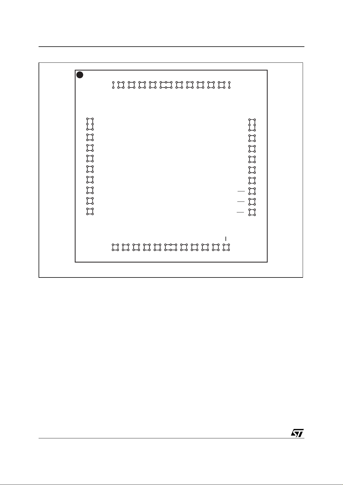
Figure 4. PBGA C on nec ti ons (Top View)
404139
A8
CC
V
V
1
CC
A7
2
A6
3
4
A5
5
GND
A4
6
7
A3
A2
8
9
A1
A0
DQ0
A9
DQ1
38
A10
DQ2
37
36
A11
GND
M48T254V
GND
DQ3
35
A12
34
A13
DQ4
33
A14
DQ5
32
A15
DQ6
31
A16
DQ7
30
V
BL
CC
V
CC
A17
A18
A19
GND
A20
CE
OE
WE
29
28
27
26
25
24
23
22
21
11
10
Note: Thi s di agram is TOP VI E W perspecti ve (view through package).
12
13
14
15
16
17
18
19
20
AI04216
4/24
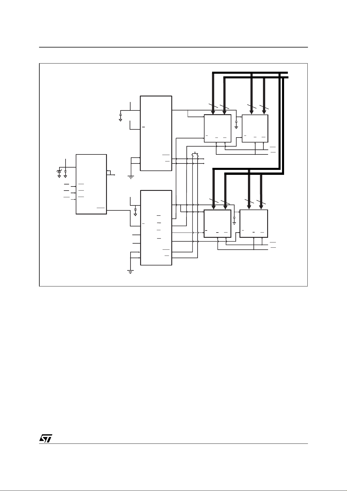
Figure 5. Hardware Hookup
3.3V
CE
OE
WE
M41T315V
V
CC
CEI
OE
WE
CEO
D
Q
DQ0
V
A19
A20
3.3V
OUT
3.3V
M40Z300W
V
CC
E
THS
V
SS
M40Z300W
V
CC
E
A
B
THS
V
SS
E1
E2
E3
E4
V
V
OUT
RST
BL
OUT
CON
CON
CON
CON
RST
BL
A0-A18
19
V
CC
M68Z512W
E
G
3.3V
(Not Bonded)
To Battery Monitor Circuitry
A0-A18
19
V
CC
M68Z512W
E
G
8
W
8
W
DQ0-DQ7
.1µF
DQ0-DQ7
V
.1µF
E
A0-A18
19
V
CC
M68Z512W
E
E
G
A0-A18
19
CC
M68Z512W
G
M48T254V
DQ0-DQ7
8
W
WE
OE
DQ0-DQ7
8
W
WE
OE
AI04215
5/24
M48T254V
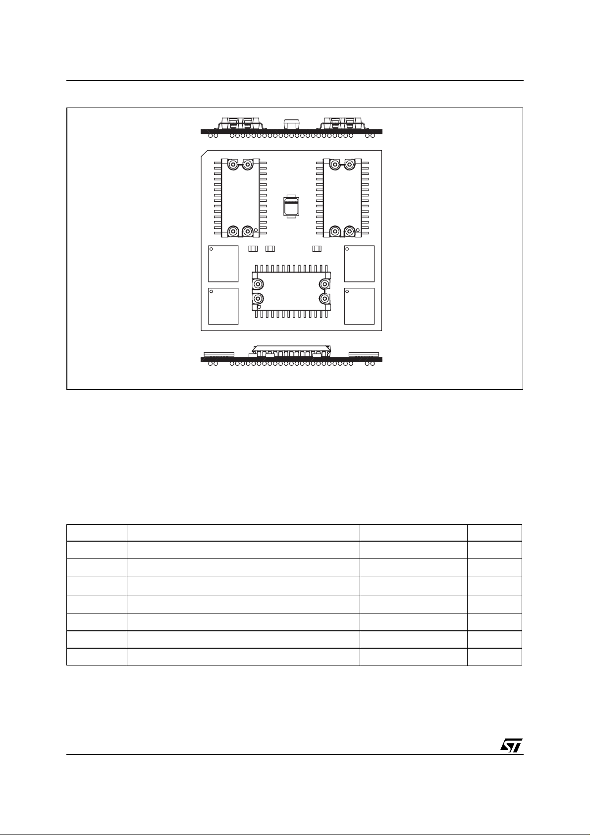
Figure 6. M4 8T2 54V PBGA Mod ul e So lu tion (Si de / Top)
AI04214b
MAXIMUM RATING
Stressing the device ab ove the rating listed in the
“Absolute Maximum Ratings” table may cause
permanent damage to the device. These are
stress ratings only and operation of the dev ice at
these or any other conditions above those indicat-
not implied. Exposure to Absol ute Maxim um Ra ting conditions for extended periods may affect device reliability. Refer also to the
STMicroelectronics SURE Program and other relevant quality documents.
ed in the Operating sections of this specification is
Table 2. Absolute Maximum Ratings
Symbol Parameter Value Unit
T
T
V
T
STG
SLD
CC
V
I
P
A
IO
O
D
Operating Temperature 0 to 70 °C
Storage Temperature (VCC, Oscillator Off)
Lead Solder Temperature for 10 seconds 260 °C
Supply Voltage (on any pin relative to Ground) –0.3 to +4.6 V
Input or Output Voltages
Output Current 20 mA
Power Dissipation 1 W
–40 to 85 °C
–0.3 to V
CC
+ 0.3
V
CAUTION! Negative undershoots be l ow –0.3V are not al lowed on any pin while in the Battery Back-up Mode.
6/24

DC AND AC PARAMETERS
This section summarizes the operat ing and measurement conditions, as well as the DC and AC
characteristics of the device. The parameters in
the following DC and AC Characteristic tables are
ment Conditions listed in the rel evant tables. Designers should check that the operating conditions
in their projects match the measurement conditions when using the quoted parameters.
derived from tests performed under the M easure-
Table 3. DC and AC Measurement Conditions
Parameter M41T254V
V
Supply Voltage
CC
Ambient Operating Temperature 0 to 70°C
Load Capacitance (C
Input Rise and Fall Times ≤ 5ns
Input Pulse Voltages 0 to 3V
Input and Output Timing Ref. Voltages 1.5V
Note: Out put Hi-Z is defined as the poin t where data is no l onger driven.
)
L
3.0 to 3.6V
50pF
Figure 7. AC Testing Load Circuit
M48T254V
DEVICE
645Ω
UNDER
TEST
CL = 50 pF
1.75V
AI04644
Table 4. Capacitance
Symbol
C
IN
C
OUT
(3)
C
IO
Note: 1. Effective capacitance measure d wi th power supply at 3V. Sampled only; not 100% tested.
2. At 25°C, f = 1MHz.
3. Outputs were dese l ected.
Input Capacitance (A0-A18, OE, WE, CE)40pF
Input Capacitance (A19-A20) 10 pF
Output Capacitance (BL)20pF
Input / Output Capacitance 40 pF
Parameter
(1,2)
Min Max Unit
7/24

M48T254V
Table 5. DC Characteristics
Sym Parameter
Test Condition
(1)
M48T254V
Unit
Min Typ Max
Input Leakage Current
I
LI
I
Output Leakage Current
LO
I
Supply Current 50 mA
CC1
I
Supply Current (TTL Standby)
CC2
I
VCC Power Supply Current CE = V
CC3
(2)
V
V
V
V
PFD
V
Note: 1. Valid fo r Ambient Operating Temperature: TA = 0 to 70°C; VCC = 3.0 to 3.6V (except where noted).
Input Low Voltage –0.3 0.6 V
IL
(2)
Input High Voltage 2.2
IH
Output Low Voltage (Open Drain)
(3)
OL
Output Low Voltage
V
Output High Voltage
OH
(2)
Power Fail Deselect 2.80 2.97 V
(2)
Battery Back-up Switchover
SO
2. All vol t ages are referenced to Ground.
3. For BL
pin (Open Drain).
0V ≤ V
0V ≤ V
OUT
CE
I
= 10mA
OL
= 2.0mA
I
OL
I
= –1.0mA
OH
IN
= V
CCI
≤ V
≤ V
IH
– 0.2
CC
CC
57mA
23mA
2.4 V
2.5
±4 µA
±4 µA
V
+ 0.3
CC
0.4 V
0.4 V
V
V
8/24

OPERATION MODES
READ
A READ cycle executes whenever WRITE Enable
) is high and Chip Enable (CE) is low (see Fig-
(WE
ure 8, page 10). The distinct address defined by
the 21 address inputs (A0-A20) specifies which of
the 2M bytes of data is to be accessed. Valid data
will be ac cessed by t he eight data output drivers
within the specified Access Time (t
last address input signal is stable, the CE
) after the
ACC
and OE
access times, and their respective parameters are
satisfied. When CE
t
ACC
and OE t
are not sat-
ACC
isfied, then data access times must be measured
from the more recent CE
limiting parameter being t
OE
) instead of address access.
and OE signals, with the
(for CE) or tOE (for
CO
Table 6. Operating Modes
Mode
Deselect
WRITE
READ
READ
Deselect
Deselect
Note: X = VIH or VIL; VSO = Battery B ack-up Switchover Voltage
1. See Table 8, page 13 for details.
V
V
3.0V to 3.6V
to V
SO
PFD
≤ V
SO
CC
(min)
(1)
(1)
CE OE WE DQ7-DQ0 Power
V
IH
V
IL
V
IL
V
IL
X X X High-Z CMOS Standby
X X X High-Z Ba ttery Back -Up
M48T254V
WRITE
WRITE Mode occurs whenever CE
nals are low (after address inputs are stable, see
Figure 9, page 10 and Figure 10, page 11). The
most recent falling edge of CE
mine when the WRITE cycle begins (the earlier,
rising edge of CE
or WE determines cycle termination). All address inputs must be kept stable
throughout the WRITE cycle. WE
active) for a minimum recovery time (t
subsequent cycle is initiated. The OE
nal should be kept high (inactive) during the
WRITE cycles to avoid bus contention. If CE
are low (active), WE will disable the outputs for
OE
Output Data WRITE Time (t
ODW
edge.
X X High-Z Standby
X
V
IL
V
IH
V
IL
V
IH
V
IH
D
IN
D
OUT
High-Z Active
and WE sig-
and W E will deter-
must be high (in-
) before a
WR
control sig-
and
) from i ts falling
Active
Active
9/24

M48T254V
Figure 8. Memory READ Cycle
ADDRESSES
CE
OE
DQ0 - DQ7
Note: WE is high for a READ cycle.
tCOE
tCOE
tACC
tCO
tRC
tOH
tOD
tOE
tODO
DATA OUTPUT
VALID
AI04230
Figure 9. Memory WRITE Cycle, WRITE Enable Controlled
ADDRESSES
tAW
CE
WE
tODW
HIGH IMPEDANCE
DQ0–DQ7
tWC
tWP
tDS
tAH1
tOEW
tDH1
DATA IN
STABLE
AI05655
Note: 1. OE = VIH or VIL. If OE = VIH during a WRI TE cycle, the output buffers remain in a high imp edance state.
2. If the CE
3. If th e CE
low transition occurs simultaneously with or later than the WE low transition in WE Controlled WRITE, the output buffers
remain in a high impedance st ate during thi s period.
high t rans ition o ccur s s imul tane ousl y w ith t he WE hi gh t ran sition , the outp ut b uffe rs r ema in i n a h igh impe dan ce s tat e
during this period.
10/24

Figure 10. Memory WRITE Cycle, Chip Enable Controlled
ADDRESSES
tAW
CE
tWC
tWP
M48T254V
tAH2
tOEW
WE
tCOE
DQ0–DQ7
Note: 1. OE = VIH or VIL. If OE = VIH during a WRI TE cycle, the output buffers remain in a high imp edance state.
is low or the WE low transition occurs prior to or simultaneously with the CE low transition, the output buffers remain in a high
2. If WE
impedance state during this period.
tODW
tDS tDH2
DATA IN
STABLE
AI05656
11/24

M48T254V
Table 7. AC Electrical Characteristics
Symbol
t
AVAV
t
AVQV
t
ELQV
t
GLQV
t
ELQX
t
AXQX
t
EHQZ t
t
GHQZ t
t
WLQZ t
t
AVAV
t
WLWH
t
ELEH
t
AVEL
t
WHAX
t
EHAX
t
WHQX
t
DVEH
t
DVWH
t
t
COE
OD
ODO
ODW
t
t
WP
t
t
t
t
OEW
t
RC
ACC
t
CO
t
OE
t
OH
WC
AW
AH1
AH2
t
DS
READ Cycle Time 100 ns
Access Time 100 ns
Chip Enable Low to Output Valid 100 ns
Output Enable Low to Output Valid 55 ns
(2)
Chip Enable or Output Enable Low to Output Transition 5 ns
Output Hold from Address Change 5 ns
(2)
Chip Enable High to Output Hi-Z 35 ns
(2)
Output Enable High to Output Hi-Z 35 ns
(2)
Output Hi-Z from WE 35 ns
WRITE Cycle Time 100 ns
(3)
WE, CE Pulse Width 70 ns
Address Setup Time 0 ns
Address Hold Time from WE 5ns
Address Hold Time from CE 25 ns
(2)
Output Active from WE 5ns
Data Setup Time 40 ns
Parameter
(1)
M48T254V
Unit
Min Max
t
WHDX
t
EHDX t
t
DH1
DH2
t
t
WR
Note: 1. Valid fo r Ambient Operating Temperature: TA = 0 to 70°C; VCC = 3.0 to 3.6V (except where noted).
2. These parameters are sampled wi th a 5 pF l oad are not 100% t est ed.
is specified as the logical AND of CE and WE. tWP is measured from the la tt er of CE or WE going low to the ea rlier of CE or
3. t
WP
going high .
WE
4. t
is a function of the latter occurring edge of WE or CE.
WR
Data Hold Time from WE 0ns
Data Hold Time from CE 20 ns
READ Recovery (Clock Access Only) 20 ns
RR
(4)
WRITE Recovery (Clock Access Only) 20 ns
12/24

Data Retention Mode
PFD
CC
(the
is
Data can be read or written only when V
greater than V
. When VCC is below V
PFD
point at which write protection occurs), the clock
registers and the SRAM are bloc ked from any access. When V
Over threshold (V
V
to battery backup (V
CC
falls below the Battery Switch
CC
), the device is switched from
SO
). RTC operation and
BAT
SRAM data are maintained via battery backup until power is stable. All control, data, and address
signals must be powered down when V
is pow-
CC
ered down.
Figure 11. Power Down/Up Mode AC Waveforms
V
CC
V
V
PFD
PFD
(max)
(min)
V
SO
tF
M48T254V
The lithium power source is designed to provide
power for RTC activity as well as RTC and RAM
data retention when V
The capa bility of this sour ce is s uffic ien t to pow er
the device continuously for th e life of the equipment into which it has been installed. For specification purposes, life expectancy is ten (10) years
at 25°C with the intern al os cillator running without
V
. The actual life expectancy will be much long-
CC
er if no battery e nergy is used (e.g., wh en V
present).
is absent or unstable.
CC
tR
CC
is
tFB
tPD
CE
DON'T CARE
tDR
Table 8. Power Down/Up Trip Points DC Characteristics
Symbol
t
REC
t
F
t
FB
t
R
t
PD
(2)
t
DR
Note: 1. Valid fo r Ambient Operating Temperature: TA = 0 to 70°C; VCC = 3.0 to 3.6V (except where noted).
2. At 25°C, V
(Requires use of three M4 T 32-BR12SH SNA PHAT
V
(max) to CE low
PFD
V
(max) to V
PFD
V
(min) to VSO VCC Fall Time
PFD
V
(min) to V
PFD
CE High to Power-Fail 0 µs
Expected Data Retention Time 10 Years
= 0V; the expected tDR is defined as cumulative time in the absence of VCC with the clock oscillator running.
CC
Parameter
(min) VCC Fall Time
PFD
(max) VCC Rise Time
PFD
(1)
®
tops .)
Min Max Unit
40 120 ms
300
10
0
tREC
AI05657
µs
µs
µs
13/24

M48T254V
PHANTOM CLOCK OPERATION
Communication with the Phantom Clock is established by pattern recogn ition of a serial bit-stream
of 64 bits which must be matched by executing 64
consecutive WRITE cycles containing the proper
data on DQ0.
All accesses which occur prior to recognition of the
64-bit pattern are directed to memory.
After recognition is established, the next 64 READ
or WRITE cycles either extract or update data in
the clock while disabling the memory.
Data transfer to and from the timekeeping function
is accomplished with a serial bit-stream under control of Chip Enable (CE
WRITE Enable (WE
the C E
and OE control of the clock starts the pa ttern recognition sequence by moving the pointer to
the first bit of the 64-bit comparison register (see
Figure 12, page 15).
Next, 64 consecutive WRITE cycles are execut ed
using the CE
and WE control of the device. These
64 WRITE cycles are used only to gain access to
the clock. Therefore, any addres s to the me mory
is acceptable. However, the WRITE cycles generated to gain access to the Phantom Clock are also
writing data to a location in the mated RAM. The
preferred way to manage this requirement is to set
), Output Enable (OE), and
). Initially , a READ cycle using
aside just one address location in RAM as a Phantom Clock scratch pad.
When the first WRITE cycle is executed, it is compared to Bit 1 of the 64-bit comparison register. If
a match is found, the pointer increments to the
next location of the comparison register and
awaits the next WRITE cycle.
If a match is not found, the pointer does not advance and all subsequent WRITE cycles are ignored. If a READ cycle occurs at any t ime during
pattern recognition, the present sequence is aborted and the comparison register pointer is reset.
Pattern recognition continues for a total of 64
WRITE cycles as described above until all of the
bits in the comparison register have been
matched. With a correct match for 64-bits, the
Phantom Clock is enabled and data t ransf er t o or
from the timekeeping registers can proceed. The
next 64 cycles will cause the Phantom Clock to either receive or transmit data on DQ0, depend ing
on the level of the OE
pin or the WE pin. Cycles to
other locations outside the memory block can be
interleaved with CE
cycles without interrupting the
pattern recognition sequence or dat a transfer sequence to the Phantom Clock.
14/24

Figure 12. Comparison Register Definition
65 432
1
0
BYTE 0
7
1
M48T254V
Hex
1
0
1
0
0
10
Value
C5
BYTE 1
BYTE 2
BYTE 3
BYTE 4
BYTE 5
BYTE 6
BYTE 7
0
1
0
1
0
1
0
0
0
1
1
0
0
1
1
1
0
0
1
1
0
1
0
1
0
1
0
1
0
0
1
1
0
0
1
1
1
0
0
1
1
0
01
10
01
10
01
10
01
3A
A3
5C
C5
3A
A3
5C
AI04262
Note: The odds of t his patter n being acc i dentally du pl i cated and sending aberrant ent ri es to the RTC is less than 1 in 1019. This pattern is
sent to the clock LSB to MSB.
15/24

M48T254V
Clock Register Information
Clock information is contained in eight registers of
8 bits, each of which is sequentially accessed one
(1) bit at a time after the 64-bit pattern recognition
sequence has been completed. When updating
the clock registers, each must be handled in
groups of 8 bits. Writing and reading individual bits
within a register could produce erroneous results.
These READ/WRITE registers are defined in the
clock register map (see Table 9).
Data contained in the clock regis ters is in Binary
Coded Decimal format (BCD). Reading and writing
the registers is always accom plished by stepping
through all eight registers, starting with Bit 0 of
Register 0 and ending with Bit 7 of Register 7.
AM-PM/12/2 4 Mo de
Bit 7 of the hours register is defined as the 12-hour
or 24-hour mode select bit. When it is high, the 12hour mode is selected. In the 12-hour mo de, Bit 5
is the AM/PM bit with the logic high being “PM.” In
the 24-hour mode, Bit 5 is the second 10-hour bit
(20-23 hours).
Oscillator Bit
Bit 5 controls the oscillat or. When set to logic '0 ,'
the oscillator turns on and the RTC/calendar begins to increment.
Zero Bits
Registers 1, 2, 3, 4, 5, and 6 contain one (1) or
more bits that will always read logic '0.' When writing to these locations, either a logic '1' or '0' is acceptable.
Table 9. RTC Register Map
Function/Range
Register D7 D6 D5 D4 D3 D2 D1 D0
0 0.1 Seconds 0.01 Seconds Seconds 00-99
1 0 10 Seconds Seconds Seconds 00-59
2 0 10 Minutes Minutes Minutes 00-59
3 12/24 0
400OSC
5 0 0 10 date Date: Day of the Month Date 01-31
10/
A/P
Hrs Hours (24 Hour Format) Hours
1 0 Day of the Week Day 01-7
BCD Format
01-12/
00-23
6 0 0 0 10M Month Month 01-12
7 10 Years Year Year 00-99
Keys:
A/P = AM/PM Bit
12/24 = 12 or 24-hour mode B i t
= Oscillator Bit
OSC
= Rese t B i t
RST
0 = Must be set to '0'
1 = Must be set to '1'
16/24

Figure 13. Phantom Clock READ Cycle
M48T254V
WE
tCW
tCO
CE
tOW
OE
tOEE
tCOE
Q
Figure 14. Phantom Clock WRITE Cycle
OE
tOE
tRC
tRR
tOD
tODO
DATA OUTPUT VALID
AI04259
tWC
WE
CE
D
tWP
tCW
tDS
DATA INPUT STABLE
tWR
tAH2
tDH2
tDH1
AI05658
17/24

M48T254V
Battery Low
The M48T254V automatically performs battery
voltage monitoring upon power-up, and at factoryprogrammed time intervals of at least 24 hours.
The Battery Low (BL
battery voltage is f ound to be less than approximately 2.5V. The BL
until completion of battery replacement and subsequent battery low monitoring tests, either during
the next power-up sequence or the next scheduled
24-hour interval.
If a battery low is generated during a power-up sequence, this indicates that one of the batteries is
below 2.5V and may not be ab le to maintain data
integrity in the SRAM. Data should be considered
suspect, and verified as correct. All three
SNAPHAT
®
tops should be replaced.
If a battery low indication is generated during the
24-hour interval check, this indicates that one of
the batteries is near end of lif e. However, data is
) signal will be asserted if t he
signal will remain asserted
not compromised due to the fact that a nominal
is supplied. In order to insure data integrity
V
CC
during subsequent periods of battery back-up
mode, the batteries should be replaced. The
SNAPHAT top should be replaced with valid V
CC
applied to the device.
The M48T254V onl y monitors the b atteries when
a nominal V
is applied to the device. Thus appli-
CC
cations which require extensive durations in the
battery back-up mode should be powered-up periodically (at least once every few months) in order
for this technique to be beneficial. Additionally, if a
battery low is indicated, data integrity should be
verified upon power-up via a checksum or other
technique. The BL
signal is an open d rain output
and an appropriate pull-up resistor should be chosen to control the rise time.
Note: The BL
signal is available only for the exter-
nal SRAM, not for the Real-Time Clock.
18/24

M48T254V
PART NUMBERING
Table 10. Ordering Information Scheme
Example: M48T 254V –10 ZA 1
Device Type
M48T
Supply Voltage and Write Protect Voltage
254V = V
Speed
–10 = 100ns
= 3.0 to 3.6V; V
CC
= 2.8 to 2.97V
PFD
Package
ZA = 42.5mm x 42.5mm
(1)
(2)
, 1.27mm Ball Pitch, BGA Module
Temperature Rang e
1 = 0 to 70°C
Note: 1. The SOIC packages (SO28/SO44) require the battery/crystal package (SNAPHAT) which is ordered separately under the part num-
ber “M4T3 2-B R12SH” in plastic tube or “M4T32-BR12SHTR” in Tape and Reel form.
2. Where “Z” is the symb ol for BGA packa ges and “A” denot es 1.27mm ball pitch
For a list of available options (e.g., Speed, Package) or for further information on any aspect of this device,
please contact the ST Sales Office nearest to you.
Table 11. SNAPHAT Battery Table
Part Number Description Package
M4T32-BR12SH Lithium Battery (120mAh) SNAPHAT SH
19/24

M48T254V
PACKAGE MECHANICAL INFORMATION
Figure 15. PBGA-ZA – 168-ball Plastic Ball Grid Array Package Outline
A
D
GD
B
JE
E
HE
FE
E E1
A3
B1
A
A1
A2
SIDE VIEW
(SH x 1)
B
HD
TOP VIEW
45˚
GE
PIN 1 CORNER
C
ddd
SIDE VIEW
(SH x 2)
eee
S
fff
e
DETAIL A
S
SS
A
B
C
C
b
e
Detail A
0.20 (4X)
Note: Drawing is not to scale.
20/24
b
e
D1
D
BOTT OM VIEW
SOLDER BALL (Typ)
FD
PBGA-Z02

Table 12. PBGA-ZA – 168-ball Plastic Ball Grid Array Package Mechanical Data
mm inches
Symb
Typ Min Max Typ Min Max
A 2.94 2.74 3.14 0.116 0.108 0.124
A1 0.89 0.69 1.0 9 0.035 0.027 0.043
A2 11.53 11.18 11.88 0.454 0.440 0.468
A3 7.24 8.0 0 0.285 0.315
B 3 8.54 38.34 38.74 1.517 1.509 1.525
B1 21.21 21.84 0.835 0.860
b 0.76 0.71 0.8 1 0.030 0.028 0.032
D 42.50 42.30 42.70 1.673 1.665 1 .681
D1 27.94 1.100
E 4 2.50 42.30 42.70 1.673 1.665 1.681
E1 22.86 0.900
e 1.27 0.050
FD 7.28 7.18 7.38 0.287 0.283 0 .291
FE 9.82 9.72 9.92 0.3 87 0.383 0.391
M48T254V
GD 1.75 1.55 1.95 0.069 0.061 0 .077
GE 1.50 1.30 1.70 0.0 59 0.051 0.067
HD 1.98 1.78 2.18 0.0 78 0.070 0.086
HE 0.51 0.31 0.7 1 0.020 0.012 0.028
JE 1.50 1.30 1.70 0.059 0.051 0 .067
n 168 168
Tolerance Tolerance
ddd 0.15 0.006
eee 0.30 0.012
fff 0.15 0.006
21/24

M48T254V
Figure 16. SH – 4-pin SNAPHAT Housing for 120mAh Battery & Crystal, Package Outline
A2
A3
L
eA
D
A1
A
B
eB
E
SHTK-A
Note: Drawing is not to scale.
Table 13. SH – 4-pin SNAPHAT Housing for 120mAh Battery & Crystal, Package Mechanical Data
Symb
Typ Min Max Typ Min Max
A 10.54 0.415
mm inches
A1 8.00 8.5 1 0.315 .0335
A2 7.24 8.0 0 0.285 0.315
A3 0.38 0.015
B 0.46 0.56 0.018 0.022
D 21.21 21.84 0.835 0.860
E 17.27 18.03 0.680 .0710
eA 15.55 15.95 0.612 0.628
eB 3.20 3.6 1 0.126 0.142
L 2.03 2.29 0.080 0.090
22/24

REVISION HIST ORY
Table 14. Document Revision History
Date Rev. # Revision Details
September 2002 1.0 First Issue
31-Mar-03 1.1 Updated test condition (Table 8)
19-May-03 2.0 v2.2 template update; modify package dimensions (Table 12)
M48T254V
23/24

M48T254V
Information furnishe d is bel i eved to be accurate and reliable. However, STMicroelectronics assumes no responsibility for the consequences
of use of such information nor for any infringement of patents or other rights of third parties which may result from its use. No license is granted
by implic ation or otherwise unde r any patent or patent rights of STMicroelectronics. Specifications me ntioned in th i s publication are subject
to change without notice. This publication supersedes and replaces all information previously supplied. STMicroelectronics products are not
authorized for use as crit i cal component s in l i fe support devi ces or systems wi t hout express written approv al of STMicroelec tronics.
The ST log o i s registered trademark of STM i croelectronics
All other names are the property of the i r respective owners.
© 2003 STMicroelectronics - All Rights Reserved
STMicroelectron ics GROUP OF COMPANIES
Australi a - Brazil - Cana da - China - Finland - France - Ger m any - Hong Kong - I ndi a - Israel - Italy - Japan - Malaysia -
Malta - Mor occo - Singapore - Spain - Sweden - Switzerland - United Ki ngdom - U.S.A .
www.st.com
24/24
 Loading...