

5.0 or 3.3V, 4096K TIMEKEEPER® SRAM with PHANTOM
FEATURES SUMMARY
■ 5.0V OR 3.3V OPERATING VOLTAGE
■ REAL TIME CLOCK KEEPS TRACK OF
TENTHS/HUNDREDTHS OF SECONDS,
SECONDS, MINUTES, HOURS, DAYS, DATE
OF THE MONTH, MONTHS, and YEARS
■ AUTOMATIC LEAP YEAR CORRECTION
VALID UP TO THE YEAR 2100
■ AUTOMATIC SWITCH-OVER and DESELECT
CIRCUITRY
■ CHOICE OF POWER-FAIL DESELECT
VOLTAGES:
= Power-fail Deselect Voltage):
(V
PFD
– M48T251Y: 4.25V
– M48T251V: 2.80V
■ FULL 10% V
■ OVER 10 YEARS’ DATA RETENTION IN THE
CC
≤ V
≤ V
OPERATING RANGE
ABSENCE OF POWER
■ WATCH FUNCTION IS TRANSPARENT TO
RAM OPERATION
■ 512K x 8 NV SRAM DIRECTLY REPLACES
VOLATILE STAT IC RA M OR EEPRO M
PFD
PFD
≤ 4.50V
≤ 2.97V
M48T251Y
M48T251V
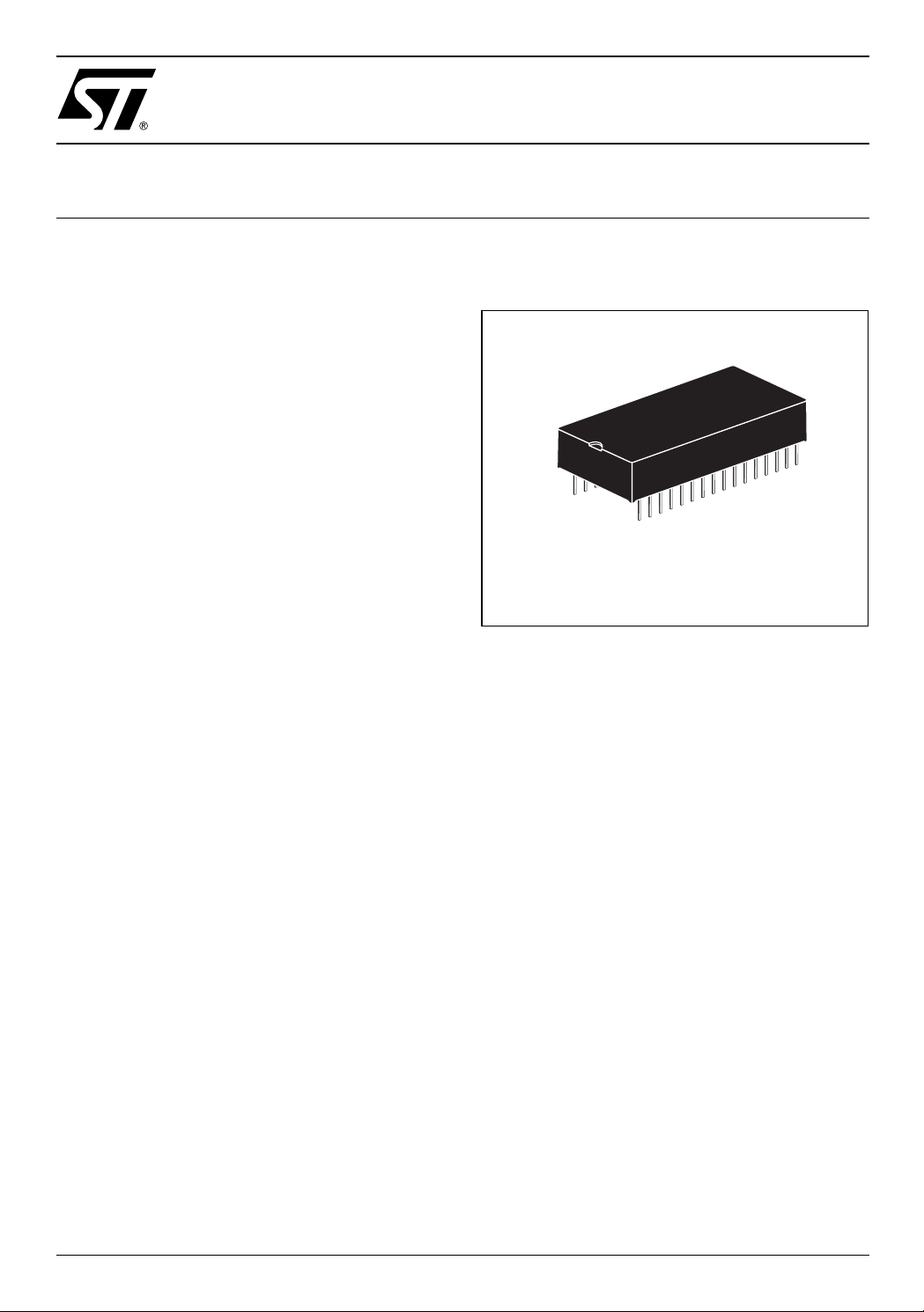
Figure 1. 32-pin, DIP Package
32
1
PMDIP32 (PM)
Rev. 2.0
1/24March 2003

M48T251Y, M48T251V
TABLE OF CONTENTS
SUMMARY DESCRIPTION. . . . . . . . . . . . . . . . . . . . . . . . . . . . . . . . . . . . . . . . . . . . . . . . . . . . . . . . . . . 4
Figure 2. Logic Diagram . . . . . . . . . . . . . . . . . . . . . . . . . . . . . . . . . . . . . . . . . . . . . . . . . . . . . . . . . . 4
Table 1. Signal Names . . . . . . . . . . . . . . . . . . . . . . . . . . . . . . . . . . . . . . . . . . . . . . . . . . . . . . . . . . . 4
Figure 3. DIP Connections . . . . . . . . . . . . . . . . . . . . . . . . . . . . . . . . . . . . . . . . . . . . . . . . . . . . . . . . 4
Figure 4. Block Diagram . . . . . . . . . . . . . . . . . . . . . . . . . . . . . . . . . . . . . . . . . . . . . . . . . . . . . . . . . . 5
MAXIMUM RATING. . . . . . . . . . . . . . . . . . . . . . . . . . . . . . . . . . . . . . . . . . . . . . . . . . . . . . . . . . . . . . . . . 6
Table 2. Absolute Maximum Ratings. . . . . . . . . . . . . . . . . . . . . . . . . . . . . . . . . . . . . . . . . . . . . . . . . 6
DC AND AC PARAMETERS. . . . . . . . . . . . . . . . . . . . . . . . . . . . . . . . . . . . . . . . . . . . . . . . . . . . . . . . . . 7
Table 3. DC and AC Measurement Conditions . . . . . . . . . . . . . . . . . . . . . . . . . . . . . . . . . . . . . . . . . 7
Figure 5. AC Testing Load Circuit . . . . . . . . . . . . . . . . . . . . . . . . . . . . . . . . . . . . . . . . . . . . . . . . . . . 7
Table 4. Capacitance. . . . . . . . . . . . . . . . . . . . . . . . . . . . . . . . . . . . . . . . . . . . . . . . . . . . . . . . . . . . . 7
Table 5. DC Characteristics. . . . . . . . . . . . . . . . . . . . . . . . . . . . . . . . . . . . . . . . . . . . . . . . . . . . . . . . 8
OPERATION MODES . . . . . . . . . . . . . . . . . . . . . . . . . . . . . . . . . . . . . . . . . . . . . . . . . . . . . . . . . . . . . . . 9
Table 6. Operating Modes. . . . . . . . . . . . . . . . . . . . . . . . . . . . . . . . . . . . . . . . . . . . . . . . . . . . . . . . . 9
READ . . . . . . . . . . . . . . . . . . . . . . . . . . . . . . . . . . . . . . . . . . . . . . . . . . . . . . . . . . . . . . . . . . . . . . . . 9
WRITE. . . . . . . . . . . . . . . . . . . . . . . . . . . . . . . . . . . . . . . . . . . . . . . . . . . . . . . . . . . . . . . . . . . . . . . . 9
Figure 6. Memory READ Cycle . . . . . . . . . . . . . . . . . . . . . . . . . . . . . . . . . . . . . . . . . . . . . . . . . . . . . 9
Figure 7. Memory WRITE Cycle 1 . . . . . . . . . . . . . . . . . . . . . . . . . . . . . . . . . . . . . . . . . . . . . . . . . .10
Figure 8. Memory WRITE Cycle 2 . . . . . . . . . . . . . . . . . . . . . . . . . . . . . . . . . . . . . . . . . . . . . . . . . .11
Table 7. Memory AC Characteristics, M48T251Y . . . . . . . . . . . . . . . . . . . . . . . . . . . . . . . . . . . . . . 12
Table 8. Memory AC Characteristics, M48T251V . . . . . . . . . . . . . . . . . . . . . . . . . . . . . . . . . . . . . . 13
Data Retention Mode. . . . . . . . . . . . . . . . . . . . . . . . . . . . . . . . . . . . . . . . . . . . . . . . . . . . . . . . . . . 14
Figure 9. Power Down/Up Mode AC Waveforms . . . . . . . . . . . . . . . . . . . . . . . . . . . . . . . . . . . . . . 14
Table 9. Power Down/Up Trip Points DC Characteristics . . . . . . . . . . . . . . . . . . . . . . . . . . . . . . . . 14
PHANTOM CLOCK OPERATION. . . . . . . . . . . . . . . . . . . . . . . . . . . . . . . . . . . . . . . . . . . . . . . . . . . . .15
Figure 10. Comparison Register Definition . . . . . . . . . . . . . . . . . . . . . . . . . . . . . . . . . . . . . . . . . . . 16
Clock Register Information. . . . . . . . . . . . . . . . . . . . . . . . . . . . . . . . . . . . . . . . . . . . . . . . . . . . . . 17
Clock Accuracy . . . . . . . . . . . . . . . . . . . . . . . . . . . . . . . . . . . . . . . . . . . . . . . . . . . . . . . . . . . . . . . 17
AM-PM/12/24 Mode . . . . . . . . . . . . . . . . . . . . . . . . . . . . . . . . . . . . . . . . . . . . . . . . . . . . . . . . . . . . 17
Oscillator and Reset Bits . . . . . . . . . . . . . . . . . . . . . . . . . . . . . . . . . . . . . . . . . . . . . . . . . . . . . . . 17
2/24

M48T251Y, M48T251V
Zero Bits. . . . . . . . . . . . . . . . . . . . . . . . . . . . . . . . . . . . . . . . . . . . . . . . . . . . . . . . . . . . . . . . . . . . . 17
Table 10. Phantom Clock Register Map . . . . . . . . . . . . . . . . . . . . . . . . . . . . . . . . . . . . . . . . . . . . . 17
Figure 11. Phantom Clock READ Cycle . . . . . . . . . . . . . . . . . . . . . . . . . . . . . . . . . . . . . . . . . . . . . 18
Figure 12. Phantom Clock WRITE Cycle . . . . . . . . . . . . . . . . . . . . . . . . . . . . . . . . . . . . . . . . . . . . 18
Figure 13. Phantom Clock Reset. . . . . . . . . . . . . . . . . . . . . . . . . . . . . . . . . . . . . . . . . . . . . . . . . . . 18
Table 11. Phantom Clock AC Characteristics (M48T251Y) . . . . . . . . . . . . . . . . . . . . . . . . . . . . . . 19
Table 12. Phantom Clock AC Characteristics (M48T251V) . . . . . . . . . . . . . . . . . . . . . . . . . . . . . . 20
PACKAGE MECHANICAL INFORMATION . . . . . . . . . . . . . . . . . . . . . . . . . . . . . . . . . . . . . . . . . . . . . 21
PART NUMBERING . . . . . . . . . . . . . . . . . . . . . . . . . . . . . . . . . . . . . . . . . . . . . . . . . . . . . . . . . . . . . . . 22
REVISION HISTORY. . . . . . . . . . . . . . . . . . . . . . . . . . . . . . . . . . . . . . . . . . . . . . . . . . . . . . . . . . . . . . . 23
3/24
M48T251Y, M48T251V
SUMMARY DESCRIPTION
®
The M48T251Y/V TIMEKEEPER
512Kbit x 8 non-volatile static RAM and real time
clock organized as 524 ,288 words by 8 bits. The
special DIP package provides a fully integrated
battery back-up memory and real time clock solution. In the event of power instability or absence, a
self-contained battery maintains the timekeeping
operation and provides po wer for a CMOS static
RAM. Control circuitry monitors V
write protection to prevent data c orruption in the
memory and RTC.
The clock keeps track of tenths/hundredths of seconds, seconds, minutes , hou rs, day, date, month,
RAM is a
and invokes
CC
and year information. The last day of the month is
automatically adjusted for months with less than
31 days, including leap year correction.
The clock operates in one of two formats:
– a 12-hour mode with an AM/PM indicator; or
– a 24-hour mode
The M48T251Y/V is a 32-pin (PM) DIP module
that integrates the RTC, the battery, and SRAM in
one package.
The modules are shipped in plastic, anti-static
tubes (see Table 14, page 22).
Figure 2. Logic Diagram Table 1. Signal Names
A0–A18 Address Input
RST
CE
OE
WE
Reset Input
Chip Enable
Output Enable Input
WRITE Enable Input
DQ0–DQ7 Data Inputs/Outputs
V
CC
V
SS
Supply Voltage Input
Ground
A0-A18
WE
CE
OE
V
CC
M48T251Y
M48T251V
DQ0-D7
RST
Figure 3. DIP C on ne ctions
V
30
29
28
27
26
25
24
23
22
20
19
18
17
32
31
21
CC
A15
A17
WE
A13
A8
A9
A11
OE
A10
CE
DQ7
DQ6
DQ5
DQ4
DQ3
AI04239
V
SS
AI04237
A18/RST
A16
A14
A12
DQ0
DQ1
DQ2
V
SS
A6
A5
A4
A3
A2
A0
A7
A1
1
2
3
4
5
6
7
8
9
10
11
12
13
14
15
16
M48T251Y
M48T251V
4/24
Figure 4. Block Diagram
M48T251Y, M48T251V
CE
OE
WE
RST
DQ0
CONTROL
LOGIC
ACCESS
ENABLE
SEQUENCE
DETECTOR
I/O
BUFFERS
32.768 Hz
CRYSTAL
READ
WRITE
POWER
FAIL
DATA
XO
XI
CLOCK/CALENDAR
LOGIC
UPDATE
TIMEKEEPER
REGISTER
SRAM
COMPARISON
REGISTER
INTERNAL V
CC
A0–A16
DQ0–DQ7
V
CC
POWER-FAIL
DETECT
LOGIC
V
BAT
AI04238
5/24
M48T251Y, M48T251V
MAXIMUM RATI N G
Stressing the device ab ove the rating listed in t he
“Absolute Maximum Ratings” table may cause
permanent damage to the device. These are
stress ratings only and operation of the dev ice at
these or any other conditions above those indicated in the Operating sections of this specification is
Table 2. Absolute Maximum Ratings
Symbol Parameter Value Unit
T
A
T
STG
(1)
T
SLD
V
CC
V
IO
I
O
P
D
Note: 1. Soldering temperature not to exceed 260°C for 10 seconds (total thermal budget not to exceed 150°C for longer than 30 seconds).
CAUTION! Negative undershoots below -0.3V are not al l owed on any pi n while in th e B attery Back-up Mod e .
Operating Temperature 0 to 70 °C
Storage Temperature (VCC, Oscillator Off)
Lead Solder Temperature for 10 seconds 260 °C
Supply Voltage (on any
pin relative to Ground)
Input or Output Voltages
Output Current 20 mA
Power Dissipation 1 W
not implied. Exposure to Absol ute Maxim um Ra ting conditions for extended periods may affect device reliability. Refer also to the
STMicroelectronics SURE Program and other relevant quality documents.
–40 to 85 °C
M48T251Y –0.3 to +7.0 V
M48T251V –0.3 to +4.6 V
–0.3 to V
CC
+ 0.3
V
6/24
M48T251Y, M48T251V
DC AND AC PARAMETERS
This section summarizes the operat ing and measurement conditions, as well as the DC and AC
characteristics of the device. The parameters in
the following DC and AC Characteristic tables are
derived from tests performed under the M easure-
Table 3. DC and AC Measurement Conditions
Parameter M48T251Y M48T251V
V
Supply Voltage
CC
Ambient Operating Temperature 0 to 70°C 0 to 70°C
Load Capacitance (C
Input Rise and Fall Times ≤ 5ns ≤ 5ns
Input Pulse Voltages 0 to 3V 0 to 3V
Input and Output Timing Ref. Voltages 1.5V 1.5V
Note: Out put Hi gh Z is defined as the poi nt where dat a i s no longer driven (see Table 3, page 7).
)
L
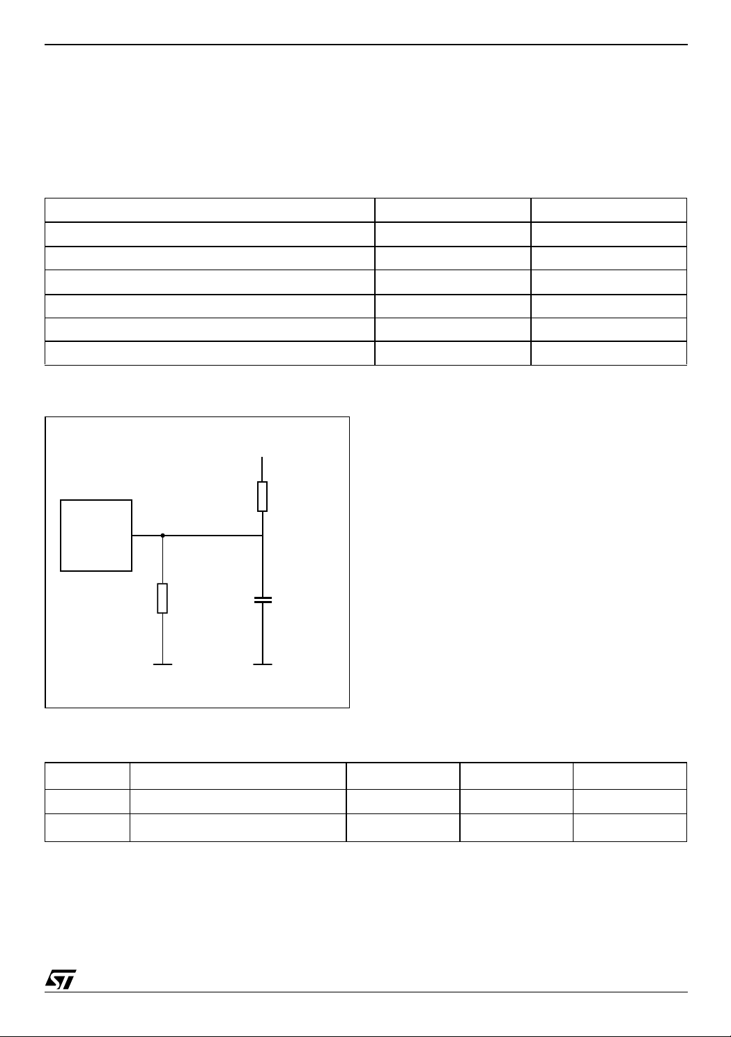
Figure 5. AC Testing Load Circuit
ment Conditions listed in the rel evant tables. Designers should check that the operating conditions
in their projects match the measurement conditions when using the quoted parameters.
4.5 to 5.5V 3.0 to 3.6V
100pF 50pF
V
CCI
1.1 KΩ
DEVICE
UNDER
TEST
680 Ω
Note: 50pF f or M48T251V.
CL = 50 pF
AI04240
Table 4. Capacitance
Symbol
C
IN
(3)
C
IO
Note: 1. Effective capacit ance meas ured with po wer supp l y at 5V . S am pled onl y; not 100% tested.
2. At 25°C, f = 1MHz.
3. Outpu ts were deselected.
Input Capacitance 10 pF
Input / Output Capacitance 10 pF
Parameter
(1,2)
Min Max Unit
7/24
M48T251Y, M48T251V
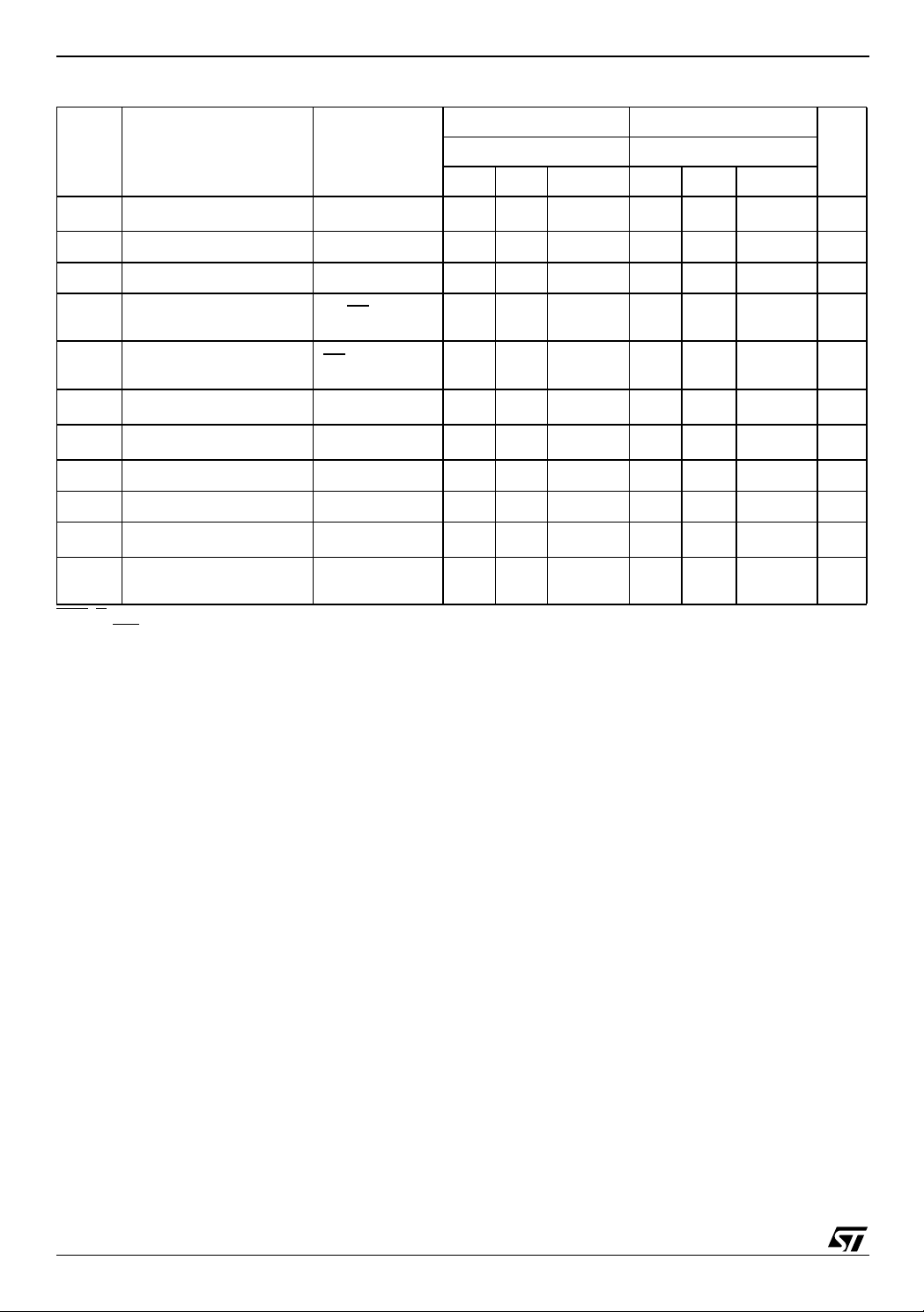
Table 5. DC Characteristics
M48T251Y M48T251V
Sym
(2)
I
LI
I
LO
I
CC1
I
CC2
I
CC3
(3)
V
IL
(3)
V
IH
V
OL
V
OH
(3)
V
PFD
(3)
V
SO
Note: 1. Valid fo r A m bi ent Operating Temperature: TA = 0 to 70°C; VCC = 4.5 to 5.5V or 3. 0 to 3.6V (except wher e not ed).
2. RST
3. All voltages are referenced to Ground.
Parameter
Input Leakage Current
Output Leakage Current
Supply Current 85 50 mA
Supply Current (TTL
Standby)
VCC Power Supply
Current
Input Low Voltage –0.3 0.8 –0.3 0.6 V
Input High Voltage 2.2
Output Low Voltage
Output High Voltage
Power Fail Deselect 4.25 4.37 4.50 2.80 2.97 V
Battery Back-up
Switchover
(Pin 1) has an i nternal pu l l-up resistor.
(1)
Test Condition
0V ≤ V
0V ≤ V
CE
I
IN
OUT
= V
CE
= V
CCI
I
= 2.0 mA
OL
= –1.0 mA
OH
≤ V
≤ V
IH
– 0.2
Min Typ Max Min Typ Max
CC
CC
±1 ±1 µA
±1 ±1 µA
510 5 7mA
35 23mA
V
CC
+ 0.3
2.2
0.4 0.4 V
2.4 2.4 V
V
BAT
2.5 V
VCC + 0.3
Unit–70 –85
V
8/24

OPERATION MODES
Table 6. Operating Modes
Mode
Deselect
WRITE
READ
READ
Deselect
Deselect
Note: X = VIH or VIL; VSO = Battery B ack-up Switchover Vo l tage
1. See Tab l e 9, page 14 for details.
V
V
4.5V to 5.5V
or
3.0V to 3.6V
to V
SO
PFD
≤ V
CC
SO
(min)
(1)
(1)
CE OE WE DQ7-DQ0 Power
V
IH
V
IL
V
IL
V
IL
X X X High-Z CMOS Standby
X X X High-Z Ba ttery Back -Up
M48T251Y, M48T251V
X X High-Z Standby
X
V
IL
V
IH
V
IL
V
IH
V
IH
D
IN
D
OUT
High-Z Active
Active
Active
READ
A READ cycle executes whenever WRITE Enable
) is high and Chip Enable (CE) is low (see Fig-
(WE
ure 6). The distinct address de fined by the 19 address inputs (A0-A18) specifies which of the 512K
bytes of data is to be access ed. Valid dat a will be
accessed by the eight data output drivers within
the specified Access Tim e (t
dress input signal is stable, the CE
) after the last ad-
ACC
and OE access
times, and their respective parameters are satisfied. When CE
and OE t
ACC
are not satisfied,
ACC
t
then data access times mus t be measured from
the more recent CE
ing parameter being t
and OE signals, with the limit-
(for CE) or tOE (for OE) in-
CO
stead of address access.
Figure 6. Memory READ Cycle
ADDRESSES
tACC
tCO
CE
tOE
WRITE
WRITE Mode (see Figure 7, page 10 and Figure 8,
page 11) occurs whenever CE
and WE signals are
low (after address inputs are stable). The most recent falling edge of CE
and WE will determine
when the WRITE cycle begins (the earlier, rising
edge of CE
or WE determines cycle termination).
All address inputs must be kept stable t hroughout
the WRITE cycle. WE
minimu m reco very t ime (t
cycle is in it iat e d. The OE
must be high (inactive) for a
) before a subsequent
WR
control signal should be
kept high (inactive) during the WRITE cycles to
avoid bus contention. If CE
tive), WE
will disable the outputs for Output Data
WRITE Time (t
tRC
) from its fa lling edge.
ODW
tOH
and OE are low (ac-
tOD
OE
DQ0 - DQ7
Note: WE is high for a READ cycle.
tCOE
tCOE
tODO
DATA OUTPUT
VALID
AI04230
9/24

M48T251Y, M48T251V
Figure 7. Memory WRITE Cycle 1
ADDRESSES
CE
tWC
tAW
tWR
tWP
WE
tODW
HIGH IMPEDANCE
DQ0–DQ7
Note: 1. OE = VIH or VIL. If OE = VIH during a WRI TE cycle, the output buff ers remain i n a hi gh impedance state.
2. If the CE
3. If th e C E
low transit i on occurs sim ul taneously with or later than the WE low transition in WRI T E Cycle 1, the out put buffers rem ain
in a high impedance state during th i s period.
high t rans ition o ccur s s imul tane ousl y w ith the W E h igh tran sit ion , the ou tput b uffe rs r ema in in a h igh impe dan ce s tat e
during this period.
tDS
tOEW
tDH
DATA IN
STABLE
AI04231
10/24

Figure 8. Memory WRITE Cycle 2
WE = V
IH
ADDRESSES
CE
V
IH
V
IL
tAW
M48T251Y, M48T251V
tWC
V
V
IH
IH
V
V
IL
IL
tWP
V
IH
V
IL
V
tWR
V
IH
IL
tOEW
WE
V
IL
V
IL
tODW
tCOE
DQ0–DQ7
tDS
V
IH
V
IL
DATA IN
STABLE
tDH
V
IH
V
IL
Note: 1. OE = VIH or VIL. If OE = VIH during a WRI TE cycle, the output buff ers remain i n a hi gh impedance state.
is low or the WE low transition occurs prior to or simultaneously with the CE low transition, the output buffers remain in a high
2. If WE
impedance state during this period.
AI04232
11/24

M48T251Y, M48T251V
Table 7. Memory AC Characteristics, M48T251Y
Symbol
t
AVAV
t
AVQV
t
ELQV
t
GLQV
t
ELQX
t
GLQX
t
AXQX
t
EHQZ
t
GHQZ
t
WLQZ t
t
AVAV
t
WLWH
t
ELEH
t
AVEL
t
AVWL
t
EHAX
t
WHAX
t
RC
t
ACC
t
CO
t
OE
t
COE
tOH
t
OD
ODW
t
WC
t
WP
t
AW
t
WR1
t
WR2
READ Cycle Time 70 ns
Access Time 70 ns
Chip Enable Low to Output Valid 70 ns
Output Enable Low to Output Valid 35 ns
Chip Enable or Output Enable Low to Output Transition 5 ns
Output Hold from Address Change 5 ns
(2)
Chip Enable or Output Enable High to Output Hi-Z 25 ns
(2)
Output Hi-Z from WE 25 ns
WRITE Cycle Time 70 ns
(3)
WE, CE Pulse Width 50 ns
Address Setup Time 0 ns
WRITE Recovery Time 15 ns
Address Hold Time from WE 0ns
Parameter
(1)
M48T251Y–70
Unit
Min Max
t
WHQX
t
DVEH
t
DVWH
t
WHDX
t
EHDX
Note: 1. Valid fo r A m bient Operating Temperature: TA = 0 to 70°C; VCC = 4.5 to 5.5V or 3. 0 to 3.6V (except wher e not ed).
2. These parameters are sampl ed with a 5 pF load are not 100% tested.
3. t
4. t
t
OEW
t
DS
t
DH1
t
DH2
is specified as the logical AND of CE and WE. tWP is measured f rom the l atter of CE or WE going low to the earl ier of CE or
WP
going high .
WE
and tDS are measured from the earlier of CE or WE going high.
DH
Output Active from WE 5ns
(4)
Data Setup Time 30 ns
(4)
Data Hold Time from WE 0ns
(4)
Data Hold Time from CE 10 ns
12/24

Table 8. Memory AC Characteristics, M48T251V
Symbol
t
AVAV
t
AVQV
t
ELQV
t
GLQV
t
ELQX
t
GLQX
t
AXQX
t
EHQZ
t
GHQZ
t
WLQZ t
t
AVAV
t
WLWH
t
ELEH
t
AVEL
t
AVWL
t
EHAX t
t
WHAX
t
t
ACC
t
t
t
COE
t
t
OD
ODW
t
t
WP1
t
WP2
t
WR1
t
WR2
RC
CO
OE
OH
WC
AW
READ Cycle Time 85 ns
Access Time 85 ns
Chip Enable Low to Output Valid 85 ns
Output Enable Low to Output Valid 45 ns
Chip Enable or Output Enable Low to Output Transition 5 ns
Output Hold from Address Change 5 ns
(2)
Chip Enable or Output Enable High to Output Hi-Z 35 ns
(2)
Output Hi-Z from WE 30 ns
WRITE Cycle Time 85 ns
(3)
WRITE Enable Pulse Width 65 ns
Chip Enable Pulse Width 75 ns
Address Setup Time 0 ns
(4)
WRITE Recovery Time 15 ns
Address Hold Time from WE 5ns
Parameter
(1)
M48T251Y, M48T251V
M48T251V–85
Unit
Min Max
t
WHQX
t
DVEH
t
DVWH
t
WHDX
t
EHDX
Note: 1. Valid fo r A m bient Operating Temperature: TA = 0 to 70°C; VCC = 4.5 to 5.5V or 3. 0 to 3.6V (except wher e not ed).
2. These parameters are sampl ed with a 5 pF load are not 100% tested.
3. t
4. t
5. t
t
OEW
t
DS
t
DH1
t
DH2
is specified as the logical AND of CE and WE. tWP is measured f rom the l atter of CE or WE going low to the earl ier of CE or
WP
WE
going high .
is a function of the latter occurring edge of WE or CE .
WR
and tDS are measured from the earlier of CE or WE going high.
DH
Output Active from WE 5ns
(5)
Data Setup Time 35 ns
(5)
Data Hold Time from WE 0ns
Data Hold Time from CE 15 ns
13/24

M48T251Y, M48T251V
Data Retention Mode
Data can be read or written only when V
greater than V
. When VCC is below V
PFD
point at which write protection occurs), the clock
registers and the SRAM are bloc ked from any access. When V
Over threshold (V
V
to battery backup (V
CC
falls below the Battery Switch
CC
), the device is switched from
SO
). RTC operation and
BAT
SRAM data are maintained via battery backup until power is stable. All control, data, and address
signals must be powered down when V
CC
ered down.
The lithium power source is designed to provide
power for RTC activity as well as RTC and RAM
Figure 9. Power Down/Up Mode AC Waveforms
V
CC
V
(max)
PFD
V
(min)
PFD
is
CC
(the
PFD
is pow-
tF
data retention when V
is absent or unstable.
CC
The capa bility of this sour ce is s uffic ien t to pow er
the device continuously for th e life of the equipment into which it has been installed. For specification purposes, life expectancy is ten (10) years
at 25°C with the intern al os cillator running without
. Each unit is shipped with its energy source
V
CC
disconnected, guaranteeing full energy capacity.
When V
V
PFD
is first applied at a level greater than
CC
, the energy source is enabled for battery
backup operation. The actual life expectancy will
be much longer if no ba ttery en ergy i s us ed (e. g.,
when V
is present).
CC
tR
V
SO
tFB
tPD
CE
tDR
tREC
Table 9. Power Down/Up Trip Points DC Characteristics
Symbol
t
REC
t
F
t
FB
t
R
t
PD
(2)
t
DR
Note: 1. Valid fo r A m bient Operating Temperature: TA = 0 to 70°C; VCC = 4.5 to 5.5V or 3. 0 to 3.6V (except wher e not ed).
2. At 25°C, V
V
(max) to CE low
PFD
V
(max) to V
PFD
V
(min) to VSO VCC Fall Time
PFD
V
(min) to V
PFD
CE High to Power-Fail 0 µs
Expected Data Retention Time 10 Years
= 0V; the expected tDR is defined as cumulative time in the absence of VCC with the clock oscillator running.
CC
Parameter
(min) VCC Fall Time
PFD
(max) VCC Rise Time
PFD
(1)
Min Max Unit
1.5 2.5 ms
300
10
0
AI04236
µs
µs
µs
14/24

PHANTOM CLOCK OPERATION
Communication with the Phantom Clock is established by pattern recogn ition of a serial bit-stream
of 64 bits which must be matched by executing 64
consecutive WRITE cycles containing the proper
data on DQ0.
All accesses which occur prior to recognition of the
64-bit pattern are directed to memory.
After recognition is established, the next 64 READ
or WRITE cycles either extract or update data in
the clock while disabling the memory.
Data transfer to and from the timekeeping function
is accomplished with a serial bit-stream under control of Chip Enable (CE
WRITE Enable (WE
the C E
and OE control of the clock starts the pat-
), Output Enable (OE), and
). Initially , a READ cycle using
tern recognition sequence by moving the pointer to
the first bit of the 64-bit comparison register (see
Figure 10, page 16).
Next, 64 consecutive WRITE cycles are execut ed
using the CE
and WE control of the device. These
64 WRITE cycles are used only to gain access to
the clock. Therefore, any addres s to the me mory
is acceptable. However, the WRITE cycles generated to gain access to the Phantom Clock are also
writing data to a location in the mated RAM. The
preferred way to manage this requirement is to set
M48T251Y, M48T251V
aside just one address location in RAM as a Phantom Clock scratch pad.
When the first WRITE cycle is executed, it is compared to Bit 1 of the 64-bit comparison register. If
a match is found, the pointer increments to the
next location of the comparison register and
awaits the next WRITE cycle.
If a match is not found, the pointer does not advance and all subsequent WRITE cycles are ignored. If a READ cycle occurs at any t ime during
pattern recognition, the present sequence is aborted and the comparison register pointer is reset.
Pattern recognition continues for a total of 64
WRITE cycles as described above until all of the
bits in the comparison register have been
matched. With a correct match for 64-bits, the
Phantom Clock is enabled and d ata trans fer t o or
from the timekeeping registers can proceed. The
next 64 cycles will cause the Phantom Clock to either receive or transmit data on DQ0, depend ing
on the level of the OE
other locations outside the memory block can be
interleaved with CE
pattern recognition sequence or dat a transfer sequence to the Phantom Clock.
pin or the WE pin. Cycles to
cycles without interrupting the
15/24

M48T251Y, M48T251V
Figure 10. Comparison Register Definition
65 432
1
0
BYTE 0
7
1
Hex
1
0
1
0
0
10
Value
C5
BYTE 1
BYTE 2
BYTE 3
BYTE 4
BYTE 5
BYTE 6
BYTE 7
0
1
0
1
0
1
0
0
0
1
1
0
0
1
1
1
0
0
1
1
0
1
0
1
0
1
0
1
0
0
1
1
0
0
1
1
1
0
0
1
1
0
01
10
01
10
01
10
01
3A
A3
5C
C5
3A
A3
5C
AI04262
Note: The odds of t his pattern bei ng accidentally duplicated and sending aberrant entries to the RTC is l ess tha n 1 in 1019. This pattern is
sent to the clock LSB to MSB.
16/24

M48T251Y, M48T251V
Clock Register Information
Clock information is contained in eight registers of
8 bits, each of which is sequentially accessed one
(1) bit at a time after the 64-bit pattern recognition
sequence has been completed. When updating
the clock registers, each must be handled in
groups of 8 bits. Writing and reading individual bits
within a register could produce erroneous results.
These READ/WRITE registers are defined in the
clock register map (see Table 10).
Data contained in the clock regis ters is in Binary
Coded Decimal format (BCD). Reading and writing
the registers is always accom plished by stepping
through all eight registers, starting with Bit 0 of
Register 0 and ending with Bit 7 of Register 7.
Clock Accuracy
The RTC is guaranteed to keep time ac curacy to
with ±1 minute per month at 25°C. The clock is factory-tuned with special calibration elements, and
does not require addition al calibration. Moderate
temperature deviation will have a negligible effect
in most applic a t ions.
Table 10. Phantom Clock Register Map
AM-PM/12/24 Mode
Bit 7 of the hours register is defined as the 12-hour
or 24-hour mode select bit. When it is high, the 12hour mode is selected. In the 12-hour mo de, Bit 5
is the AM/PM bit with the logic high being “PM.” In
the 24-hour mode, Bit 5 is the second 10-hour bit
(20-23 hours).
Oscillator and Reset Bits
Bits 4 and 5 of the day register are used to control
the reset and oscillator functions. Bit 4 controls the
reset pin input. When the reset bit is set to logic '1,'
the Reset Input pin is ignored. When the reset bit
logic is set to '0,' a low input on the reset pi n will
cause the device to abort data transfer without
changing data in the timekeeping registers. Reset
operates independently of all other inputs. Bit 5
controls the oscillator. When set to logic '0,' the oscillator turns on and the RT C/calendar begins to
increment.
Zero Bits
Registers 1, 2, 3, 4, 5, and 6 contain one (1) or
more bits that will always read logic '0.' When writing to these locations, either a logic '1' or '0' is acceptable.
Function/Range
Register D7 D6 D5 D4 D3 D2 D1 D0
0 0.1 Seconds 0.01 Seconds Seconds 00-99
1 0 10 Seconds Seconds Seconds 00-59
2 0 10 Minutes Minutes Minutes 00-59
3 12/24 0
400OSC
5 0 0 10 date Date: Day of the Month Date 01-31
6 0 0 0 10M Month Month 01-12
7 10 Years Year Year 00-99
Keys: A/P = AM/PM Bit
12/24 = 12 or 24-hour mode Bit
= Oscillator Bit
OSC
10 /
A/P
Hrs Hours (24 Hour Format) Hours
RST 0 Day of the Week Day 01-7
= Rese t B i t
RST
0 = Must be set to '0'
BCD Format
01-12/
00-23
17/24

M48T251Y, M48T251V
Figure 11. Phantom Clock READ Cycle
WE
tCW
tCO
CE
tOW
OE
tOEE
tCOE
Q
Figure 12. Phantom Clock WRITE Cycle
OE
tOE
tRC
tRR
tOD
tODO
DATA OUTPUT VALID
AI04259
tWC
WE
CE
D
Figure 13. Phantom Clock Reset
RST
tWP
tCW
tDS
DATA INPUT STABLE
tRST
tWR
tWR
tDH
t
DH
AI04261
AI04235
18/24

M48T251Y, M48T251V
Table 11. Phantom Clock AC Characteristics (M48T251Y)
Symbol
t
AVAV
t
ELQV
t
GLQV
t
ELQX
t
GLQX
t
EHQZ
t
GHQZ
t
AVAV
t
WLWH t
t
EHAX
t
DVEH
t
WHDX
t
EHDX
t
ELEH
Note: 1. Valid fo r A m bient Operating Temperature: TA = 0 to 70°C; VCC = 4.5 to 5.5V or 3. 0 to 3.6V (except wher e not ed).
2. These parameters are sampl ed with a 5 pF load and are not 100% tested.
3. t
4. t
5. t
t
t
t
t
COE
t
OEE
t
OD
t
ODO
t
t
WP
t
WR
t
DS
t
DH1
t
DH2
t
t
RST
is specified as the logical AND of CE and WE. tWP is measured f rom the l atter of CE or WE going low to the earl ier of CE or
WP
going high .
WE
is a function of the latter occurring edge of WE or CE .
WR
and tDS are measured from the earlier of CE or WE going high.
DH
READ Cycle Time 65 ns
RC
CE Access Time 55 n s
CO
OE Access Time 55 ns
OE
CE to Output Low Z 5 ns
OE to Output Low Z 5 ns
(2)
CE to Output High Z 25 ns
(2)
OE to Output High Z 25 ns
READ Recovery 10 ns
RR
WRITE Cycle Time 65 ns
WC
(3)
WRITE Pulse Width 55 ns
(4)
WRITE Recovery 10 ns
(5)
Data Setup Time 30 ns
(5)
Data Hold Time from WE 0ns
(5)
Data Hold Time from CE 0ns
CE Pulse Width 55 n s
CW
RST Pulse Width 65 ns
Parameter
(1)
Min Typ Max U nit
19/24

M48T251Y, M48T251V
Table 12. Phantom Clock AC Characteristics (M48T251V)
Symbol
t
AVAV
t
ELQV
t
GLQV
t
ELQX
t
GLQX
t
EHQZ
t
GHQZ
t
AVAV
t
WLWH t
t
EHAX
t
DVEH
t
WHDX
t
EHDX
t
ELEH
Note: 1. Valid fo r A m bient Operating Temperature: TA = 0 to 70°C; VCC = 4.5 to 5.5V or 3. 0 to 3.6V (except wher e not ed).
2. These parameters are sampl ed with a 5 pF load and are not 100% tested.
3. t
4. t
5. t
t
t
t
t
COE
t
OEE
t
OD
t
ODO
t
t
WP
t
WR
t
DS
t
DH1
t
DH2
t
t
RST
is specified as the logical AND of CE and WE. tWP is measured f rom the l atter of CE or WE going low to the earl ier of CE or
WP
going high .
WE
is a function of the latter occurring edge of WE or CE .
WR
and tDS are measured from the earlier of CE or WE going high.
DH
READ Cycle Time 85 ns
RC
CE Access Time 85 n s
CO
OE Access Time 85 ns
OE
CE to Output Low Z 5 ns
OE to Output Low Z 5 ns
(2)
CE to Output High Z 30 ns
(2)
OE to Output High Z 30 ns
READ Recovery 20 ns
RR
WRITE Cycle Time 85 ns
WC
(3)
WRITE Pulse Width 60 ns
(4)
WRITE Recovery 20 ns
(5)
Data Setup Time 35 ns
(5)
Data Hold Time from WE 0ns
(5)
Data Hold Time from CE 0ns
CE Pulse Width 65 n s
CW
RST Pulse Width 85 ns
Parameter
(1)
Min Typ Max U nit
20/24

PACKAGE MECHANICAL INFORMATION
Figure 14. PMDIP32 – 32-pin Plastic Module DIP, Package Outline
M48T251Y, M48T251V
A1AL
S
Be1
eA
e3
D
N
E
1
Note: Drawing is not to scale.
Table 13. PMDIP32 – 32-pin Plastic Module DIP, Package Mechanical Data
Symb
Typ Min Max Typ Min Max
A 9.27 9.52 0.365 0.375
A1 0.38 – 0.015 –
B 0.43 0.59 0.017 0.023
C 0.20 0.33 0.008 0.013
mm inches
C
PMDIP
D 42.42 43 .18 1.670 1.700
E 18.03 18.80 0.710 0.740
e1 2 .29 2.79 0.090 0.110
e3 34.29 41.91 1.350 1.650
eA 14.99 16.00 0.5 90 0.630
L 3 .05 3.81 0.120 0.150
S 1.91 2.79 0.075 0.110
N3232
21/24

M48T251Y, M48T251V
PART NUMBERING
Table 14. Ordering Information Example
Example: M48T 251Y –70 PM 1 TR
Device Type
M48T
Supply Voltage and Write Protect Voltage
251Y = V
251V = V
Speed
–70 = 70ns (M48T251Y)
–85 = 85ns (M48T251V)
= 4.5 to 5.5V; V
CC
= 3.0 to 3.6V; V
CC
= 4.25 to 4.50V
PFD
= 2.80 to 2.97V
PFD
Package
PM = PMDIP32
Temperature Rang e
1 = 0 to 70°C
Shipping Method for SOIC
blank = Tubes
TR = Tape & Reel
For a list of available options (e.g., Speed, Package) or for further information on any aspect of this device,
please contact the ST Sales Office nearest to you.
22/24

REVISION HIST ORY
Table 15. Document Revision History
Date Rev. # Revision Details
June 2001 1.0 First Issue
20-May-02 1.1 Add countries to disclaimer
28-Mar-03 2.0 v2.2 template applied; test condition updated (Table 9)
M48T251Y, M48T251V
23/24

M48T251Y, M48T251V
M48T251 , M48T251Y, M48T25 1V, 48T251, 48T251Y, 48T2 51V,
T251, T251Y, T251V, TIMEKEEPER, TIMEKEEPER, TIMEKEEPER, TIMEKEEPER, TIMEKEEPER, TIMEKEEPER, TIMEKEEPER, TIMEKEEPER, TIMEKEEPER, TIMEKEEPER,
TIMEKEEPER, TIMEKEEPER, TIMEKEEPER, TIMEKEEPER,
TIMEKEEPER, TIMEKEEPER, TIMEKEEPER, TIMEKEEPER,
TIMEKEEPER, TIMEKEEPER, TIMEKEEPER, TIMEKEEPER,
TIMEKEEPER, TIMEKEEPER, TIMEKEEPER, NVRAM, NVRAM,
NVRAM, NVRAM, NVRAM, NVRAM, NVRAM, NVRAM, NVRAM,
NVRAM, NVRAM, NVRAM, NVRAM, NVRAM, NVRAM, NVRAM,
NVRAM, NVRAM, NVRAM, NVRAM, NVRAM, NVRAM, NVRAM,
NVRAM, NVRAM, NVRAM, NVRAM, NVRAM, NVRAM, NVRAM,
NVRAM, NVRAM, NVRAM, NVRAM, NVRAM, NVRAM, NVRAM,
NVRAM, NVRAM, NVRAM, NVRAM, NVRAM, NVRAM, NVRAM,
NVRAM, NVRAM, NVRAM, NVRAM, NVRAM, NVRAM, SRAM,
SRAM, SRAM, SRAM, SRAM, SRAM, SRAM, SRAM, SRAM,
SRAM, SRAM, SRAM, SRAM, SRAM, SRAM, SRAM, SRAM,
SRAM, SRAM, SRAM, SRAM, SRAM, SRAM, SRAM, SRAM,
SRAM, SRAM, SRAM, SRAM, SRAM, SRAM, SRAM, SRAM,
SRAM, SRAM, SRAM, SRAM, SRAM, SRAM, SRAM, SRAM,
SRAM, SRAM, SRAM, SRAM, RTC, RTC, RTC, RTC, RTC, RTC,
RTC, RT C, R TC, RT C, RT C, RT C, R TC, R TC, RT C, RT C, R TC,
RTC, RT C, R TC, RT C, RT C, RT C, R TC, R TC, RT C, RT C, R TC,
RTC, RT C, R TC, RT C, RT C, RT C, R TC, R TC, RT C, RT C, R TC,
RTC, RT C, R TC, RT C, RT C, RT C, R TC, R TC, RT C, RT C, R TC,
RTC, RT C, R TC, RT C, RT C, RT C, R TC, R TC, RT C, RT C, R TC,
RTC, RTC, RTC, RTC, Transparent, Transparent, Transparent,
Transparent, Transparent, Transparent, Transparent, Transparent,
Transparent, Transparent, Transparent, Transparent, Transparent,
Transparent, Transparent, Transparent, Transparent, Transparent,
Transparent, Transparent, Transparent, Transparent, Transparent,
Transparent, Transparent, Transparent, Transparent, Transparent,
Transparent, Transparent, Transparent, Transparent, Transparent,
Transparent, Transparent, Clock, Clock, Clock, Clock, Clock,
Clock, Clock, Clock, Clock, Clock, Clock, Clock, Clock, Clock,
Clock, Clock, Clock, Clock, Clock, Clock, Clock, Clock, Clock,
Clock, Clock, Clock, Clock, Clock, Clock, Clock, Clock, Clock,
Clock, Clock, Clock, Clock, Clock, Clock, Clock, Clock, Clock,
Clock, Clock, Clock, Clock, Clock, Clock, Clock, Clock, Clock,
Clock, Clock, Clock, Clock, Clock, Clock, Clock, Clock, Clock,
Clock, Clock, Clock, Clock, Clock, Clock, Clock, Clock, Clock,
Clock, Clock, Clock, Clock, Clock, Clock, Clock, Clock, Clock,
Clock, Clock, Clock, Clock, Clock, Clock, Clock, Clock, Clock,
Clock, Clock, Clock, Clock, Clock, Clock, Clock, Clock, Clock,
Clock, Clock, Clock, Clock, Clock, Clock, Clock, Clock, Clock,
Clock, Clock, Clock, Clock, Clo ck, Clock, Power-fail, Powe r-fail,
Power-fail, Power-fail, Power-fail, Power-fail, Power-fail, Powerfail, Po wer-f ail, Pow er -fail , Co mpa rator , Com parat or , Comp ar ator,
Comparat or, Compa rator, Com parator, C omparato r, Comparat or,
Comparat or, Compa rator, Com parator, C omparato r, Comparat or,
Comparat or, Compa rator, Com parator, C omparato r, Comparat or,
Comparat or, Compa rator, Com parator, C omparato r, Comparat or,
Comparat or, Compa rator, Com parator, C omparato r, Comparat or,
Comparat or, Compa rator, Com parator, C omparato r, Comparat or,
Comparat or, Compa rator, Cry stal, Crys tal, Crys tal, Crysta l, Crystal, Crystal, Crystal, Crystal, Crystal, Crystal, Crystal, Crystal, Crystal, Crystal, Crystal, Crystal, Crystal, Crystal, Crystal, Crystal,
Crystal, Crystal, Crystal, Crystal, Crystal, Crystal, Crystal, Crystal,
Crystal, Crystal, Battery, Battery, Battery, Battery, Battery, Battery,
Battery, Ba tte r y, Bat te ry , Ba ttery, Battery , Battery, Batte r y, Battery,
Battery, Ba tte r y, Bat te ry , Ba ttery, Battery , Battery, Batte r y, Battery,
Battery, Ba tte r y, Bat te ry , Ba ttery, Battery , Battery, Batte r y, Battery,
Battery, Ba tte r y, Bat te ry , Ba ttery, Battery , Battery, Batte r y, Battery,
Battery, Ba tte r y, Bat te ry , Ba ttery, Battery , Battery, Batte r y, Battery,
Battery, Ba tte r y, Bat te ry , Ba ttery, Battery , Battery, Batte r y, Battery,
Battery, Battery, Battery, Battery, Battery, Battery, Switchover,
Switchover, Switchover, Switchover, Switchover, Switchover,
Switchov er, Switchover, Switchover, Sw i tc hover, Ba ck up, Backup,
Backup, Backup , Backup, Backup, Backu p, Backup, Backup, Ba ckup, Backup, Backup, Backup, Backup, Backup, Backup, Backup,
Backup, Backup, Backup, 5V, 5V, 5V, 5V , 5V, 5V, 5V , 5 V, 5V, 5V,
5V, 5V, 5V , 5V, 5V, 5 V, 5V, 5V, 5 V, 5V, 5V, 5 V, 5V, 5V, 5 V, 5V, 5V,
5V, 5V, 5 V, 5V, 5V, 5 V, 5V, 5V, 5 V, 5V, 5V, 5V, 5V, 3. 3V, 3.3 V,
3.3V, 3.3V , 3. 3V , 3.3V, 3.3 V, 3. 3V, 3.3V, 3.3V
Information furnished is believed to be accurate and reliable. However, STMicroelectronics assumes no responsibility for the cons equences
of use of such information nor for any infringement of patents or other rights of third parties which may result from its use. No license is granted
by implic ation or o therwise under any patent or patent rights of STMicroelectron i cs. Speci fications mentioned i n this publication are subject
to change without notice. This publication supersedes and replaces all information previously supplied. STMicroelectronics products are not
authorized for use as c ri t i cal components in life support dev i ces or systems wi thout exp ress written approval of STMicroel ectronics.
The ST log o i s registered tradema rk of STMicroelectronics
All other names are the property of their resp ective owners.
© 2003 STMicroelectronics - All Rights Reserved
STMicroelectron ics GROUP OF COMPANIES
Australi a - Brazil - Canada - China - Finland - F rance - Germany - Hong Kong - India - Is rael - Italy - Japan - Malaysia -
Malta - Mor occo - Singapore - Spain - Sweden - S wi tzerland - United Ki ngdom - U.S. A.
www.st.com
24/24
 Loading...