

FEAT URES SUMMARY
■ 2.0 TO 5.5V CLOCK OPERATING VO LT AG E
■ COUNTERS FOR SECONDS, MINUTES,
HOURS, DAY, DATE, MONTH, YEAR, AND
CENTURY
■ SOFTWARE CLOCK CALIBRATION
■ AUTOMATIC SWITCH-OVER AND
DESELECT CIRCUITRY (FIXED
REFERENCE)
–V
■ SERIAL INTERFACE SUP PORT S I
(400kHz PROTOCOL)
■ LOW OPERATING CURRENT OF 300µA
■ OSCILLATOR STOP DETECTION
■ BATTERY OR SUPER-CAP BACK- U P
■ OPERATING TEMPE RATURE OF –40 TO
85°C
■ ULTRA-LOW BATTER Y SUPPLY CURRE NT
OF 1µA
= 2.7 to 5.5V
CC
2.5V ≤ V
PFD
≤ 2.7V
2
C BUS
M41T00S
Seria l Access R eal-Time Clock
Figure 1. Packages
8
1
SO8 (M)
8-pin SOIC
1/23December 2004

M41T00S
TABLE OF CONTENTS
FEATURES SUMMARY . . . . . . . . . . . . . . . . . . . . . . . . . . . . . . . . . . . . . . . . . . . . . . . . . . . . . . . . . . . . . 1
Figure 1. Packages. . . . . . . . . . . . . . . . . . . . . . . . . . . . . . . . . . . . . . . . . . . . . . . . . . . . . . . . . . . . . . 1
SUMMARY DESCRIPTION. . . . . . . . . . . . . . . . . . . . . . . . . . . . . . . . . . . . . . . . . . . . . . . . . . . . . . . . . . . 4
Figure 2. Logic Diagram . . . . . . . . . . . . . . . . . . . . . . . . . . . . . . . . . . . . . . . . . . . . . . . . . . . . . . . . . . 4
Table 1. Signal Names . . . . . . . . . . . . . . . . . . . . . . . . . . . . . . . . . . . . . . . . . . . . . . . . . . . . . . . . . . 4
Figure 3. 8-pin SOIC (M) Connections . . . . . . . . . . . . . . . . . . . . . . . . . . . . . . . . . . . . . . . . . . . . . . .4
Figure 4. Block Diagram . . . . . . . . . . . . . . . . . . . . . . . . . . . . . . . . . . . . . . . . . . . . . . . . . . . . . . . . . . 5
OPERATION . . . . . . . . . . . . . . . . . . . . . . . . . . . . . . . . . . . . . . . . . . . . . . . . . . . . . . . . . . . . . . . . . . . . . . 6
2-Wire Bus Characteristics. . . . . . . . . . . . . . . . . . . . . . . . . . . . . . . . . . . . . . . . . . . . . . . . . . . . . . . 6
Figure 5. Serial Bus Data Transfer Sequence . . . . . . . . . . . . . . . . . . . . . . . . . . . . . . . . . . . . . . . . . 7
Figure 6. Acknowledgement Sequence . . . . . . . . . . . . . . . . . . . . . . . . . . . . . . . . . . . . . . . . . . . . . . 7
READ Mode . . . . . . . . . . . . . . . . . . . . . . . . . . . . . . . . . . . . . . . . . . . . . . . . . . . . . . . . . . . . . . . . . . . 8
Figure 7. Slave Address Location. . . . . . . . . . . . . . . . . . . . . . . . . . . . . . . . . . . . . . . . . . . . . . . . . . . 8
Figure 8. READ Mode Sequence . . . . . . . . . . . . . . . . . . . . . . . . . . . . . . . . . . . . . . . . . . . . . . . . . . .9
Figure 9. Alternative READ Mode Sequence . . . . . . . . . . . . . . . . . . . . . . . . . . . . . . . . . . . . . . . . . . 9
WRITE Mode. . . . . . . . . . . . . . . . . . . . . . . . . . . . . . . . . . . . . . . . . . . . . . . . . . . . . . . . . . . . . . . . . . 10
Data Retention Mode. . . . . . . . . . . . . . . . . . . . . . . . . . . . . . . . . . . . . . . . . . . . . . . . . . . . . . . . . . . 10
Figure 10.WRITE Mode Sequence . . . . . . . . . . . . . . . . . . . . . . . . . . . . . . . . . . . . . . . . . . . . . . . . . 10
CLOCK OPERATION . . . . . . . . . . . . . . . . . . . . . . . . . . . . . . . . . . . . . . . . . . . . . . . . . . . . . . . . . . . . . . 11
Clock Registers . . . . . . . . . . . . . . . . . . . . . . . . . . . . . . . . . . . . . . . . . . . . . . . . . . . . . . . . . . . . . . . 11
Table 2. TIMEKEEPER® Register Map . . . . . . . . . . . . . . . . . . . . . . . . . . . . . . . . . . . . . . . . . . . . 11
Calibrating the Clock. . . . . . . . . . . . . . . . . . . . . . . . . . . . . . . . . . . . . . . . . . . . . . . . . . . . . . . . . . . 12
Figure 11.Crystal Accuracy Across Temperature . . . . . . . . . . . . . . . . . . . . . . . . . . . . . . . . . . . . . . 13
Figure 12.Clock Calibration. . . . . . . . . . . . . . . . . . . . . . . . . . . . . . . . . . . . . . . . . . . . . . . . . . . . . . . 13
Century Bit. . . . . . . . . . . . . . . . . . . . . . . . . . . . . . . . . . . . . . . . . . . . . . . . . . . . . . . . . . . . . . . . . . . 1 4
Oscillator Fail Detection . . . . . . . . . . . . . . . . . . . . . . . . . . . . . . . . . . . . . . . . . . . . . . . . . . . . . . . . 14
Output Driver Pin . . . . . . . . . . . . . . . . . . . . . . . . . . . . . . . . . . . . . . . . . . . . . . . . . . . . . . . . . . . . . .14
Preferred Initial Power-on Default . . . . . . . . . . . . . . . . . . . . . . . . . . . . . . . . . . . . . . . . . . . . . . . . 14
Table 3. Preferred Default Values . . . . . . . . . . . . . . . . . . . . . . . . . . . . . . . . . . . . . . . . . . . . . . . . .14
MAXIMUM RATING. . . . . . . . . . . . . . . . . . . . . . . . . . . . . . . . . . . . . . . . . . . . . . . . . . . . . . . . . . . . . . . . 15
Table 4. Absolute Maximum Ratings. . . . . . . . . . . . . . . . . . . . . . . . . . . . . . . . . . . . . . . . . . . . . . . 15
DC AND AC PARAMETERS. . . . . . . . . . . . . . . . . . . . . . . . . . . . . . . . . . . . . . . . . . . . . . . . . . . . . . . . . 16
Table 5. Operating and AC Measurement Conditions. . . . . . . . . . . . . . . . . . . . . . . . . . . . . . . . . . 16
Figure 13.AC Measurement I/O Waveform . . . . . . . . . . . . . . . . . . . . . . . . . . . . . . . . . . . . . . . . . . . 16
Table 6. Capacitance . . . . . . . . . . . . . . . . . . . . . . . . . . . . . . . . . . . . . . . . . . . . . . . . . . . . . . . . . . . 16
Table 7. DC Characteristics. . . . . . . . . . . . . . . . . . . . . . . . . . . . . . . . . . . . . . . . . . . . . . . . . . . . . . 17
Table 8. Crystal Electrical Characteristics. . . . . . . . . . . . . . . . . . . . . . . . . . . . . . . . . . . . . . . . . . . 17
Figure 14.Power Down/Up Mode AC Waveforms . . . . . . . . . . . . . . . . . . . . . . . . . . . . . . . . . . . . . . 18
2/23

M41T00S
Table 9. Power Down/Up AC Characteristics . . . . . . . . . . . . . . . . . . . . . . . . . . . . . . . . . . . . . . . . 18
Table 10.Power Down/Up Trip Points DC Characteristics . . . . . . . . . . . . . . . . . . . . . . . . . . . . . . . 18
Figure 15.Bus Timing Requirements Sequence . . . . . . . . . . . . . . . . . . . . . . . . . . . . . . . . . . . . . . . 19
Table 11.AC Characteristics. . . . . . . . . . . . . . . . . . . . . . . . . . . . . . . . . . . . . . . . . . . . . . . . . . . . . . 19
PACKAGE MECHANICAL INFORMATION . . . . . . . . . . . . . . . . . . . . . . . . . . . . . . . . . . . . . . . . . . . . . 20
Figure 16.SO8 – 8-lead Plastic Small Package Outline . . . . . . . . . . . . . . . . . . . . . . . . . . . . . . . . . 20
Table 12. SO8 – 8-lead Plastic Small Outline (150 mils body width), Package Mech. Data . . . . . . 20
PART NUMBERING . . . . . . . . . . . . . . . . . . . . . . . . . . . . . . . . . . . . . . . . . . . . . . . . . . . . . . . . . . . . . . . 21
Table 13.Ordering Information Scheme . . . . . . . . . . . . . . . . . . . . . . . . . . . . . . . . . . . . . . . . . . . . . 21
REVISION HISTORY . . . . . . . . . . . . . . . . . . . . . . . . . . . . . . . . . . . . . . . . . . . . . . . . . . . . . . . . . . . . . . . 22
Table 14.Document Revision History. . . . . . . . . . . . . . . . . . . . . . . . . . . . . . . . . . . . . . . . . . . . . . . 22
3/23
M41T00S
SUMMARY DESCRIPTION
The M41T00S Serial Access TIMEKEEPER
SRAM is a low power Serial RTC with a built-in
32.768kHz oscillator (external crystal controlled).
Eight bytes of the SRA M (see Table 2., page 11)
are used for the c lock/calendar function and are
configured in binary coded decimal (BCD) form at.
Addresses and data are transferred serially via a
two line, bi-directional I
address register is incre mented automatically after each WRITE or READ data byte.
The M41T00S ha s a built-in power sense c ircuit
which detects power failures and automatically
Figure 2. Logic Diagram
(1)
XI
(1)
XO
SCL
SDA
V
V
CC
M41T00S
2
C interface. The built-in
BAT
FT/OUT
®
switches to the battery supply when a power f ailure occurs. The energy needed to sustain the
clock operations can be supplied by a small lithium
button supply when a power failure o ccurs. The
eight clock address locations contain the cent ury,
year, month, date, day, hour, minute, and second
in 24 hour BCD format. Corrections for 28, 29
(leap year - valid until year 2100), 30 and 31 day
months are made automatically.
The M41T00S is supplied in an 8-pin SOIC.
Table 1. Signal Names
(1)
XI
(1)
XO
FT/OUT
SDA Serial Data Input/Output
SCL Serial Clock Input
Oscillator Input
Oscillator Output
Frequency Test / Output Driver
(Open Drain)
V
SS
Note: 1. For SO8 package on l y.
AI09165
V
BA T
V
CC
V
SS
Note: 1. For SO8 package on l y.
Battery Supply Voltage
Supply Voltage
Ground
Figure 3. 8-pin SOIC (M) Connections
V
1
XI
2
XO
V
BAT
V
SS
Note: 1. Open Drain Output
M41T00S
3
45
8
CC
7
FT/OUT
6
SCL
SDA
AI09166
(1)
4/23
Figure 4. Block Diagram
CRYSTAL
32KHz
OSCILLATOR
M41T00S
REAL TIME CLOCK
CALENDAR
OSCILLATOR FAIL
CIRCUIT
RTC &
CALIBRATION
SDA
SCL
V
CC
V
Note: 1. Open Drain Output
BAT
FREQUENCY TEST
FT
FT/OUT
(1)
I2C
INTERFACE
OUTPUT DRIVER
WRITE
PROTECT
V
SO
V
COMPARE
PFD
OUT
INTERNAL
POWER
AI09168
5/23

M41T00S
OPERATION
The M41T00S clock operates as a slave device on
the serial bus. Access is obtained by implementing
a start condition followed by the correct slave address (D0h). The 8 bytes contained in the dev ice
can then be accessed sequentially in the following
order:
1. Seconds Register
2. Minutes Register
3. Century/Hours Register
4. Day Register
5. Date Register
6. Month Register
7. Year Register
8. Calibration Register
The M41T00S clock continually monitors V
an out-of-tolerance condition. S hould V
low V
, the device terminates an access in
PFD
CC
progress and resets t he device address counter.
Inputs to the device will not be recognized at this
time to prevent erroneous data f rom bei ng wri tten
to the device from a an out-of-tolerance system.
Once V
(V
SO
falls below the switchover voltage
CC
), the device autom atically switches over to
the battery and powers down into an ultra-low current mode of operation to preserve battery life. If
is less than V
V
BAT
switched from V
. If V
V
BAT
BAT
to V
CC
is greater than V
power is switched from V
drops below V
PFD
switches from battery to V
rises above V
, it will recogn i z e th e i n puts.
PFD
, the device power is
PFD
when VCC drops below
BAT
CC
to V
, the device
PFD
when V
BAT
. Upon power-up, the device
at VSO. When V
CC
For more information on Battery Storage Life refer
to Application Note AN1012.
2-Wire Bus Characteristics
The bus is intended for communication between
different ICs. It consists of two lines: a bi-directional data signal (SDA) and a clock signal (SCL).
Both the SDA and SCL lines must be connected to
a positive supply voltage via a pull-up resistor.
The following protocol has been defined:
– Data transfer may be initiated only when the
bus is not busy.
– During data transfer, the data line must remain
stable whenever the clock line is High.
– Changes in the data line, while the clock line is
High, will be interpreted as control signals.
for
CC
fall be-
CC
CC
Accordingly, the following bus conditions have
been defined:
Bus not busy. Both data and clock li nes remain
High.
Start data transfer. A change in the s tate of the
data line, from high to Low, while the clock is High,
defines the START condition.
Stop data transfer. A c hange in the state of the
data line, from Low to High, while the clock is High,
defines the STOP condition.
Data Valid. T he state of the data line rep resents
valid data when after a start condition, the data line
is stable for the duration of the high period of the
clock signal. The data on the line may be changed
during the Low period of the clock signal. There is
one clock pulse per bit of data.
Each data transfer is initiated with a start condition
and terminated with a stop condition. The number
of data bytes transferred between the start and
stop conditions is not limited. The information is
transmitted byte-wide and each receiver acknowledges with a ninth bit.
By definition a device that gives o ut a m essag e is
called “transmitter,” the receiving device that gets
the message is called “receiver.” The device that
controls the message is called “master.” The devices that are controlled by the master are cal led
“slaves.”
Acknowledge. E ach by te of eight bits is followed
by one Acknowledge Bit. This Acknowledge Bit is
a low level put on the bus by the receiver whereas
the master generates an extra acknowledge related clock pulse. A slave receiver which is addressed is obliged to generate an acknowledge
after the reception of each byte that has been
clocked out of the slave transmitter.
The device that acknowledges has to pull down
the SDA line during the acknowledge clock pulse
in such a way that the SDA line is a stable Low during the High period of the acknowledge related
clock pulse. Of course, setup and hold times must
be taken into account. A master receiver must signal an end of data to the slave transm itter by not
generating an acknowledge on the last byte that
has been clocked out of the slave. In this case the
transmitter must leave the data line High to enable
the master to generate the STOP condition.
6/23
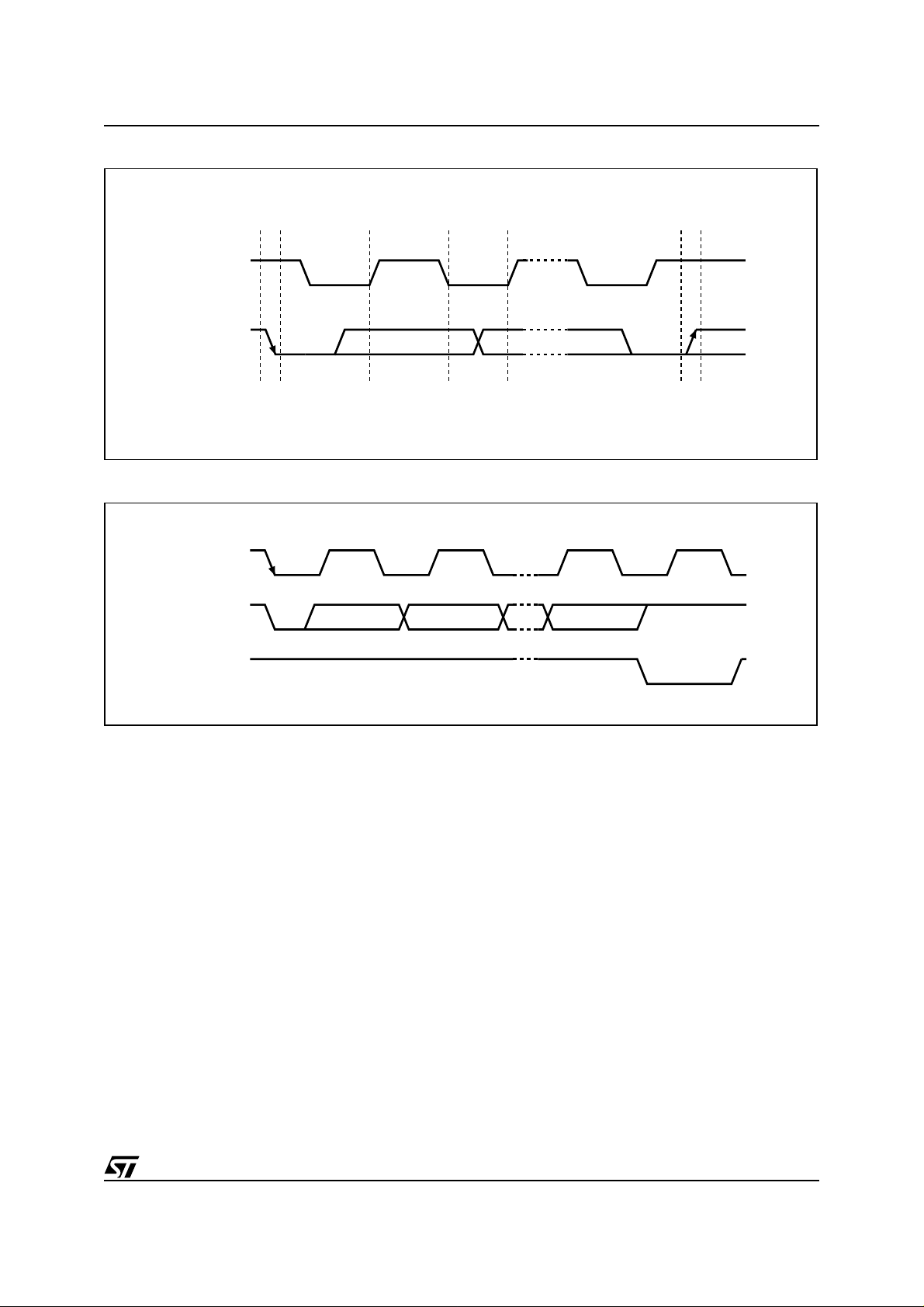
Figure 5. Serial Bus Data Transfer Sequence
DATA LINE
STABLE
DATA VALID
CLOCK
DATA
M41T00S
START
CONDITION
Figure 6. Acknowledgement Sequence
START
SCL FROM
MASTER
DATA OUTPUT
BY TRANSMITTER
DATA OUTPUT
BY RECEIVER
12 89
MSB LSB
CHANGE OF
DATA ALLOWED
STOP
CONDITION
AI00587
CLOCK PULSE FOR
ACKNOWLEDGEMENT
AI00601
7/23

M41T00S
READ Mode
In this mode the master reads the M41T00S slave
after setting the slave address (see Figure
8., page 9). Following the WRITE Mode Control
Bit (R/W
address 'An' is written to the on-chip address
pointer. Next the START condition and slave address are repeated followed by the READ Mode
Control Bit (R/W
mitter becomes the master receiver. The data byte
which was addressed will be transmitted and the
master receiver will send an A cknowledge Bit to
the slave transmitter. The address pointe r is only
incremented on reception of an Acknowledge
Clock. The M41T00S slave transmitter will now
place the data byte at address An+1 o n the bus,
the master receiver reads and acknowledges the
new byte and the address pointer is increm ented
to “An+2.”
Figure 7. Slave Address Location
=0) and the Acknowledge Bit, the word
=1). At this point the master trans-
This cycle of reading con secutive addresses will
continue until the master rec eiver sends a STOP
condition to the slave transmitter.
The system-to-user transfer of clock data will be
halted whenever the address being read is a clock
address (00h to 06h). The update will resu me due
to a Stop Condition or when the pointer increments
to any non-clock address (07h).
Note: This is true both in READ Mode and WRITE
Mode.
An alternate READ Mode may also be implemented whereby the mast er reads the M41T00S slave
without first writing to the (volatile) a ddress poin ter. The first address that is read is the last one
stored in the pointer (see Figure 9., page 9).
R/W
START A
SLAVE ADDRESS
MSB
0100011
LSB
AI00602
8/23

Figure 8. READ Mode Sequence
M41T00S
BUS ACTIVITY:
MASTER
SDA LINE
BUS ACTIVITY:
START
S
SLAVE
ADDRESS
R/W
ADDRESS (An)
ACK
DATA n+X
WORD
STOP
P
NO ACK
Figure 9. Alternative READ Mode Sequence
BUS ACTIVITY:
MASTER
START
R/W
START
S
ACK
ADDRESS
SLAVE
R/W
DATA n DATA n+1
ACK
ACK
ACK
AI00899
STOP
BUS ACTIVITY:
S
SLAVE
ADDRESS
DATA n DATA n+1 DATA n+X
ACK
ACK
ACK
ACK
PSDA LINE
NO ACK
AI00895
9/23

M41T00S
WRITE Mode
In this mode the master transmitter transmits to
the M41T00S slave receiver. Bus protocol is
shown in Figure 10. Following the START condi-
tion and slave address, a logic '0' (R/W
=0) is
placed on the bus and indicates to the addressed
device t ha t w or d address “ An” will follow and is t o
be written to the on-chip address pointer. The data
word to be written to the memory is strobed in next
and the internal address pointer is incremented to
the next address location on the reception of an
acknowledge clock. The M41T00S slave receiver
will send an acknowledge clock to the master
transmitter after it has received the s la ve addres s
see Figure 7., page 8 and again after it has received the word address and each data byte.
Figure 10. WR I TE Mode Sequence
BUS ACTIVITY:
MASTER
BUS ACTIVITY:
START
S
R/W
WORD
ADDRESS (An)
ACK
Data Retention Mode
With valid V
applied, the M41T00S can be ac-
CC
cessed as described above with REA D or WRI TE
Cycles. Should the supply voltage decay, the power input will be switched from the V
battery when V
Switchover Voltage (V
falls below the Battery Back-up
CC
). At this time the clock
SO
pin to the
CC
registers will be mainta ined by the attached battery supply. On power-up, when V
returns to a
CC
nominal value, write protection continues for t
For a further, more detailed review of lifetime cal-
culations, please see Application Note AN1012.
DATA n DATA n+1 DATA n+X
ACK
ACK
ACK
PSDA LINE
ACK
REC
STOP
.
SLAVE
ADDRESS
AI00591
10/23

CLOCK OPERATION
The 8-byte Register Map (see Table 2) is used t o
both set the clock and to read the date and time
from the clock, in a binary coded decimal form at.
Seconds, Minutes, and Hours are contained within
the first three registers.
Bits D6 and D7 of Clock Register 02h (Century/
Hours Register) contain the CENTURY ENABLE
Bit (CEB) and the CENTURY Bit (CB). Setting
CEB to a '1' will cause CB to toggle, either from '0'
to '1' or from '1' to '0' at the turn of the century (depending upon its initial state). If CEB is set to a '0,'
CB will not toggle. Bits D0 through D2 of Regi ster
03h contain the Day (day of week). Registers 04h,
05h, and 06h contain the Date (day of month),
Month and Years. The eighth clock register is the
Calibration Register (this is described in the Clock
Calibration section). Bit D7 of Register 00h contains the S TOP Bit (ST). Setting this bit to a ' 1 ' wil l
cause the oscillator to stop. If the device is expected to spend a significant amount of time on the
shelf, the oscillator may be stopped to reduce current drain. When reset to a '0' the oscillator restarts
within one second.
The seven Clock Registers may be read one by t e
at a time, or in a sequential block. The Calibration
Register (Address location 07h) may be accessed
M41T00S
independently. Provision has been made to assure that a clock update does not occur while any
of the seven clock addresses are being read. If a
clock address is being read, an update of the clock
registers will be halted. This will prevent a transition of data during the READ.
Clock Registers
The M41T00S offers 8 internal registers which
contain Clock and Calibration data. These registers are memory locations which contain external
(user accessible) and internal copies of the data
(usually referred to as BiPORT
cells). The external copies are independent of internal functions except that they are updated periodically by the simultaneous transfer of the
incremented internal copy. The internal divider (or
clock) chain will be reset upon the completion of a
WRITE to any clock address.
The system-to-user transfer of clock data will be
halted whenever the address being read is a clock
address (00h to 06h). The update will resum e either due to a Stop Condition or when the pointer
increments to any non-clock address (07h).
Clock Registers store data in BCD. The Calibration Register stores data in Binary Format.
™
TIMEKEEPER
®
Table 2. TIMEKEEPER
Addr
D7 D6 D5 D4 D3 D2 D1 D0
00h ST 10 Seconds Seconds Seconds 00-59
01h OF 10 Minutes Minutes Minutes 00-59
02h CEB CB 10 Hours Hours (24 Hour Format)
03h00000 Day of Week Day01-7
04h 0 0 10 Date Date: Day of Month Date 01-31
05h 0 0 0 10M Month Month 01-12
06h 10 Years Year Year 00-99
07h OUT FT S Calibration Calibration
Keys: 0 = Must be set to '0'
CB = Centur y B i t
CEB = Centur y E nable Bit
FT = Frequency Test Bit
Register Map
OF = Oscillator Fail Bit
OUT = Output level
S = Sign Bit
ST = Stop Bit
Function/Range BCD
Format
Century/
Hours
0-1/00-23
11/23

M41T00S
Calibrating the C lock
The M41T00S is driven by a quart z-co ntrolled oscillator with a nominal frequency of 32,768 Hz. The
devices are tested not exceed ±35 ppm (parts per
million) oscil lator frequency error at 25
equates to about ±1.53 mi nutes per month (see
Figure 11., page 13). Wh en the Calibration circuit
is properly employed, accuracy improves to better
than ±2 ppm at 25°C.
The oscillation rate of crystals changes with temperature. The M41T 00S design emp loys periodic
counter correction. The calibration circuit adds or
subtracts counts from t he oscillator divider circuit
at the divide by 256 stage, as shown in Figure
12., page 13. The numbe r of times pulses which
are blanked (subtracted, negative calibration) or
split (added, positive calibration) depends upon
the value loaded into the five Calibration Bits found
in the Calibration Register. Adding count s speeds
the clock up, subtracting cou nts slows the clock
down.
The Calibration Bits occupy the five lower order
bits (D4-D0) in the Calibration Register 07h. These
bits can be set to represent any value between 0
and 31 in binary form. Bit D5 is a Sign Bit; '1' indicates positive calibration, '0' indicates negative
calibration. Calibration occurs within a 64 m inute
cycle. The first 62 m inut es i n t he c ycle m ay , once
per minute, have one second either shortened by
128 or lengthened by 256 oscillator cycles. If a binary '1' is loaded into the register, only the first 2
minutes in the 64 minute cycle will be modified; if
a binary 6 is loaded, the first 12 will be affected,
and so on.
Therefore, each calibration step has t he effect of
adding 512 or subtracting 256 oscillator cycles for
every 125,829,120 actual oscillator cycles, that is
+4.068 or –2.034 ppm of adjustment per calibration step in the calibration register (see Figure
12., page 13). Assuming that the os cillator is run-
o
C, which
ning at exactly 3 2,768 Hz, each of the 31 increments in the Calibration byte would represent
+10.7 or –5.35 s econds per month which corresponds to a total range of +5.5 or –2.75 minu tes
per month.
Two methods are available for ascertaining how
much calibration a given M41T00S may require.
The first involves setting the clock, letting it run for
a month and comparing it to a known accurate reference and recording deviation over a fixed period
of time. Calibration values, including the number of
seconds lost or gained in a given period, can be
found in Application Note AN934, “TIMEKEEP-
®
CALIBRATION.” This allows the designer to
ER
give the end user the ability to calibrate the clock
as the environment requires, even if the final product is packaged in a non-user serviceable enclosure. The designer could provide a simple utility
that accesses the Calibration byte.
The second approach is better suited t o a manufacturing environment, and involves the use of the
FT/OUT pin. The pin will toggle at 512Hz, when
the Stop Bit (ST, D7 of 00h) is '0,' and the Frequency Test Bit (FT, D6 of 07h) is '1.'
Any deviation from 512 Hz indicates the degree
and direction of oscillator frequency shift at the test
temperature. For example, a reading of
512.010124 Hz would indicate a +20 ppm oscillator frequency error, requiring a –10 (XX001010) to
be loaded into the Calibration Byte for correction.
Note that setting or changing the Calibration Byte
does not affect the Frequency Test output frequency.
The FT/OUT pin is an open drain output which requires a pull-up resistor to V
for proper opera-
CC
tion. A 500-10k resistor is recommended in order
to control the rise time. The FT Bit is cleared on
power-down.
12/23

Figure 11. Crystal Accuracy Across Temp eratur e
Frequency (ppm)
20
0
–20
–40
–60
F
∆
–80
–100
–120
–140
–160
0 10203040506070
F
K
Temperature °C
= K x (T – T
2
)
O
= –0.036 ppm/°C2 ± 0.006 ppm/°C
T
= 25°C ± 5°C
O
M41T00S
2
80–10–20–30–40
AI07888
Figure 12. Cl ock Ca l ib rat i on
NORMAL
POSITIVE
CALIBRATION
NEGATIVE
CALIBRATION
AI00594B
13/23

M41T00S
Century Bit
Bits D7 and D6 of Clock Register 02h contain the
CENTURY ENABLE Bit (CEB) and the CENTURY
Bit (CB). Setting CEB to a '1' will cause CB to toggle, either from a '0' to '1' or from '1' to '0' at the turn
of the century (depending upon its initial state). If
CEB is set to a '0,' CB will not toggle.
Oscillator Fail Detection
If the Oscillator Fail Bit (OF) is internally set to '1,'
this indicates that the oscillator has either stopped,
or was stopped for some period of time and can be
used to judge the validity of the clock and date data.
In the event the OF Bit is found to be set to '1' at
any time other than the initial power-up, the STOP
Bit (ST) should be written to a '1,' then immediately
reset to '0.' This w ill r es tart the oscillator.
The following conditions can cause the OF Bit to
be set:
– The first time power is applied (defaults to a '1'
on pow er-u p).
– The voltage present on V
suppo rt os c illation.
– The ST Bit is set to '1.'
– External interference of the crystal.
is insufficien t to
CC
The OF Bit will remain set to '1' until written to logic
'0.' The oscillator must start and have run for at
least 4 seconds before attempting to reset the OF
Bit to '0.'
Output Driver Pin
When the FT Bit is not set, the FT/OUT pi n becomes an output driver that reflects the contents of
D7 of the Calibration Register. In other words,
when D7 (OUT Bit) and D6 (FT Bit) of address location 07h are a '0,' then the F T/OUT pin will be
driven low.
Note: The FT/OUT pin is an open drain whic h requires an external pull-up resistor.
Preferred Initial Power-on Default
Upon initial application of power to the device, the
ST and FT bits are set to a '0' state, and the OF
and OUT Bits will be set to a '1.' All other Register
bits will initially power-on in a random state (see
Table 3).
Table 3. Preferred Default Values
Condition ST Out FT OF
Initial Power-up
Subsequent Power-up (with battery back-up)
Note: 1. State of other control bits undefined.
2. UC = Unchanged
(1)
(2)
0101
UC UC 0 UC
14/23

M41T00S
MAXIMUM RA T ING
Stressing the device above the rating l isted in t he
“Absolute Maximum Ratings” table may cause
permanent damage to the device. These are
stress ratings only and operation of the device at
these or any other conditions above those indicated in the Operating sections of this specification is
Table 4. Absolute Maximum Ratings
Sym Parameter Value Unit
T
V
T
V
P
Note: 1. For SO8 package, Lead-free (Pb-free) lead finish: Reflow at peak temperature of 260°C (total thermal budget not to exceed 245°C
Storage T emperature (VCC Off, Oscillator Off)
STG
Supply Voltage
CC
Lead Solder Temperature for 10 Seconds
SLD
Input or Output Voltages –0.3 to Vcc+0.3 V
IO
I
Output Current 20 mA
O
Power Dissipation 1 W
D
for greater than 30 seconds).
2. For SO8 package, standard (SnPb) lead finish: Reflow at peak temperature of 240°C (total thermal budget not to exceed 180°C for
between 90 to 150 seco nd s ) .
3. The SO X18 pac kage ha s Lead- free (P b-fr ee) l ead fin ish , b ut c an not b e exp os ed to peak r eflow tem perat ur e in ex c ess of 24 0°C
(use same re flow profile as standard (S nPb) lead finish).
CAUTION: Negative under shoots below –0.3 volts are not allowed on any pin while in t he Battery Back-up Mode
not implied. Exposure to Absol ute Max imum Ra ting conditions for extended periods may affect device reliability. Refer also to the
STMicroelectronics SURE Program and other relevant quality documents.
SOIC –55 to 125
Lead-free lead finish
Standard (SnPb)
lead finish
(2,3)
(1)
–0.3 to 7
260 °C
240 °C
°C
V
15/23

M41T00S
DC AND AC PARAMETERS
This section summarizes the operating and measurement conditions, as well as the DC and AC
characteristics of the device. The parameters in
the following DC and AC Characteristic tables are
derived from tests performed under the Meas ure-
Table 5. Operating and AC Measurement Conditions
Parameter M41T00S
ment Conditions listed in t he relevant tables. Designers should check that the operating conditions
in their projects match the measurement conditions when using the quoted parameters.
Supply Voltage (V
Ambient Operating Temperature (T
Load Capacitance (C
CC
)
)
A
)
L
2.7 to 5.5V
–40 to 85°C
100pF
Input Rise and Fall Times ≤ 50ns
0.2V
0.3V
to 0.8 V
CC
to 0.7 V
CC
Input Pulse Voltages
Input and Output Timing Ref. Voltages
Note: O utput Hi-Z is defined as the poi nt where data i s no longer dri ven.
Figure 13. AC Measureme nt I/ O Wa veform
0.8V
0.2V
CC
CC
0.7V
0.3V
AI02568
CC
CC
CC
CC
Table 6. Capacitance
Symbol
C
IN
(3)
C
OUT
t
LP
Note: 1. Effec tive capacit ance measured with power supply at 5V; sampled only, not 100 % t ested.
2. At 25°C, f = 1MHz.
3. Out puts deselect ed.
Input Capacitance 7 pF
Output Capacitance 10 pF
Low-pass filter input time constant (SDA and SCL) 50 ns
Parameter
16/23
(1,2)
Min Max Unit

Table 7. DC Characteristics
Sym Parameter
I
Input Leakage Current
LI
I
Output Leakage Current
LO
I
I
Supply Current Switch Freq = 400kHz 300 µA
CC1
Supply Current (standby)
CC2
Test Condition
0V ≤ V
0V ≤ V
IN
OUT
≤ V
≤ V
SCL = 0Hz
All Inputs
≥ VCC – 0.2V
≤ VSS + 0.2V
CC
(1)
CC
M41T00S
Min Typ Max Unit
±1 µA
±1 µA
70 µA
V
Input Low Voltage –0.3
IL
V
Input High Voltage
IH
I
Output Low Voltage
V
OL
Output Low Voltage (Open Drain)
(2)
= 3.0mA
OL
IOL = 10mA
0.7V
CC
0.3V
CC
VCC + 0.3
0.4 V
0.4 V
V
V
Pull-up Supply Voltage (Open Drain) FT/OUT 5.5 V
(3)
V
BA T
I
Note: 1. Valid for Ambient Operating Tem perature : TA = –40 to 85°C; VCC = 2.7 to 5. 5V (except wh ere noted).
Back-up Supply Voltage 2.0
T
= 25°C, VCC = 0V
Battery Supply Current
BAT
2. For F T/OUT pin (Open Drain)
3. STMi croelectronics recommends the R AY OVAC BR12 25 or BR1632 (or equivalen t) as t he battery supply.
4. For rechargea bl e back-up, V
(max) may be considere d to be VCC.
BAT
A
Oscillator ON, V
BA T
= 3V
0.6 1 µA
3.5
(4)
V
Table 8. Crystal Electrical Characteristics
Sym
f
O
R
S
C
L
Note: 1. Extern ally supp li ed i f us ing th e S O8 pa ckag e. STM icroe lec troni cs reco mm ends the K DS DT -38: 1TA/ 1TC 252 E127 , Tun ing Fork
Type (thru-hole) or the DMX-26S: 1TJS125FH2A212, (SMD) quartz crystal for industrial temperature operations. KDS can be contacted at kouhou@kdsj .c o. j p or http://ww w. kdsj.co.j p f or further info rmation on this crystal type.
2. Load capacitors are integrated within the M41T00S. Circuit board layout considerations for the 32.768kHz crystal of minimum trace
lengths and i solation from RF generating signals should be taken i nto account.
3. For applicati ons requiring back-up su ppl y operation bel ow 2.5V, R
Resonant Frequency 32.768 kHz
Series Resistance
Load Capacitance 12.5 pF
Parameter
(1,2)
(max) should be considered 40kΩ.
S
Min Typ Max Units
60
(3)
kΩ
17/23

M41T00S
Figure 14. Power Down/Up Mode AC Waveforms
V
CC
VSO
SDA
SCL
Table 9. Power Down/Up AC Characteristics
Symbol
t
PD
t
rec
Note: 1. VCC fall time should not exceed 5mV/µs.
2. Va li d for Ambient Operating Temperature : T
Table 10. Power Down/Up Trip Points DC Characteristics
Sym
V
Power-fail Deselect 2.5 2.6 2.7 V
PFD
Hysteresis 25 mV
tPD
DON'T CARE
Parameter
(1,2)
SCL and SDA at VIH before Power Down
SCL and SDA at VIH after Power Up
= –40 to 85°C; VCC = 2.7 to 5. 5V (except wh ere noted).
A
Parameter
(1,2)
trec
AI00596
Min Typ Max Unit
0nS
10 µS
Min Typ Max Unit
Battery Back-up Switchover Voltage
< V
(V
V
SO
CC
; VCC < V
BAT
PFD
Hysteresis 40 mV
Note: 1. All voltages referenced to VSS.
2. Va li d for Ambient Operating Temperature : T
< V
V
BA T
PFD
)
A
V
> V
BA T
PFD
= –40 to 85°C; VCC = 2.7 to 5. 5V (except wh ere noted).
V
BAT
V
PFD
V
V
18/23

Figure 15. Bus Timing Requirements Sequence
SDA
M41T00S
tHD:STA
SCL
tHD:STAtBUF
tHIGH
tLOW
tF
tSU:DAT
tHD:DAT
SR
tR
SP
Table 11. AC Characteristics
Sym
f
SCL
t
LOW
t
HIGH
t
R
t
F
t
HD:STA
t
SU:STA
t
SU:DAT
t
HD:DAT
t
SU:STO
t
BUF
Note: 1. Valid for Ambient Operating Tem perature : TA = –40 to 85°C; VCC = 2.7 to 5. 5V (except wh ere noted).
2. Transmitter must internal l y provide a hold time to brid ge t he undefined region (300ns max) of the fa lli ng edge of SCL.
SCL Clock Frequency 0 400 kHz
Clock Low Period 1.3 µs
Clock High Period 600 ns
SDA and SCL Rise Time 300 ns
SDA and SCL Fall Time 300 ns
START Condition Hold Time
(after this period the first clock pulse is generated)
START Condition Setup Time
(only relevant for a repeated start condition)
(2)
Data Setup Time 100 ns
Data Hold Time 0 µs
STOP Condition Setup Time 600 ns
Time the bus must be free before a new
transmission can start
Parameter
(1)
Min Typ Max Units
600 ns
600 ns
1.3 µs
tSU:STOtSU:STA
P
AI00589
19/23

M41T00S
PACKAG E MECHANICA L INFORMATIO N
Figure 16. SO8 – 8-lead Plastic Small Package Outline
h x 45˚
A2
A
C
B
e
ddd
D
8
E
H
1
Note: D rawing is not to scale.
LA1 α
SO-A
Table 12. SO8 – 8-lead Plastic Small Outline (150 mils body width), Package Mech. Data
Symb
Typ Min Max Typ Min Max
A 1.35 1.75 0.053 0.069
mm inches
A1 0.10 0.25 0.004 0.010
A2 1.10 1.65 0.043 0.065
B 0.33 0.51 0.013 0.020
C 0.19 0.25 0.007 0.010
D 4.80 5.00 0.189 0.197
E 3.80 4.00 0.150 0.157
e1.27– –0.050– –
H 5.80 6.20 0.228 0.244
h 0.25 0.50 0.010 0.020
L 0.40 0.90 0.016 0.035
α 0° 8° 0° 8°
N8 8
ddd 0.10 0.004
20/23

M41T00S
PART NUMBERING
Table 13. Ordering Information Scheme
Example: M41T 00S M 6 E
Device Type
M41T
Supply Voltage and Write Protect Voltage
00S = V
Package
M = SO8
Temperature Range
6 = –40°C to 85°C
= 2.7 to 5.5V
CC
Shipping Method
For SO8:
E = Lead-free Package (ECO PACK
F = Lead-free Package (ECO PACK
®
), Tubes
®
), Tape & Reel
For other options, or for more information on any aspect of this device, please contact the ST Sales Office
nearest you.
21/23
M41T00S
REVISION HISTORY
Table 14. Document Revision History
Date Version Revision Details
February 10, 2004 0.1 First Draft
20-Feb-04 0.2 Update characteristics (Table 9, 10, 5, 7, 13)
14-Apr-04 1.0
05-May-04 1.1 Update DC Characteristics (Table 7)
16-Jun-04 1.2 Added package shipping (Table 13)
13-Sep-04 2.0 Update Maximum ratings (Table 4)
26-Nov-04 3.0
M41T00S, 41T00S, T00S, Serial, Serial, Serial, Serial, Serial, Serial, Serial, Serial, Serial, Serial, Serial, Serial, Serial, Serial, Serial, Serial, Serial, Serial, Serial, Serial,
Serial, Serial, Serial, Serial, Serial, Serial, Serial, Serial, Serial, Serial , Seri al, Seria l, Seria l, Serial , Seri al, Se rial, Serial, Serial, Serial, Serial, Serial, Serial, Serial, Serial,
Serial, Access, Access, Access, Access, Access, Access, Access, Access, Access, Access, Access, Access, Access, Access, Access, Access, Access, Access, Access,
Access, Access, Access, Access, Access, Access, Access, Access, Access, Access, Access, Access, Access, Access, Access, Access, Access, Access, Access, Access, Access, Access, Access, Access, Access, Access, Access, Access, Access, Access, Access, Access, A ccess, Access, Access, Access, Access, Access, Access,
Access, Access, Access, Access, Access, Access, Access, Access, Access, Access, Access, Access, Access, Access, Access, Access, Access, Interface, Interface,
Interface, Inter face , In terfa c e, Inte rfa ce, Inte rface, Inte r face , Int erface , In ter fa ce, In terfa c e, Inte rfa ce, Inte rface, Inte r face , Int erface , In ter fa ce, In terfa c e, Inte rfa ce, Inte rface, Interfac e, Inter face , In ter fa ce, I nte rface , In ter fa ce, I nte rfac e, Int erface , In te rfac e, Int erface , In ter fa ce, I nte rface , In ter fa ce, I nte rf ace , Int erfa ce, In te rfac e, Int erface ,
Interface, Inter face , In terfa c e, Inte rfa ce, Inte rface, Inte r face , Int erface , In ter fa ce, In terfa c e, Inte rfa ce, Inte rface, Inte r face , Int erface , In ter fa ce, In terfa c e, Inte rfa ce, Inte rface, Interfac e, Inter face , In ter fa ce, I nte rface , In ter fa ce, I nte rfac e, Int erface , In te rfac e, Int erface , In ter fa ce, I nte rface , In ter fa ce, I nte rf ace , Int erfa ce, In te rfac e, Int erface ,
Interface, Inter face , In terfa c e, Inte rfa ce, Inte rface, Inte r face , Int erface , In ter fa ce, In terfa c e, Inte rfa ce, Inte rface, Inte r face , Int erface , In ter fa ce, In terfa c e, Inte rfa ce, Inte rface, Interface, Interface, Interface, Interface, Interface, Clock, Clock, Clock, Clock, Clock, Clock, Clock, Clock, Clock, Clock, Clock, Clock, Clock, Clock, Clock, Clock,
Clock, Clock, Clock, Clock, Clock, Clock, Clock, Clock, Clock, Clock, Clock, Clock, Clock, Clock, Clock, Clock, Clock, Clock, Clock, Clock, Clock, Clock, Clock, Clock,
Clock, Clock, Clock, Clock, Clock, Clock, Clock, Clock, Clock, Clock, Clock, Clock, Clock, Clock, Clock, Clock, Clock, Clock, Clock, Clock, Clock, Clock, Clock, Clock,
Clock, Clock, Clock, Clock, Clock, Clock, Clock, Clock, Clock, Clock, Clock, Clock, Clock, Clock, Clock, Clock, Clock, Clock, Clock, Clock, Clock, Clock, Clock, Clock,
Clock, Clock, Clock, Clock, Clock, Clock, Clock, Clock, Clock, Clock, Clock, Clock, Clock, Clock, Clock, Clock, Clock, Clock, Clock, Clock , Clock, Clo ck, R TC, RTC, RTC,
RTC, RTC, RTC, RTC, RTC, RTC, RTC, RTC, RTC, RTC, RTC, RTC, RTC, RTC, RTC, RTC, RTC, RTC, RTC, RTC, RTC, RTC, RTC, RTC, RTC, RTC, RTC, RTC,
RTC, RTC, RTC, RTC, RTC, RTC, RTC, RTC, RTC, RTC, RTC, RTC, RTC, RTC, RTC, RTC, RTC, RTC, RTC, RTC, RTC, RTC, RTC, RTC, RTC, RTC, RTC, RTC,
RTC, RTC, RTC, RT C, RTC, RTC, Pro gramm able , Progr am mable, Prog ramma ble, Pr ogra mmab le, P rogra mmab le, Pro gram ma ble, Pr ogra mmabl e, Programmable, Programmable, Programmable, Programmable, Programmable, Programmable, Programmable, Programmable, Programmable, Programmable, Programm ab le, Programmable , P rog ra mm ab le, Pr og ra mma b le, Pr og r am ma bl e, Pro g ram ma ble , Pro gr am ma ble , Pro gr am mab le , Pr ogr am m abl e, P rog ra mm ab le, Pr og ra mmable, Programmable,
Progra mmab le, Pr ogra mmab le, Pr ogra mmabl e, Pro gramm abl e, Prog ramm able, Prog ramma ble, P rogra mma ble, Pr ogra mma ble, Progra mmabl e, Prog ram mable, Pr ogrammable, Programmable, Programmable, Programmable, Programmable, Programmable, Programmable, Programmable, Programmable, Programm ab le, Programmable, Programmable, Programmable, Programmable, Programmable, Programmable, Programmable Alarm, Programmable Alarm, Programmable Alarm,
Programmable Alarm, Programmable Alarm, Programmable Alarm, Programmable Alarm, Programmable Alarm, Programmable Alarm, Programmable Alarm, Alarm,
Alarm, Alarm, Alarm, Alarm, Alarm, Alarm, Alarm, Alarm, Alarm, Alarm, Alarm, Alarm, Alarm, Alarm, Alarm, Alarm, Alarm, Alarm, Alarm, Alarm, Alarm, Alarm, Alarm,
Alarm, Alarm, Alarm, Alarm, Alarm, Alarm, Alarm, Alarm, Alarm, Alarm, Alarm, Alarm, Alarm, Alarm, Alarm, Alarm, Alarm, Alarm, Alarm, Alarm, Alarm, Alarm, Alarm,
Alarm, Alarm, Alarm, Alarm, Alarm, Alarm, Alarm, Alarm, Alarm, Alarm, Alarm, Alarm, Alarm, Alarm, Alarm, Alarm, Alarm, Alarm, Alarm, Alarm, Alarm, Alarm, Alarm,
Alarm, Alarm, Alarm, Alarm, Alarm, Alarm, Alarm, Alarm, Alarm, Alarm, Alarm, Alarm, Alarm, Alarm, Alarm, Alarm, Alarm, Alarm, Alarm, Alarm, Alarm, Alarm, Alarm,
Alarm, Alarm , Ala rm , A larm, Alarm, Alarm, Al arm , In ter rupt , In ter r upt, In ter r upt, In te rr upt, Interrupt, I nterr u pt, Inter ru pt, Int erru pt, Int erru pt , In terru pt , In terr upt, In ter r upt,
Interrupt, Interrupt, Interrupt, Interrupt, Interrupt, Interrupt, Interrupt, Interrupt, Interrupt, Interrupt, Interrupt, Interrupt, Interrupt, Interrupt, Interrupt, Interrupt, Interrupt, Interrupt, Interrupt, Interrupt, Interrupt, Interrupt, Interrupt, Interrupt, Interrupt, Interrupt, Interrupt, Interrupt, Interrupt, Interrupt, Interrupt, Interrupt, Interrupt, Interrupt, Interrupt, Interrupt, Interrupt, Interrupt, Interrupt, Interrupt, Interrupt, Interrupt, Interrupt, Interrupt, Interrupt, Interrupt, Interrupt, Interrupt, Interrupt, Interrupt, Interrupt, Interrupt,
Interrupt, Interrupt, Interrupt, Interrupt, Interrupt, Interrupt, Interrupt, Interrupt, Interrupt, Interrupt, Interrupt, Interrupt, Interrupt, Interrupt, Interrupt, Interrupt, Interrupt, Interrupt, Interrupt, Interrupt, Interrupt, Interrupt, Interrupt, Interrupt, Interrupt, Interrupt, Interrupt, Interrupt, Interrupt, Interrupt, Interrupt, Interrupt, Interrupt, Interrupt, Interrupt, Interrupt, Interrupt, Interrupt, Interrupt, Interrupt, Interrupt, Interrupt, Interrupt, Interrupt, Interrupt, Interrupt, Interrupt, Interrupt, Interrupt, Interrupt, Interrupt, Interrupt,
Interrupt, Interrupt, Interrupt, Interrupt, Interrupt, Interrupt, Interrupt, Interrupt, Interrupt, Interrupt, Interrupt, Interrupt, Interrupt, Interrupt, Interrupt, Interrupt, Interrupt, Interrupt, Interrupt, Interrupt, Interrupt, Interrupt, Interrupt, Interrupt, Interrupt, Interrupt, Interrupt, Interrupt, Interrupt, Interrupt, Interrupt, Interrupt, Interrupt, Interrupt, Interrupt, Interrupt, Interrupt, Interrupt, Interrupt, Interrupt, Interrupt, Interrupt, Interrupt, Interrupt, Interrupt, Interrupt, Interrupt, Interrupt, Interrupt, Interrupt, Interrupt, Interrupt,
Interrupt, Interrupt, Interrupt, Interrupt, Interrupt, Interrupt, Interrupt, Interrupt, Interrupt, Interrupt, Interrupt, Interrupt, Watchdog, Watchdog, Watchdog, Watchdog, Watchdog, Wat chd og, Wa tch do g, Wat chd og, Wa tch dog , Wat chd og, Watc hdog , Wat chd og, Watc hdog , Wat chdo g, Watc hdog , Wat chdo g, Watc hdog , Wa tc hdog, Wat chdog ,
Watchdog, Watchdog, Watchdog, Watchdog, Watchdog, Watchdog, Watchdog, Watchdog, Watchdog, Watchdog, Watchdog, Watchdog, Watchdog, Watchdog, Watchdog, Wat chd og, Wa tch do g, Wat chd og, Wa tch dog , Wat chd og, Watc hdog , Wat chd og, Watc hdog , Wat chdo g, Watc hdog , Wat chdo g, Watc hdog , Wa tc hdog, Wat chdog ,
Watchdog, Watchdog, Batter y, B att er y, B atte r y, Ba tte ry, Battery, Bat tery , B att ery , B atte r y, Ba tte ry, Ba tte ry, Bat ter y, B attery, Batt ery , Ba tte ry, Ba tte ry, Bat ter y, Battery,
Battery, Battery, Battery, Battery, Battery, Battery, Battery, Battery, Battery, Battery, Battery, Battery, Battery, Battery, Battery, Battery, Battery, Battery, Battery, Battery,
Battery, Battery, Battery, Battery, Battery, Battery, Battery, Battery, Battery, Battery, Battery, Battery, Battery, Battery, Battery, Battery, Battery, Battery, Battery, Battery,
Battery, Battery, Battery, Switchover, Switchover, Switchover, Switchover, Switchover, Switchover, Switchover, Switchover, Switchover, Backup, Backup, Backup, Backup, Backup, Backup, Backup, Backup, Backup, Backup, Backup, Backup, Backup, Backup, Backup, Backup, Backup, Backup, Backup, Backup, Write Pr otect , Wr ite
Protect, W rit e Pr ot ec t, Write P ro tec t, Write Pr ote c t, W r it e Pr ot ec t, Write P ro tect, Writ e Pr ote c t, W r it e Pr o tec t, Write P ro tect, Write Protect, Write Protect, Write Protect,
Write Protect, Write Protect, Write Protect, Write Protect, Write Protect, Write Protect, Write Protect, Write Protect, Write Protect, Write Protect, Write Protect, Write Protect, Industrial , Industrial , Industria l, Industr ial, Industr ial, In dustrial, Industri al, Industri al, Indu strial, Indu strial, Ind ustrial, v Industria l, Indus trial, Ind ustrial, SOI C, SOIC,
SOIC, SOIC, SOIC, SOIC, SOIC, SOIC, SOIC , SOIC , SOIC, SOIC , SOIC, SOIC , SOIC
Product promoted; reformatted; update characteristics, including Lead-free package
information (Figure 4. 11; Table 4. 11, 13)
Promote document; update characteristics; remove references to SOX18 package
(Figure 1, 5; Table 14)
22/23

M41T00S
Information furnished is believed to be accurate and reliable. However, STMicroelectronics a ssumes no responsibility fo r the c onsequences
of use of such information nor for any infringement of patents or other rights of third parties which may result from its use. No license is granted
by implication or otherwise under any patent or patent rights of STMicroelectronics. Specifications mentioned in this publication are subject
to change without notice. This publication supersedes and replaces all information previously supplied. STMicroelectronics products are not
authori zed for use as crit i cal components in life support devices or systems w i th out express written app rov al of STMicroel ectronics.
The ST logo is a registered trademark of STM i croelectronics.
All other nam es are the property of their respective owners
© 2004 STMi croelectro ni cs - All rights reserved
Australi a - Belgium - B raz i l - Canada - Ch i na - Czech Rep ubl i c - Finland - France - Germany - Hong Ko ng - I n dia - Israel - It al y - Japan -
Malaysia - M al ta - Morocco - Singapore - Spain - Sweden - Switzerl and - United K i ngdom - Unite d States of Am eri ca
STMicroelectronics group of com panies
www.st.com
23/23
 Loading...