

Sony XM-754SX Service manual
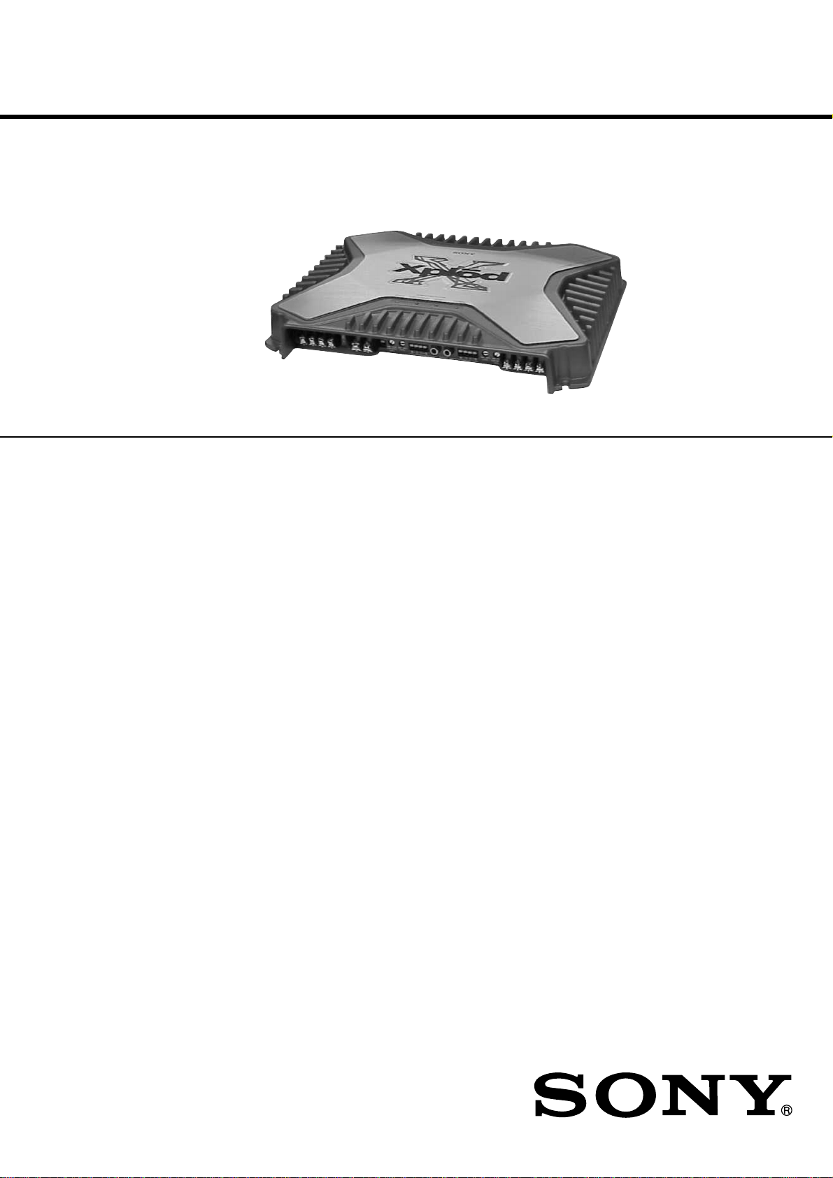
XM-754SX
SERVICE MANUAL
Ver 1.1 2001. 05
SPECIFICATIONS
AUDIO POWER SPECIFICATIONS (US MODEL)
POWER OUTPUT AND TOTAL HARMONIC DISTORTION
75 watts per channel minimum continuous average power into
4 ohms, both channels driven from 20 Hz to 20 kHz with no more
than 0.04% total harmonic distortion per Car Audio Ad Hoc
Committee standards.
US Model
Canadian Model
AEP Model
UK Model
E Model
Other Specifications
Circuit system OTL (output transformerless) circuit
Inputs RCA pin jacks
Outputs Speaker terminals
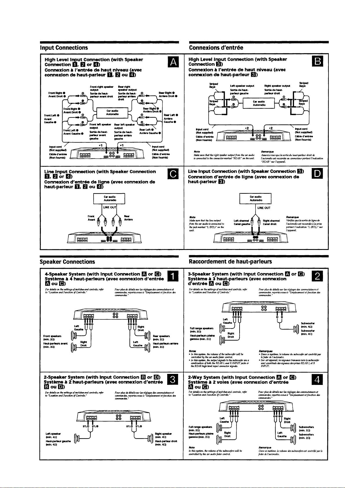
Speaker impedance 2 – 8 Ω (stereo)
Maximum outputs Four speakers: 170 W × 4 (at 4 Ω)
Rated outputs (supply voltage at 14.4 V)
Frequency response 5 Hz – 100 kHz ( dB)
Harmonic distortion 0.005% or less (at 1 kHz, 4 Ω)
Pulse power supply
High level input connector
4 – 8 Ω (when used as a bridging amplifier)
Three speakers: 170 W × 2 + 400 W × 1 (at 4 Ω)
Two speakers: 400 W × 2 (at 4 Ω)
Four speakers:
75 W × 4 (20 Hz – 20 kHz, 0.04% THD, at 4 Ω)
100 W × 4 (20 Hz – 20 kHz, 0.1% THD, at 2 Ω)
Two speakers:
200 W × 2 (20 Hz – 20 kHz, 0.1% THD, at 4 Ω)
+0.5
–3
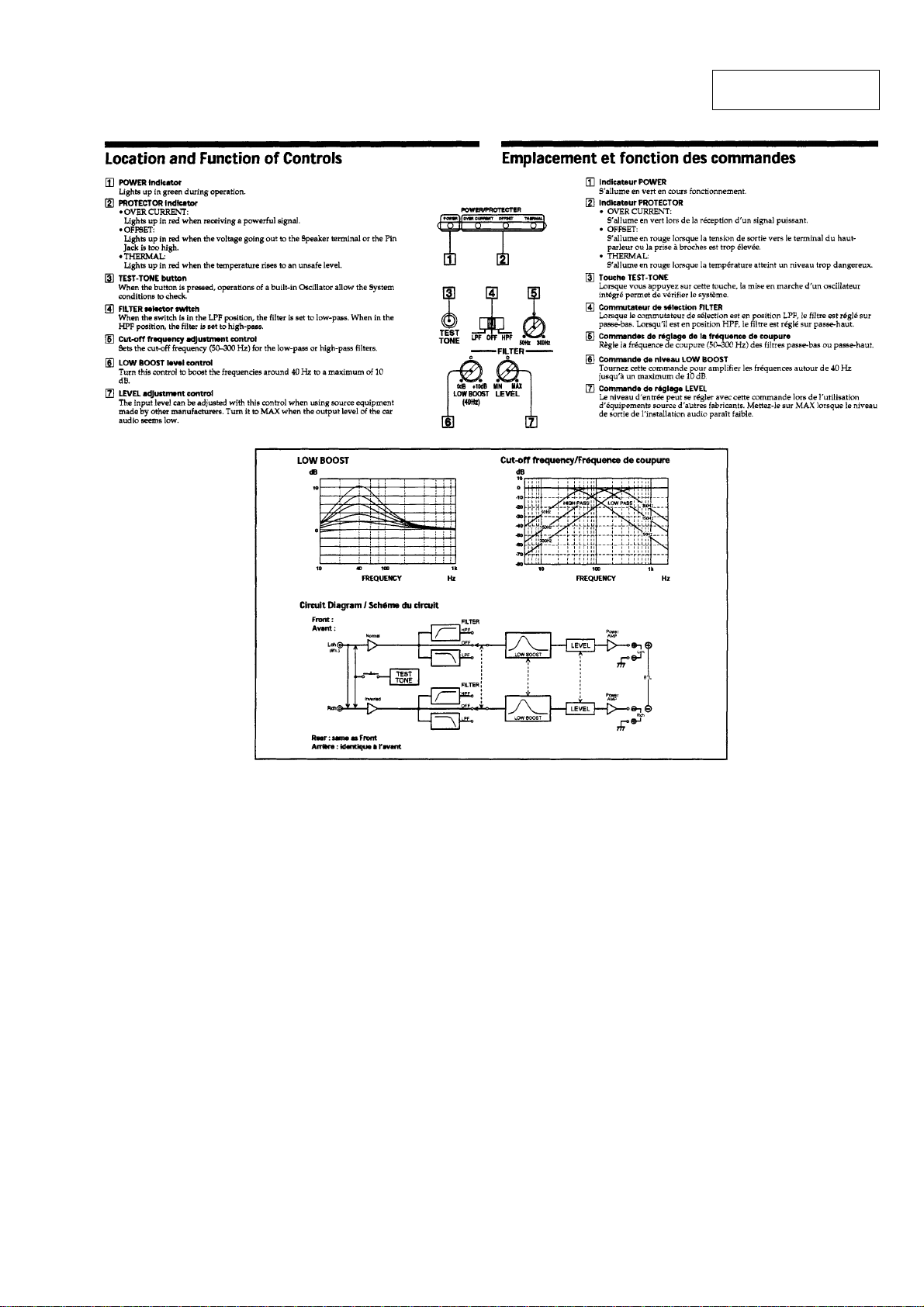
Input level adjustment range
High-pass filter 50 – 300 Hz, –12 dB/oct
Low-pass filter 50 – 300 Hz, –12 dB/oct
Low boost 0 – 10 dB (40 Hz)
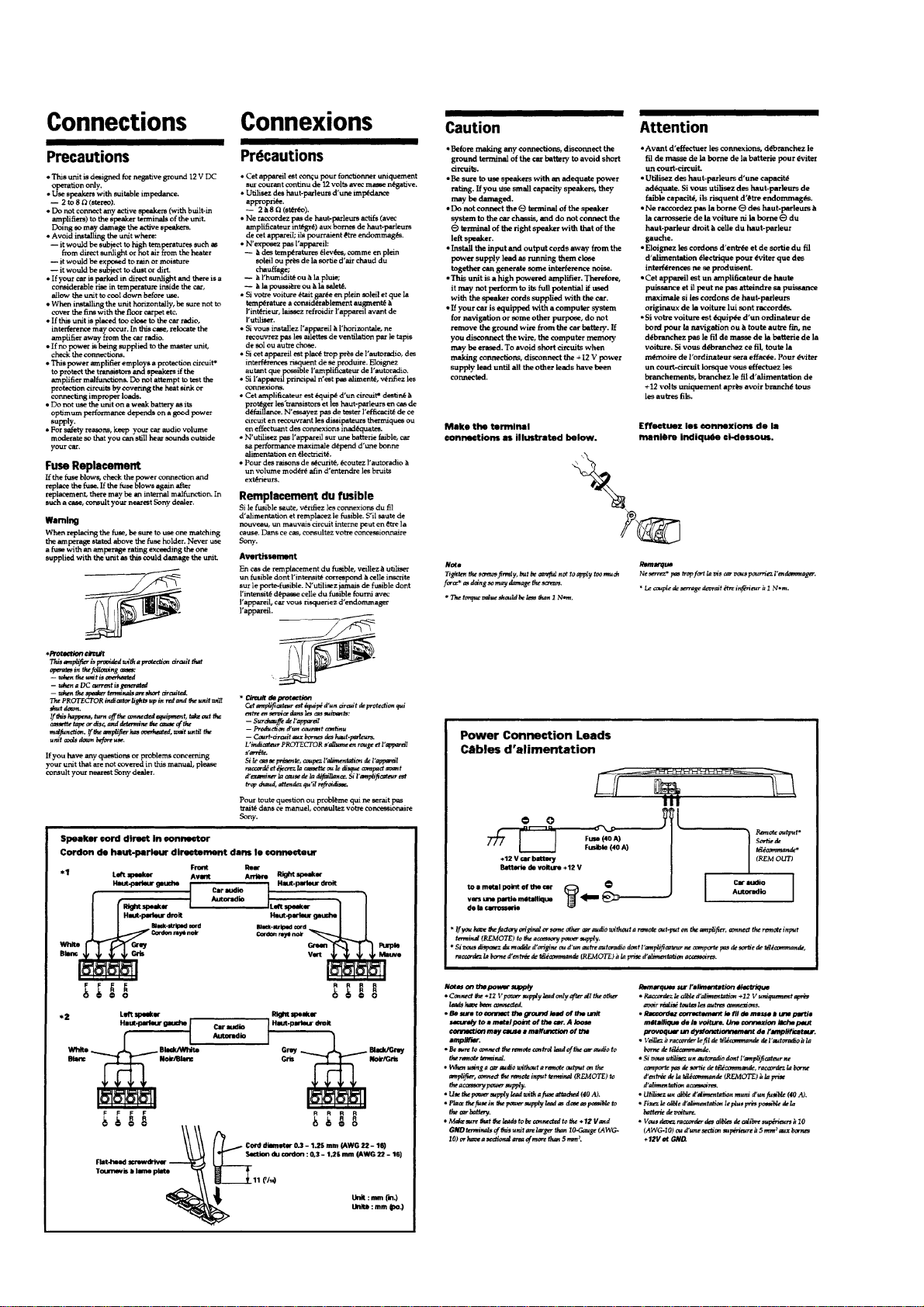
Power requirements 12 V DC car battery
Power supply voltage 10.5 – 16 V
Current drain at rated output : 40 A (4 Ω)
Dimensions Approx. 358 × 50 × 264 mm
Mass Approx. 3.5 kg (7 lb. 11 oz.) not incl. accessories
Supplied accessories Mounting screws (4)
Design and specifications are subject to change without
notice.
Notes on Chip Component Replacement
• Never reuse a disconnected chip component.
• Notice that the minus side of a tantalum capacitor may be
damaged by heat.
0.2 – 6.0 V (RCA pin jacks)
0.4 – 12.0 V (High level input)
(negative ground)
Remote input : 1.5 mA
(w/h/d) (14
projecting parts and controls
1/8 × 2 × 10 1/2 in.) not incl.
9-873-503-11
2001E0400-1
© 2001. 5
STEREO POWER AMPLIFIER
Sony Corporation
e Vehicle Company
Shinagawa Tec Service Manual Production Group
1

XM-754SX
TABLE OF CONTENTS
1. GENERAL
Location and Function of Controls.......................................... 3
Connections ............................................................................. 4
2. DISASSEMBLY
2-1. Plate, Bottom ....................................................................... 6
2-2. Main Board Section ............................................................. 6
2-3. Main Board, Filter (F) Board, Filter (R) Board ...................7
2-4. LED Board........................................................................... 7
3. ELECTRICAL ADJUSTMENT...................................... 8
4. DIAGRAMS
4-1. Block Diagram..................................................................... 9
4-2. Printed Wiring Board –Main Section– .............................. 11
4-3. Schematic Diagram –Main Section (1/2)– ........................ 12
4-4. Schematic Diagram –Main Section (2/2)– ........................ 13
4-5. Schematic Diagram –Filter (F), Filter (R),
LED Section– .................................................................... 14
4-6. Printed Wiring Boards –Filter (F), Filter (R),
LED Section– .................................................................... 15
5. EXPLODED VIEWS
5-1. Heat Sink (Main) Section .................................................. 17
5-2. Main Board Section ........................................................... 18
6. ELECTRICAL PARTS LIST ........................................ 19
SAFETY-RELATED COMPONENT WARNING!!
COMPONENTS IDENTIFIED BY MARK 0 OR DOTTED LINE
WITH MARK 0 ON THE SCHEMATIC DIAGRAMS AND IN
THE PARTS LIST ARE CRITICAL TO SAFE OPERATION.
REPLACE THESE COMPONENTS WITH SONY P ARTS WHOSE
PART NUMBERS APPEAR AS SHOWN IN THIS MANUAL OR
IN SUPPLEMENTS PUBLISHED BY SONY.
ATTENTION AU COMPOSANT AYANT RAPPORT
LES COMPOSANTS IDENTIFIÉS P AR UNE MARQUE 0 SUR LES
DIAGRAMMES SCHÉMATIQUES ET LA LISTE DES PIÈCES
SONT CRITIQUES POUR LA SÉCURITÉ DE FONCTIONNEMENT.
NE REMPLACER CES COMPOSANTS QUE PAR DES PIÈCES
SONY DONT LES NUMÉROS SONT DONNÉS DANS CE MANUEL
OU DANS LES SUPPLÉMENTS PUBLIÉS PAR SONY.
À LA SÉCURITÉ!!
2
SECTION 1
GENERAL
XM-754SX
This section is extracted
from instruction manual.
3
XM-754SX
4
XM-754SX
5
XM-754SX
g
SECTION 2
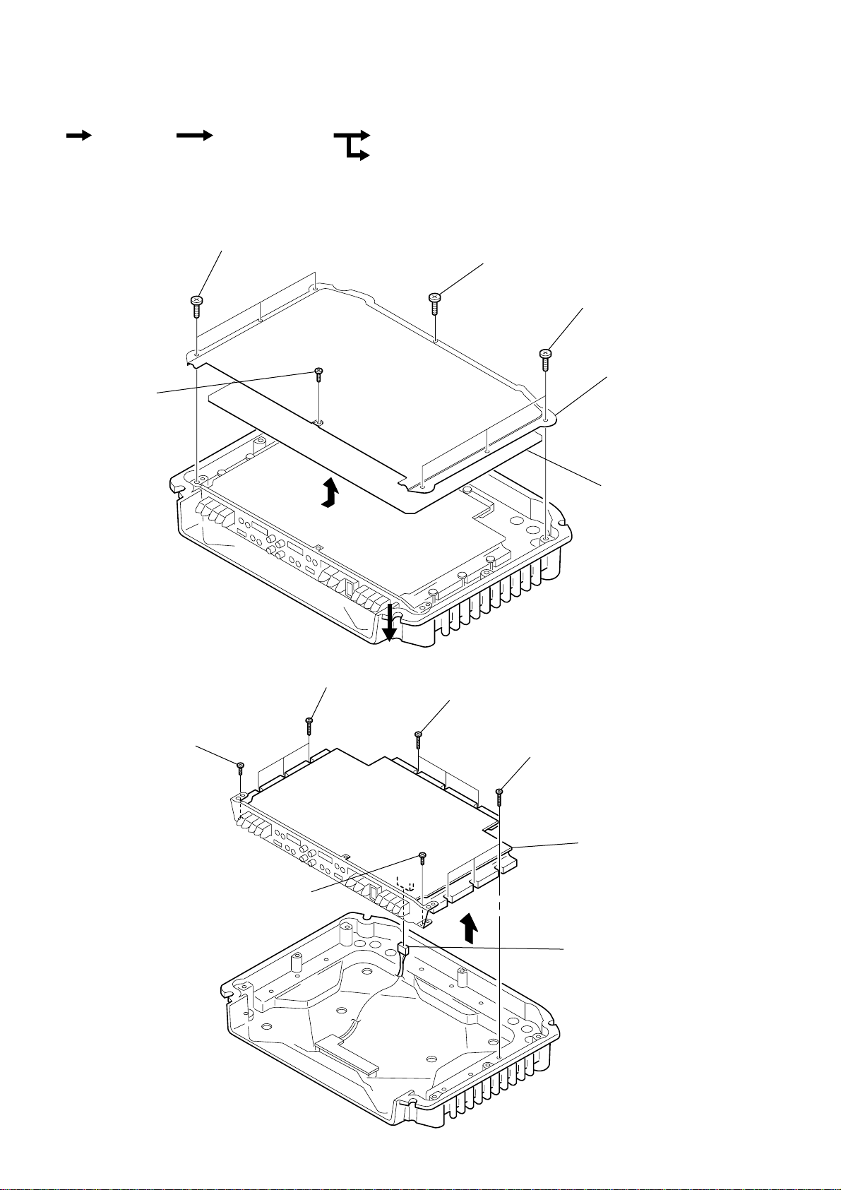
DISASSEMBLY
• The equipment can be removed using the following procedure.
Set Plate, Bottom
Main Board Section
Main Board, Filter (F) Board, Filter (R) Board
LED Board
Note : Follow the disassembly procedure in the numerical order given.
2-1. PLATE, BOTTOM
3
BTP 3x6
4
P 2.6x2.8
6
BTP 3x6
2
1
BTP 3x6
5
plate, bottom
7
sheet, insulatin
2-2. MAIN BOARD SECTION
2
BTP 3x6
1
BTP 3x6
3
B.TT. 3x14
4
B.TT. 3x14
6
5
B.TT. 3x14
8
7
MAIN board
CN802
6
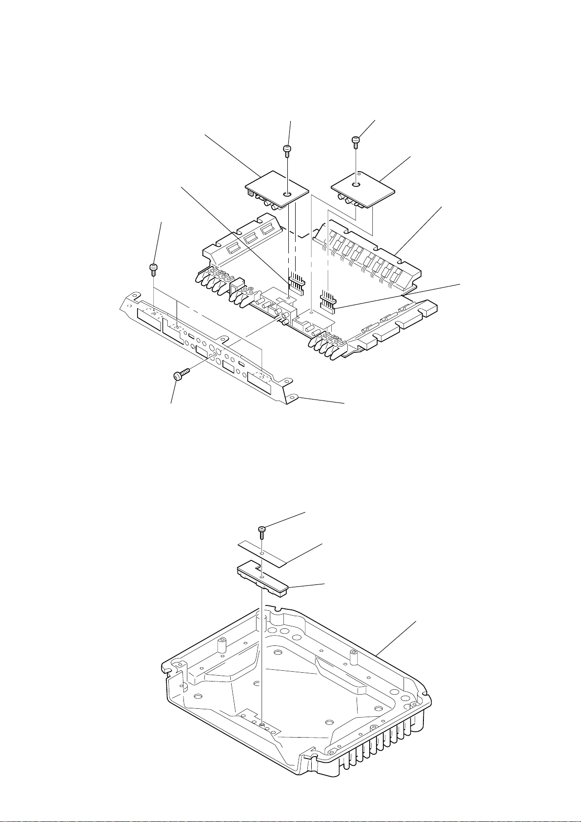
2-3. MAIN BOARD, FIL TER (F) BOARD, FILTER (R) BOARD
4
BVTT 3x5
6
FILTER (F) board
5
CNP101
2
P 3x8
7
BVTT 3x5
9
FILTER (R) board
0
MAIN board
8
CNP201
XM-754SX
2-4. LED BOARD
1
P 3x8
3
panel (4ch), front
1
BTP 3x6
2
sheet (LED), insulating
3
LED board
heat sink (main)
7
XM-754SX
SECTION 3
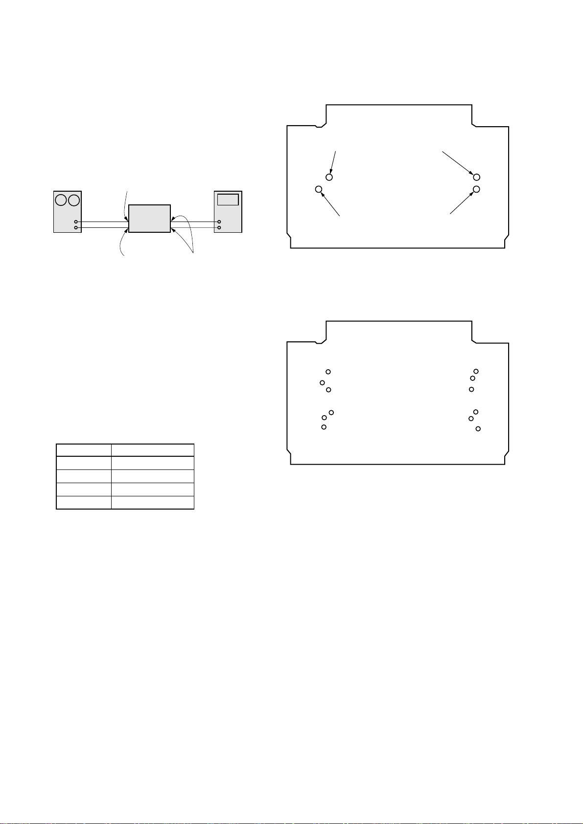
ELECTRICAL ADJUSTMENT
Bias Adjustment
Note : The Bias adjustment should be performed only if any of
Q109 and Q110 for RV104, Q209 and Q210 for RV204,
Q309 and Q310 for R V304, and Q409 and Q410 for RV404
are replaced.
Setting :
Stabilized
Power supply
B+,REM terminals
set
GND terminal test points
Procedure:
1. Rotate variable resistors RV104 (FRONT L-CH), RV204
(FRONT R-CH), RV304 (REAR L-CH) and RV404 (REAR
R-CH) full counterclockwise as seen from the pattern side to
minimize the bias current.
2. The input signal is with no signal.
3. Connect the stabilized power supply between B+ and REM
terminals and gradually increase the voltage to 14.4 V while
checking for any abnormal current.
4. Adjust R V104 (FRONT L-CH), R V204 (FR ONT R-CH), R V304
(REAR L-CH) and RV404 (REAR R-CH) so that the digital
voltmeter connected between the respective test points reads
19.5±0.5 mV.
RV Ref. No. Test points
RV104 TP11 and TP12
RV204 TP21 and TP22
RV304 TP31 and TP32
RV404 TP41 and TP42
Digital
Voltmeter
+
_
Adjustment Location :
– MAIN BOARD (CONDUCTOR SIDE) –
RV304
BIAS ADJUSTMENT
(REAR L-CH)
RV404
BIAS ADJUSTMENT
(REAR R-CH)
Test Point Location :
– MAIN BOARD (CONDUCTOR SIDE) –
TP31
TP32
TP42
TP33
TP41
TP43
RV204
BIAS ADJUSTMENT
(FRONT R-CH)
RV104
BIAS ADJUSTMENT
(FRONT L-CH)
TP22
TP12
TP21
TP23
TP11
TP13
5. After this adjustment, verify that the current value of the
stabilized power supply is 2.5±0.5 A.
(When the set is cool, more current will flow. If the observed
value is out of specification, wait unit the set is warmed up and
then perform this adjustment again.)
8
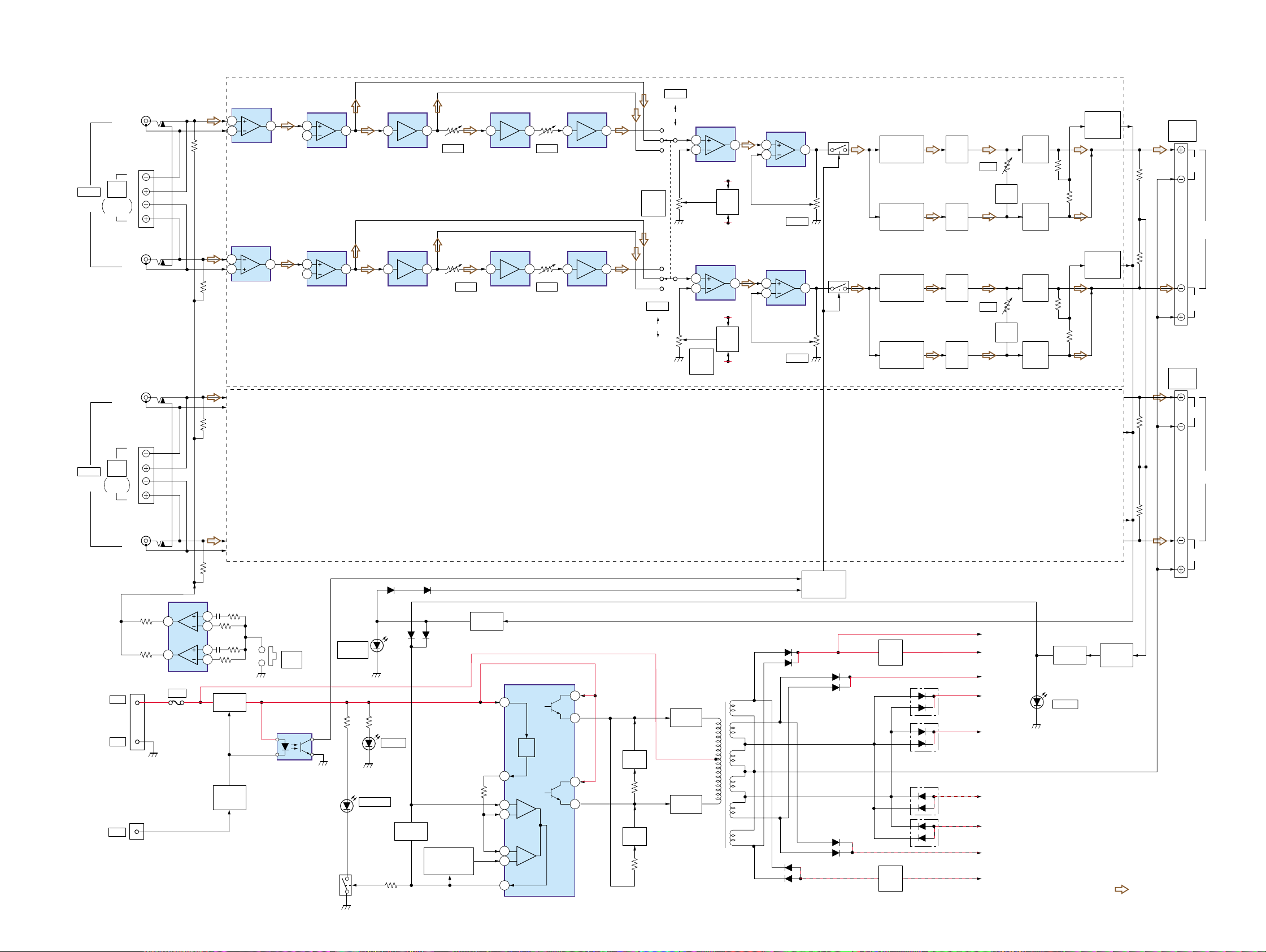
4-1. BLOCK DIAGRAM
CNJ100-1
L
(BTL)
CN101
L
HIGH
INPUT
LEVEL
INPUT
(FRONT)
(
)
FRONT
R
CNJ100-2
R
CNJ100-3
L
(BTL)
PRE AMP
IC801 (1/2)
3
2
PRE AMP
IC801 (2/2)
6
5
XM-754SX
SECTION 4
DIAGRAMS
S801-1
RV802-1
LOW
BOOST
(40Hz)
S801-2
FILTER
LPF
OFF
HPF
FILTER
LPF
OFF
HPF
PRE AMP
IC802 (1/2)
1
7
3
2
PRE AMP
IC802 (2/2)
5
6
1 3 1 6 7 2 1
7 5 7 2 1 6 7
H.P.F
IC803 (1/2)
H.P.F
IC803 (2/2)
RV801-1
FILTER
RV801-2
FILTER
L.P.F
IC804 (2/2)
L.P.F
IC805 (1/2)
RV801-3
FILTER
RV801-4
FILTER
L.P.F
IC804 (1/2)
L.P.F
IC805 (2/2)
LOW BOOST
IC806 (2/2)
5
6
LOW BOOST
IC807 (2/2)
5
6
RV802-2
LOW
BOOST
(40Hz)
(FRONT)
7
B+
(+14.2V)
LEVEL
SHIFT
Q101
B–
(–14.2V)
7
B+
(+14.2V)
LEVEL
SHIFT
Q201
B–
(–14.2V)
(REAR)
GAIN AMP
IC806 (1/2)
3
2
GAIN AMP
IC807 (1/2)
3
2
RV803-1
LEVEL
RV803-2
LEVEL
LINE
SWITCH
Q102
1
LINE
SWITCH
Q202
1
DIFFERENTIAL
AMP
Q103
DIFFERENTIAL
AMP
Q104
DIFFERENTIAL
AMP
Q203
DIFFERENTIAL
AMP
Q204
DRIVE
AMP
Q107
DRIVE
AMP
Q108
DRIVE
AMP
Q207
DRIVE
AMP
Q208
RV104
BIAS
RV204
BIAS
BIAS
Q111
BIAS
Q211
POWER
AMP
Q109
POWER
AMP
Q110
POWER
AMP
Q209
POWER
AMP
Q210
OVER LOAD
DET
Q112
OVER LOAD
DET
Q212
CN810
FRONT
SPEAKER
OUT
CN811
REAR
SPEAKER
OUT
L
BTL
R
L
INPUT
(REAR)
CN201
HIGH
LEVEL
INPUT
(
REAR
CNJ100-4
+12V
GND
REM
L
)
R
R
TEST TONE
GENERATOR
IC815
CN800
2
1
CN803
1
7
F901
40A
3
2
5
6
REG
Q901,902
POWER
ON/OFF
Q903
SW805
TEST
TONE
DC DET
IC902
D809
OVER
CURRENT
(PROTECTOR)
THERMAL
(PROTECTOR)
SWITCH
Q808
D828 D829
D822
D808
POWER
D811
LED DRIVE
Q809
D823
TEMP.DET
THN801,804-807,
THP802,803
LED DRIVE
Q812,813
DC-DC CONVERTER
12
REF.
REG
14
1
2
15
16
3
IC901
BTL
R
SWITCH
CONTROL
Q801,802
D903,904
RECT
D903
D905,906
D911,912
D917,918
RECT
D905
D906
RECT
RECT
D911
D912
DC-DC
CONVERTER
TRANSFORMER
11
10
DRIVER
Q908
8
9
DRIVER
Q909
INVERTER
Q904,905
INVERTER
Q906,907
T801
D904
D917
D918
B+
REG
Q910
B–
REG
Q911
D907
D909
D907-910
RECT
D908
D910
B+
(+23.5V)
B+
(+14.2V)
B+
(+42V)
B+
(+36V)
B+
(+36V)
B–
(–35V)
B–
(–35V)
B–
(–42V)
B–
(–14.2V)
LED DRIVE
Q810,811
D810
OFFSET
(PROTECTOR)
OFFSET
DET
Q803-805
• Signal path
: AUDIO
• Front-ch : same as Rear-ch
99
 Loading...