Sony XM-754-HX Service manual
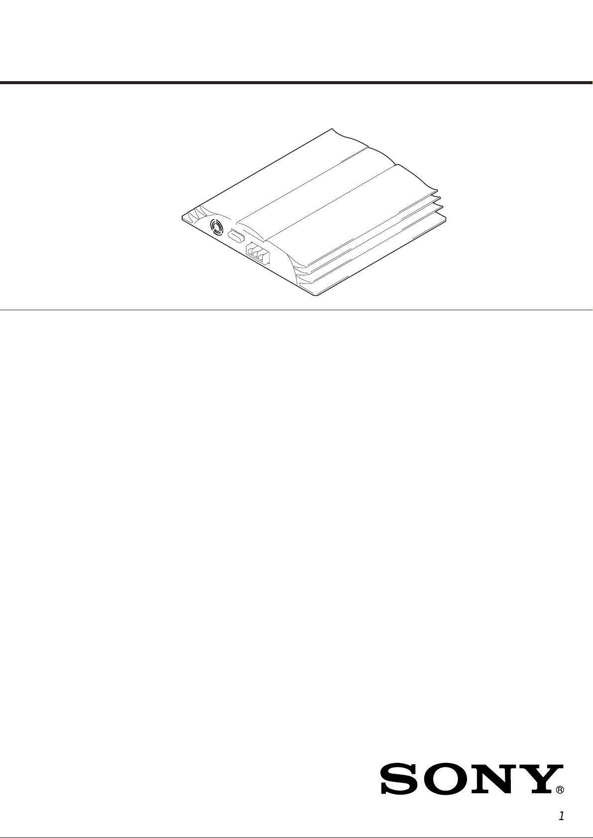
XM-754HX
SERVICE MANUAL
Ver 1.1 2001. 08
SPECIFICATIONS
AUDIO POWER SPECIFICATIONS (US model)
POWER OUTPUT AND TOTAL HARMONIC DISTORTION
75 watts per channel minimum continuous average power into
4 ohms, both channels driven from 20 Hz to 20 kHz with no more
than 0.04% total harmonic distortion per Car Audio Ad Hoc
Committee standards.
US Model
Canadian Model
AEP Model
UK Model
E Model
Other Specifications
Circuit system OTL (output transformerless) circuit
Inputs RCA pin jacks
Outputs Speaker terminals
Speaker impedance
Maximum outputs (HI-CURRENT/HI-VOLTAGE)
Rated outputs (HI-CURRENT/HI-VOLTAGE)
(supply voltage at 14.4 V)
Frequency response
Pulse power supply
High level input connector
1* – 8 Ω (stereo)
2* – 8 Ω (when used as a bridging amplifier)
Four speakers :
90/170 W x 4 (at 4 Ω)
Three speakers :
90 W x 2 + 250W x 1 / 170W x 2 + 400W x 1
(at 4 Ω)
Two speakers :
250/400 W x 2 (at 4 Ω)
Four speakers :
35/75 W x 4 (20 Hz – 20 kHz, 0.04% THD,
at 4 Ω)
50/100 W x 4 (20 Hz – 20 kHz, 0.1% THD,
at 2 Ω)
Two speakers :
100/200 W x2 (20 Hz – 20 kHz, 0.1% THD,
at 4 Ω)
5 Hz – 50 kHz (
+0.5
–3
dB)
Harmonic distortion
0.005% or less (at lkHz, 4 Ω)
Input level adjustment range
0.2 – 4.0 V (RCA pin jacks)
0.4 – 8.0 V (High level input)
High-pass filter 50 – 200 Hz, –12 dB/oct
Low-pass filter 50 – 200 Hz, –12 dB/oct
Low boost 0 – 10 dB (40 Hz)
Power requirements 12 V DC car battery (negative ground)
Power supply voltage
10.5 – 16 V
Current drain at rated output : 40 A
(4Ω HI-VOLTAGE mode)
Remote input : 1.5 mA
Dimensions Approx. 258 x 50 x 320 mm (w/h/d)
(10 l/4 x 2 x 12 5/8 in.) not incl. projecting parts and
controls
Mass Approx. 3.5 kg (7 lb. 11 oz.) not incl. accessories
Supplied accessories
Mounting screws (4),
Terminal cap (1)
Design and specifications are subject to change without notice.
* HI-CURRENT only
9-925-796-12
2001H0400-1
© 2001. 8
STEREO POWER AMPLIFIER
Sony Corporation
e Vehicle Company
Shinagawa Tec Service Manual Production Group
1
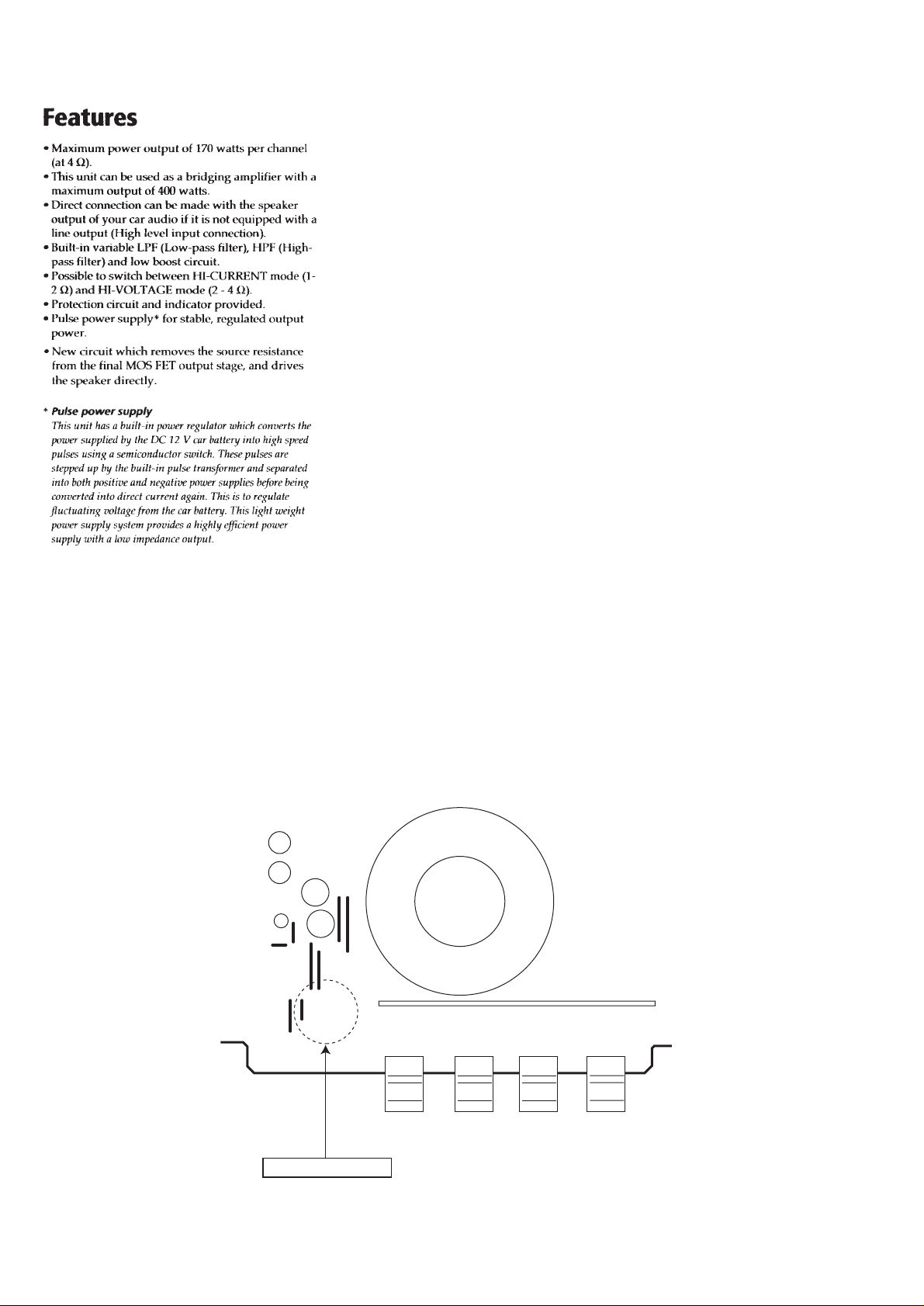
TABLE OF CONTENTS
Specifications ............................................................................. 1
1. SERVICING NOTE....................................................... 2
2. GENERAL ....................................................................... 3
3. DISASSEMBLY
3-1. Bottom Plate, Panel (Front), Panel (Rear),
SP (Front) Board, SP (Rear) Board Removal ..............5
3-2. Amplifier Board Removal ............................................ 5
4. ELECTRICAL ADJUSTMENT................................. 6
5. DIAGRAMS
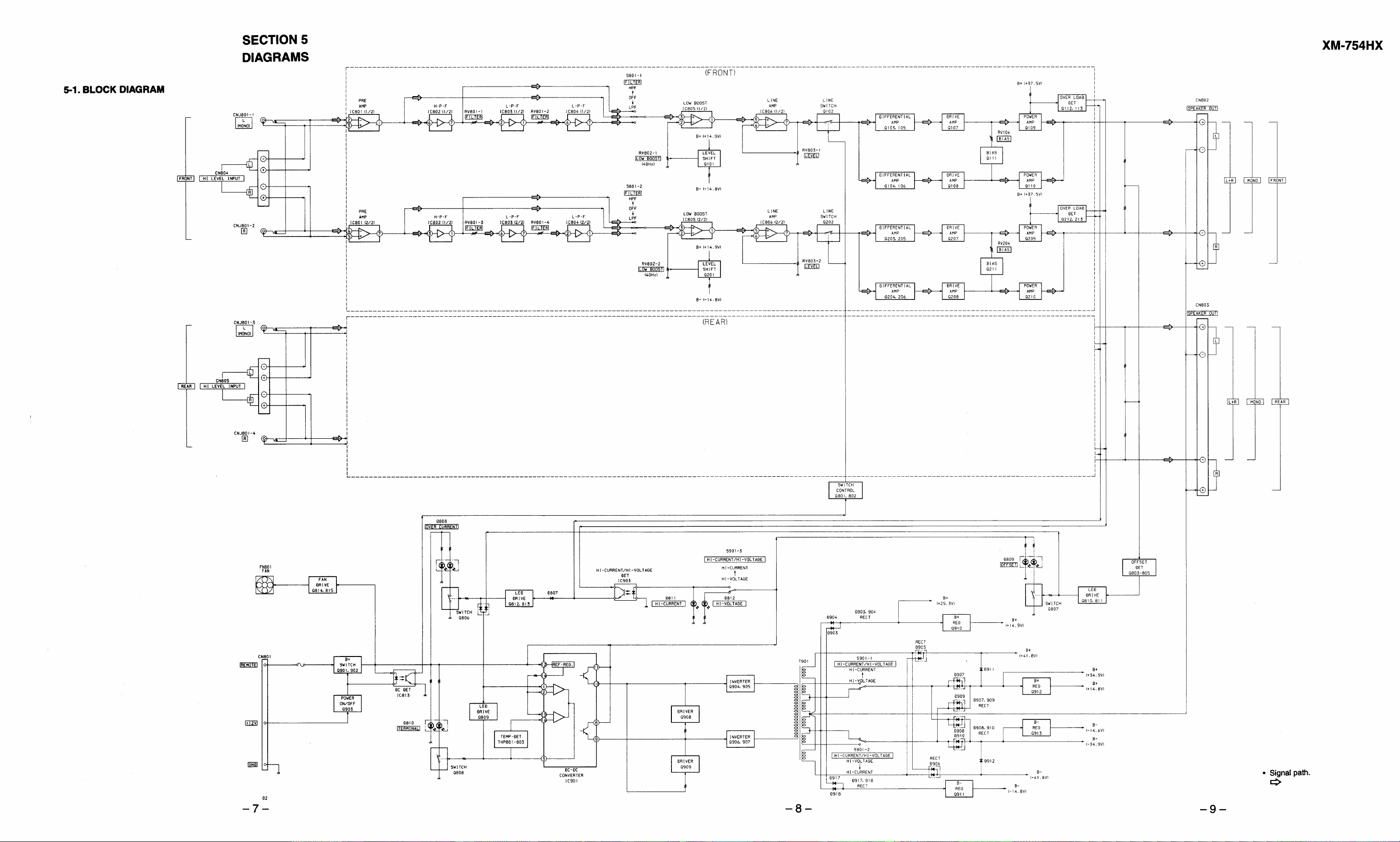
5-1. Block Diagram..............................................................7
5-2. Printed Wiring Boards ................................................ 10
5-3. Schematic Diagram.....................................................15
6. EXPLODED VIEW...................................................... 17
7. ELECTRICAL PARTS LIST.................................... 18
SECTION 1
SERVICING NOTE
CANCELLING THE PROTECTOR DURING SERVICING
Cut JW132 on the amplifier board to cancel the protector.
After servicing always be sure to return JW132 to its original state.
T901
JW167
JW131
JW168
JW132
PROTECTOR OFF
– 2 –
SECTION 2
GENERAL
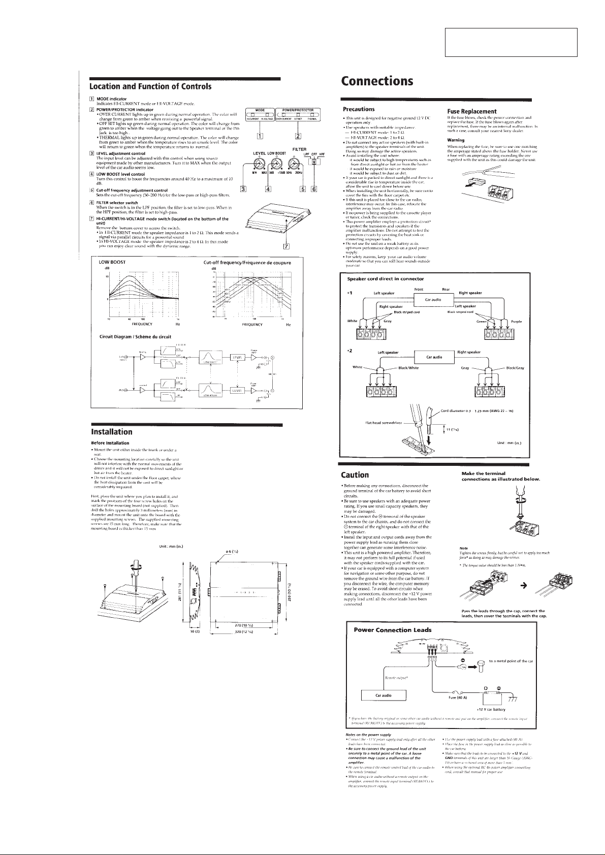
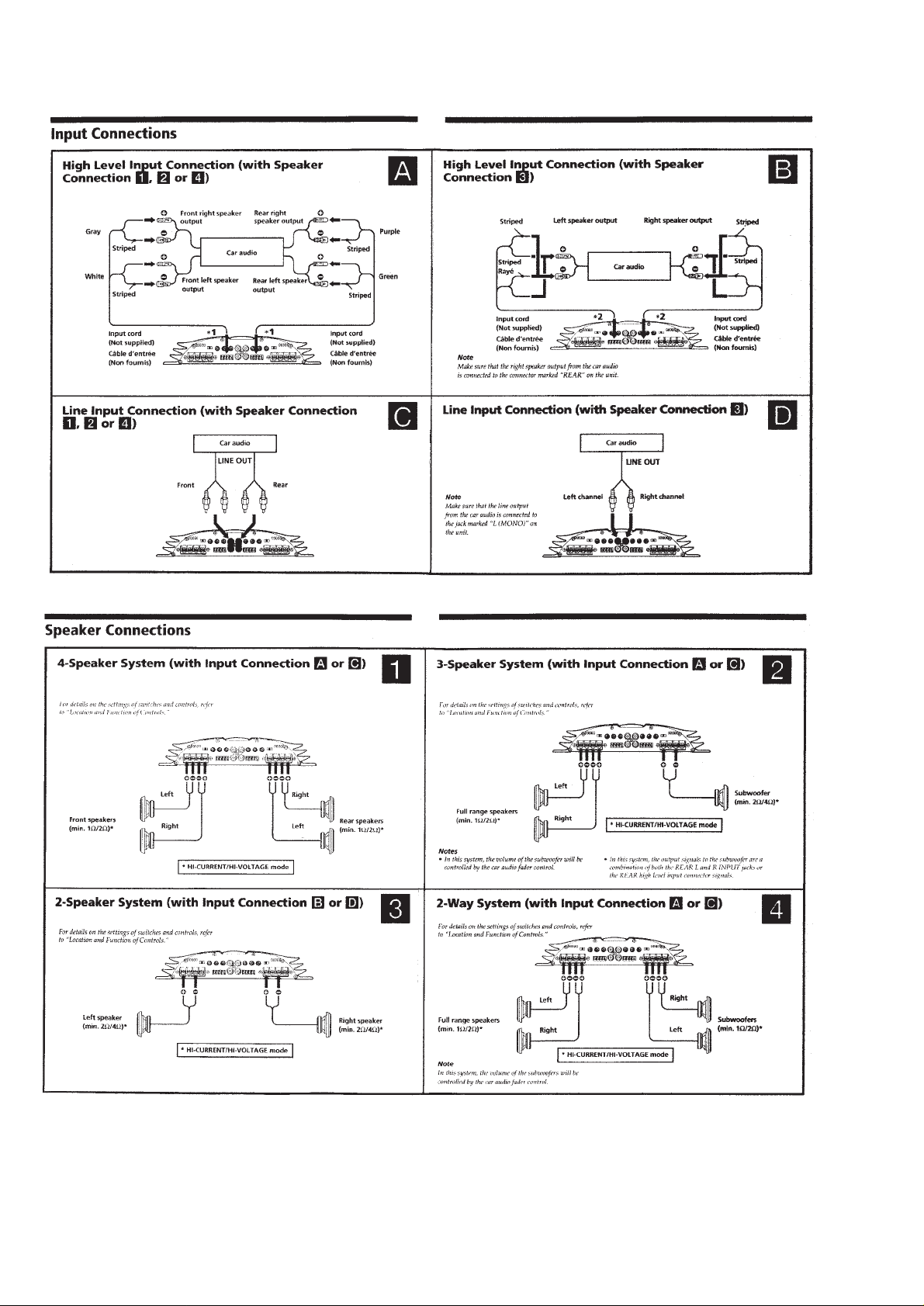
This section is extracted from
instruction manual.
– 3 –
– 4 –
SECTION 3
)
r
SECTION 4
DISASSEMBLY
Note : Follow the disassembly procedure in the numerical order given.
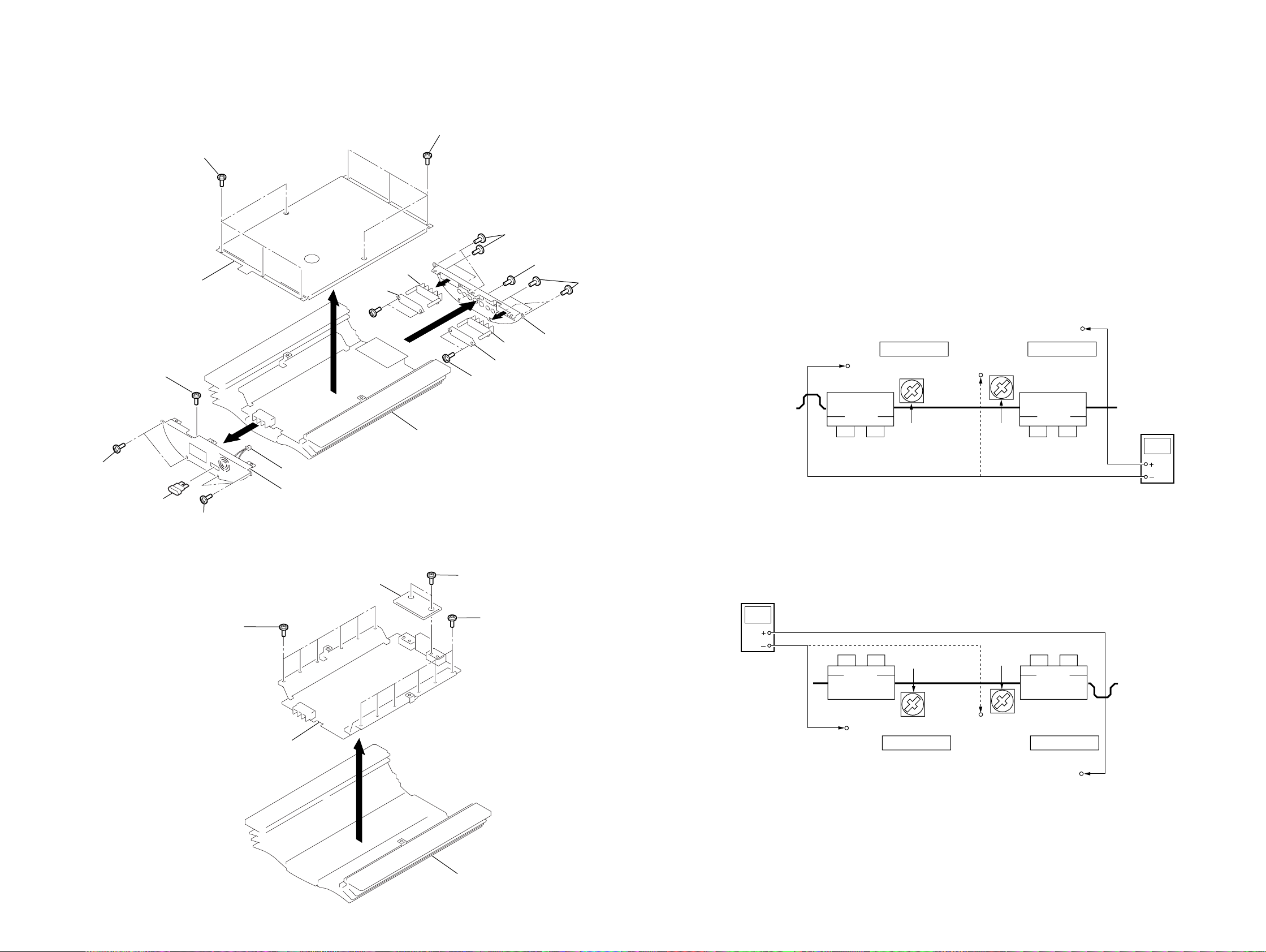
3-1. BOTTOM PLATE, PANEL (FRONT), PANEL (REAR), SP (FRONT) BOARD,
SP (REAR) BOARD REMOVAL
1
Screws (+BTP 3X5)
1
Screws (+BTP 3X5)
CN802
2
Bottom plate
4
Screw
(+BTP 3X8)
!º
SP (front)
board
9
Screws
!¡
Screws
!™
7
Screws
(+BTP 3X8)
7
Screw (+BTP 3X8)
8
CN803
SP (rear) board
Panel (rear)
7
Screws
(+BTP 3X8
ELECTRICAL ADJUSTMENT
Bias Adjustment
Procedure :
1. Rotare semi-fixed resistors RV104, RV204, RV304 and RV404
fully counterclockwise as viewed from the component side
2. No signal is entered, as input signal.
3. Apply the source voltage 14.4V between +12V, REMOTE and
GND terminals.
4. Adjust the RV104 (FRONT L-CH), RV204 (FRONT R-CH),
RV304 (REAR L-CH) and RV404 (REAR R-CH) so that the
digital voltmeter reading becomes the adjustment limits below.
Adjustment Limits : 3 ± 0.3mV
Adjustment Location :
[AMPLIFIER BOARD] (Component side)
– FRONT –
R143
TP101
TP202
R243
TP201
4
Screws
(+BTP 3X8)
3
Auto fuse (40A)
4
Screws (+BTP 3X8)
3-2. AMPLIFIER BOARD REMOVAL
3
Screws
(+P 4X10)
3
Amplifier board
5
Connector
6
Panel (front)
2
High level board
Heat sink
1
Screws
(+BTP 3X5)
3
Screws
(+P 4X10)
digital
RV104
L-CH
RV204
R-CH
voltmete
– REAR –
digital
voltmeter
R-CH
L-CH
TP301
RV304
R343 R443
RV404
TP401
Heat sink
– 5 – – 6 –
TP402
 Loading...