

Sony XM-5150-GSX Service manual
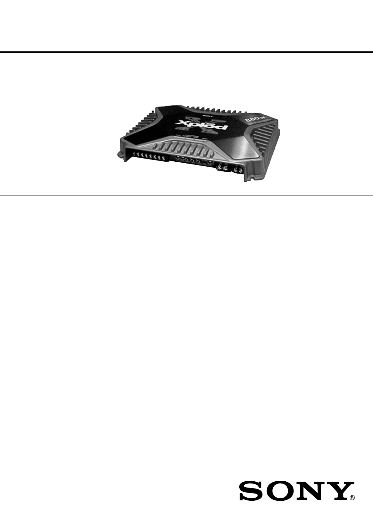
XM-5150GSX
SERVICE MANUAL
Ver 1.0 2001. 12
SPECIFICATIONS
AUDIO POWER SPECIFICATIONS
POWER OUTPUT AND TOTAL HARMONIC DISTORTION
40 watts/150 watts per channel minimum continuous average power into
4 ohms, 5channels driven from 50 Hz to 20 kHz/20 Hz to 300 Hz
(subwoofer) with no more than 0.04% total harmonic distortion per Car
Audio Ad Hoc Committee Standards.
US Model
Canadian Model
Other Specifications
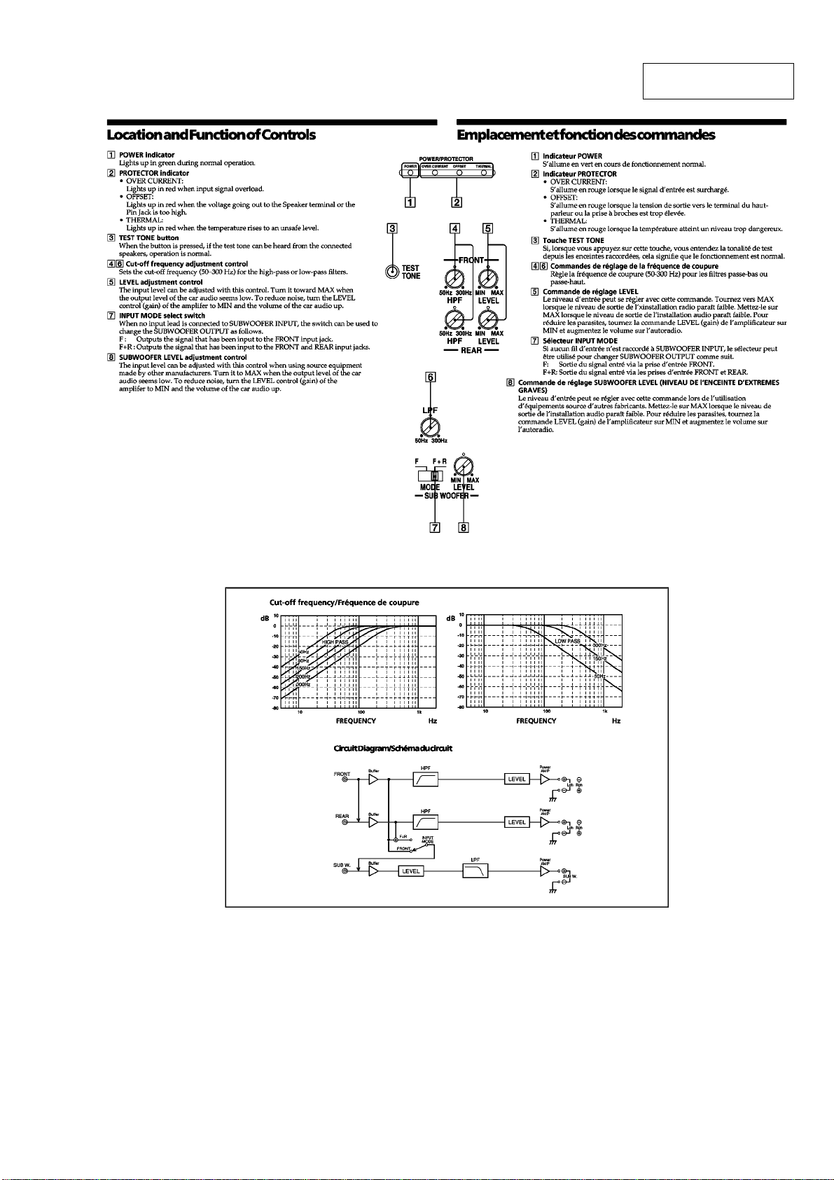
Circuit system OTL (output transformerless) circuit
Inputs RCA pin jacks
Outputs Speaker terminals
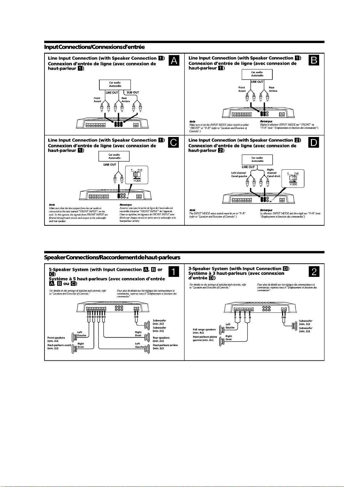
Speaker impedance 2 – 8 Ω (stereo)
Maximum outputs 80 watts × 4 + 300 watts × 1 (at 4 Ω)
Rated outputs (supply voltage at 14.4 V)
5 Speakers: 40 watts × 4 (50 Hz – 20 kHz, 0.04%
3 Speakers: 120 watts × 2 (50 Hz – 20 kHz, 0.1%
Frequency response 5 Hz – 50 kHz ( dB)
Harmonic distortion 0.005% or less (at 1 kHz, 4 Ω)
Pulse power supply
4 – 8 Ω (when used as a bridging amplifier)
THD, at 4 Ω) + 150 watts × 1 (20 –
300 Hz, 0.04% THD, at 4 Ω)
60 watts × 4 (50 Hz – 20 kHz, 0.1%
THD, at 2 Ω) + 180 watts × 1 (20 –
300 Hz, 0.1% THD, at 2 Ω)
THD, at 4 Ω) + 150 watts × 1 (20 –
300 Hz, 0.04% THD, at 4 Ω)
+0
–3
Input level adjustment range
High-pass filter 50 – 300 Hz, –12 dB/oct
Low-pass filter 50 – 300 Hz, –12 dB/oct
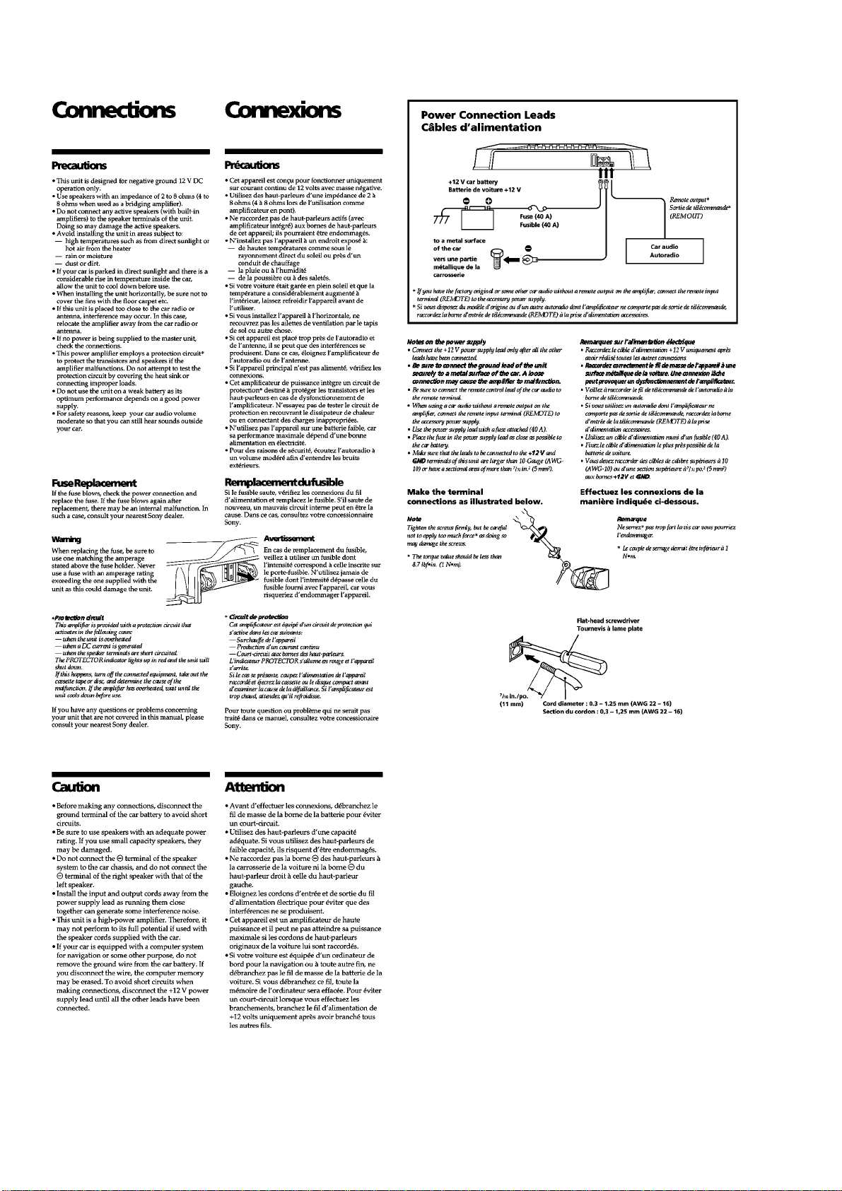
Power requirements 12 V DC car battery
Power supply voltage 10.5 – 16 V
Current drain at rated output : 42 A
Dimensions Approx. 358 × 50 × 264 mm
Mass Approx. 3.5 kg (7 lb. 11 oz.) not incl. accessories
Supplied accessories Mounting screws (4)
Design and specifications are subject to change without
notice.
0.2 – 6.0 V (RCA pin jacks)
(negative ground)
Remote input : 1.0 mA
(w/h/d) (14
projecting parts and controls
1/8 × 2 × 10 1/2 in.) not incl.
9-873-437-01
2001L0400-1
© 2001. 12
STEREO POWER AMPLIFIER
Sony Corporation
e Vehicle Company
Published by Sony Engineering Corporation
1

XM-5150GSX
TABLE OF CONTENTS
1. GENERAL
Location and Function of Controls.......................................... 3
Connections ............................................................................. 4
2. DISASSEMBLY
2-1. Plate, Bottom....................................................................... 6
2-2. Amp Board Section ............................................................. 6
2-3. Amp Board, HPF Board, LPF Board .................................. 7
2-4. LED Board .......................................................................... 7
3. ELECTRICAL ADJUSTMENT...................................... 8
4. DIAGRAMS
4-1. Block Diagram .................................................................... 9
4-2. Printed Wiring Boards –HPF, LPF, LED Section– ........... 10
4-3. Schematic Diagram –HPF, LPF, LED Section–................ 11
4-4. Schematic Diagram –Amp Section (1/2)– ........................ 12
4-5. Schematic Diagram –Amp Section (2/2)– ........................ 13
4-6. Printed Wiring Board –Amp Section– ..............................14
5. EXPLODED VIEWS
5-1. Heat Sink (Main) Section.................................................. 16
5-2. Amp Board Section ........................................................... 17
6. ELECTRICAL PARTS LIST ........................................ 18
Notes on Chip Component Replacement
• Never reuse a disconnected chip component.
• Notice that the minus side of a tantalum capacitor may be dam-
aged by heat.
SAFETY-RELATED COMPONENT WARNING!!
COMPONENTS IDENTIFIED BY MARK 0 OR DOTTED LINE
WITH MARK 0 ON THE SCHEMATIC DIAGRAMS AND IN
THE PARTS LIST ARE CRITICAL TO SAFE OPERATION.
REPLACE THESE COMPONENTS WITH SONY P ARTS WHOSE
PART NUMBERS APPEAR AS SHOWN IN THIS MANUAL OR
IN SUPPLEMENTS PUBLISHED BY SONY.
2
ATTENTION AU COMPOSANT AYANT RAPPORT
À LA SÉCURITÉ!!
LES COMPOSANTS IDENTIFIÉS P AR UNE MARQUE 0 SUR LES
DIAGRAMMES SCHÉMATIQUES ET LA LISTE DES PIÈCES
SONT CRITIQUES POUR LA SÉCURITÉ DE FONCTIONNEMENT.
NE REMPLACER CES COMPOSANTS QUE PAR DES PIÈCES
SONY DONT LES NUMÉROS SONT DONNÉS DANS CE MANUEL
OU DANS LES SUPPLÉMENTS PUBLIÉS PAR SONY.
SECTION 1
GENERAL
XM-5150GSX
This section is extracted
from instruction manual.
3
XM-5150GSX
4
XM-5150GSX
5
XM-5150GSX
SECTION 2
DISASSEMBLY
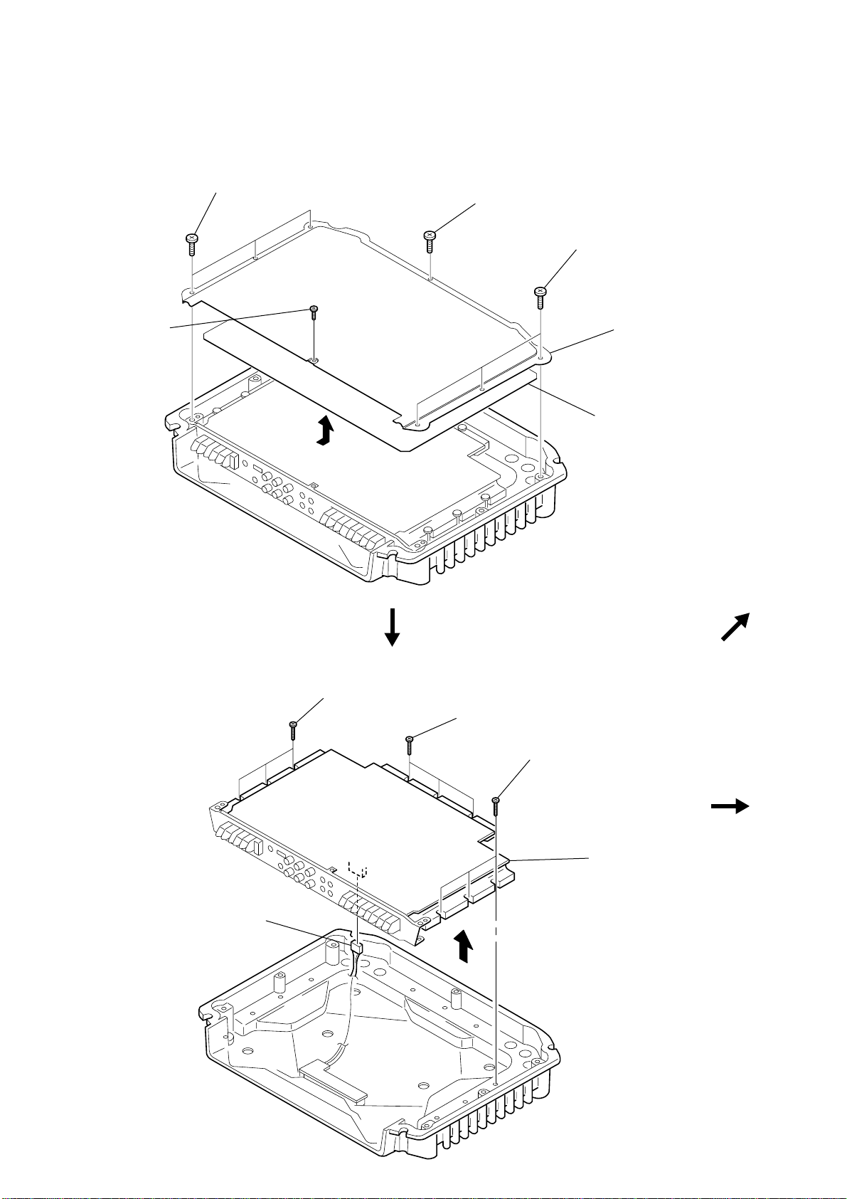
Note : Follow the disassembly procedure in the numerical order given.
2-1. PLATE, BOTTOM
4 P 2.6x2.8
3 BTP 3x6
6
2 BTP 3x6
1 BTP 3x6
5 plate, bottom
7 sheet, insulating
2-2. AMP BOARD SECTION
6 CNP808
1 B.TT. 3x14
2 B.TT. 3x14
3 B.TT. 3x14
5 AMP board section
4
6
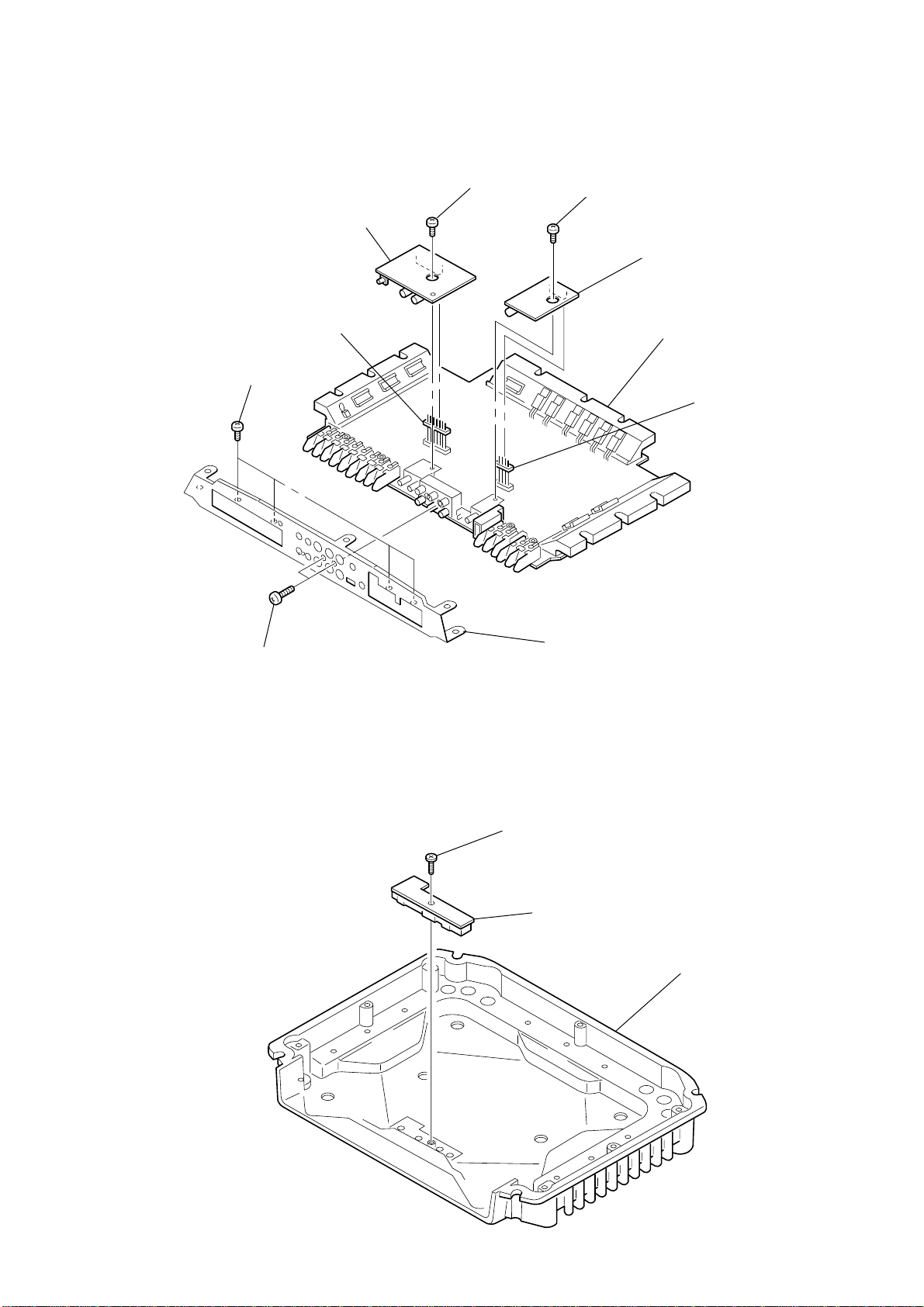
2-3. AMP BOARD, HPF BOARD, LPF BOARD
XM-5150GSX
2 P 3x8
6 HPF board
5 CNP806
4 BVTT 3x5
7 BVTT 3x5
9 LPF board
0 AMP board
8 CNP807
2-4. LED BOARD
1 P 3x8
3 panel (5ch), front
1 BTP 3x6
2 LED board
heat sink (main)
7
XM-5150GSX
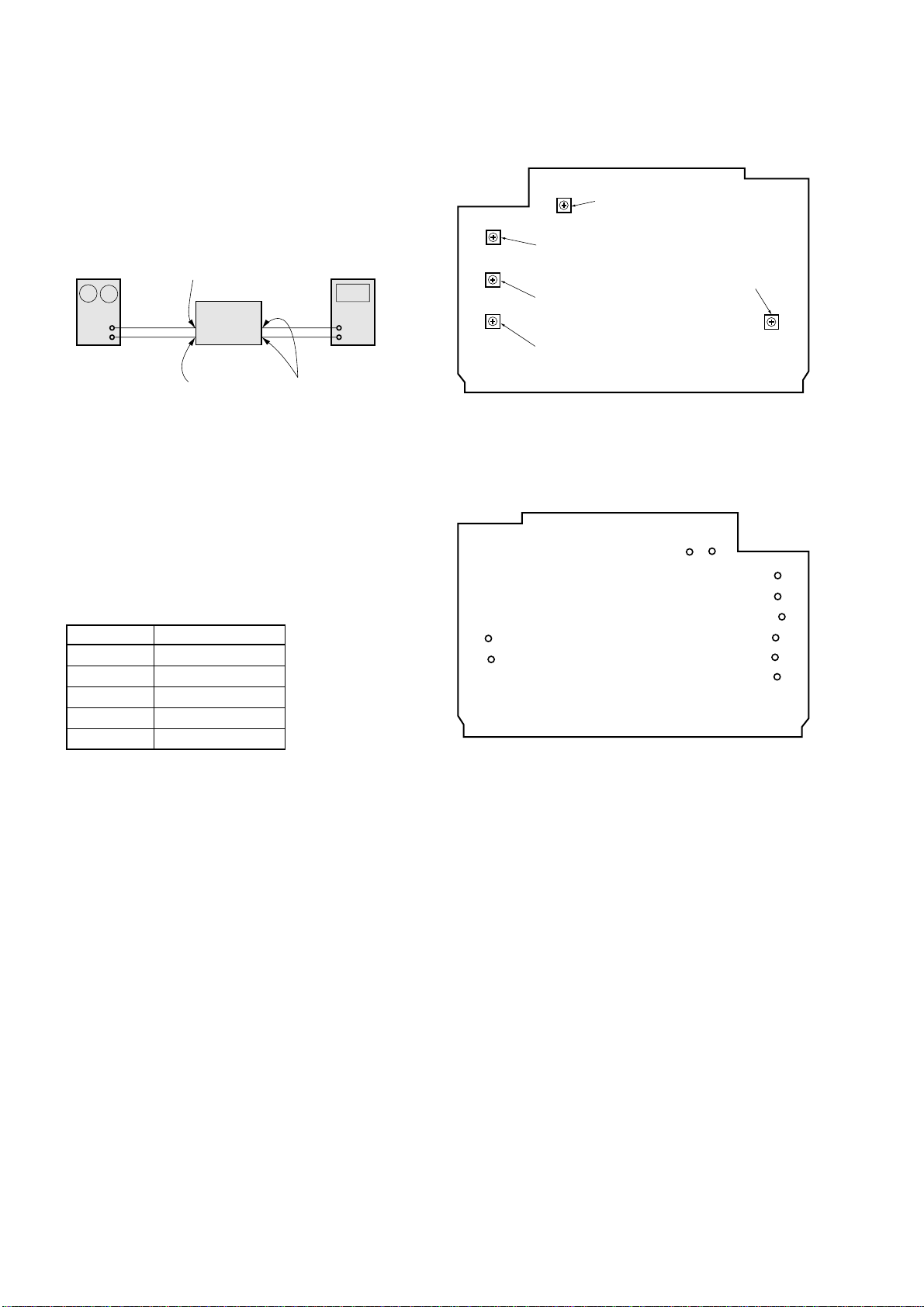
SECTION 3
ELECTRICAL ADJUSTMENT
Bias Adjustment
Note : The Bias adjustment should be performed only if any of
Q106, Q107, Q206, Q207, Q306, Q307, Q406, Q407, Q506,
Q507, Q509 and Q510 are replaced.
Setting :
Stabilized
Power supply
B+,REM terminals
set
GND terminal test points
Procedure :
1. Rotate the variable resistors VR101, VR201, VR301, VR401
and VR501 fully in the clockwise direction to minimize the
idling current of the stabilized power supply.
2. The input signal is to be no signal.
3. Set the power voltage to +14.4 V, and turn the remote mode ON
(Connect between the REM terminal and B+ terminal).
4. Connect on digital voltmeter between each test points.
5. Adjust VR101, VR201, VR301 and VR401 so that the digital
voltmeter reading is 5 ± 0.5 mV.
6. Adjust VR501 so that the digital voltmeter reading is
3.5 ± 0.5 mV.
VR Ref. No. Test points
VR101 TP101 and TP102
VR201 TP201 and TP202
VR301 TP301 and TP302
VR401 TP401 and TP402
VR501 TP501 and TP502
Digital
Voltmeter
+
_
Adjustment Location :
– AMP BOARD (COMPONENT SIDE) –
BIAS ADJUSTMENT
(REAR L-CH)
BIAS ADJUSTMENT
(FRONT R-CH)
BIAS ADJUSTMENT
(FRONT L-CH)
Test Point Location :
– AMP BOARD (CONDUCTOR SIDE) –
TP502
TP501
VR401
BIAS ADJUSTMENT
(REAR R-CH)
VR301
VR201
VR101
VR501
BIAS ADJUSTMENT
(SUB WOOFER)
TP401TP402
TP301
TP302
TP201
TP202
TP101
TP102
8
 Loading...