Sony XM-405-EQX Service manual

XM-405EQX
SERVICE MANUAL
SPECIFICATIONS
AUDIO POWER SPECIFICATIONS (US, Canadian model)
POWER OUTPUT AND TOTAL HARMONIC DISTORTION
40 watts/100 watts per channel minimum continuous average power into
4 ohms, 5 channels driven from 20 Hz to 20 kHz/200 Hz with no more
than 0.04% total harmonic distortion per Car Audio Ad Hoc Committee
standards.
US Model
Canadian Model
AEP Model
UK Model
E Model
Other Specifications
Circuit system OTL (output transformerless) circuit
Inputs RCA pin jacks
Outputs Speaker terminals
Speaker impedance 2 – 8 Ω (stereo)
Maximum outputs 80 watts × 4 + 200 watts × 1 (at 4 Ω)
Rated outputs (supply voltage at 14.4 V)
5 Speakers: 40 watts × 4 (20 Hz – 20 kHz, 0.04%
3 Speakers: 100 watts × 2 (20 Hz – 20 kHz, 0.1%
Frequency response 5 Hz – 100 kHz ( dB)
Harmonic distortion 0.005% or less (at 1 kHz, 4 Ω)
Pulse power supply
High level input connector
4 – 8 Ω (when used as a bridging
amplifier)
THD, at 4 Ω) + 100 watts × 1 (20 –
200 Hz, 0.04% THD, at 4 Ω)
50 watts × 4 (20 Hz – 20 kHz, 0.1%
THD, at 2 Ω) + 125 watts × 1 (20 –
200 Hz, 0.1% THD, at 2 Ω)
THD, at 4 Ω) + 100 watts × 1 (20 –
200 Hz, 0.04% THD, at 4 Ω)
+0
–3
Input level adjustment range
High-pass filter 50 – 200 Hz, –12 dB/oct
Low-pass filter 50 – 200 Hz, –12 dB/oct
Low boost 0 – 10 dB (40 Hz)
Power requirements 12 V DC car battery
Power supply voltage 10.5 – 16 V
Current drain at rated output: 33 A
Dimensions Approx. 260 × 55 × 450 mm
Mass Approx. 4.7 kg (10 lb. 6 oz.) not incl.
Supplied accessories Mounting screws (4),
Design and specifications are subject to change without notice.
Notes on Chip Component Replacement
• Never reuse a disconnected chip component.
• Notice that the minus side of a tantalum capacitor may be dam-
aged by heat.
0.2 – 4.0 V (RCA pin jacks)
0.4 – 8.0 V (High level input)
(negative ground)
Remote input: 1.5 mA
(w/h/d) (10
incl. projecting parts and controls
accessories
Terminal cap (1)
1/4 × 2 1/4 × 17 3/4 in.) not
MICROFILM
STEREO POWER AMPLIFIER
– 1 –

TABLE OF CONTENTS
1. GENERAL
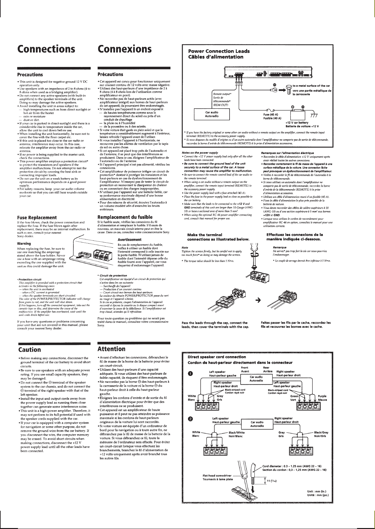
Location and Function of Controls.......................................... 3
Connections ............................................................................. 4
2. DISASSEMBLY
2-1. Bottom Plate ....................................................................... 6
2-2. Panel (A).............................................................................6
2-3. Panel (B)............................................................................. 7
2-4. AMP/Power Board .............................................................7
2-5. Control Panel Block ........................................................... 8
3. DIAGRAMS
3-1. Block Diagram –AMP Section–......................................... 9
3-2. Block Diagram –Power Section– .....................................11
3-3. Printed Wiring Board –AMP Section–.............................13
3-4. Schematic Diagram –AMP Section–................................ 15
3-5. Printed Wiring Board –Power Section– ........................... 17
3-6. Schematic Diagram –Power Section– ..............................19
3-7. Printed Wiring Board –EQ Section– ................................ 21
3-8. Schematic Diagram –EQ Section– ................................... 21
3-9. Printed Wiring Board –Sub Section– ............................... 23
3-10. Schematic Diagram –Sub Section– .................................. 23
3-11. Printed Wiring Board –IND Section– .............................. 25
3-12. Schematic Diagram –IND Section– ................................. 26
3-13. Printed Wiring Board –LED Section–..............................27
3-14. Schematic Diagram –LED Section–.................................27
4. EXPLODED VIEWS
4-1. Heat Sink Section ............................................................. 28
4-2. Control Panel Section ....................................................... 29
5. ELECTRICAL PARTS LIST.........................................30
– 2 –

SECTION 1
GENERAL
This section is extracted
from instruction manual.
– 3 –

– 4 –

– 5 –

4
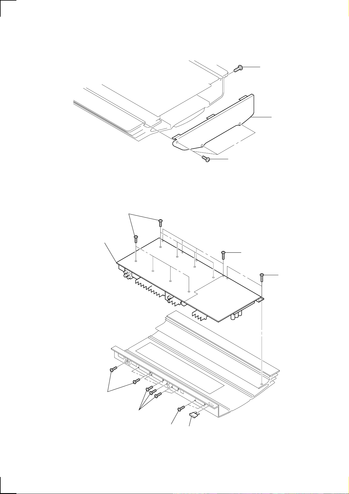
SECTION 2
)
DISASSEMBLY
Note : Follow the disassembly procedure in the numerical order given.
2-1. BOTTOM PLATE
2
BTP 3x4
1
BTP 3x5
4
bottom plate
3
BTP 3x
2-2. PANEL (A)
1
BTP 3x8
3
panel (A
2
BTP 3x8
– 6 –

2-3. P ANEL (B)
)
2-4. AMP/POWER BOARD
5
screw (3x8) (CZN-N)
2
BTP 3x8
1
BTP 3x8
3
panel (B
8
AMP/POWER
board
1 BTP 3x12
6
BVTP 3x12
7
BVTP 3x12
2
BTP 3x12
3
BTP 3x12
4
(40A)
– 7 –
fuse

2-5. CONTROL PANEL BLOCK
2
claws
8
control panel block
1
claws
4
CNP807
7
CNJ804
3
CNP806
6
CNJ802
5
CNP808
– 8 –

XM-405EQX
SECTION 3
DIAGRAMS
3-1. BLOCK DIAGRAM — AMP SECTION —
CNJ801-1
L
INPUT
FRONT
HIGH LEVEL
INPUT
CNJ801-2
R
CN802
R-CH
L+
L–
R+
R–
R-CH
3
2
IC101
R-CH
FRONT EQ
R-CH
CN804
L+
L–
R–
R+
L
MONO-L
R
FRONT
SPEAKER
OUT
S101-1
2
1
FILTER
OFF
IC103
1
IC102
3
1
2
7
IC103
5
VR101-1,2
FILTER
VR102-1
50Hz
HFP
IC104 IC105
50HzEQ200Hz
EQ
VR103-1
200Hz
IC106
800Hz
EQ
VR104-1
800Hz
IC107
3.2kHz
EQ
VR105-1
3.2kHz
IC108
12.8kHz
EQ
VR106-1
12.8kHz
IC109
5
6
7
ON
OFF
SW102
DIRECT
IC110
21
VR107
LEVEL
Q112
MUTE
Q101-110
POWER
AMP
Q111
OVER
CURRENT
DETECT
04
SUB
WOOFER
LEVEL
CONTROL
REAR
INPUT
HIGH LEVEL
INPUT
INPUT
US, Canadian
CNJ801-3
L
CNJ801-4
R
CNJ809-1
L
CNJ809-2
R
CN803
CNJ801
1
2
IC301
3
1
2
R-CH
S501
L+
L–
5
6
3
2
R-CH
IC501
IC501
R+
R–
R-CH
INPUT
MODE
7
1
IC502
21
F+R
VR501
LEVEL
FRONTF+R
FRONT
IC502
57
REAR E Q
THE SAME AS ABOVE BLOCK DIAGRAM
VR502
FILTER
IC503
57
IC503
31
Q513
LOW
BOOST
VR503
LOW BOOST
MUTE
POWER
1
SECTION
OVER-C
OFFSET
LD801-824
(MATRIX)
LED
SCAN
Q801-804
6
4
EQUALIZER
INDICATOR
16
O1
|
|
21
6
12
D1
|
|
15
4
Q512
IC802
AC1
AC2
Q312
MUTE
MUTE
Q809, 812
3
IC801
1
1
3
R-CH
BUF
Q301-310
POWER
AMP
Q311
OVER
CURRENT
DETECT
Q808, 811
BUF
Q501-510
POWER
AMP
Q511
OVER
CURRENT
DETECT
Q818-820
OFFSET
DETECT
Q815-817
OFFSET
DETECT
· Signal path
: AUDIO
R-CH
SUB+
SUB–
CN805
L+
L–
R–
R+
CN806
L
MONO-L
R
SUB
WOOFER
SPEAKER
REAR
SPEAKER
OUT
– 9 – – 10 –

XM-405EQX
3-2. BLOCK DIAGRAM — POWER SECTION —
SWITCHING REGULATER
OSC
IC901
Q813, 814
MUTE
CONTROL
PWM
CONT
IC902
VCC
LD827
THERMAL
LD826
OFFSET
LD825
OVER
CURRENT
CN801
04
BATT
REM
TH801
TH802
Q901
VREF
Q807
LED
DRIVE
Q806
LED
DRIVE
Q805
LED
DRIVE
Q902, 903
REG
16
3
1 12
Q810
F/R +B2
B+
9
10
Q905, 906
OFFSET
OVER-C
MUTE
F/R+15V
ON/OFF
CONT.
AMP
SECTION
Q907, 909
ON/OFF
DRIVE
Q908, 910
ON/OFF
DRIVE
1
T901
Q904
5V
REG
Q911
15V
REG
Q912
–15V
REG
+5V
F/R +15V
F/R +B2
F/R +B3
F/R –B3
F/R –B2
F/R –15V
SUB +B2
SUB +B3
SUB –B3
SUB –B2
THIS NOTE IS COMMON FOR PRINTED WIRING BOARDS
AND SCHEMATIC DIAGRAMS.
(In addition to this, the necessary note is
printed in each block.)
for schematic diagrams
• All capacitors are in µF unless otherwise noted. pF: µµF
50 WV or less are not indicated except for electrolytics and
tantalums.
• All resistors are in Ω and 1/
specified.
4
W or less unless otherwise
• % : indicates tolerance.
• 2 : nonflammable resistor.
• C : panel designation.
• U : B+ Line.
• Power voltage is dc 14.4V and fed with regulated dc power
supply from +12V and REMOTE terminals.
• Voltage is dc with respect to ground under no-signal
condition.
• Voltages are taken with a VOM (Input impedance 10 MΩ).
Voltage variations may be noted due to normal production
tolerances.
• Signal path.
F : AUDIO
for printed wiring boards
• X : parts extracted from the component side.
r
•
: Through hole.
• b : Pattern from the side which enables seeing.
(The other layer’s patterns are not indicated.)
Caution:
Pattern face side: Parts on the pattern face side seen from the
(Side B) pattern face are indicated.
Parts face side: Parts on the parts face side seen from the
(Side A) parts face are indicated.
• Semiconductor Location
(AMP Board)
Ref. No. Location
D101 D-5
D102 D-4
D201 D-3
D202 D-2
D301 D-8
D302 D-7
D401 D-9
D402 D-8
D501 D-13
D502 C-12
D801 G-8
D803 F-2
IC101 H-4
IC301 H-3
IC501 H-12
IC801 E-3
IC902 E-1
Q101 C-4
Q102 D-4
Q103 C-5
Q104 C-4
Q105 A-4
Q106 A-4
Q107 C-5
Q108 C-4
Q109 B-5
Q110 B-4
Q111 A-4
Q112 D-4
Q201 D-2
Q202 D-2
Q203 D-3
Q204 C-2
Q205 A-2
Q206 A-2
Q207 C-3
Q208 C-2
Q209 A-3
Q210 B-2
Q211 A-2
Q212 E-1
Q301 D-7
Q302 D-7
Q303 C-8
Q304 C-6
Ref. No. Location
Q305 A-7
Q306 A-7
Q307 C-8
Q308 C-7
Q309 B-8
Q310 B-6
Q311 A-6
Q312 D-6
Q401 D-9
Q402 D-9
Q403 D-10
Q404 C-8
Q405 A-9
Q406 A-10
Q407 C-9
Q408 C-8
Q409 B-10
Q410 B-9
Q411 A-9
Q412 E-8
Q501 C-12
Q502 C-12
Q503 C-13
Q504 C-12
Q505 A-13
Q506 A-13
Q507 A-12
Q508 A-11
Q509 B-14
Q510 B-12
Q511 A-12
Q512 E-13
Q808 G-7
Q809 G-8
Q810 G-7
Q811 G-7
Q812 G-8
Q813 E-2
Q814 E-2
Q815 G-1
Q816 F-2
Q817 F-1
Q818 F-3
Q819 F-3
Q820 F-3
ZD801 F-2
– 11 – – 12 –
 Loading...