

Page 1

UHF SYNTHESIZED TRANSMITTER
UTX-P03
UHF WIRELESS MICROPHONE PACKAGE
UWP-D16
SERVICE MANUAL
1st Edition
Page 2

!警告
このマニュアルは,サービス専用です。
お客様が,このマニュアルに記載された設置や保守,点検,修理などを行うと感電や火災,
人身事故につながることがあります。
危険をさけるため,サービストレーニングを受けた技術者のみご使用ください。
! WARNING
This manual is intended for qualifi ed service personnel only.
To reduce the risk of electric shock, fi re or injury, do not perform any servicing other than that
contained in the operating instructions unless you are qualifi ed to do so. Refer all servicing to
qualifi ed service personnel.
! WARNUNG
Die Anleitung ist nur für qualifi ziertes Fachpersonal bestimmt.
Alle Wartungsarbeiten dürfen nur von qualifi ziertem Fachpersonal ausgeführt werden. Um die
Gefahr eines elektrischen Schlages, Feuergefahr und Verletzungen zu vermeiden, sind bei
Wartungsarbeiten strikt die Angaben in der Anleitung zu befolgen. Andere als die angegeben
Wartungsarbeiten dürfen nur von Personen ausgeführt werden, die eine spezielle Befähigung
dazu besitzen.
! AVERTISSEMENT
Ce manual est destiné uniquement aux personnes compétentes en charge de l’entretien. Afi n
de réduire les risques de décharge électrique, d’incendie ou de blessure n’effectuer que les
réparations indiquées dans le mode d’emploi à moins d’être qualifi é pour en effectuer d’autres.
Pour toute réparation faire appel à une personne compétente uniquement.
UTX-P03
Page 3

注意
注意
FÖRSIKTIGHET!
指定以外の電池に交換すると,破裂する危険があります。
必ず指定の電池に交換してください。
使用済みの電池は,国または地域の法令に従って
処理してください。
CAUTION
Danger of explosion if battery is incorrectly replaced.
Replace only with the same or equivalent type recommended by the manufacturer.
When you dispose of the battery, you must obey the
law in the relative area or country.
ATTENTION
Il y a danger d’explosion s’il y a remplacement incor-
rect de la batterie. Remplacer uniquement avec
une batterie du même type ou d’un type équivalent
recommandé par le constructeur.
Lorsque vous mettez la batterie au rebut, vous devez
respecter la législation en vigueur dans le pays ou la
région où vous vous trouvez.
Fara för explosion vid felaktigt placerat batteri.
Byt endast mot samma eller likvärdig typ av batteri,
enligt tillverkarens rekommendationer.
När du kasserar batteriet ska du följa rådande lagar
för regionen eller landet.
PAS PÅ
Fare for eksplosion, hvis batteriet ikke udskiftes
korrekt.
Udskift kun med et batteri af samme eller tilsvarende
type, som er anbefalet af fabrikanten.
Når du bortskaffer batteriet, skal du følge
lovgivningen i det pågældende område eller land.
HUOMIO
Räjähdysvaara, jos akku vaihdetaan virheellisesti.
Vaihda vain samanlaiseen tai vastaavantyyppiseen,
valmistajan suosittelemaan akkuun.
Noudata akun hävittämisessä oman maasi tai
alueesi lakeja.
VORSICHT
Explosionsgefahr bei Verwendung falscher Batterien.
Batterien nur durch den vom Hersteller empfohlenen
oder einen gleichwertigen Typ ersetzen.
Wenn Sie die Batterie entsorgen, müssen Sie die
Gesetze der jeweiligen Region und des jeweiligen
Landes befolgen.
FORSIKTIG
Eksplosjonsfare hvis feil type batteri settes i.
Bytt ut kun med samme type eller tilsvarende
anbefalt av produsenten.
Kasser batteriet i henhold til gjeldende avfallsregler.
注意
如果更换的电池不正确,就会有爆炸的危险。
只更换同一类型或制造商推荐的电池型号。
处理电池时,必须遵守相关地区或国家的法律。
UTX-P03
1 (P)
Page 4

Page 5

Table of Contents
Manual Structure
Purpose of this manual ............................................................ 2 (E)
Related manuals ...................................................................... 2 (E)
1. Service Overview
1-1. About Destination Determination .............................1-1 (E)
1-2. Board Location ..........................................................1-1 (E)
1-3. Removal Procedure ...................................................1-2 (E)
1-3-1. Lower Case (P03)/Upper Case (P03)/
Case (P03) ........................................................ 1-2 (E)
1-3-2. CPU-458 Board ...............................................1-3 (E)
1-3-3. LCD Module .................................................... 1-3 (E)
1-3-4. RF-164 Board ..................................................1-4 (E)
1-3-5. XLA Connector Assembly ...............................1-5 (E)
1-4. Diagnosis of Failure ..................................................1-6 (E)
1-4-1. No Sound is Output/Service Area is Narrow/
There is a Noise ...............................................1-6 (E)
1-4-2. Sound is distorted ............................................1-6 (E)
1-5. Lead-free Solder ........................................................1-7 (E)
3. Spare Parts
3-1. Notes on Repair Parts ...................................................... 3-1
3-2. Exploded Views ............................................................... 3-2
3-3. Electrical Parts List .........................................................3-4
3-4. Packing Materials & Supplied Accessories ..................... 3-4
4. Block Diagrams
4-1. Circuit Description .................................................... 4-1 (E)
4-1-1. RF-164 Board ..................................................4-1 (E)
4-1-2. CPU-458 Board ...............................................4-1 (E)
4-2. Overall Block Diagrams .................................................. 4-3
Overall ............................................................................. 4-3
4-3. Frame Wiring...................................................................4-4
Frame Wiring...................................................................4-4
2. Operation Check
2-1. Preparation ................................................................2-1 (E)
2-1-1. Required Equipment ........................................2-1 (E)
2-1-2. Tool List ........................................................... 2-1 (E)
2-2. Check of Transmission Output ................................. 2-2 (E)
2-2-1. Required Equipment/Tool ................................2-2 (E)
2-2-2. Setting ..............................................................2-2 (E)
2-2-3. Procedure ......................................................... 2-3 (E)
2-3. Check of Sound Output ............................................. 2-4 (E)
2-3-1. Required Equipment/Tool ................................2-4 (E)
2-3-2. Setting ..............................................................2-4 (E)
2-3-3. Procedure ......................................................... 2-4 (E)
2-4. Check of Sound Level ............................................... 2-5 (E)
2-4-1. Required Equipment/Tool ................................2-5 (E)
2-4-2. Setting ..............................................................2-5 (E)
2-4-3. Procedure ......................................................... 2-5 (E)
2-5. Check of +48V .......................................................... 2-6 (E)
2-5-1. Required Equipment/Tool ................................2-6 (E)
2-5-2. Procedure ......................................................... 2-6 (E)
UTX-P03
1 (E)
Page 6

Purpose of this manual
Related manuals
Manual Structure
This manual is the Service Manual of the UHF Synthesized Transmitter UTX-P03.
This manual describes the information on the premise of providing the block level
service (such as service overview, diagnosis of failure, spare parts, circuit description, block diagrams, and frame wiring).
The UHF wireless microphone packages consists of the following.
. UWP-D16: UTX-B03, UTX-P03, URX-P03
The following manuals are provided for this unit in addition to this “Service Manual”.
. “Instruction Manual” CD-ROM (supplied with this unit)
This manual is necessary for installation of this unit.
. UTX-B03 Service Manual (available on request)
This manual describes the required information of service of UTX-B03.
. URX-P03 Service Manual (available on request)
This manual describes the required information of service of URX-P03.
2 (E)
UTX-P03
Page 7
Section 1
Service Overview
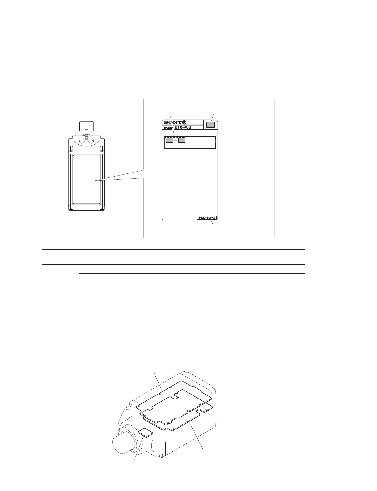
1-1. About Destination Determination
There are nine destinations in this unit.
Determine the destination by referring to the model number label and the following table.
Destinationon model
Indication of channel
number label
Model number label
Model name Destination Destination on model Indication of Part number on model
number label channel number label
UTX-P03 UC14 14 14-25 4-527-512-0X
UC30 30 30-36, 38-41 4-527-512-1X
UC42 42 42-51 4-527-512-2X
CE21 21 21-29 4-527-513-0X
CE33 33 33-40 4-527-513-1X
CE42 42 42-50 4-527-513-2X
CE51 51 51-59 4-527-513-3X
KR _ _ 4-527-514-0X
E _ _ 4-527-515-0X
Part number on model number label
(Example) Destination: UC
1-2. Board Location
CPU-458 board
UTX-P03
RF-164 board
CN-3708 board
1-1 (E)
Page 8
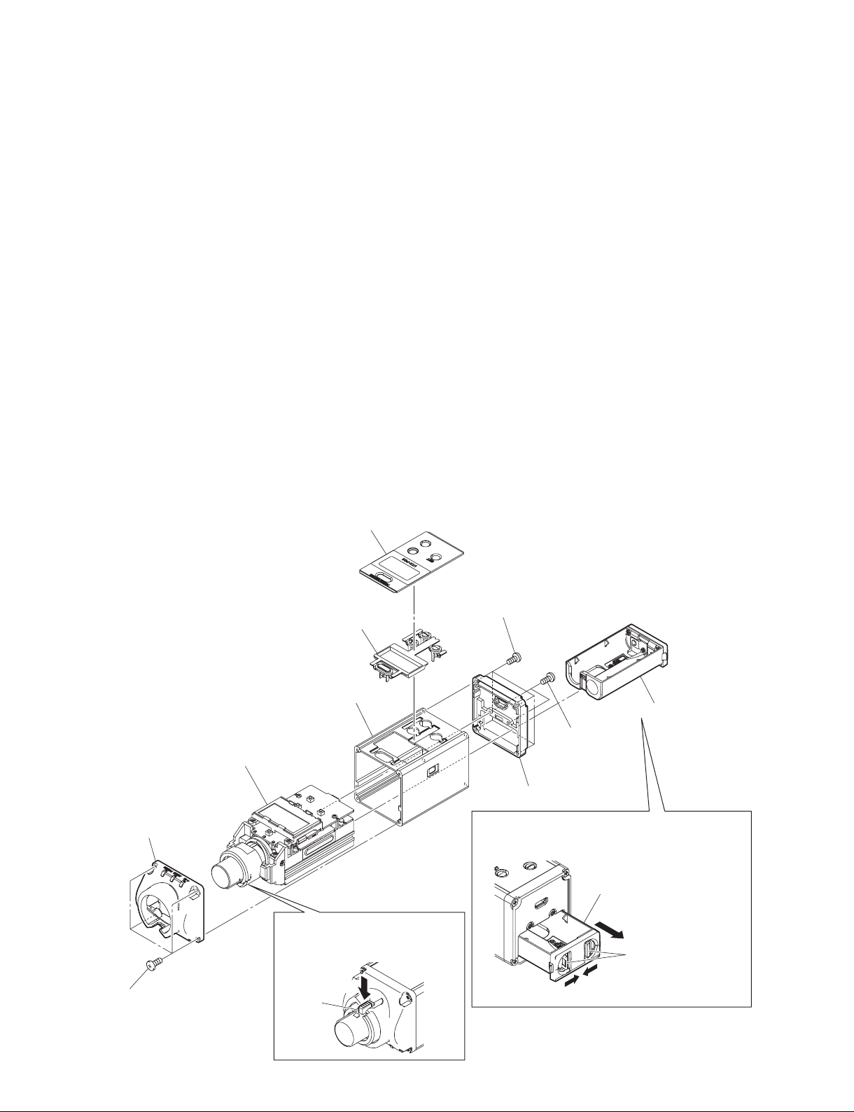
1-3. Removal Procedure
Tighten the following screws to the tightening torques as described below.
Tightening torque:
. M1.7 (+) screw: 0.15 ?0.01 N.m
. M2 (+) screw: 0.19 ?0.02 N.m
. B1.7 x 6 (+) tapping screw: 0.20 ?0.02 N.m
. P2 x 8 (+) tapping screw: 0.20 ?0.02 N.m
When using the torque driver with the unit representation of cN.m, calculate the value as follows.
Example: 0.8 N.m = 80 cN.m
n
In this section, remove the parts in numerical order shown in the illustration.
1-3-1. Lower Case (P03)/Upper Case (P03)/Case (P03)
n
When removing the window (P03), slowly take it off. Removing by force can cause damage.
5 Window (P03)
0 Chassis assembly
8 Upper case assembly (P03)
7 Four screws
M2 Flat EG grip
(Tightening torque: 0.40 ?0.03 N.m)
6 SET button (P03)
9 Case (P03)
Push the latch portion in the direction
of the arrow A to remove the upper
case assembly (P03).
A
Latch
2 Four screws
M2 Flat EG grip
(Tightening torque: 0.40 ?0.03 N.m)
1 Battery case (B) assembly
3 Two screws
(PTP2 x 8)
4 Lower case (P03)
Pinch the battery slides in the directions of the
arrows A to remove the battery case (B) assembly
in the direction of the arrow B.
1 Battery case (B) assembly
B
Battery slides
A
A
1-2 (E)
UTX-P03
Page 9
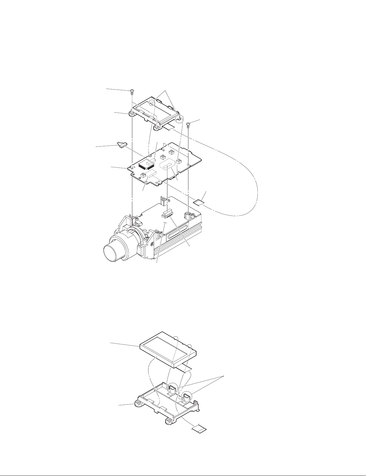
1-3-2. CPU-458 Board
Workflow: Lower case (P03)/upper case assembly (P03)/case (P03) (Section 1-3-1) → CPU-458 board
2 Two screws
(BTP1.7 x 6)
7 LCD frame (P03)
4 Harness
3 CPU-458 board
6 Two hooks
1 Two screws
(BTP1.7 x 6)
CN102
CN403
5 Flexible wiring board
CN401
CN502
RF-164 board
1-3-3. LCD Module
Workflow: Lower case (P03)/upper case assembly (P03)/case (P03) (Section 1-3-1) → CPU-458 board
(Section 1-3-2) → LCD module
3 LCD module
1 Two hooks
2 LCD frame (P03)
UTX-P03
1-3 (E)
Page 10

1-3-4. RF-164 Board
Workflow: Lower case (P03)/upper case assembly (P03)/case (P03) (Section 1-3-1) → CPU-458 board
(Section 1-3-2) → RF-164 Board
n
When attaching the screw, make sure that it is not loose.
3 RF lug (P03)
2 Screw
(P1.7 x 1.8)
1 Solder
5 RF-164 board
n
When attaching the RF lug (P03), make sure that the solder
portion of the RF lug (P03) terminal portion is not raised and
that the land portion of the board is not removed.
6 Harness
When attaching, route the lead wires of the battery
plate (P03) assembly along the groove as shown
in the illustration, and retain them with the earth
plate (P03).
7 Earth plate (P03)
Lead wire (black)
CN501
2 Screw
(P1.7 x 1.8)
3 RF lug (P03)
4 Four screws
(BTP1.7 x 6)
5 RF-164 board
7 Earth plate (P03)
1-4 (E)
Lead wire (red) Lead wire (orange)
Boss
8 Battery plate (P03) assembly
UTX-P03
Page 11

1-3-5. XLA Connector Assembly
Workflow: Lower case (P03)/upper case assembly (P03)/case (P03) (Section 1-3-1) → CPU-458 board
(Section 1-3-2) → RF-164 Board (Section 1-3-4) → XLA connector assembly
Removal procedure
Remove the hook by rotating the connector assembly (P03)
in the direction of the arrow B, then remove it in the
direction of the arrow C.
B
Connector assembly (P03)
C
Hook
7 XLA connector assembly
Installation procedure
Compress the coil spring by pushing the ring (P03) in the
direction of the arrow D, then attach the connector
assembly (P03) in the direction of the arrow E.
n
Check that the hook is hooked on the chassis.
Coil spring
E
D
Connector assembly (P03)
Ring (P03)
Hook
Chassis
4 Connector holder
Hook
6 Remove the coil spring while
pushing the latch portion in the
direction of the arrow A.
5 Ring (P03)
Latch
3 Screw
(P2 x 7)
A
2 Screw
(P2 x 7)
1 Two screws
(P2 x 7)
UTX-P03
1-5 (E)
Page 12

1-4. Diagnosis of Failure
When replacing the parts or boards, perform the operation check of this unit. (Refer to Section 2.)
1-4-1. No Sound is Output/Service Area is Narrow/There is a Noise
Sound is output with
strong radio wave.
Check the receiver.
Symptom pointed out: . No sound is output.
Perform the check using the checking
receiver (URX-P03).
Sound is output with
weak radio wave.
. Service area is narrow.
. There is a noise.
No sound is output
(there is a noise) with
strong radio wave.
The “COMPANDER”
setting is not correct.
(Change the setting
according to the
receiver type to be
used.)
Check the connected
microphone unit.
No sound is output
(there is a noise) with
weak radio wave.
. Check the destination.
(Are the destinations
of receiver and
transmitter correct?)
. Check the transmission
channel. (Does it match
with the reception
channel?)
Change RF POWER
(transmission output
level) from “L” to “H”.
Check the connection
of FFC and harness,
and the connector.
t
FFC: Flexible flat cable
Check the disconnection
of RF lug (P03), and
replace it as required.
(Refer to Section 1-3-4.)
t
The possible causes of the RF lug (P03) disconnection are
as follows. (Refer to Section 1-3-4.)
. Screw is loose.
. Solder is raised.
. Land is
1-4-2. Sound is distorted
1-6 (E)
RF-164 board failure.
Replace the RF-164
board. (Refer to Section
1-3-4.)
Symptom pointed out: Sound is distorted.
The setting of ATT (attenuator) is not correct.
Change the setting of ATT so that the audio indicator blinks in green.
→
The setting of IN LEVEL (audio input level) is not correct.
Change it to the appropriate setting (MIC or LINE).
→
CPU-458 board failure.
Replace the CPU-458
board. (Refer to Section
1-3-2.)
UTX-P03
Page 13

1-5. Lead-free Solder
All boards mounted in this unit use lead-free solder. Be sure to use lead-free solder when repairing the
boards of this unit. A lead free mark (LF) indicating that the solder contains no lead is printed on each
board.
(Caution: Some printed circuit boards may not come printed with the lead free mark due to their particular
size.)
: LEAD FREE MARK
n
. The lead-free solder melts at a temperature about 40 dC higher than the ordinary solder, therefore, it is
recommended to use the soldering iron having a temperature regulator.
. The ordinary soldering iron can be used but the iron tip has to be applied to the solder joint for a slightly
longer time. The printed pattern (copper foil) may peel away if the heated tip is applied for too long, so
be careful.
UTX-P03
1-7 (E)
Page 14

Page 15

Section 2
Operation Check
When replacing the parts or boards, perform the operation check of this unit.
2-1. Preparation
2-1-1. Required Equipment
Name Specification Device name
Spectrum analyzer Frequency: 10 kHz to 3 GHz Advantest R3371B or the equivalent
Audio analyzer . Analog input Audio Precision system2 or the equivalent
. Frequency range: 20 to 100 kHz
Tester
2-1-2. Tool List
Name Specification Device name/part number
Checking receiver _ URX-P03 (works properly)
Checking transmitter _ UTX-P03 (works properly)
(for comparison)
Measuring antenna _ 1-501-952-22
Measuring cable XLR (female) - XLR (male) Optional accessory
Measuring cable BMP-XLR (male) 1-792-249-23
Headphone Stereo mini-jack Optional accessory
Dynamic microphone _ F-780 or the equivalent
UTX-P03
2-1 (E)
Page 16

2-2. Check of Transmission Output
2-2-1. Required Equipment/Tool
. Spectrum analyzer
. Measuring antenna
2-2-2. Setting
Set the transmission frequency, transmission level and spectrum analyzer of this unit.
1. Transmission frequency
Destination Channel Frequency
U14 1601 482.125
U30 3201 578.125
U42 4401 650.125
CE21 2233 482.125
CE33 3433 578.125
CE42 4333 650.125
CE51 5233 722.125
KR 50 931.250
E 6901 800.125
2. Transmission level
Transmission level: H
3. Spectrum analyzer
. Center Frequency: Set according to “1. Transmission frequency”.
. Reference Level: 20 dBm
. Frequency Span: 200 kHz
. RBW: Auto
. VBW: Auto
. ATT: Auto
2-2 (E)
UTX-P03
Page 17

2-2-3. Procedure
1. Connect the measuring antenna to the RF input of the spectrum analyzer.
2. Connect the dynamic microphone to this unit.
Spectrum analyzer
Dynamic microphone
Antenna
3. Check the transmission output level by bringing the antenna portion of the transmitter into contact
with the measuring antenna.
t
Perform the measurement while holding the dynamic microphone.
Specification: 0 dBm or more
20 dBm
0 dBm or more
v:10 dB/div
H:20 kHz/div
UTX-P03
2-3 (E)
Page 18

2-3. Check of Sound Output
2-3-1. Required Equipment/Tool
. Audio analyzer
. Checking receiver
. Headphone
. Microphone for transmitter
2-3-2. Setting
1. Set this unit by referring to Section 2-2-2.
2-3-3. Procedure
1. Set the channels of this unit and the checking receiver so that they match each other.
2. Make a voice toward the microphone, and check the sound with the headphone output of the checking
receiver.
3. Tap this unit lightly, and check the following.
. Sound can be heard clearly.
. Noise is not mixed.
. Sound is not interrupted.
. Audio input level meter is displayed in accordance with the sound.
2-4 (E)
UTX-P03
Page 19

2-4. Check of Sound Level
2-4-1. Required Equipment/Tool
. Audio analyzer
. Checking receiver
. Measuring cable BMP-XLR (male/female)
. Measuring cable XLR (female) - XLR (male)
2-4-2. Setting
. Transmitter (UTX-P03)
Transmission channel (GP/CH): Refer to “1. Transmission frequency” in Section 2-2-2.
Transmission level (RF POWER): H
Sound attenuator level (ATT): 0
Sound input level (IN LEVEL): MIC
. Receiver
Sound output level (OUTPUT LEVEL): 0
. Audio analyzer
Output: Level (_60 dBV)
Frequency (1 kHz)
Input: Filter (A-weighted)
2-4-3. Procedure
1. Connect each device according to the following illustration.
Measuring cable
XLR (female) – XLR (female)
Audio analyzer
Transmitter Receiver
Measuring cable
BMP-XLR (male)
2. Check the sound output level of this unit with the audio analyzer.
Specification:
Sound output level from the receiver: _60 dBV ?3 dB
UTX-P03
2-5 (E)
Page 20

2-5. Check of +48V
2-5-1. Required Equipment/Tool
. Tester
2-5-2. Procedure
1. Set “IN LEVEL” to “MIC” with the operation menu of this unit.
2. Set “+48 V” to “ON” with the operation menu of the main unit.
3. Measure the voltage between No.1 (minus) and No.2 (plus) of the Audio Input connector.
Specification: 43 ?3 V
2
1
3
Audio Input connector
2-6 (E)
UTX-P03
Page 21

Section 3
Spare Parts
3-1. Notes on Repair Parts
1. Safety Related Components Warning
w
Components marked ! are critical to safe operation.
Therefore, specified parts should be used in the case of
replacement.
2. Standardization of Parts
Some repair parts supplied by Sony differ from those
used for the unit. These are because of parts commonality and improvement.
3. Stock of Parts
Parts marked with “o” at SP (Supply Code) column of
the spare parts list may not be stocked. Therefore, the
delivery date will be delayed.
4. Harness
Harnesses with no part number are not registered as
spare parts.
3-1. 補修部品注意事項
1. 安全重要部品
! 警告
! 印のついた部品は安全性を維持するために重要
な部品です。したがって,交換する時は必ず指定
の部品を使ってください。
2. 部品の共通化
ソニーから供給する補修用部品は,セットに使われて
いるものと異なることがあります。
これは部品の共通化,改良等によるものです。
3. 部品の在庫
部品表の SP(Supplycode)欄に“o”で示される部品は
在庫していないことがあり,納期が長くなることがあ
ります。
4. ハーネス
部品番号の記載されていないハーネスは,サービス部
品として登録されていません。
UTX-P03
3-1
Page 22

Case
3-2. Exploded Views
6
5
4
8
P2 x 8
1
7
3
8
2
No. Part No. SP Description
1 A-1901-011-A s BATTERY CASE (B) ASSY
2 A-2015-557-A s PLATE (P03) ASSY, BATTERY
3 X-2589-603-1 s UPPER CASE ASSY (P03)
4 4-527-780-01 s CASE (P03)
5 4-527-782-01 s BUTTON (P03), SET
6 4-527-783-01 s WINDOW (P03)
7 4-527-785-01 s CASE (P03), LOWER
8 4-645-214-72 s GRIP, M2
7-685-105-19 s SCREW +P 2X8 TYPE2 NON-SLIT
3-2
UTX-P03
Page 23

No. Part No. SP Description
101 A-2015-418-A s MOUNTED CIRCUIT BOARD, CPU-458
102 A-2015-423-A s MOUNTED CIRCUIT BOARD, RF-164 (UC14)
A-2015-424-A s MOUNTED CIRCUIT BOARD, RF-164 (UC30)
A-2015-425-A s MOUNTED CIRCUIT BOARD, RF-164 (UC42)
A-2015-426-A s MOUNTED CIRCUIT BOARD, RF-164 (CE21)
A-2015-427-A s MOUNTED CIRCUIT BOARD, RF-164 (CE33)
A-2015-428-A s MOUNTED CIRCUIT BOARD, RF-164 (CE42)
A-2015-429-A s MOUNTED CIRCUIT BOARD, RF-164 (CE51)
A-2015-632-A s MOUNTED CIRCUIT BOARD, RF-164 (E)
A-2042-774-A s MOUNTED CIRCUIT BOARD, RF-164 (KR)
103 A-2015-556-A s CONNECTOR ASSY (P03)
104 1-811-964-11 s LCD MODULE
105
105 3-318-203-11 s SCREW (B1.7X6), TAPPING
106 4-527-787-01 s LUG (P03), RF
7-627-553-88 s SCREW,PRECISION +P 2X7
7-627-852-37 s PRECISION SCREW +P1.7X1.8TYPE3
101
Chassis
104
105
103
P2 x 7
P1.7 x 1.8
105
106
102
UTX-P03
P2 x 7
P2 x 7
3-3
Page 24

3-3. Electrical Parts List
------------CPU-458 BOARD
------------ Ref. No.
or Q'ty Part No. SP Description
1pc A-2015-418-A s MOUNTED CIRCUIT BOARD, CPU-458
3-4. Packing Materials & Supplied
Accessories
---------------------------------------PACKING MATERIALS & SUPPLIED ACCESSORIES
--------------------------------------- Ref. No.
or Q'ty Part No. SP Description
1pc 2-693-884-11 s CASE, SOFT
1pc
!
4-530-734-01 s CD-ROM (INSTRUCTION MANUAL)
MANUAL (PDF), INSTRUCTION
-----------RF-164 BOARD
----------- Ref. No.
or Q'ty Part No. SP Description
1pc A-2015-423-A s MOUNTED CIRCUIT BOARD, RF-164 (UC14)
A-2015-424-A s MOUNTED CIRCUIT BOARD, RF-164 (UC30)
A-2015-425-A s MOUNTED CIRCUIT BOARD, RF-164 (UC42)
A-2015-426-A s MOUNTED CIRCUIT BOARD, RF-164 (CE21)
A-2015-427-A s MOUNTED CIRCUIT BOARD, RF-164 (CE33)
A-2015-428-A s MOUNTED CIRCUIT BOARD, RF-164 (CE42)
A-2015-429-A s MOUNTED CIRCUIT BOARD, RF-164 (CE51)
A-2015-632-A s MOUNTED CIRCUIT BOARD, RF-164 (E)
A-2042-774-A s MOUNTED CIRCUIT BOARD, RF-164 (KR)
QUICK START GUIDE(PDF)
FREQUENCY LIST (PDF)
(JAPANESE, ENGLISH, FRENCH,
GERMAN, ITALIAN, SPANISH, KOREAN,
TURKISH)
3-4
UTX-P03
Page 25

Section 4
Block Diagrams
4-1. Circuit Description
4-1-1. RF-164 Board
The RF-164 board consists of the following:
1. Audio circuit
2. Radio frequency circuit
1. Audio circuit
An audio signal is input from CN501. Power (48 VDC) for microphone phantom is supplied from
CN501. The phantom power is generated using a DC-DC converter (IC602) and ON/OFF-controlled
using CPU (IC404: CPU-458 board). The audio signal input from CN501 is selected as “LINE” or “MIC”
according to the input level using switches (PH501, PH502, and PH503). The audio signal selected on the
“LINE” side is attenuated by 24 dB using a resistance attenuator and input to a head amplifier (IC501).
The audio signal selected on the “MIC” side is input to a head amplifier (IC501).
The gain of the head amplifier is controlled by CPU (IC404: CPU-458 board). Gain setting can be selected in ten level using “AF ATT” in an operation menu (only during “MIC” selection). The audio signal
whose volume was controlled by gain setting is input to DSP (IC506). DSP processes a compander or
tone signal.
The compander or tone signal is selected using “COMPANDER” in an operation menu.
2. Radio frequency circuit
An oscillator circuit is based on a PLL frequency synthesizer system.
The audio signal that was processed using DSP is input through a low-pass filter (LPF) to VCO (VoltageControlled Oscillator) (VCO201) for modulation. The modulated audio signal is then processed as a radio
frequency (RF) signal.
The RF signal amplified using a radio frequency amplifier (consisting of Q204 and Q206) is adjusted in
an output level using IC205 and IC209 that are controlled by CPU, input to LPF and isolators (ISO201
and ISO202), and radiated from an antenna.
4-1-2. CPU-458 Board
The CPU-458 board consists of the following:
1. CPU
2. Power circuit
1. CPU
CPU (IC403) controls various functions of this unit.
. RF signal output level . LCD display . USB connection
. PLL . LED display . Current control
. DSP . Button operation . Charge control
. Audio signal level . Infrared operation . Remaining battery detection
. 48 VDC power control
The information below is recorded in EEPROM and controlled by CPU.
EEPROM1 (RF-164 board): . Electrical alignment information . Destination information
EEPROM2 (CPU-458 board): . Last memory . Software for main unit control
UTX-P03
4-1 (E)
Page 26

2. Power circuit
The power circuit of UTX-P03 has the four functions below.
(1) Driving by dry battery
(2) Driving by USB power
(3) Charging to nickel metal hydride by USB power
(4) Circuit power generation from various input power supplies
(1) Driving by dry battery
The power (3 VDC) input from a dry battery is supplied to DC-DC converters (IC107 and IC109) through
CN102.
(2) Driving by USB power
UTX-P03 can be operated by the power (+5 V) supplied from USB.
The power input from a USB terminal is generated as +3.65 V using a DC-DC converter (IC106) and
supplied from CN403 to an RF-163 board through a transistor switch (Q109). At that time, USB power is
selected when the voltage input from the USB terminal is detected by CPU (IC404). Power is switched to
the dry battery side when the power supply from the USB terminal is interrupted. (The USB power has
priority.)
(3) Charging to nickel metal hydride by USB power
The power (+5 V) input from a USB terminal is generated as +3.65 V using a DC-DC converter (IC106)
and input to a transistor switch (Q109). The voltage input from the USB terminal is detected using CPU
(IC404). It turns on a transistor switch (Q106) and supplies USB power to a charging control circuit
(IC108). In the charging control circuit (IC108), the internal resistance values of batteries are read from
the voltages of two batteries for charging control. The charging control circuit (IC108) controls Q111,
Q112, and Q113 to perform charging.
(4) Circuit power generation from various input power supplies
A circuit power of +3.3 V and +5.5 V is generated from various input power supplies.
Various power supplies selected using Q101, Q104, and Q109 generate +3.3 V in a DC-DC converter
(IC107) and generate +5.5 V in IC109. The circuit power is supplied from CN403 to an RF-164 board.
4-2 (E)
UTX-P03
Page 27

4-2. Overall Block Diagrams
OverallOverall
XLA 3P
CN-3708
RF-164
CN501
IC602
+5.5V
48V
DDC
+48V
48V_SHDN
48V_LOAD
to CPU
PH501
PH502
PH503
LINE
ATT
MIC
24 dB
IC602
+5V
REG
IC501
IC503
GAIN
CONTROL
+5.0V
HEAD
AMP
AF ATT
to CPU
IC506
X501
TCXO
26 MHz
DSP
DSP
to CPU
MOD
LPF
IC203
ACTIVE
LOOP FILTER
X201
TCXO
19.2 MHz
IC204
VCO201
IC201
+5.5V
+5 V
REG
+5.0V
VCO
Vt
LOOP
FILTER
PLL
Q202
+3.3V
Q204
IC209
DIGITAL
POTENTIOMETER
Q206
RF ADJ (2)
PLL
IC205
RF POWER ADJ
RF ADJ (1)
*1
ISO201: UC14. CE21
ISO202: UC30, UC42, CE33, CE42, CE51
*1
ISO201
ISO202
LPF
ISOLATOR
J201
RF TEST
POINT
DC 3 V
CHARGE
VOLTAGE
CHECK
MicroUSB
CPU-458
CN102
CN101
Q101, Q104
Q106
Q112
Q113
BATT
CHECK
to CPU
IC108
BATTERY
CHARGE
CONTROLER
Q111
CONSTUNT
CURRENT
FET
IC106
+3.65 V
DDC
IC101
USBUART
Q109
IC107
+3.3 V
DDC
IC109
+5.5 V
DDC
CPU
+3.3 V
Q114
+3.3 V
+5.5 V
AF ATT
from IC503
DSP
from IC506
POWER
CHARGE LED
BATT
CHECK
from CN102
USB POWER DETECT
USB FIRMWARE WRITING
CPU
CN502
CN403
IC404
48V_SHDN
48V_LOAD
from IC602
IC208
EEPROM1
EEPROM2
TACT SW
IR
RECEIVER
IC402
LED
CN401
LCD
Overall
UTX-P03
4-3
4-3
Page 28

4-3. Frame Wiring
CONNECTOR ASSEMBLY (P03)
XLA 3P
Frame WiringFrame Wiring
RF-164
CN-3708
DC 3 V
CN501
1HOT
COLD
2
GND
3
CPU-458
CN102
1 BATT_
NC
2
NC
3
BATT+/_
4
NC5
NC6
BATT+7
CN101
CN502
CN403
J201
CN401
RF TEST
POINT
LCD
MicroUSB
Frame Wiring
4-4
4-4
UTX-P03
Page 29

Page 30

UTX-P03 (CE)
UTX-P03 (E)
UTX-P03 (KR)
UTX-P03 (UC) J, E
9-878-548-01
Sony Corporation
Printed in Japan
2014. 1 08
©2014
 Loading...