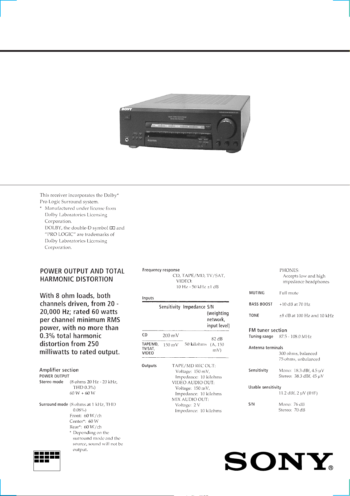
STR-V220
SERVICE MANUAL
US Model
SPECIFICATIONS
FM STEREO/FM-AM RECEIVER
— Continued on next page —
MICROFILM
– 1 –
SAFETY CHECK-OUT
After correcting the original service problem, perform the following safety checks before releasing the set to the customer:
Check the antenna terminals, metal trim, “metallized” knobs, screws,
and all other exposed metal parts for A C leakage. Check leakage as
described below.
LEAKAGE
The AC leakage from any exposed metal part to earth Ground and
from all exposed metal parts to any exposed metal part having a
return to chassis, must not exceed 0.5 mA (500 microampers). Leakage current can be measured by any one of three methods.
1. A commercial leakage tester, such as the Simpson 229 or RCA
WT-540A. Follow the manufacturers’ instructions to use these
instruments.
2. A battery-operated AC milliammeter. The Data Precision 245
digital multimeter is suitable for this job.
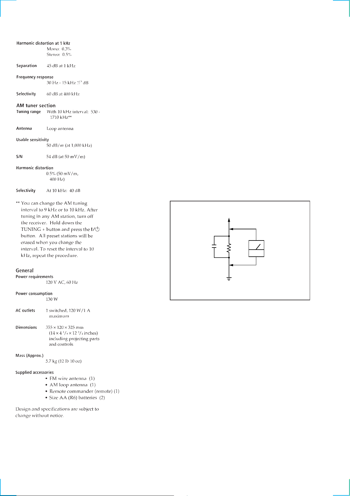
3. Measuring the voltage drop across a resistor by means of a V OM
or battery-operated AC voltmeter . The “limit” indication is 0.75
V, so analog meters must have an accurate low-voltage scale.
The Simpson 250 and Sanwa SH-63Trd are examples of a passive VOM that is suitable. Nearly all battery operated digital
multimeters that have a 2V AC range are suitable. (See Fig. A)
To Exposed Metal
Parts on Set
0.15µF
1.5k
Earth Ground
Ω
AC
voltmeter
(0.75V)
Fig. A. Using an AC voltmeter to check AC leakage.
Notes on chip component replacement
• Never reuse a disconnected chip component.
• Notice that the minus side of a tantalum capacitor may be
damaged by heat.
SAFETY-RELATED COMPONENT WARNING !!
COMPONENTS IDENTIFIED BY MARK ! OR DO TTED LINE
WITH MARK ! ON THE SCHEMATIC DIAGRAMS AND IN
THE PARTS LIST ARE CRITICAL TO SAFE OPERATION.
REPLACE THESE COMPONENTS WITH SONY PARTS
WHOSE PART NUMBERS APPEAR AS SHOWN IN THIS
MANUAL OR IN SUPPLEMENTS PUBLISHED BY SONY.
– 2 –

TABLE OF CONTENTS
1. SERVICING NOTE .......................................................... 3
2. GENERAL .......................................................................... 4
3. ELECTRICAL BLOCK CHECKING...................... 5
4. DIAGRAMS
4-1. Circuit Boards Location........................................................ 6
4-2. Schematic Diagram – Main (1/3) Section –.......................... 7
4-3. Schematic Diagram – Main (2/3) Section –.......................... 9
4-4. Schematic Diagram – Main (3/3) Section –........................ 11
4-5. Printed Wiring Board – Main Section – .............................. 13
SECTION 1
SERVICING NOTE
4-6. Printed Wiring Board – Display Section –.......................... 15
4-7. Schematic Diagram – Display Section – ............................ 17
4-8. Schematic Diagram – Panel Section – ................................ 19
4-9. Printed Wiring Board – Panel Section –.............................. 21
4-10. IC Block Diagrams ........................................................... 23
4-11. IC Pin Functions ............................................................... 26
5. EXPLODED VIEWS
5-1. Case Section........................................................................ 28
5-2. Chassis Section ...................................................................29
6. ELECTRICAL PARTS LIST ........................................30
FACTORY SET
Mode which sets the preset settings of the unit to that at shipment.
Procedure:
While pressing the VIDEO button and TV/SAT button together, press the 1/u button to turn on the power.
“FACTORY” will be displayed and factory settings executed.
INITIALIZATION
Mode which erases all the preset settings of the unit.
Use this mode when returning the unit to the customer.
Procedure:
While pressing the VIDEO button, TV/SAT button, and TAPE/MD button together, press the 1/u button to turn on the power.
“INITIAL” will be displayed and initialization executed.
FLUORESCENT INDICATOR TUBE LIGHTING CHECK
Mode which lights up the whole fluorescent indicator tube or partially.
Procedure:
While pressing the TV/SAT button and TAPE/MD button together, press the 1/u button to turn on the power.
The fluorescent indicator tube will light up in about 0.5 seconds, and then start to light up partially. After partial lighting completes, the
BASS BOOST indicator will light up, “FINISH” will be displayed, indicating that fluorescent indicator tube lighting check has completed.
SWITCHING OF 9 kHz/10 kHz AM CHANNEL STEP
The AM channels of this unit can be switched between 9 kHz and 10 kHz.
Procedure:
Set FUNCTION to AM and turn off the power.
While pressing the TUNING + button, press the 1/u button to turn on the power.
“9 k STEP” or “10 k STEP” will be displayed, and the channel step will be switched.
– 3 –
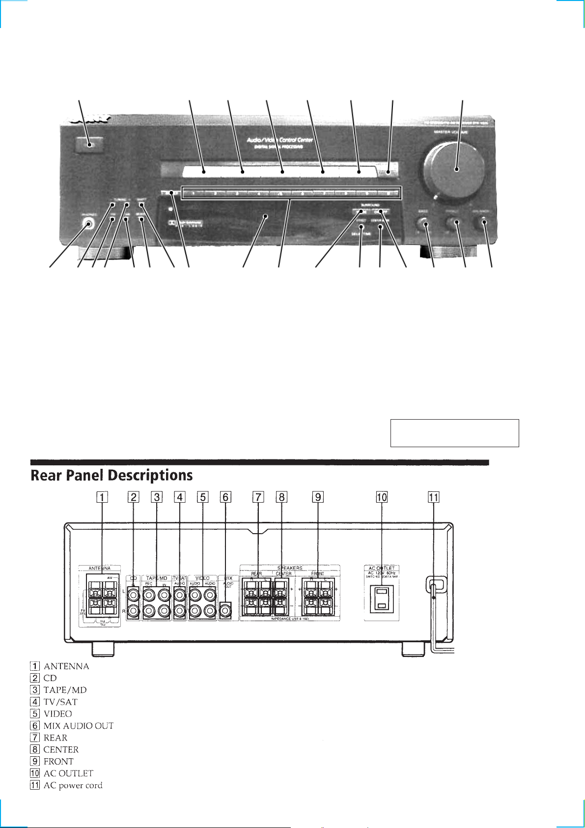
Front Panel Descriptions
SECTION 2
GENERAL
1
20
25
24
Location of Parts and Controls
1 1/u button
2 VIDEO button
3 TV/SAT button
4 TAPE/MD button
5 CD button
6 TUNER button
7 BASS BOOST indicator
8 MASTER VOLUME knob
9 BALANCE knob
212223
3
19
10 TREBLE knob
11 BASS knob
12 SURROUND ON/OFF button
13 CENTER MODE button
14 EFFECT/DELA Y TIME button
15 SURROUND MODE button
16 Numeral (1 to 0) button
17 Display window
18 DIRECT button
46
5
1617 1011131415
782
12
19 SHIFT button
20 MEMORY button
21 AM button
22 TUNING + button
23 FM button
24 TUNING – button
25 PHONES jack
918
This section is extracted from
instruction manual.
– 4 –
SECTION 3
ELECTRICAL BLOCK CHECKING
STR-V220
SECTION 4
DIAGRAMS
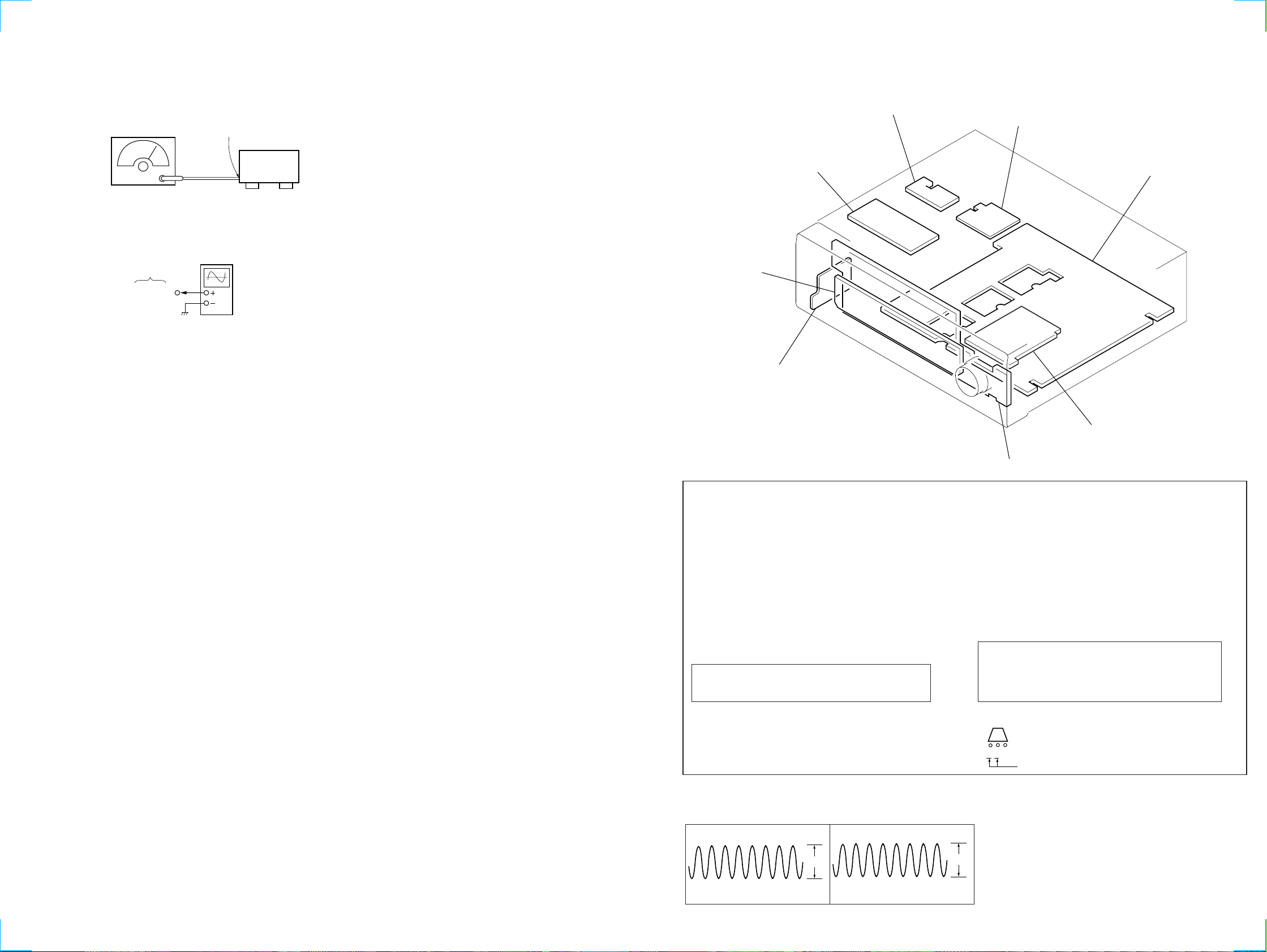
ADJUSTING THE FM/SD SIGNAL SENSITIVITY
Setting:
FM RF SSG
Carrier frequency: 98 MHz
Modulation: AUDIO 1 kHz,
Output level: 26 dB (at 75
Main board
TP (IC501
6
pin)
Procedure:
1. Set the SSG output level to 26 dB and input the signal.
2. Adjust SFR501 so that the oscilloscope level becomes 0V.
3. Raise the SSG output level slightly (max. 35 dB) when the adjustment in step 2 fails, and repeat steps 1 and 2.
NOTE: If the adjustment cannot be performed even when set to 35
dB, the sensitivity may be faulty, etc. Check the antenna
terminal connection, FM front end and IF circuit, etc. and
perform adjustments again.
FM ANTENNA (75Ω)
75 kHz deviation (100%)
Ω
open) (MAX 35 dB)
oscilloscope
Set
4-1. CIRCUIT BOARDS LOCATION
SECONDARY board
PRIMARY board
KEY board
PHONE JACK board
STANDBY board
MAIN board
VOL-TONE board
THIS NOTE IS COMMON FOR PRINTED WIRING
BOARDS AND SCHEMATIC DIAGRAMS.
(In addition to this, the necessary note is printed
in each block.)
For schematic diagrams.
Note:
• All capacitors are in µF unless otherwise noted. pF: µµF
50 WV or less are not indicated except for electrolytics
and tantalums.
• All resistors are in Ω and 1/
specified.
¢
•
• 2 : nonflammable resistor.
• C : panel designation.
Note: The components identified by mark ! or dotted line
• U : B+ Line.
• V : B– Line.
• Voltages and waveforms are dc with respect to ground
: internal component.
with mark ! are critical for safety.
Replace only with part number specified.
under no-signal (detuned) conditions.
no mark : FM
4
W or less unless otherwise
DISPLAY board
• Voltages are taken with a VOM (Input impedance 10 MΩ).
Voltage variations may be noted due to normal production tolerances.
• Waveforms are taken with a oscilloscope.
Voltage variations may be noted due to normal production tolerances.
• Circled numbers refer to waveforms.
• Signal path.
F : FM
For printed wiring boards.
Note:
• X : parts extracted from the component side.
• b : Pattern of the conductor side.
Caution:
Pattern face side: Parts on the pattern face side seen from
(Conductor Side) the pattern face are indicated.
Parts face side: Parts on the parts face side seen from
(Component Side) the parts face are indicated.
• Indication of transistor
C
EB
These are omitted
– 5 –
WA VEFORMS
MAIN (1/3) SECTION
1
8MHz
IC301 #™
DISPLAY SECTION
2
4.8Vp-p
5.4Vp-p
4.19MHz
IC201 #¢ X1
– 6 –
STR-V220
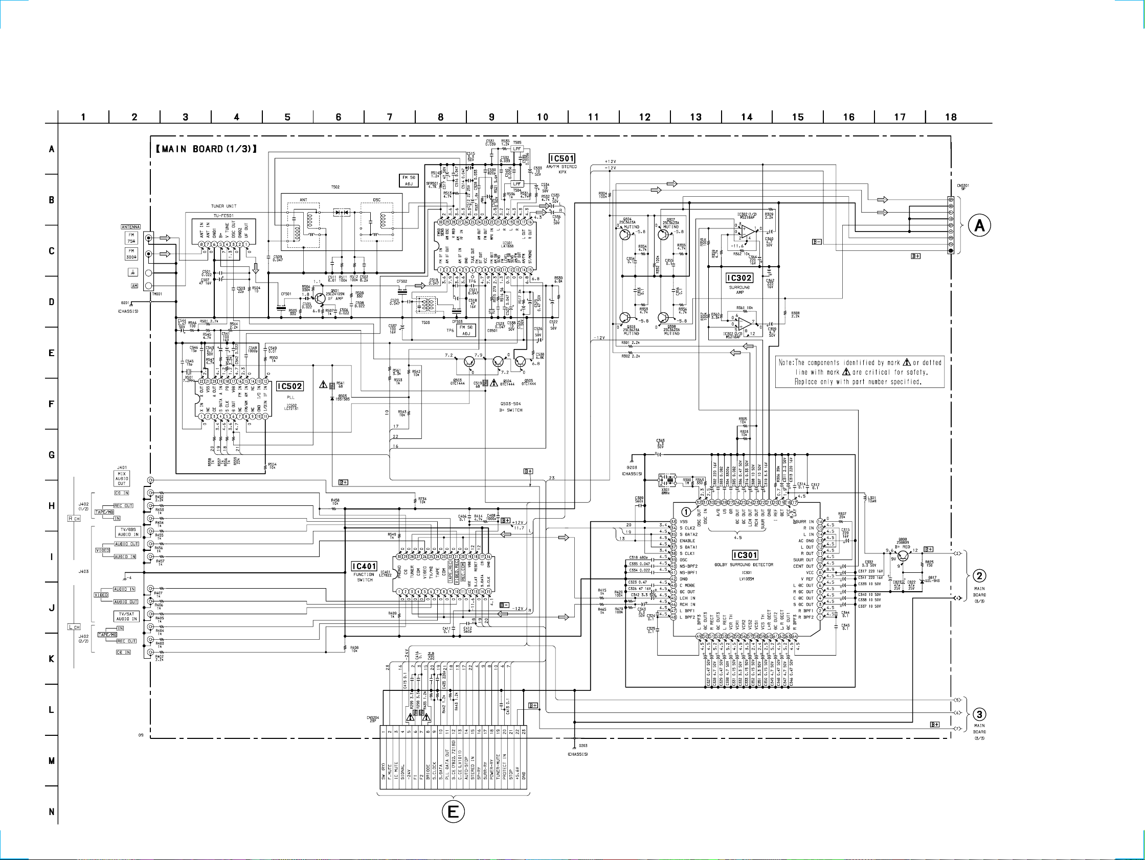
4-2. SCHEMATIC DIAGRAM – MAIN (1/3) SECTION –
• See page 6 for Waveforms.
• See page 13 for Printed Wiring Board.
• See page 23 for IC Block Diagrams.
(Page 19)
– 7 –
(Page 11)
(Page 11)
(Page 17)
– 8 –
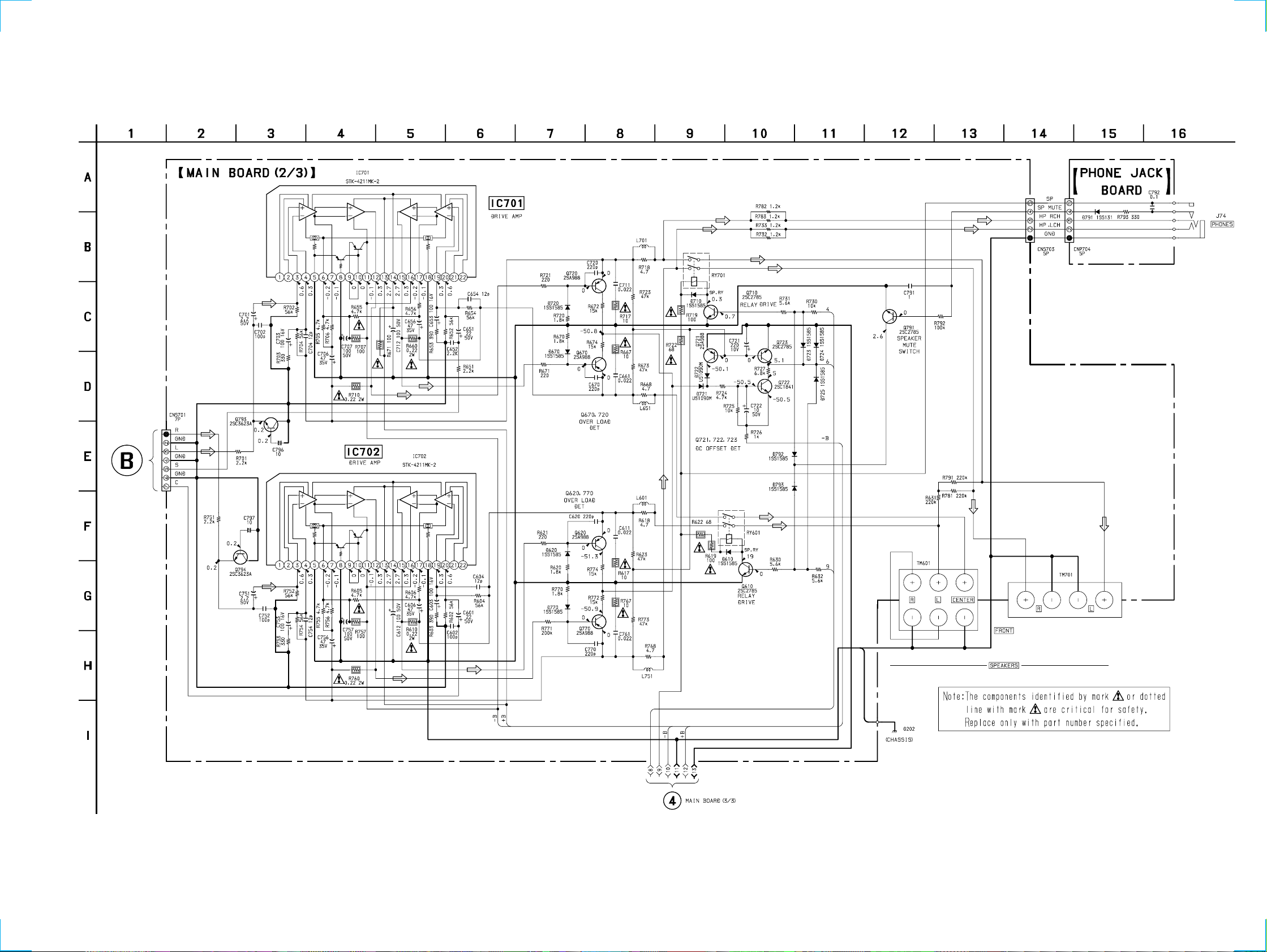
4-3. SCHEMATIC DIAGRAM – MAIN (2/3) SECTION –
• See page 13 for Printed Wiring Board.
STR-V220
(Page 20)
– 9 –
(Page 11)
– 10 –
STR-V220
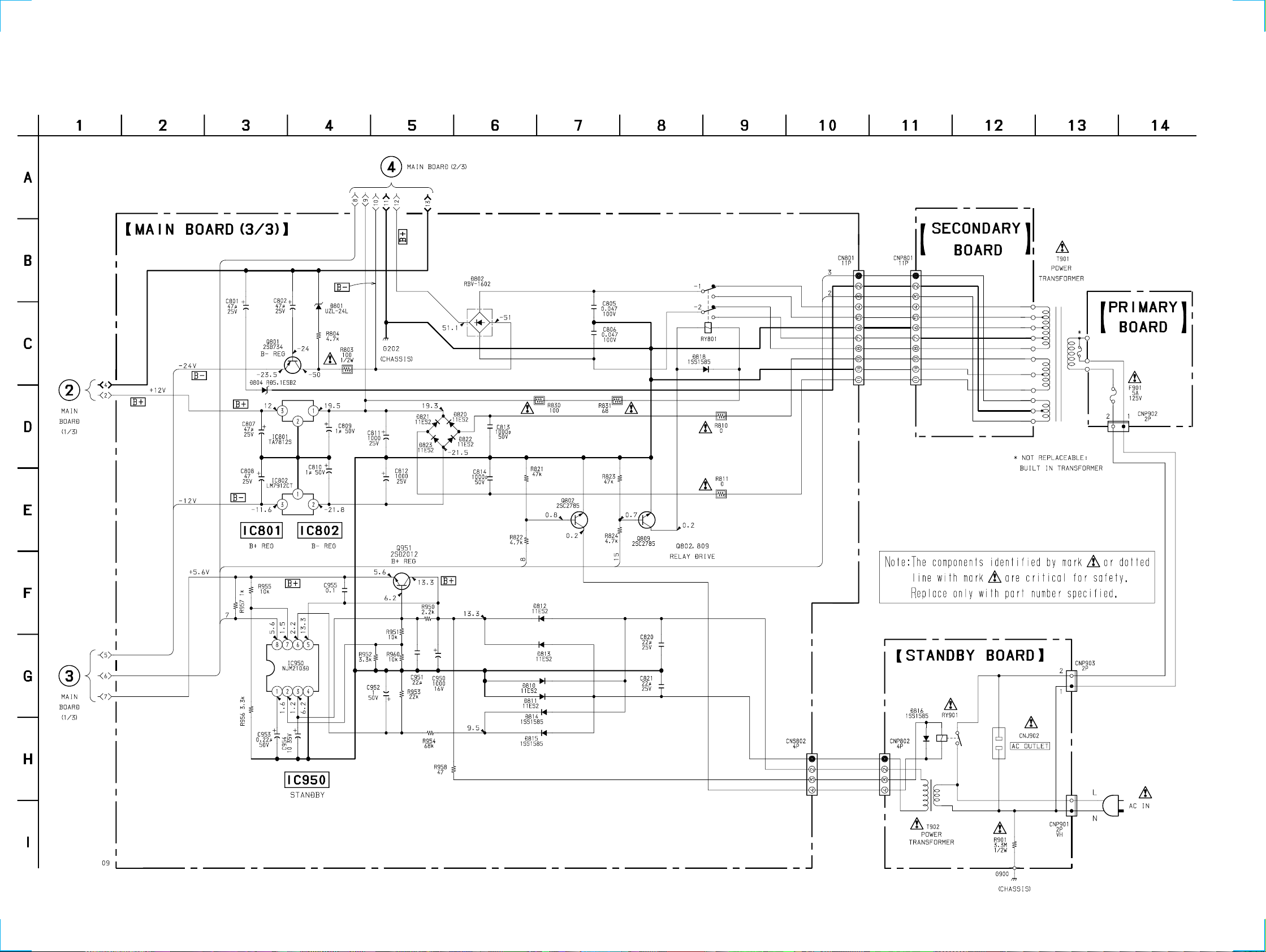
4-4. SCHEMATIC DIAGRAM – MAIN (3/3) SECTION –
• See page 24 for IC Block Diagrams.
(Page 9, 10)
(Page 8)
(Page 8)
– 11 –
– 12 –
JW297
SONY
PHONE JACK
1-673-706-11
J741
15
R793
1-673-706-
D791
C792
CNP702
VMRL B
4
11
(11)
PHONE
JACK
PHONE JACK BOARD
09
12
A
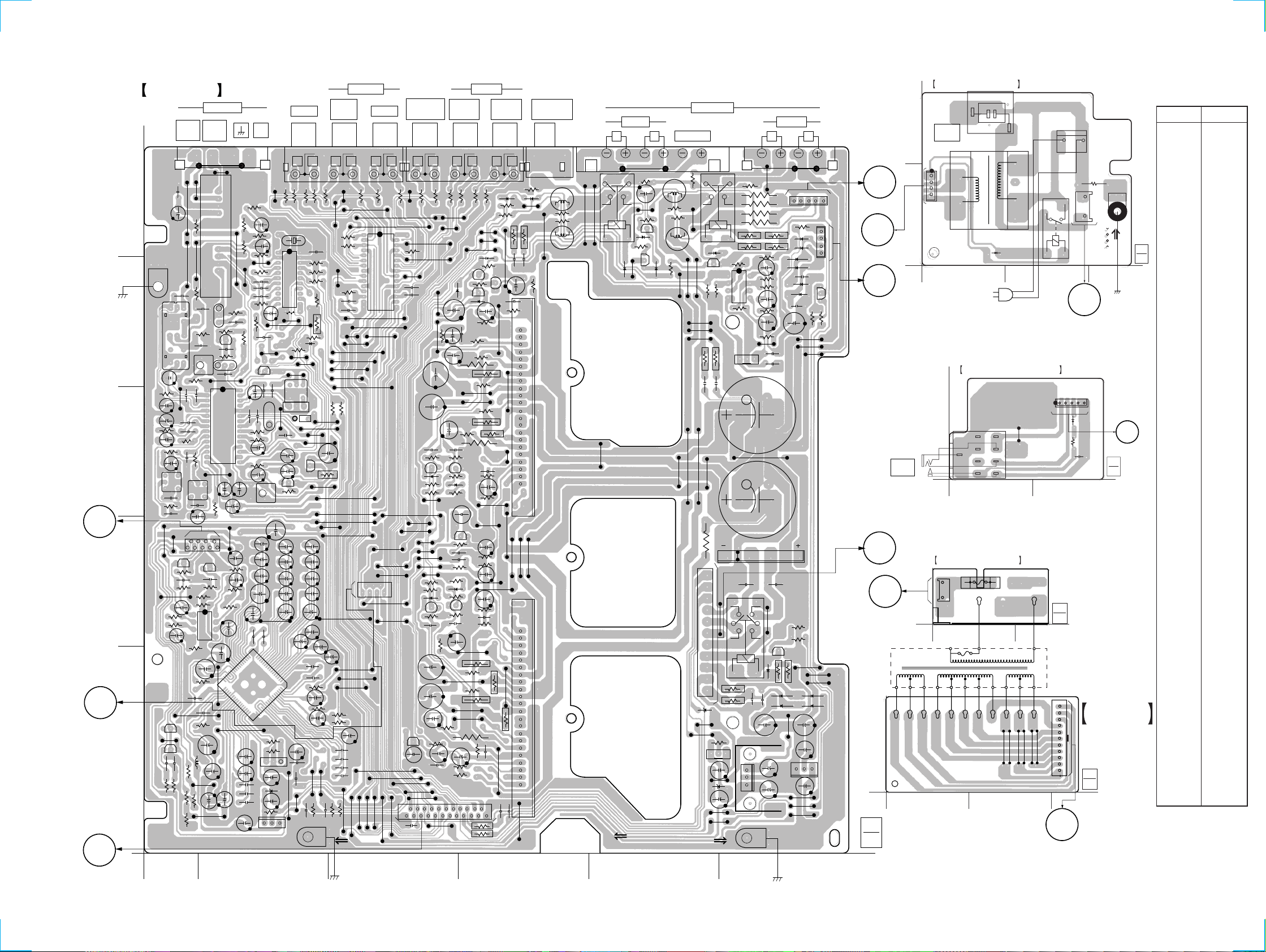
4-5. PRINTED WIRING BOARD – MAIN SECTION –
• See page 6 for Circuit Boards Location.
MAIN BOARD
ANTENNA
FM
A
(Page
21)
B
(Page
21)
C
(Page
15)
A
(CHASSIS)
B
C
D
E
09
TM001
C501
C507
G201
C509
T502
OSC ANT
C517
R513
C512 C515
R537
R529
R531
C533
T505
C539
R535
C531
JW249
JW248
Q307
R308
C355
R355
JW243
C359
R361
R360
C310
Q304
E
JW239
Q303
E
C354
R354
FM
300Ω
JW261
JW268
R504
JW266
JW259
R511
C511
R512
C502
SFR501
R514
C514
JW251
C530
C528
R521
C532
R536
T504
C540
CNS301
8
9
E
R356
8
5
IC302
R357
C315
R307
C314
C312
JW238
R306
R301
C353
JW236
R353
R302
R303
ANT
ANT
GND
UCC
FE501
OSC
GND
30
C516
16
C534
Q308
L301
C307
R305
JW235
UT
IC501
R352
R304
C311
75Ω
JW269
JW257
IF OUT
CF501
JW250
R532
C356
1
4
Q501
C508
JW256
C536
2
1
E
33
JW240
32
C313
C308
R359
C322
C535
C306
C316
R505
C505
R506
E
C522
R362
C317
JW237
JW263
C506
R507
CF502
C538
C525
JW247
C304
C303
C823
R544
R501
JW265
R508
C518
1
CD501
C521
15
R309
C360
48 49
C305
R546
C543
JW262
R548
C542
C503
C548
R549
C541
R550
R515
R516
R517
C302
R825
AM
C544
R547
C549
JW253
Q503
C523
SFR502
C339
C344
1617
CX301
D817
C822
B
Q808
JW264
R545
E
C519
C526
C524
Q505
C362
C338
C340
C341
JW244
C345
IC301
R363
R300
CE
STR-V220
STANDBY BOARD
A
AC
OUTLET
1
4
B
CNP802
09
PRIMARY BOARD
CNP902
NL
A
09
SONY
SECONDARY
1-673-707-11
1
– 14 –
CNJ902
T902
POWER TRANSFORMER
D816
1
AC
IN
F901
1
1-673-708-11
1-673-708-
JW295
2
SONY
1-673-705-11
STANDBY
CNP901
N
L
R901
N
RY901
1-673-705-
23
2
SONY
PRIMARY
11
(11)
2
TP901
POWER
TRANSFORMER
JW293
JW291
JW292
JW290
JW294
1-073-707-
11
CNP801
1
SECONDARY
11
(11)
3
3
G900
CNP903
(CHASSIS)
BOARD
R456
JW175
C601
R601
C770C620
D770
R770
C752
C652
R651
Q670
R660
R721
R710
AUDIO
OUT
J403
R406
D721
C606
R610
C797
R670
C670
R671
JW145
C703
R299
R298
JW173
Q721
R727
D724
C602
R760
R756
Q770
EE
R772
C653
E
R673
JW162
JW169
JW142
R705
CNS204
LRLRLRLRLR
E
Q723
C603
JW165
JW160
E
R702
R703
VIDEO
R457
JW172
R724
R603
R602
R606
R621
R755
R704
R407
JW174
D722
E
R771
C754
R753
JW158
JW154
C751
JW149
2
R730
Q722
R605
R711
1
E
JW166
R754
R752
R652
JW148
R653
C654
R654
C704
AUDIO
IN
D723
R632
R617 R667
JW143
C604
R604
JW163
JW213
C753
C651
JW140
R707
JW139
C415
C722
IC702
R757
IC701
C416
MIX
AUDIO OUT
REAR
LR
L601
L651
R618
R668
TM601
JW135
JW134
JW119
JW138
C611
JW152
R734
D725
22
1
JW151
J253
JW170
C661
R725
JW150
RY601
D610
R630
JW131
JW133
R631
JW132
R792
D793
Q610
E
E
Q791
D792
L751
C791
L701
R768
R731
R718
CENTER
JW129
JW117
R781
JW130
JW128
JW126
JW125
JW124
JW116
1
SPEAKER
Q710
JW127
R957
R717
C711
JW115
JW118
R803
D710
R955
C761
C804
E
5
R767
R956
8
IC950
R732
R733
R782
R783
R951
E C B
JW112
R791
RY701
Q951
C805
FRONT
LRLR
JW123
JW122
15
R958
R622R619
R954
R719R772
C952C953
1
R952
R960
4
R953
C954
R950
JW114
C951
C955
JW113
S
S
C806
C950
C803
D811
D810
C821
D814
D815
D812
C820
D813
JW121
JW120
JW296
4
1
Q902
E
R822
R821
4
1
1
3
2
22
1
JW136
CN801
JW111
RY801
D804
JW110
JW109
C801
D801
C802
Q801
R804
CB
JW107
JW106
E
G202
R810
R811
C814
1
2
IC801
3
11
JW108
54321
JW105
Q809
D818
R831
D820
D821
C813
C809
C807
(CHASSIS)
R823
R824
E
R830
JW100
JW099
JW098
D822
D823
C812C811
JW104
C810
IC802
1
32
C808
JW103
JW102
JW101
1-673-709-
6
A
09
11
(11)
TAPE/MD
REC
ONT
INCD IN
TA/SAT
AUDIO IN
J402
JW270
R559
R541
JW214
JW190
JW234
R543
C327
R420
R442
R459
R460
JW230
JW221
JW220
JW219
R542
JW211
JW209
JW205
JW207
JW200
C318
C335
C334
C323
R441
R414
C408
C406
JW225
JW222
JW208
JW196
R415
JW224
JW223
JW188
JW197
JW189
R403
JW233
30
16
CNS701
6
7
C326
JW188
R453
R402
R408
R458
R452
X501
C545
1
22
12
IC502
JW218
C520
C527
JW258
JW229
JW252
R538
C350
C331
64
1
G203
R554
R561
E
C349
C348
C346
C342
C329
C343
JW194
11
JW254
TP6
Q504
R470
C309
JW192
JW255
C537
E
C330
C325
C324
C365
C363
C434
R558
R557
R556
T503
JW215
JW212
R465
C342
R435
D503
JW217
JW216
R519
C332
C333
C351
C352
C328
JW191
C435
JW228
JW227
JW183
R454
IC401
JW226
JW201
JW187
JW231
JW206
JW204
JW203
2
JW199
JW182
JW186
JW232
1
JW181
JW185
R404
1
15
JW184
23
JW242
JW171
C411
C412
JW278
22
C413
C612
C757
JW277
JW276
R672
R720
D720
Q720
C712
C707
C706
Q793
C796
JW180
JW179
R455
JW178
R410
JW177
R623
JW275
JW274
JW273
R723
C720
E
C701
Q620
R620
R774
JW280
JW272
JW271
R405
JW168JW141
C756
D620
R656
R701
C702
JW193
JW137
JW176
C721
Q794
R751
D670
R674
E
R706
R773
C655
(CHASSIS)
– 13 –
• Semiconductor
Location
Ref. No. Location
D503 B-2
D610 B-5
D620 C-3
D670 D-3
D710 B-5
D720 D-3
D721 B-4
D722 B-4
D723 A-4
D724 B-4
D725 A-4
D770 C-3
11
D792 B-5
(11)
D793 A-5
D801 E-6
D802 D-6
D804 E-5
D810 B-6
D811 B-6
D812 B-6
D813 B-6
D814 A-6
D815 A-6
D817 E-1
D818 E-6
D820 E-6
D821 E-6
D822 E-6
D823 E-6
IC301 E-2
IC302 D-2
IC401 B-3
IC501 C-2
IC502 B-2
IC701 E-4
IC702 C-4
IC801 E-6
IC802 E-6
IC950 B-6
Q303 E-1
Q304 E-1
Q307 D-1
Q308 D-2
Q501 B-2
Q503 B-2
Q504 C-2
Q505 C-2
Q610 B-5
Q620 C-3
Q670 D-3
Q710 B-5
Q720 D-3
Q721 B-4
Q722 B-4
Q723 B-4
Q770 C-4
Q791 A-5
Q793 E-3
Q794 D-4
Q801 E-5
Q802 B-6
Q808 E-2
Q809 E-6
Q951 B-6
 Loading...